Embed Size (px)
Citation preview
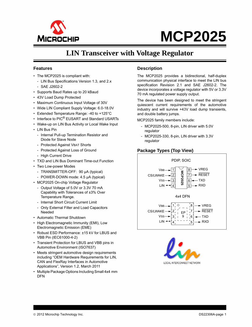
MCP2025LIN Transceiver with Voltage Regulator
Features
• The MCP2025 is compliant with:
- LIN Bus Specifications Version 1.3, and 2.x
- SAE J2602-2
• Supports Baud Rates up to 20 kBaud
• 43V Load Dump Protected
• Maximum Continuous Input Voltage of 30V
• Wide LIN Compliant Supply Voltage: 6.0-18.0V
• Extended Temperature Range: -40 to +125°C
• Interface to PIC® EUSART and Standard USARTs
• Wake-up on LIN Bus Activity or Local Wake Input
• LIN Bus Pin
- Internal Pull-up Termination Resistor and Diode for Slave Node
- Protected Against VBAT Shorts
- Protected Against Loss of Ground
- High Current Drive
• TXD and LIN Bus Dominant Time-out Function
• Two Low-power Modes
- TRANSMITTER-OFF: 90 µA (typical)
- POWER-DOWN mode: 4.5 µA (typical)
• MCP2025 On-chip Voltage Regulator
- Output Voltage of 5.0V or 3.3V 70 mA Capability with Tolerances of ±3% Over Temperature Range.
- Internal Short Circuit Current Limit
- Only External Filter and Load Capacitors Needed
• Automatic Thermal Shutdown
• High Electromagnetic Immunity (EMI), Low Electromagnetic Emission (EME)
• Robust ESD Performance: ±15 kV for LBUS and VBB Pin (IEC61000-4-2)
• Transient Protection for LBUS and VBB pins in Automotive Environment (ISO7637)
• Meets stringent automotive design requirements including “OEM Hardware Requirements for LIN, CAN and FlexRay Interfaces in Automotive Applications”, Version 1.2, March 2011
• Multiple Package Options Including Small 4x4 mm DFN
Description
The MCP2025 provides a bidirectional, half-duplexcommunication physical interface to meet the LIN busspecification Revision 2.1 and SAE J2602-2. Thedevice incorporates a voltage regulator with 5V or 3.3V70 mA regulated power supply output.
The device has been designed to meet the stringentquiescent current requirements of the automotiveindustry and will survive +43V load dump transients,and double battery jumps.
MCP2025 family members include:
- MCP2025-500, 8-pin, LIN driver with 5.0V regulator
- MCP2025-330, 8-pin, LIN driver with 3.3V regulator
Package Types (Top View)
PDIP, SOIC
VSS
CS/LWAKE
LIN
1
2
3
4
8
7
6
5
VBB VREG
RESET
TXD
RXD
4x4 DFN
1
2
3
4
8
7
6
5
EP9VSS
CS/LWAKE
LIN
VBB VREG
RESET
TXD
RXD
MC
P2
02
5
2012 Microchip Technology Inc. DS22306A-page 1
MCP2025
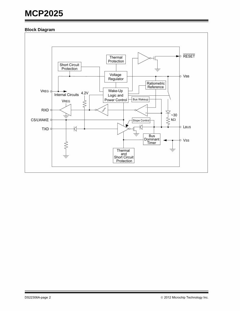
Block Diagram
VoltageRegulator
RatiometricReference
Thermal
Protection
Internal CircuitsVREG
RXD
TXD
VBB
LBUS
VSS
~30CS/LWAKE
Wake-UpLogic and
Power Control
RESET
Short CircuitProtection
ThermalProtection
k
Bus Wakeup
andShort Circuit
Slope Control
VREG
4.2V
BusDominant
Timer
DS22306A-page 2 2012 Microchip Technology Inc.
MCP2025
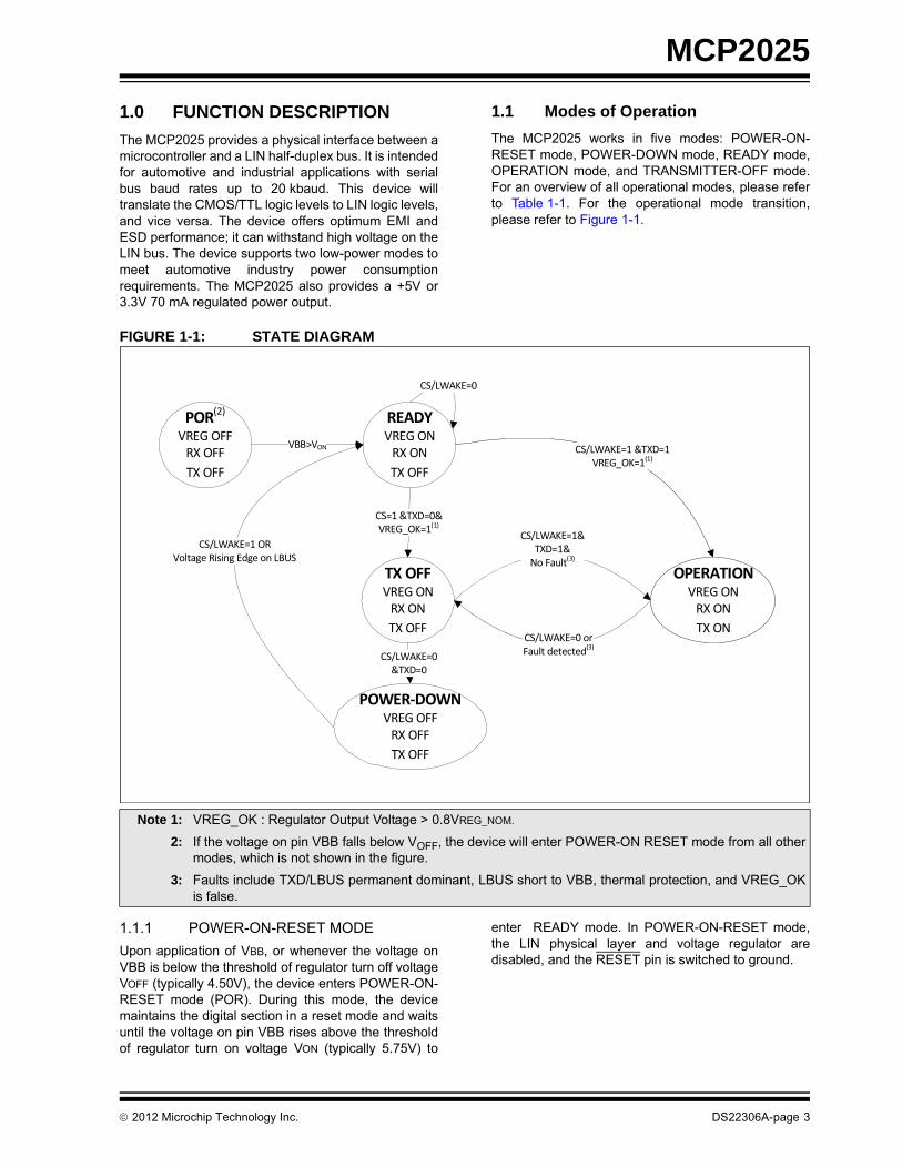
1.0 FUNCTION DESCRIPTION
The MCP2025 provides a physical interface between amicrocontroller and a LIN half-duplex bus. It is intendedfor automotive and industrial applications with serialbus baud rates up to 20 kbaud. This device willtranslate the CMOS/TTL logic levels to LIN logic levels,and vice versa. The device offers optimum EMI andESD performance; it can withstand high voltage on theLIN bus. The device supports two low-power modes tomeet automotive industry power consumptionrequirements. The MCP2025 also provides a +5V or3.3V 70 mA regulated power output.
1.1 Modes of Operation
The MCP2025 works in five modes: POWER-ON-RESET mode, POWER-DOWN mode, READY mode,OPERATION mode, and TRANSMITTER-OFF mode.For an overview of all operational modes, please referto Table 1-1. For the operational mode transition,please refer to Figure 1-1.
FIGURE 1-1: STATE DIAGRAM
1.1.1 POWER-ON-RESET MODE
Upon application of VBB, or whenever the voltage onVBB is below the threshold of regulator turn off voltageVOFF (typically 4.50V), the device enters POWER-ON-RESET mode (POR). During this mode, the devicemaintains the digital section in a reset mode and waitsuntil the voltage on pin VBB rises above the thresholdof regulator turn on voltage VON (typically 5.75V) to
enter READY mode. In POWER-ON-RESET mode,the LIN physical layer and voltage regulator aredisabled, and the RESET pin is switched to ground.
POR(2)
VREG OFFRX OFFTX OFF
READYVREG ON
RX ONTX OFF
TX OFFVREG ON
RX ONTX OFF
POWER-DOWNVREG OFF
RX OFFTX OFF
OPERATIONVREG ON
RX ONTX ON
VBB>VON
CS/LWAKE=0&TXD=0
CS/LWAKE=1 &TXD=1VREG_OK=1(1)
CS/LWAKE=1&TXD=1&
No Fault(3)
CS/LWAKE=0 orFault detected(3)
CS/LWAKE=1 OR Voltage Rising Edge on LBUS
CS/LWAKE=0
CS=1 &TXD=0&VREG_OK=1(1)
Note 1: VREG_OK : Regulator Output Voltage > 0.8VREG_NOM.
2: If the voltage on pin VBB falls below VOFF, the device will enter POWER-ON RESET mode from all othermodes, which is not shown in the figure.
3: Faults include TXD/LBUS permanent dominant, LBUS short to VBB, thermal protection, and VREG_OKis false.
2012 Microchip Technology Inc. DS22306A-page 3
MCP2025
1.1.2 READY MODE
The device enters READY mode from POR mode afterthe voltage on VBB rises above the threshold ofregulator turn on voltage VON or from POWER-DOWNmode when a remote or local wake-up event happens.
Upon entering READY mode, the voltage regulator andreceiver section of the transceiver are powered up. Thetransmitter remains in an off state. The device is readyto receive data but not to transmit. In order to minimizethe power consumption, the regulator operates in areduced power mode. It has a lower GBW product andthus is slower. However, the 70 mA drive capability isunchanged.
The device stays in READY mode until the output of thevoltage regulator has stabilized and CS/LWAKE pin isHIGH (‘1’).
1.1.3 OPERATION MODE
If the CS/LWAKE pin changes to high while VREG is OK(VREG > 0.8*VREG_NOM) and TXD pin is HIGH, the partenters OPERATION mode from either READY orTRANSMITTER-OFF mode.
In this mode, all internal modules are operational. Theinternal pull-up resistor between LBUS and VBB is con-nected only in this mode.
The device goes to TRANSMITTER-OFF mode at thefalling edge on the CS/LWAKE pin or when a fault isdetected.
1.1.4 TRANSMITTER OFF MODE
If VREG is OK (VREG > 0.8*VREG_NOM), the TRANSMIT-TER-OFF mode can be reached by setting CS/LWAKEto HIGH when TXD pin is LOW from READY mode; orby pulling down CS/LWAKE to low from OPERATIONmode.
In TRANSMITTER-OFF mode, the receiver is enabledbut the LBUS transmitter is off. It is a lower power mode.
In order to minimize the power consumption, the regu-lator operates in a reduced power mode. It has a lowerGBW product and thus is slower. However, the 70 mAdrive capability is unchanged.
The transmitter is also turned off whenever the voltageregulator is unstable or recovering from a fault. Thisprevents unwanted disruption on the bus during timesof uncertain operation.
1.1.5 POWER-DOWN MODE
POWER-DOWN mode is entered by pulling down boththe CS/LWAKE pin and TXD to low from TRANSMIT-TER-OFF mode. In POWER-DOWN mode, the trans-ceiver and the voltage regulator are both off. Only theBus Wake-up section and the CS/LWAKE pin wake-upcircuits are in operation. This is the lowest power mode.
If any bus activity (e.g. a BREAK character) occurs orCS/LWAKE is set to HIGH during POWER-DOWNmode, the device will immediately enter READY modeand enable the voltage regulator. Then, once the regu-lator output has stabilized (approximately 0.3 ms to1.2 ms) it can go to either the OPERATION mode orTRANSMITTER-OFF mode. Refer to Section 1.1.6“Remote Wake-up” for more details.
1.1.6 REMOTE WAKE-UP
The remote wake-up sub module observes the LBUS inorder to detect bus activity. In POWER-DOWN mode,the normal LIN recessive/dominant threshold isdisabled, and the LIN bus Wake-Up Voltage ThresholdVWK(LBUS) is used to detect bus activities. Bus activityis detected when the voltage on the LBUS falls belowthe LIN bus Wake-Up Voltage Threshold VWK(LBUS)(approximately 3.4V) for at least tBDB (a typical durationof 80 µs ) followed by a rising edge. Such a conditioncauses the device to leave POWER-DOWN mode.
Note: The TXD pin needs to be set high beforesetting the CS/LWAKE pin to low in orderto jump and stay in TRANSMITTER-OFFmode. If the TXD pin is set or maintainedlow before setting the CS/LWAKE pin tolow, the part will transit to TRANSMITTER-OFF mode and then jump to POWER-DOWN mode after a deglitch delay ofabout 20 µs.
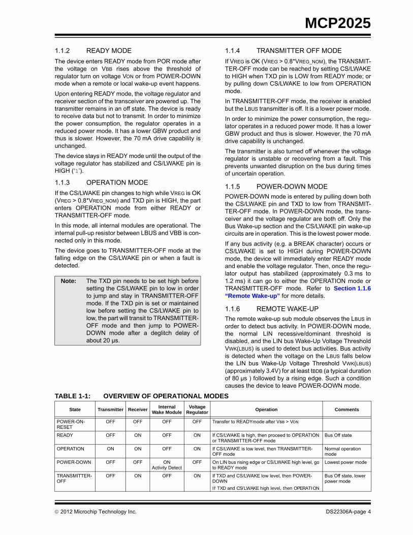
TABLE 1-1: OVERVIEW OF OPERATIONAL MODES
State Transmitter ReceiverInternal
Wake ModuleVoltage
RegulatorOperation Comments
POWER-ON-RESET
OFF OFF OFF OFF Transfer to READYmode after VBB > VON
READY OFF ON OFF ON If CS/LWAKE is high, then proceed to OPERATION or TRANSMITTER-OFF mode
Bus Off state
OPERATION ON ON OFF ON If CS/LWAKE is low level, then TRANSMITTER-OFF mode
Normal operation mode
POWER-DOWN OFF OFF ONActivity Detect
OFF On LIN bus rising edge or CS/LWAKE high level, go to READY mode
Lowest power mode
TRANSMITTER-OFF
OFF ON OFF ON If TXD and CS/LWAKE low level, then POWER-DOWN
If TXD and CS/LWAKE high level, then OPERATION
Bus Off state, lower power mode
2012 Microchip Technology Inc. DS22306A-page 4
MCP2025
1.2 Pin Descriptions
Please refer to Table 1-2 for the pinout overview.
1.2.1 VBB
Battery Positive Supply Voltage pin. An external diodeis connected in series to prevent the device from beingreversely powered (refer to Figure 1-9).
1.2.2 VREG
Positive Supply Voltage Regulator Output pin. An on-chip Low Dropout Regulator (LDO) gives +5.0 or +3.3V70 mA regulated voltage on this pin.
1.2.3 VSS
Ground pin.
1.2.4 TXD
Transmit data input pin (TTL level, HV compliant,adaptive pull-up). The transmitter reads the datastream on the TXD pin and sends it to the LIN bus. TheLBUS pin is low (dominant) when TXD is low, and high(recessive) when TXD is high.
The Transmit Data Input pin has an internal adaptivepull-up to an internally-generated 4.2V(approximately). When TXD is ‘0’, a weak pull-up(~900 kΩ) is used to reduce current. When TXD is ‘1’a stronger pull-up (~300 kΩ) is used to maintain thelogic level. A series reverse-blocking diode allowsapplying TXD input voltages greater than the internallygenerated 4.2V and renders the TXD pin HV compliantup to 30V (see Block Diagram).
1.2.5 RXD
Receive Data Output pin. The RXD pin is a standardCMOS output pin and it follows the state of the LBUSpin.
1.2.6 LBUS
LIN Bus pin. LBUS is a bidirectional LIN bus Interfacepin and is controlled by the signal TXD. It has an opencollector output with a current limitation. To reduce
ElectroMagnetic Emission, the slopes during signalchanges are controlled, and the LBUS pin has corner-rounding control for both falling and rising edges.
The internal LIN receiver observes the activities on theLIN bus, and generates the output signal RXD thatfollows the state of the LBUS. A first degree 160 KHz,low-pass input filter optimizes ElectroMagneticimmunity.
1.2.7 CS/LWAKE
Chip Select and Local Wake-up Input pin (TTL level,high voltage tolerant). This pin controls the device statetransition. Refer to Figure 1-1.
An internal pull-down resistor will keep the CS/LWAKEpin low to ensure that no disruptive data will be presenton the bus while the microcontroller is executing aPOWER-ON RESET and I/O initialization sequence.When CS/LWAKE is ‘1’, a weak pull-down (~600 KΩ) isused to reduce current. When CS/LWAKE is ‘0’ astronger pull-down (~300 KΩ) is used to maintain thelogic level.
This pin may also be used as a local wake-up input(See Figure 1-9). The microcontroller will set the I/O pinto control the CS/LWAKE. An external switch, or othersource, can then wake-up both the transceiver and themicrocontroller.
1.2.8 RESET
RESET OUTPUT pin. This is an open drain output pin.It indicates the internal voltage has reached a valid,stable level. As long as the internal voltage is valid(above 0.8VREG), this pin will present high impedance;otherwise the RESET pin switches to ground.
TABLE 1-2: PINOUT OVERVIEW
Note: CS/LWAKE should NOT be tied directly to pin VREG as this could force the MCP2025 into OPERATION mode before the microcontroller is initialized.
PIN Name PIN Number PIN Type Function
VREG 8 Output Voltage regulator output
VSS 3 Power Ground
VBB 1 Power Battery
TXD 6 Input, HV-tolerant Transmit data input
RXD 5 Output Receive data output
LBUS 4 I/O, HV LIN Bus
CS/LWAKE 2 TTL Input, HV-tolerant Chip Select and Local Wake-up input
RESET 7 Open Drain Output, HV-tolerant
Reset output
2012 Microchip Technology Inc. DS22306A-page 5
MCP2025
1.3 Fail-Safe Features
1.3.1 GENERAL FAIL-SAFE FEATURES
• An internal pull-down resistor on the CS/LWAKE pin disables the transmitter if the pin is floating.
• An internal pull-up resistor on the TXD pin places TXD in HIGH, thus the LBUS is recessive if the TXD pin is floating.
• High-impedance and low leakage current on LBUS during loss of power or ground.
• The current limit on LBUS protects the transceiver from being damaged if the pin is shorted to VBB.
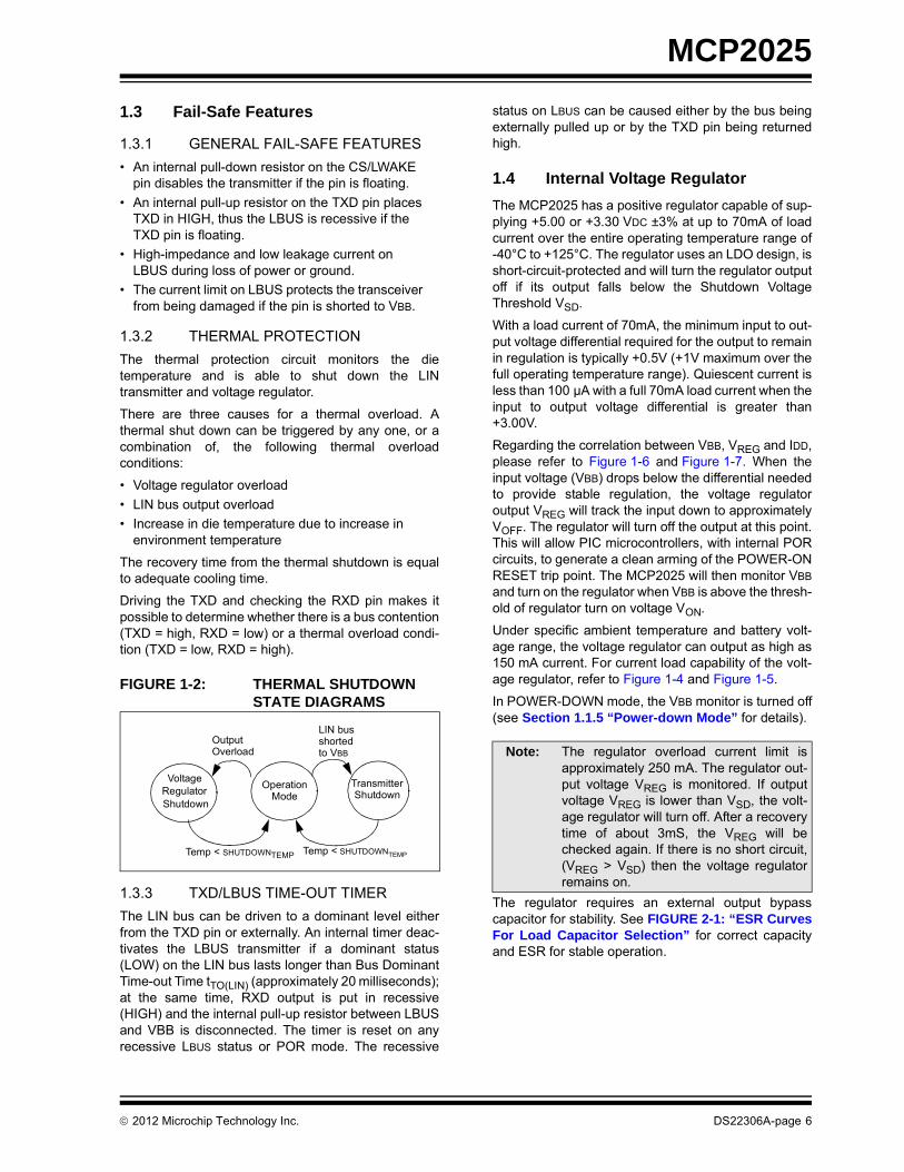
1.3.2 THERMAL PROTECTION
The thermal protection circuit monitors the dietemperature and is able to shut down the LINtransmitter and voltage regulator.
There are three causes for a thermal overload. Athermal shut down can be triggered by any one, or acombination of, the following thermal overloadconditions:
• Voltage regulator overload
• LIN bus output overload
• Increase in die temperature due to increase in environment temperature
The recovery time from the thermal shutdown is equalto adequate cooling time.
Driving the TXD and checking the RXD pin makes itpossible to determine whether there is a bus contention(TXD = high, RXD = low) or a thermal overload condi-tion (TXD = low, RXD = high).
FIGURE 1-2: THERMAL SHUTDOWN STATE DIAGRAMS
1.3.3 TXD/LBUS TIME-OUT TIMER
The LIN bus can be driven to a dominant level eitherfrom the TXD pin or externally. An internal timer deac-tivates the LBUS transmitter if a dominant status(LOW) on the LIN bus lasts longer than Bus DominantTime-out Time tTO(LIN) (approximately 20 milliseconds);at the same time, RXD output is put in recessive(HIGH) and the internal pull-up resistor between LBUSand VBB is disconnected. The timer is reset on anyrecessive LBUS status or POR mode. The recessive
status on LBUS can be caused either by the bus beingexternally pulled up or by the TXD pin being returnedhigh.
1.4 Internal Voltage Regulator
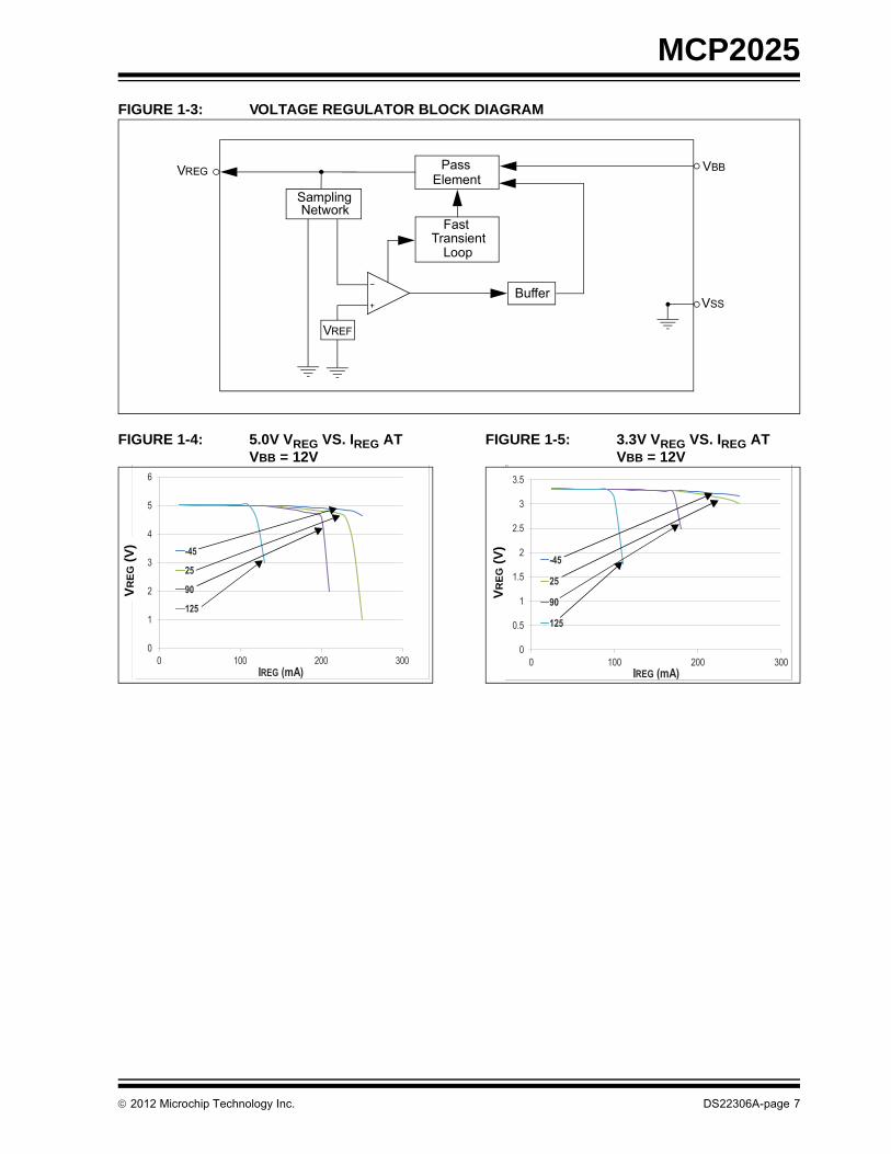
The MCP2025 has a positive regulator capable of sup-plying +5.00 or +3.30 VDC ±3% at up to 70mA of loadcurrent over the entire operating temperature range of-40°C to +125°C. The regulator uses an LDO design, isshort-circuit-protected and will turn the regulator outputoff if its output falls below the Shutdown VoltageThreshold VSD.
With a load current of 70mA, the minimum input to out-put voltage differential required for the output to remainin regulation is typically +0.5V (+1V maximum over thefull operating temperature range). Quiescent current isless than 100 µA with a full 70mA load current when theinput to output voltage differential is greater than+3.00V.
Regarding the correlation between VBB, VREG and IDD,please refer to Figure 1-6 and Figure 1-7. When theinput voltage (VBB) drops below the differential neededto provide stable regulation, the voltage regulatoroutput VREG will track the input down to approximatelyVOFF. The regulator will turn off the output at this point.This will allow PIC microcontrollers, with internal PORcircuits, to generate a clean arming of the POWER-ONRESET trip point. The MCP2025 will then monitor VBB
and turn on the regulator when VBB is above the thresh-old of regulator turn on voltage VON.
Under specific ambient temperature and battery volt-age range, the voltage regulator can output as high as150 mA current. For current load capability of the volt-age regulator, refer to Figure 1-4 and Figure 1-5.
In POWER-DOWN mode, the VBB monitor is turned off(see Section 1.1.5 “Power-down Mode” for details).
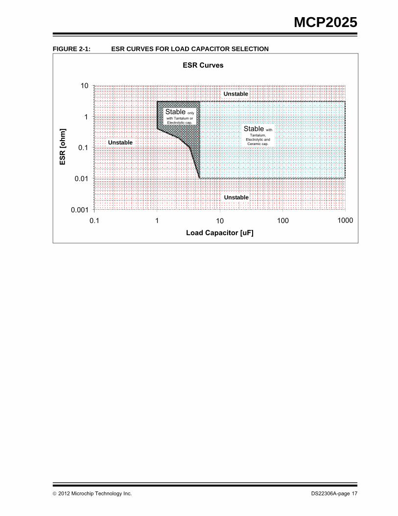
The regulator requires an external output bypasscapacitor for stability. See FIGURE 2-1: “ESR CurvesFor Load Capacitor Selection” for correct capacityand ESR for stable operation.
OperationMode
TransmitterShutdown
LIN bus
Voltage
ShutdownRegulator
Output
Temp < SHUTDOWNTEMP
shortedto VBBOverload
Temp < SHUTDOWNTEMP
Note: The regulator overload current limit isapproximately 250 mA. The regulator out-put voltage VREG is monitored. If outputvoltage VREG is lower than VSD, the volt-age regulator will turn off. After a recoverytime of about 3mS, the VREG will bechecked again. If there is no short circuit,(VREG > VSD) then the voltage regulatorremains on.
2012 Microchip Technology Inc. DS22306A-page 6
MCP2025
FIGURE 1-3: VOLTAGE REGULATOR BLOCK DIAGRAM
FIGURE 1-4: 5.0V VREG VS. IREG AT VBB = 12V
FIGURE 1-5: 3.3V VREG VS. IREG AT VBB = 12V
PassElement
Sampling Network
Buffer
VREG VBB
VSS
FastTransient
Loop
VREF
0
1
2
3
4
5
6
0 100 200 300IREG (mA)
-45
25
90
125
VR
EG
(V
)
0
0.5
1
1.5
2
2.5
3
3.5
0 100 200 300IREG (mA)
-45
25
90
125
0
0.5
1
1.5
2
2.5
3
3.5
0 100 200 300IREG (mA)
-45
25
90
125
0
0.5
1
1.5
2
2.5
3
3.5
0 100 200 300IREG (mA)
-45
25
90
125
0
0.5
1
1.5
2
2.5
3
3.5
0 100 200 300IREG (mA)
-45
25
90
125
0
0.5
1
1.5
2
2.5
3
3.5
0 100 200 300IREG (mA)
-45
25
90
125
0
0.5
1
1.5
2
2.5
3
3.5
0 100 200 300IREG (mA)
-45
25
90
125
0
0.5
1
1.5
2
2.5
3
3.5
0 100 200 300IREG (mA)
-45
25
90
125
0
0.5
1
1.5
2
2.5
3
3.5
0 100 200 300IREG (mA)
-45
25
90
125
0
0.5
1
1.5
2
2.5
3
3.5
0 100 200 300IREG (mA)
-45
25
90
125
0
0.5
1
1.5
2
2.5
3
3.5
0 100 200 300IREG (mA)
-45
25
90
125
0
0.5
1
1.5
2
2.5
3
3.5
0 100 200 300IREG (mA)
-45
25
90
125
0
0.5
1
1.5
2
2.5
3
3.5
0 100 200 300IREG (mA)
-45
25
90
125
0
0.5
1
1.5
2
2.5
3
3.5
0 100 200 300IREG (mA)
-45
25
90
125
0
0.5
1
1.5
2
2.5
3
3.5
0 100 200 300IREG (mA)
-45
25
90
125
0
0.5
1
1.5
2
2.5
3
3.5
0 100 200 300IREG (mA)
-45
25
90
125
0
0.5
1
1.5
2
2.5
3
3.5
0 100 200 300IREG (mA)
-45
25
90
125
0
0.5
1
1.5
2
2.5
3
3.5
0 100 200 300IREG (mA)
-45
25
90
125
0
0.5
1
1.5
2
2.5
3
3.5
0 100 200 300IREG (mA)
-45
25
90
125
0
0.5
1
1.5
2
2.5
3
3.5
0 100 200 300IREG (mA)
-45
25
90
125
0
0.5
1
1.5
2
2.5
3
3.5
0 100 200 300IREG (mA)
-45
25
90
125
0
0.5
1
1.5
2
2.5
3
3.5
0 100 200 300IREG (mA)
-45
25
90
125
0
0.5
1
1.5
2
2.5
3
3.5
0 100 200 300IREG (mA)
-45
25
90
125
0
0.5
1
1.5
2
2.5
3
3.5
0 100 200 300IREG (mA)
-45
25
90
125
0
0.5
1
1.5
2
2.5
3
3.5
0 100 200 300IREG (mA)
-45
25
90
125
0
0.5
1
1.5
2
2.5
3
3.5
0 100 200 300IREG (mA)
-45
25
90
125
0
0.5
1
1.5
2
2.5
3
3.5
0 100 200 300IREG (mA)
-45
25
90
125
0
0.5
1
1.5
2
2.5
3
3.5
0 100 200 300IREG (mA)
-45
25
90
125
0
0.5
1
1.5
2
2.5
3
3.5
0 100 200 300IREG (mA)
-45
25
90
125
0
0.5
1
1.5
2
2.5
3
3.5
0 100 200 300IREG (mA)
-45
25
90
125
0
0.5
1
1.5
2
2.5
3
3.5
0 100 200 300IREG (mA)
-45
25
90
125
0
0.5
1
1.5
2
2.5
3
3.5
0 100 200 300IREG (mA)
-45
25
90
125
0
0.5
1
1.5
2
2.5
3
3.5
0 100 200 300IREG (mA)
-45
25
90
125
0
0.5
1
1.5
2
2.5
3
3.5
0 100 200 300IREG (mA)
-45
25
90
125
0
0.5
1
1.5
2
2.5
3
3.5
0 100 200 300IREG (mA)
-45
25
90
125
0
0.5
1
1.5
2
2.5
3
3.5
0 100 200 300IREG (mA)
-45
25
90
125
0
0.5
1
1.5
2
2.5
3
3.5
0 100 200 300IREG (mA)
-45
25
90
125
0
0.5
1
1.5
2
2.5
3
3.5
0 100 200 300IREG (mA)
-45
25
90
125
0
0.5
1
1.5
2
2.5
3
3.5
0 100 200 300IREG (mA)
-45
25
90
125
0
0.5
1
1.5
2
2.5
3
3.5
0 100 200 300IREG (mA)
-45
25
90
125
0
0.5
1
1.5
2
2.5
3
3.5
0 100 200 300IREG (mA)
-45
25
90
125
0
0.5
1
1.5
2
2.5
3
3.5
0 100 200 300IREG (mA)
-45
25
90
125
0
0.5
1
1.5
2
2.5
3
3.5
0 100 200 300IREG (mA)
-45
25
90
125
0
0.5
1
1.5
2
2.5
3
3.5
0 100 200 300IREG (mA)
-45
25
90
125
0
0.5
1
1.5
2
2.5
3
3.5
0 100 200 300IREG (mA)
-45
25
90
125
0
0.5
1
1.5
2
2.5
3
3.5
0 100 200 300IREG (mA)
-45
25
90
125
0
0.5
1
1.5
2
2.5
3
3.5
0 100 200 30IREG (mA)
-45
25
90
125
0
0.5
1
1.5
2
2.5
3
3.5
0 100 200 30IREG (mA)
-45
25
90
125
0
0.5
1
1.5
2
2.5
3
3.5
0 100 200 30IREG (mA)
-45
25
90
125
0
0.5
1
1.5
2
2.5
3
3.5
0 100 200 30IREG (mA)
-45
25
90
125
0
0.5
1
1.5
2
2.5
3
3.5
0 100 200 30IREG (mA)
-45
25
90
125
0
0.5
1
1.5
2
2.5
3
3.5
0 100 200 30IREG (mA)
-45
25
90
125
0
0.5
1
1.5
2
2.5
3
3.5
0 100 200 300IREG (mA)
-45
25
90
125
0
0.5
1
1.5
2
2.5
3
3.5
0 100 200 300IREG (mA)
-45
25
90
125
0
0.5
1
1.5
2
2.5
3
3.5
0 100 200 300IREG (mA)
-45
25
90
125
0
0.5
1
1.5
2
2.5
3
3.5
0 100 200 300IREG (mA)
-45
25
90
125
0
0.5
1
1.5
2
2.5
3
3.5
0 100 200 300IREG (mA)
-45
25
90
125
0
0.5
1
1.5
2
2.5
3
3.5
0 100 200 300IREG (mA)
-45
25
90
125
0
0.5
1
1.5
2
2.5
3
3.5
0 100 200 300IREG (mA)
-45
25
90
125
0
0.5
1
1.5
2
2.5
3
3.5
0 100 200 300IREG (mA)
-45
25
90
125
0
0.5
1
1.5
2
2.5
3
3.5
0 100 200 300IREG (mA)
-45
25
90
125
0
0.5
1
1.5
2
2.5
3
3.5
0 100 200 300IREG (mA)
-45
25
90
125
0
0.5
1
1.5
2
2.5
3
3.5
0 100 200 300IREG (mA)
-45
25
90
125
0
0.5
1
1.5
2
2.5
3
3.5
0 100 200 300IREG (mA)
-45
25
90
125
0
0.5
1
1.5
2
2.5
3
3.5
0 100 200 300IREG (mA)
-45
25
90
125
0
0.5
1
1.5
2
2.5
3
3.5
0 100 200 300IREG (mA)
-45
25
90
125
0
0.5
1
1.5
2
2.5
3
3.5
0 100 200 300IREG (mA)
-45
25
90
125
0
0.5
1
1.5
2
2.5
3
3.5
0 100 200 300IREG (mA)
-45
25
90
125
0
0.5
1
1.5
2
2.5
3
3.5
0 100 200 300IREG (mA)
-45
25
90
125
0
0.5
1
1.5
2
2.5
3
3.5
0 100 200 300IREG (mA)
-45
25
90
125
0
0.5
1
1.5
2
2.5
3
3.5
0 100 200 300IREG (mA)
-45
25
90
125
0
0.5
1
1.5
2
2.5
3
3.5
0 100 200 300IREG (mA)
-45
25
90
125
0
0.5
1
1.5
2
2.5
3
3.5
0 100 200 300IREG (mA)
-45
25
90
125
0
0.5
1
1.5
2
2.5
3
3.5
0 100 200 300IREG (mA)
-45
25
90
125
VR
EG
(V
)
2012 Microchip Technology Inc. DS22306A-page 7
MCP2025
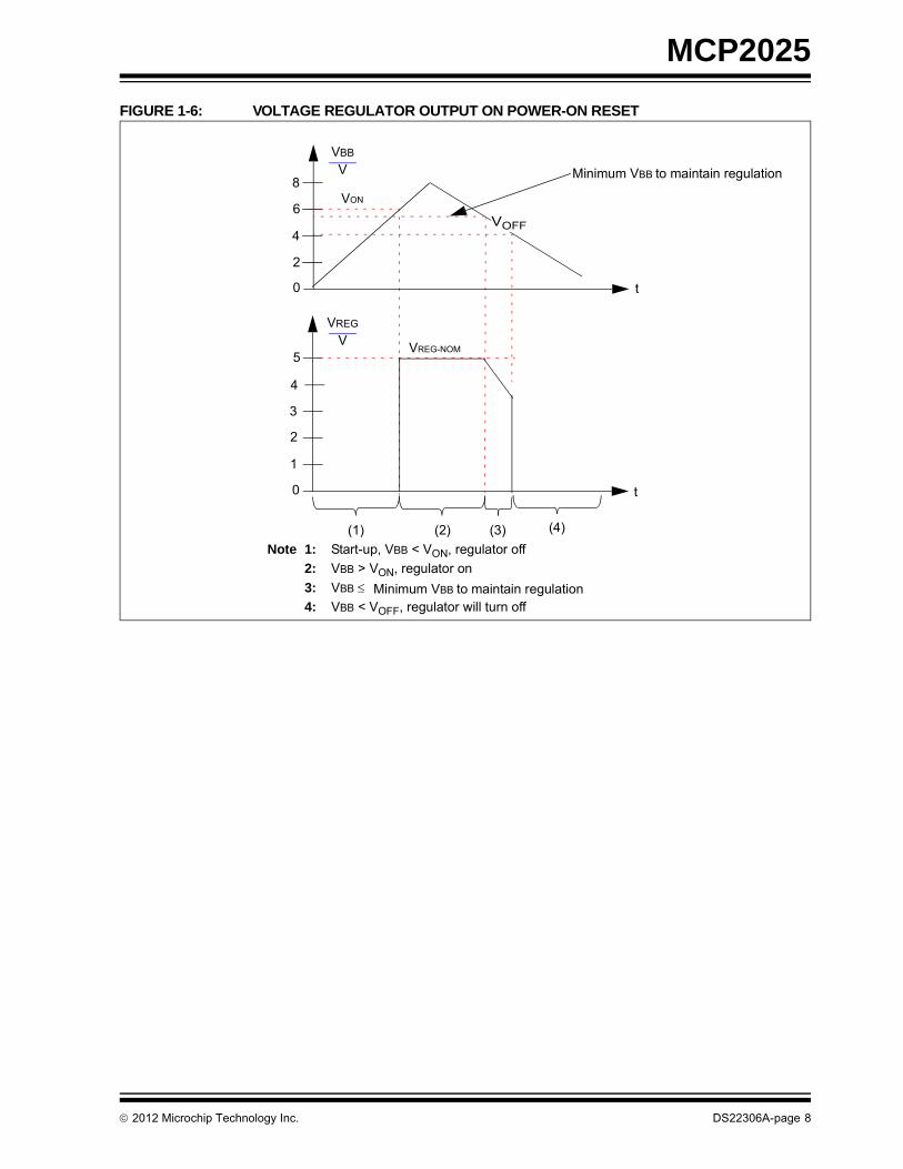
FIGURE 1-6: VOLTAGE REGULATOR OUTPUT ON POWER-ON RESET
Note 1: Start-up, VBB < VON, regulator off
2: VBB > VON, regulator on .
3: VBB 4: VBB < VOFF, regulator will turn off
5
3
2
0
(1) (2) (3)
t
0 t
6
2
8
4
VBB
V
VREG
V
1
4
VON
Minimum VBB to maintain regulation
VREG-NOM
Minimum VBB to maintain regulation
(4)
VOFF
2012 Microchip Technology Inc. DS22306A-page 8
MCP2025
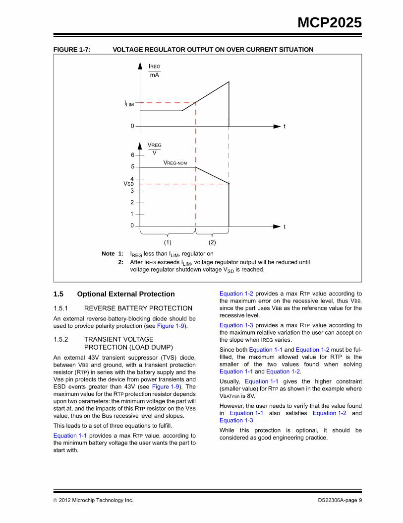
FIGURE 1-7: VOLTAGE REGULATOR OUTPUT ON OVER CURRENT SITUATION
1.5 Optional External Protection
1.5.1 REVERSE BATTERY PROTECTION
An external reverse-battery-blocking diode should beused to provide polarity protection (see Figure 1-9).
1.5.2 TRANSIENT VOLTAGE PROTECTION (LOAD DUMP)
An external 43V transient suppressor (TVS) diode,between VBB and ground, with a transient protectionresistor (RTP) in series with the battery supply and theVBB pin protects the device from power transients andESD events greater than 43V (see Figure 1-9). Themaximum value for the RTP protection resistor dependsupon two parameters: the minimum voltage the part willstart at, and the impacts of this RTP resistor on the VBB
value, thus on the Bus recessive level and slopes.
This leads to a set of three equations to fulfill.
Equation 1-1 provides a max RTP value, according tothe minimum battery voltage the user wants the part tostart with.
Equation 1-2 provides a max RTP value according tothe maximum error on the recessive level, thus VBB,
since the part uses VBB as the reference value for therecessive level.
Equation 1-3 provides a max RTP value according tothe maximum relative variation the user can accept onthe slope when IREG varies.
Since both Equation 1-1 and Equation 1-2 must be ful-filled, the maximum allowed value for RTP is thesmaller of the two values found when solvingEquation 1-1 and Equation 1-2.
Usually, Equation 1-1 gives the higher constraint(smaller value) for RTP as shown in the example whereVBATmin is 8V.
However, the user needs to verify that the value foundin Equation 1-1 also satisfies Equation 1-2 andEquation 1-3.
While this protection is optional, it should beconsidered as good engineering practice.
Note 1: IREG less than ILIM, regulator on
2: After IREG exceeds ILIM, voltage regulator output will be reduced until voltage regulator shutdown voltage VSD is reached.
VSD
0
(1) (2)
t
0 t
ILIM
IREG
mA
VREG
V
VREG-NOM
1
2
3
4
5
6
2012 Microchip Technology Inc. DS22306A-page 9
MCP2025
EQUATION 1-1:
Assume that VBATmin = 8V. Equation 1-1 gives 10.
EQUATION 1-2:
Assume that ∆VRECCESSIVE = 1V and IREGMAX=50 mA.Equation 1-2 gives 20.
EQUATION 1-3:
Assume that ∆Slope =15%, VBATmin=8V andIREGMAX = 50 mA. Equation 1-3 gives 20.
1.5.3 CBAT CAP
Selecting CBAT = 10* CREG is recommended, howeverthis leads to a high value cap. Lower values for CBAT
cap can be used, but certain rules must be followed. Inany case, the voltage at the VBB pin should remainabove VOFF when the device is turned on.
The current peak at start-up (due to the fast charge ofthe CREG and CBAT capacitor) may induce a significantdrop on the VBB pin. This drop is proportional to theimpedance of the VBAT connection (see Figure 1-9).
Let’s assume that the VBAT connection is mainly induc-tive and resistive, and that the customer knows theresistive and inductive values of the connection.
The following formula gives an indication of theminimum value the customer should use for CBAT:
EQUATION 1-4:
Equation 1-4 allows lower CBAT/CREG values than the10* ratio we recommend.
Assumee that we have a good quality connection withRTOT = 0.1 and L = 0.1 mH.
Solving the equation results in CBAT/CREG = 1.
If RTOT is increased to 1, the result becomes CBAT/CREG = 1.4
But if the connection is highly resistive or highly induc-tive (poor connection), the CBAT/CREG ratio greatlyincreases.
For a highly inductive connection: RTOT = 0.1 and L =1 mH; the CBAT/CREG ratio increases to 7.
For a highly resistive connection: RTOT = 10 andL = 0.1 mH: again, the CBAT/CREG ratio increases to 7.
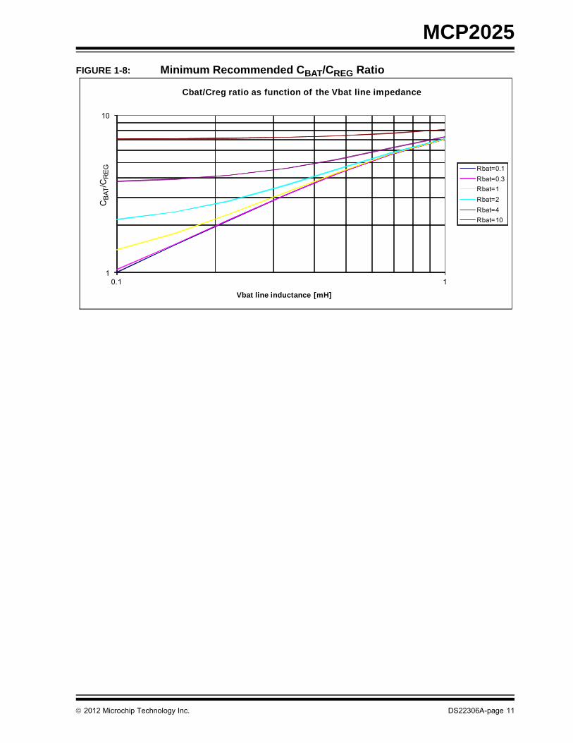
Figure 1-8 shows the minimum recommended CBAT/CREG ratio as a function of the impedance of the VBAT
connection.
250 mA is the peak current at power-on when VBB = 5.5V
RTP <= ∆VRECCESSIVE / IREGMAX.∆VRECCESSIVE is the maximum variation tolerated on
the recessive level
∆Slope is the maximum variation tolerated on the slope level and Iregmax is the maximum current the regulator will provide to the load. VBATmin>VOFF + 1.0V,
RTP
VBATmin 5.5V–250mA
-------------------------------------
5.5V VOFF 1.0V+=
RTP
Slope VBATmin 1V– Iregmax
--------------------------------------------------------------
where L is in mH and RTOT in . RTOT = RLINE + RTP
CBAT
CREG-------------
100L2
Rtot2+
1 L2 Rtot
2
100---------+ +
-------------------------------=
2012 Microchip Technology Inc. DS22306A-page 10
MCP2025
FIGURE 1-8: Minimum Recommended CBAT/CREG Ratio
CB
AT/C
RE
G
1
10
0.1 1
Vbat line inductance [mH]
Cbat/Creg ratio as function of the Vbat line impedance
Rbat=0.1
Rbat=0.3
Rbat=1
Rbat=2
Rbat=4
Rbat=10
CB
AT/C
RE
G
2012 Microchip Technology Inc. DS22306A-page 11
MCP2025
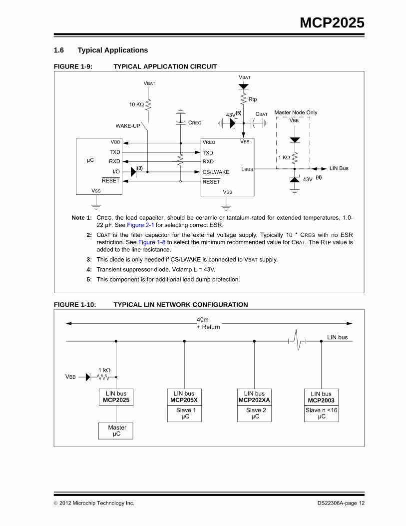
1.6 Typical Applications
FIGURE 1-9: TYPICAL APPLICATION CIRCUIT
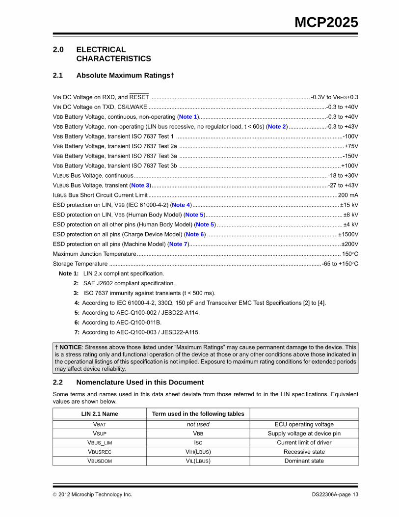
FIGURE 1-10: TYPICAL LIN NETWORK CONFIGURATION
LIN Bus
43V (4)
VBB
LBUS
VREG
TXD
RXD
VSS
VDD
TXD
RXDµC
VBAT
CBAT
CREG
CS/LWAKEI/O
43V(5)
1 K
VBB
Master Node Only
VBAT
10 K
WAKE-UP
Note 1: CREG, the load capacitor, should be ceramic or tantalum-rated for extended temperatures, 1.0-22 µF. See Figure 2-1 for selecting correct ESR.
2: CBAT is the filter capacitor for the external voltage supply. Typically 10 * CREG with no ESRrestriction. See Figure 1-8 to select the minimum recommended value for CBAT. The RTP value isadded to the line resistance.
3: This diode is only needed if CS/LWAKE is connected to VBAT supply.
4: Transient suppressor diode. Vclamp L = 43V.
5: This component is for additional load dump protection.
(3)
Rtp
RESETRESET
VSS
LIN busMCP2025
MasterµC
1 kVBB
Slave 1µC
Slave 2µC
Slave n <16µC
40m+ Return
LIN bus
LIN busMCP205X
LIN busMCP202XA
LIN busMCP2003
2012 Microchip Technology Inc. DS22306A-page 12
MCP2025
2.0 ELECTRICAL CHARACTERISTICS
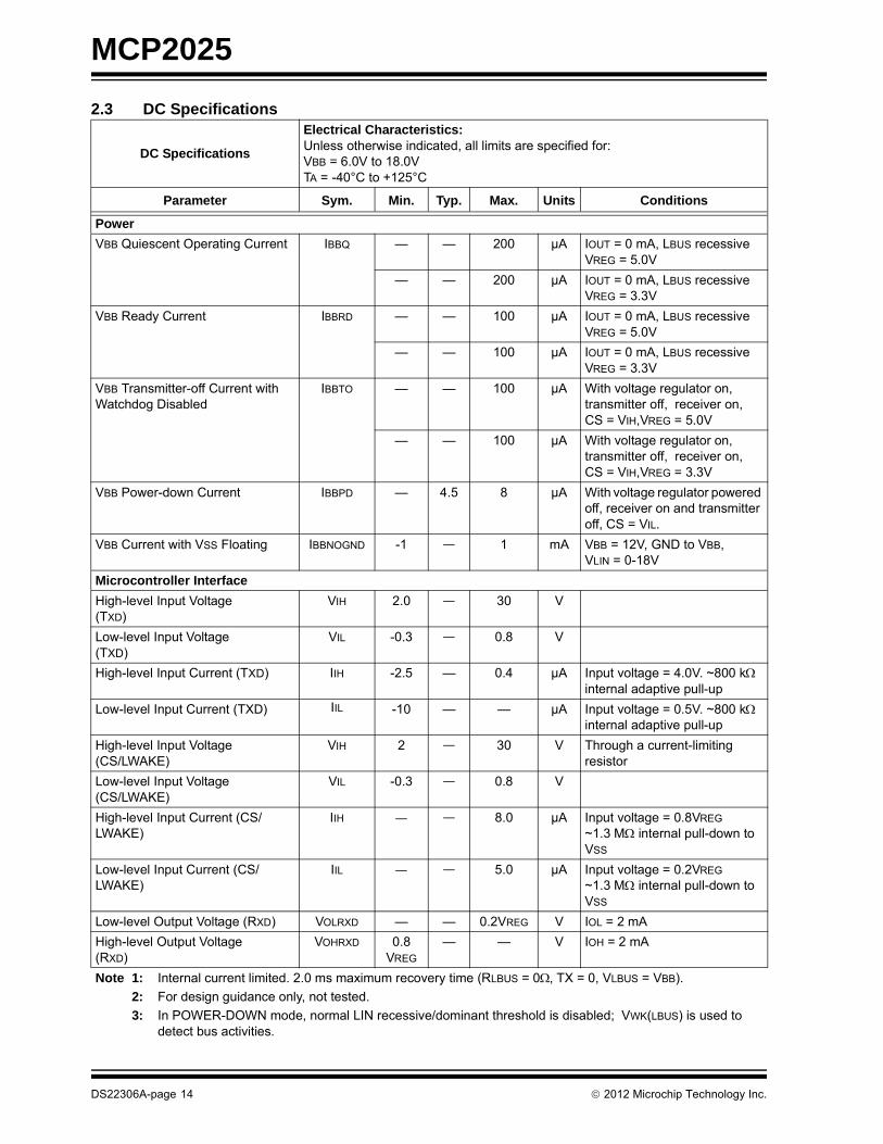
2.1 Absolute Maximum Ratings†
VIN DC Voltage on RXD, and RESET ................................................................................................. -0.3V to VREG+0.3
VIN DC Voltage on TXD, CS/LWAKE .............................................................................................................-0.3 to +40V
VBB Battery Voltage, continuous, non-operating (Note 1)..............................................................................-0.3 to +40V
VBB Battery Voltage, non-operating (LIN bus recessive, no regulator load, t < 60s) (Note 2) .......................-0.3 to +43V
VBB Battery Voltage, transient ISO 7637 Test 1 ......................................................................................................-100V
VBB Battery Voltage, transient ISO 7637 Test 2a .....................................................................................................+75V
VBB Battery Voltage, transient ISO 7637 Test 3a ....................................................................................................-150V
VBB Battery Voltage, transient ISO 7637 Test 3b ...................................................................................................+100V
VLBUS Bus Voltage, continuous.......................................................................................................................-18 to +30V
VLBUS Bus Voltage, transient (Note 3) ............................................................................................................-27 to +43V
ILBUS Bus Short Circuit Current Limit ....................................................................................................................200 mA
ESD protection on LIN, VBB (IEC 61000-4-2) (Note 4) .......................................................................................... ±15 kV
ESD protection on LIN, VBB (Human Body Model) (Note 5).................................................................................... ±8 kV
ESD protection on all other pins (Human Body Model) (Note 5) ............................................................................. ±4 kV
ESD protection on all pins (Charge Device Model) (Note 6) ................................................................................±1500V
ESD protection on all pins (Machine Model) (Note 7).............................................................................................±200V
Maximum Junction Temperature............................................................................................................................. 150C
Storage Temperature .................................................................................................................................. -65 to +150C
Note 1: LIN 2.x compliant specification.
2: SAE J2602 compliant specification.
3: ISO 7637 immunity against transients (t < 500 ms).
4: According to IEC 61000-4-2, 330Ω, 150 pF and Transceiver EMC Test Specifications [2] to [4].
5: According to AEC-Q100-002 / JESD22-A114.
6: According to AEC-Q100-011B.
7: According to AEC-Q100-003 / JESD22-A115.
2.2 Nomenclature Used in this Document
Some terms and names used in this data sheet deviate from those referred to in the LIN specifications. Equivalentvalues are shown below.
† NOTICE: Stresses above those listed under “Maximum Ratings” may cause permanent damage to the device. Thisis a stress rating only and functional operation of the device at those or any other conditions above those indicated inthe operational listings of this specification is not implied. Exposure to maximum rating conditions for extended periodsmay affect device reliability.
LIN 2.1 Name Term used in the following tables
VBAT not used ECU operating voltage
VSUP VBB Supply voltage at device pin
VBUS_LIM ISC Current limit of driver
VBUSREC VIH(LBUS) Recessive state
VBUSDOM VIL(LBUS) Dominant state
2012 Microchip Technology Inc. DS22306A-page 13
MCP2025
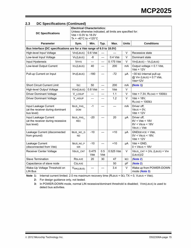
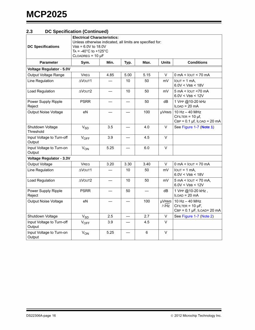
2.3 DC Specifications
DC Specifications
Electrical Characteristics: Unless otherwise indicated, all limits are specified for:VBB = 6.0V to 18.0V TA = -40°C to +125°C
Parameter Sym. Min. Typ. Max. Units Conditions
Power
VBB Quiescent Operating Current IBBQ — — 200 µA IOUT = 0 mA, LBUS recessiveVREG = 5.0V
— — 200 µA IOUT = 0 mA, LBUS recessiveVREG = 3.3V
VBB Ready Current IBBRD — — 100 µA IOUT = 0 mA, LBUS recessiveVREG = 5.0V
— — 100 µA IOUT = 0 mA, LBUS recessiveVREG = 3.3V
VBB Transmitter-off Current with Watchdog Disabled
IBBTO — — 100 µA With voltage regulator on, transmitter off, receiver on, CS = VIH,VREG = 5.0V
— — 100 µA With voltage regulator on, transmitter off, receiver on, CS = VIH,VREG = 3.3V
VBB Power-down Current IBBPD — 4.5 8 µA With voltage regulator powered off, receiver on and transmitter off, CS = VIL.
VBB Current with VSS Floating IBBNOGND -1 — 1 mA VBB = 12V, GND to VBB, VLIN = 0-18V
Microcontroller Interface
High-level Input Voltage(TXD)
VIH 2.0 — 30 V
Low-level Input Voltage(TXD)
VIL -0.3 — 0.8 V
High-level Input Current (TXD) IIH -2.5 — 0.4 µA Input voltage = 4.0V. ~800 k internal adaptive pull-up
Low-level Input Current (TXD) IIL -10 — — µA Input voltage = 0.5V. ~800 k internal adaptive pull-up
High-level Input Voltage(CS/LWAKE)
VIH 2 — 30 V Through a current-limiting resistor
Low-level Input Voltage(CS/LWAKE)
VIL -0.3 — 0.8 V
High-level Input Current (CS/LWAKE)
IIH — — 8.0 µA Input voltage = 0.8VREG
~1.3 M internal pull-down to VSS
Low-level Input Current (CS/LWAKE)
IIL — — 5.0 µA Input voltage = 0.2VREG
~1.3 M internal pull-down to VSS
Low-level Output Voltage (RXD) VOLRXD — — 0.2VREG V IOL = 2 mA
High-level Output Voltage(RXD)
VOHRXD 0.8VREG
— — V IOH = 2 mA
Note 1: Internal current limited. 2.0 ms maximum recovery time (RLBUS = 0, TX = 0, VLBUS = VBB).
2: For design guidance only, not tested.
3: In POWER-DOWN mode, normal LIN recessive/dominant threshold is disabled; VWK(LBUS) is used to detect bus activities.
DS22306A-page 14 2012 Microchip Technology Inc.
MCP2025
Bus Interface (DC specifications are for a VBB range of 6.0 to 18.0V)
High-level Input Voltage VIH(LBUS) 0.6 VBB — — V Recessive state
Low-level Input Voltage VIL(LBUS) -8 — 0.4 VBB V Dominant state
Input Hysteresis VHYS — — 0.175 VBB V VIH(LBUS) – VIL(LBUS)
Low-level Output Current IOL(LBUS) 40 — 200 mA Output voltage = 0.1 VBB,VBB = 12V
Pull-up Current on Input IPU(LBUS) -180 — -72 µA ~30 k internal pull-up@ VIH (LBUS) = 0.7 VBB,VBB=12V
Short Circuit Current Limit ISC 50 — 200 mA (Note 1)
High-level Output Voltage VOH(LBUS) 0.8 VBB — VBB V
Driver Dominant Voltage V_LOSUP — — 1.1 V VBB = 7.3V, RLOAD = 1000
Driver Dominant Voltage V_HISUP — — 1.2 V VBB = 18V,RLOAD = 1000
Input Leakage Current (at the receiver during dominant bus level)
IBUS_PAS_DOM
-1 — — mA Driver off,VBUS = 0V,VBB = 12V
Input Leakage Current (at the receiver during recessive bus level)
IBUS_PAS_REC
-20 — 20 µA Driver off,8V < VBB < 18V8V < VBUs < 18VVBUS VBB
Leakage Current (disconnected from ground)
IBUS_NO_G
ND
-10 — +10 µA GNDDEVICE = VBB,0V < VBUS < 18V,VBB = 12V
Leakage Current(disconnected from VBB)
IBUS_NO_P
WR
-10 — +10 µA VBB = GND,0 < VBUS < 18V
Receiver Center Voltage VBUS_CNT 0.475 VBB
0.5 VBB
0.525 VBB V VBUS_CNT = (VIL (LBUS) + VIH (LBUS))/2
Slave Termination RSLAVE 20 30 47 k (Note 2)
Capacitance of slave node CSLAVE 50 pF (Note 2)
Wake-Up Voltage Threshold on LIN Bus
VWK(LBUS) — — 3.4 V Wake up from POWER-DOWN mode (Note 3)
2.3 DC Specifications (Continued)
DC Specifications
Electrical Characteristics: Unless otherwise indicated, all limits are specified for:VBB = 6.0V to 18.0V TA = -40°C to +125°C
Parameter Sym. Min. Typ. Max. Units Conditions
Note 1: Internal current limited. 2.0 ms maximum recovery time (RLBUS = 0, TX = 0, VLBUS = VBB).
2: For design guidance only, not tested.
3: In POWER-DOWN mode, normal LIN recessive/dominant threshold is disabled; VWK(LBUS) is used to detect bus activities.
2012 Microchip Technology Inc. DS22306A-page 15
MCP2025
2.3 DC Specification (Continued)
DC Specifications
Electrical Characteristics: Unless otherwise indicated, all limits are specified for:VBB = 6.0V to 18.0V TA = -40°C to +125°CCLOADREG = 10 µF
Parameter Sym. Min. Typ. Max. Units Conditions
Voltage Regulator - 5.0V
Output Voltage Range VREG 4.85 5.00 5.15 V 0 mA < IOUT < 70 mA
Line Regulation VOUT1 — 10 50 mV IOUT = 1 mA,6.0V < VBB < 18V
Load Regulation VOUT2 — 10 50 mV 5 mA < IOUT <70 mA6.0V < VBB < 12V
Power Supply Ripple Reject
PSRR — — 50 dB 1 VPP @10-20 kHz ILOAD = 20 mA
Output Noise Voltage eN — — 100 µVRMS 10 Hz – 40 MHzCFILTER = 10 µf,CBP = 0.1 µf, ILOAD = 20 mA
Shutdown Voltage Threshold
VSD 3.5 — 4.0 V See Figure 1-7 (Note 1)
Input Voltage to Turn-off Output
VOFF 3.9 — 4.5 V
Input Voltage to Turn-on Output
VON 5.25 — 6.0 V
Voltage Regulator - 3.3V
Output Voltage VREG 3.20 3.30 3.40 V 0 mA < IOUT < 70 mA
Line Regulation VOUT1 — 10 50 mV IOUT = 1 mA,6.0V < VBB < 18V
Load Regulation VOUT2 — 10 50 mV 5 mA < IOUT < 70 mA,6.0V < VBB < 12V
Power Supply Ripple Reject
PSRR — 50 — dB 1 VPP @10-20 kHz ,ILOAD = 20 mA
Output Noise Voltage eN — — 100 µVRMS
/Hz10 Hz – 40 MHz CFILTER = 10 µF,CBP = 0.1 µF, ILOAD= 20 mA
Shutdown Voltage VSD 2.5 — 2.7 V See Figure 1-7 (Note 2)
Input Voltage to Turn-off Output
VOFF 3.9 — 4.5 V
Input Voltage to Turn-on Output
VON 5.25 — 6 V
DS22306A-page 16 2012 Microchip Technology Inc.
MCP2025
FIGURE 2-1: ESR CURVES FOR LOAD CAPACITOR SELECTION
Load Capacitor [uF]
ESR CurvesES
R [o
hm]
10
1
0.1
0.01
0.00110 100 100010.1
Instable
Instable
Instable
Stable only with Tantalum or Electrolytic cap.
Stable withTantalum,
Electrolytic and Ceramic cap.
Unstable
Unstable
Unstable
2012 Microchip Technology Inc. DS22306A-page 17
MCP2025
2.4 AC Specification
AC CHARACTERISTICS VBB = 6.0V to 18.0V; TA = -40°C to +125°C
Parameter Sym. Min. Typ. Max. Units Test Conditions
Bus Interface - Constant Slope Time Parameters (DC specifications are for a VBB range of 6.0 to 18.0V)
Slope rising and falling edges
tSLOPE 3.5 — 22.5 µs 7.3V <= VBB <= 18V
Propagation Delay of Transmitter
tTRANSPD — — 6.0 µs tTRANSPD = max (tTRANSPDR or tTRANSPDF)
Propagation Delay of Receiver
tRECPD — — 6.0 µs tRECPD = max (tRECPDR or tRECPDF)
Symmetry of Propagation Delay of Receiver rising edge w.r.t. falling edge
tRECSYM -2.0 — 2.0 µs trecsym = max (trecpdf – trecpdr)RRXD 2.4Kto VCC, CRXD 20pF
Symmetry of Propagation Delay of Transmitter rising edge w.r.t. falling edge
tTRANSSYM -2.0 — 2.0 µs tTRANSSYM = max (tTRANSPDF - tTRANSPDR)
Bus dominant time-out time tTO(LIN) — 25 — mS
Duty Cycle 1 @20.0 kbit/sec .396 — — %tBIT CBUS;RBUS conditions:1 nF; 1 k | 6.8 nF; 660 |10 nF; 500THREC(MAX) = 0.744 x VBB,THDOM(MAX) = 0.581 x VBB,VBB =7.0V - 18V; tBIT = 50 µs.D1 = tBUS_REC(MIN) / 2 x tBIT)
Duty Cycle 2 @20.0 kbit/sec — — .581 %tBIT CBUS;RBUS conditions:1 nF; 1 k | 6.8 nF; 660 |10 nF; 500THREC(MAX) = 0.284 x VBB,THDOM(MAX) = 0.422 x VBB,VBB =7.6V - 18V; tBIT = 50 µs.D2 = tBUS_REC(MAX) / 2 x tBIT)
Duty Cycle 3 @10.4 kbit/sec .417 — — %tBIT CBUS;RBUS conditions:1 nF; 1 k | 6.8 nF; 660 |10 nF; 500THREC(MAX) = 0.778 x VBB,THDOM(MAX) = 0.616 x VBB,VBB =7.0V - 18V; tBIT = 96 µs.D3 = tBUS_REC(MIN) / 2 x tBIT)
Duty Cycle 4 @10.4 kbit/sec — — .590 %tBIT CBUS;RBUS conditions:1 nF; 1 k | 6.8 nF; 660 |10 nF; 500THREC(MAX) = 0.251 x VBB,THDOM(MAX) = 0.389 x VBB,VBB =7.6V - 18V; tBIT = 96 µs.D4 = tBUS_REC(MAX) / 2 x tBIT)
Note 1: Time depends on external capacitance and load. Test condition: CREG = 4.7uF, no resistor load.
2: For design guidance only, not tested.
DS22306A-page 18 2012 Microchip Technology Inc.
MCP2025
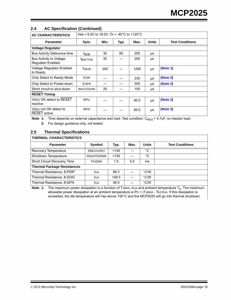
2.5 Thermal Specifications
Voltage Regulator
Bus Activity Debounce time tBDB 30 80 250 µs
Bus Activity to Voltage Regulator Enabled
tBACTIVE 35 — 200 µs
Voltage Regulator Enabled to Ready
tVEVR 300 — 1200 µs (Note 1)
Chip Select to Ready Mode tCSR — — 230 µs (Note 2)
Chip Select to Power-down tCSPD — — 300 µs (Note 2)
Short circuit to shut-down tSHUTDOWN 20 — 100 µs
RESET Timing
VREG OK detect to RESET inactive
tRPU — — 60.0 µs (Note 2)
VREG not OK detect to RESET active
tRPD — — 60.0 µs (Note 2)
Note 1: Time depends on external capacitance and load. Test condition: CREG = 4.7uF, no resistor load.
2: For design guidance only, not tested.
THERMAL CHARACTERISTICS
Parameter Symbol Typ. Max. Units Test Conditions
Recovery Temperature RECOVERY +140 — C
Shutdown Temperature SHUTDOWN +150 — C
Short Circuit Recovery Time tTHERM 1.5 5.0 ms
Thermal Package Resistances
Thermal Resistance, 8-PDIP JA 89.3 — C/W
Thermal Resistance, 8-SOIC JA 149.5 — C/W
Thermal Resistance, 8-QFN JA 48.0 — C/W
Note 1: The maximum power dissipation is a function of TJMAX, JA and ambient temperature TA. The maximum allowable power dissipation at an ambient temperature is PD = (TJMAX - TA)JA. If this dissipation is exceeded, the die temperature will rise above 150C and the MCP2025 will go into thermal shutdown.
2.4 AC Specification (Continued)
AC CHARACTERISTICS VBB = 6.0V to 18.0V; TA = -40°C to +125°C
Parameter Sym. Min. Typ. Max. Units Test Conditions
2012 Microchip Technology Inc. DS22306A-page 19
MCP2025
2.6 Timing Diagrams and Specifications
FIGURE 2-2: BUS TIMING DIAGRAM
FIGURE 2-3: REGULATOR BUS WAKE TIMING DIAGRAM
.95VLBUS
.05VLBUS
tTRANSPDR
tRECPDR
tTRANSPDF
tRECPDF
TXD
LBUS
RXD
50%50%
.50VBB
50%50%
0.0V
VREG
LBUS
VWK(LBUS)
tVEVR
VREG-NOM
tBDBtBACTIVE
DS22306A-page 20 2012 Microchip Technology Inc.
MCP2025
FIGURE 2-4: CS/LWAKE, REGULATOR AND RESET TIMING DIAGRAM
FIGURE 2-5: TYPICAL IBBQ VS. TEMPERATURE - 5.0V
FIGURE 2-6: IBBQ TRANS-OFF VS. TEMPERATURE - 5.0V
FIGURE 2-7: IBBQ POWER-DOWN VS. TEMPERATURE - 5.0V
tCSPD
tCSR
CS/LWAKE
VREG
VREG-NOM
RESET
tRPU
tVEVR
tRPD
020406080
100120140160180
-45 -10 25 90 130
6V12V18V
Temperature(⁰C)
IBB
Q(μ
A)
0
10
20
30
40
50
60
70
80
-45 -10 25 90 130
6V12V18V
Temperature(⁰C)
IBB
Q(μ
A)
0
1
2
3
4
5
6
-45 -10 25 90 130
6V
12V
18V
Temperature(⁰C)
IBB
Q(μ
A)
2012 Microchip Technology Inc. DS22306A-page 21
MCP2025
FIGURE 2-8: TYPICAL IBBQVS. TEMPERATURE - 3.3V
FIGURE 2-9: IBBQ TRANS-OFF VS. TEMPERATURE - 3.3V
FIGURE 2-10: IBBQ POWER-DOWN VS. TEMPERATURE - 3.3V
020406080
100120140160180200
-45 -10 25 90 130
6V
12V
18V
IBB
Q(μ
A)
Temperature(⁰C)
0102030405060708090
-45 -10 25 90 130
6V
12V
18V
Temperature(⁰C)
IBB
Q(μ
A)
0
1
2
3
4
5
6
-45 -10 25 90 130
6V12V18V
IBB
Q(μ
A)
Temperature(⁰C)
DS22306A-page 22 2012 Microchip Technology Inc.
MCP2025
3.0 PACKAGING INFORMATION
3.1 Package Marking Information
Legend: XX...X Customer-specific informationY Year code (last digit of calendar year)YY Year code (last 2 digits of calendar year)WW Week code (week of January 1 is week ‘01’)NNN Alphanumeric traceability code Pb-free JEDEC designator for Matte Tin (Sn)* This package is Pb-free. The Pb-free JEDEC designator ( )
can be found on the outer packaging for this package.
Note: In the event the full Microchip part number cannot be marked on one line, it willbe carried over to the next line, thus limiting the number of availablecharacters for customer-specific information.
3e
3e
NNN
8-Lead SOIC (150 mil) Example:
2025-500E/SN1220
256
XXXXXXXXXXXXXNNN
YYWW
8-Lead PDIP (300 mil) Example
YYWWNNN
XXXXXXXXXXXX
PIN 1 PIN 1
202550E/MD ^^
1220256
8-Lead DFN (4x4x0.9 mm) Example
2025500E/P ^^256
12203e
3e
2012 Microchip Technology Inc. DS22306A-page 23
MCP2025
8-Lead Plastic Dual Flat, No Lead Package (MD) 4x4x0.9 mm Body [DFN]
Note: For the most current package drawings, please see the Microchip Packaging Specification located at http://www.microchip.com/packaging
Microchip Technology Drawing C04-131E Sheet 1 of 2
DS22306A-page 24 2012 Microchip Technology Inc.
MCP2025
8-Lead Plastic Dual Flat, No Lead Package (MD) 4x4x0.9 mm Body [DFN]
Note: For the most current package drawings, please see the Microchip Packaging Specification located at http://www.microchip.com/packaging
Microchip Technology Drawing C04-131E Sheet 2 of 2
2012 Microchip Technology Inc. DS22306A-page 25
MCP2025
Note: For the most current package drawings, please see the Microchip Packaging Specification located at http://www.microchip.com/packaging
DS22306A-page 26 2012 Microchip Technology Inc.
MCP2025
!"#$%&"' ()"&'"!&)&#*&&&# +%&,&!&- '!!#.#&"#'#%!&"!!#%!&"!!!&$#/!# '!#&.0
1,21!'! &$& "!**&"&&!
3&'!&"&4#*!(!!&4%&&#&&&255***''54
6&! 7,8.'!9'&! 7 7: ;
7"')%! 7 <& 1, && = = ##4 4!! - 1!&& = ="#&"#>#& . - -##4>#& . <: 9& -< -? && 9 - 9# 4!! < 69#>#& ) ? 9*9#>#& ) < : *+ 1 = = -
N
E1
NOTE 1
D
1 2 3
A
A1
A2
L
b1b
e
E
eB
c
* ,<1
2012 Microchip Technology Inc. DS22306A-page 27
MCP2025
Note: For the most current package drawings, please see the Microchip Packaging Specification located at http://www.microchip.com/packaging
DS22306A-page 28 2012 Microchip Technology Inc.
MCP2025
Note: For the most current package drawings, please see the Microchip Packaging Specification located at http://www.microchip.com/packaging
2012 Microchip Technology Inc. DS22306A-page 29
MCP2025
! ""#$%& !'
3&'!&"&4#*!(!!&4%&&#&&&255***''54
DS22306A-page 30 2012 Microchip Technology Inc.
MCP2025
APPENDIX A: REVISION HISTORY
Revision A (June 2012)
• Original Release of this Document.
2012 Microchip Technology Inc. DS22306A-page 31
MCP2025
NOTES:
DS22306A-page 32 2012 Microchip Technology Inc.
MCP2025
PRODUCT IDENTIFICATION SYSTEM
To order or obtain information, e.g., on pricing or delivery, refer to the factory or the listed sales office.
Device: MCP2025: LIN Transceiver with Voltage RegulatorMCP2025T: LIN Transceiver with Voltage Regulator
(Tape and Reel) (SOIC and DFN only)
Temperature Range: E = -40°C to +125°C
Package: P = Plastic DIP (300 mil Body), 8-leadSN = Plastic Small Outline SOIC, 8-leadMD = Plastic Dual Flat DFN, 8-lead
PART NO. –X /XX
PackageTemperatureRange
Device
Examples:
a) MCP2025-330E/SN: 3.3V, 8L-SOIC package
b) MCP2025-330E/P: 3.3V, 8L-PDIP package
c) MCP2025-330E/MD: 3.3V, 8L-DFN package
d) MCP2025-500E/SN: 5.0V, 8L-SOIC package
e) MCP2025-500E/P: 5.0V, 8L-PDIP package
f) MCP2025-500E/MD: 5.0V, 8L-DFN package
g) MCP2025T-330E/SN: Tape and Reel,3.3V, 8L-SOIC package
h) MCP2025T-500E/SN: Tape and Reel,5.0V, 8L-SOIC package
i) MCP2025T-330E/MD: Tape and Reel,3.3V, 8L-DFN package
j) MCP2025T-500E/MD: Tape and Reel,5.0V, 8L-DFN package
2012 Microchip Technology Inc. DS22306A-page 33

MCP2025
NOTES:
DS22306A-page 34 2012 Microchip Technology Inc.
Note the following details of the code protection feature on Microchip devices:
• Microchip products meet the specification contained in their particular Microchip Data Sheet.
• Microchip believes that its family of products is one of the most secure families of its kind on the market today, when used in the intended manner and under normal conditions.
• There are dishonest and possibly illegal methods used to breach the code protection feature. All of these methods, to our knowledge, require using the Microchip products in a manner outside the operating specifications contained in Microchip’s Data Sheets. Most likely, the person doing so is engaged in theft of intellectual property.
• Microchip is willing to work with the customer who is concerned about the integrity of their code.
• Neither Microchip nor any other semiconductor manufacturer can guarantee the security of their code. Code protection does not mean that we are guaranteeing the product as “unbreakable.”
Code protection is constantly evolving. We at Microchip are committed to continuously improving the code protection features of ourproducts. Attempts to break Microchip’s code protection feature may be a violation of the Digital Millennium Copyright Act. If such actsallow unauthorized access to your software or other copyrighted work, you may have a right to sue for relief under that Act.
Information contained in this publication regarding deviceapplications and the like is provided only for your convenienceand may be superseded by updates. It is your responsibility toensure that your application meets with your specifications.MICROCHIP MAKES NO REPRESENTATIONS ORWARRANTIES OF ANY KIND WHETHER EXPRESS ORIMPLIED, WRITTEN OR ORAL, STATUTORY OROTHERWISE, RELATED TO THE INFORMATION,INCLUDING BUT NOT LIMITED TO ITS CONDITION,QUALITY, PERFORMANCE, MERCHANTABILITY ORFITNESS FOR PURPOSE. Microchip disclaims all liabilityarising from this information and its use. Use of Microchipdevices in life support and/or safety applications is entirely atthe buyer’s risk, and the buyer agrees to defend, indemnify andhold harmless Microchip from any and all damages, claims,suits, or expenses resulting from such use. No licenses areconveyed, implicitly or otherwise, under any Microchipintellectual property rights.
2012 Microchip Technology Inc.
QUALITY MANAGEMENT SYSTEM CERTIFIED BY DNV
== ISO/TS 16949 ==
Trademarks
The Microchip name and logo, the Microchip logo, dsPIC, KEELOQ, KEELOQ logo, MPLAB, PIC, PICmicro, PICSTART, PIC32 logo, rfPIC and UNI/O are registered trademarks of Microchip Technology Incorporated in the U.S.A. and other countries.
FilterLab, Hampshire, HI-TECH C, Linear Active Thermistor, MXDEV, MXLAB, SEEVAL and The Embedded Control Solutions Company are registered trademarks of Microchip Technology Incorporated in the U.S.A.
Analog-for-the-Digital Age, Application Maestro, chipKIT, chipKIT logo, CodeGuard, dsPICDEM, dsPICDEM.net, dsPICworks, dsSPEAK, ECAN, ECONOMONITOR, FanSense, HI-TIDE, In-Circuit Serial Programming, ICSP, Mindi, MiWi, MPASM, MPLAB Certified logo, MPLIB, MPLINK, mTouch, Omniscient Code Generation, PICC, PICC-18, PICDEM, PICDEM.net, PICkit, PICtail, REAL ICE, rfLAB, Select Mode, Total Endurance, TSHARC, UniWinDriver, WiperLock and ZENA are trademarks of Microchip Technology Incorporated in the U.S.A. and other countries.
SQTP is a service mark of Microchip Technology Incorporated in the U.S.A.
All other trademarks mentioned herein are property of their respective companies.
© 2012, Microchip Technology Incorporated, Printed in the U.S.A., All Rights Reserved.
Printed on recycled paper.
ISBN: 978-1-62076-393-3
DS22306A-page 35
Microchip received ISO/TS-16949:2009 certification for its worldwide headquarters, design and wafer fabrication facilities in Chandler and Tempe, Arizona; Gresham, Oregon and design centers in California and India. The Company’s quality system processes and procedures are for its PIC® MCUs and dsPIC® DSCs, KEELOQ® code hopping devices, Serial EEPROMs, microperipherals, nonvolatile memory and analog products. In addition, Microchip’s quality system for the design and manufacture of development systems is ISO 9001:2000 certified.
DS22306A-page 36 2012 Microchip Technology Inc.
AMERICASCorporate Office2355 West Chandler Blvd.Chandler, AZ 85224-6199Tel: 480-792-7200 Fax: 480-792-7277Technical Support: http://www.microchip.com/supportWeb Address: www.microchip.com
AtlantaDuluth, GA Tel: 678-957-9614 Fax: 678-957-1455
BostonWestborough, MA Tel: 774-760-0087 Fax: 774-760-0088
ChicagoItasca, IL Tel: 630-285-0071 Fax: 630-285-0075
ClevelandIndependence, OH Tel: 216-447-0464 Fax: 216-447-0643
DallasAddison, TX Tel: 972-818-7423 Fax: 972-818-2924
DetroitFarmington Hills, MI Tel: 248-538-2250Fax: 248-538-2260
IndianapolisNoblesville, IN Tel: 317-773-8323Fax: 317-773-5453
Los AngelesMission Viejo, CA Tel: 949-462-9523 Fax: 949-462-9608
Santa ClaraSanta Clara, CA Tel: 408-961-6444Fax: 408-961-6445
TorontoMississauga, Ontario, CanadaTel: 905-673-0699 Fax: 905-673-6509
ASIA/PACIFICAsia Pacific OfficeSuites 3707-14, 37th FloorTower 6, The GatewayHarbour City, KowloonHong KongTel: 852-2401-1200Fax: 852-2401-3431
Australia - SydneyTel: 61-2-9868-6733Fax: 61-2-9868-6755
China - BeijingTel: 86-10-8569-7000 Fax: 86-10-8528-2104
China - ChengduTel: 86-28-8665-5511Fax: 86-28-8665-7889
China - ChongqingTel: 86-23-8980-9588Fax: 86-23-8980-9500
China - HangzhouTel: 86-571-2819-3187 Fax: 86-571-2819-3189
China - Hong Kong SARTel: 852-2401-1200 Fax: 852-2401-3431
China - NanjingTel: 86-25-8473-2460Fax: 86-25-8473-2470
China - QingdaoTel: 86-532-8502-7355Fax: 86-532-8502-7205
China - ShanghaiTel: 86-21-5407-5533 Fax: 86-21-5407-5066
China - ShenyangTel: 86-24-2334-2829Fax: 86-24-2334-2393
China - ShenzhenTel: 86-755-8203-2660 Fax: 86-755-8203-1760
China - WuhanTel: 86-27-5980-5300Fax: 86-27-5980-5118
China - XianTel: 86-29-8833-7252Fax: 86-29-8833-7256
China - XiamenTel: 86-592-2388138 Fax: 86-592-2388130
China - ZhuhaiTel: 86-756-3210040 Fax: 86-756-3210049
ASIA/PACIFICIndia - BangaloreTel: 91-80-3090-4444 Fax: 91-80-3090-4123
India - New DelhiTel: 91-11-4160-8631Fax: 91-11-4160-8632
India - PuneTel: 91-20-2566-1512Fax: 91-20-2566-1513
Japan - OsakaTel: 81-66-152-7160 Fax: 81-66-152-9310
Japan - YokohamaTel: 81-45-471- 6166 Fax: 81-45-471-6122
Korea - DaeguTel: 82-53-744-4301Fax: 82-53-744-4302
Korea - SeoulTel: 82-2-554-7200Fax: 82-2-558-5932 or 82-2-558-5934
Malaysia - Kuala LumpurTel: 60-3-6201-9857Fax: 60-3-6201-9859
Malaysia - PenangTel: 60-4-227-8870Fax: 60-4-227-4068
Philippines - ManilaTel: 63-2-634-9065Fax: 63-2-634-9069
SingaporeTel: 65-6334-8870Fax: 65-6334-8850
Taiwan - Hsin ChuTel: 886-3-5778-366Fax: 886-3-5770-955
Taiwan - KaohsiungTel: 886-7-536-4818Fax: 886-7-330-9305
Taiwan - TaipeiTel: 886-2-2500-6610 Fax: 886-2-2508-0102
Thailand - BangkokTel: 66-2-694-1351Fax: 66-2-694-1350
EUROPEAustria - WelsTel: 43-7242-2244-39Fax: 43-7242-2244-393Denmark - CopenhagenTel: 45-4450-2828 Fax: 45-4485-2829
France - ParisTel: 33-1-69-53-63-20 Fax: 33-1-69-30-90-79
Germany - MunichTel: 49-89-627-144-0 Fax: 49-89-627-144-44
Italy - Milan Tel: 39-0331-742611 Fax: 39-0331-466781
Netherlands - DrunenTel: 31-416-690399 Fax: 31-416-690340
Spain - MadridTel: 34-91-708-08-90Fax: 34-91-708-08-91
UK - WokinghamTel: 44-118-921-5869Fax: 44-118-921-5820
Worldwide Sales and Service
11/29/11


![TJA1028 LIN transceiver with integrated voltage regulator · PDF fileTJA1028TK/xxx/xx[1][2] ... According to the Open System Interconnect (OSI) model, these modules make up the LIN](https://img.pdfslide.us/doc/110x75/5ab1a4b17f8b9a284c8cc8f8/tja1028-lin-transceiver-with-integrated-voltage-regulator-12-according-to.jpg)