Embed Size (px)
Citation preview
ANRV320-AA45-03 ARI 24 July 2007 18:32
Infrared Detector Arraysfor AstronomyG.H. RiekeSteward Observatory, University of Arizona, Tucson, Arizona 85750;email: [email protected]
Annu. Rev. Astron. Astrophys. 2007. 45:77–115
First published online as a Review in Advance onMay 21, 2007.
The Annual Review of Astronomy and Astrophysics isonline at astro.annualreviews.org
This article’s doi:10.1146/annurev.astro.44.051905.092436
Copyright c© 2007 by Annual Reviews.All rights reserved
0066-4146/07/0922-0077$20.00
Key Words
astronomical techniques, bolometers, photoconducting devices,photodiodes, impurity band conduction (IBC) detectors
AbstractUse of infrared detector arrays in astronomy began roughly 20 yearsago, and our detection capabilities in parts of this spectral rangehave doubled about every seven months since then. A variety ofapproaches are now used for detector arrays operating from 1 μmto 1 mm and beyond. They include direct hybrid arrays of InSb andHgCdTe photodiodes that operate from 0.6 μm to 5 μm, and of Si:Asimpurity band conduction detectors from 5 μm to 28 μm; a numberof approaches to photoconductive detector arrays in the far-infrared;and bolometer arrays read out by transistors or superconductingdevices in the far-infrared through millimeter-wave spectral range.The underlying principles behind these approaches are discussed.The application of these principles is illustrated through detaileddiscussion of a number of state-of-the-art detector arrays.
77
Ann
u. R
ev. A
stro
. Ast
roph
ys. 2
007.
45:7
7-11
5. D
ownl
oade
d fr
om w
ww
.ann
ualr
evie
ws.
org
by C
alif
orni
a In
stitu
te o
f T
echn
olog
y on
11/
09/1
2. F
or p
erso
nal u
se o
nly.
ANRV320-AA45-03 ARI 24 July 2007 18:32
RVS: Raytheon VisionSystems
1. INTRODUCTION
We have many ways to detect photons. In selecting one of these options, most usersfeel constrained by practical considerations such as ruggedness and convenience.However, astronomers are nearly unique in the demands they make to approachfundamental levels of performance. For them, how quickly a detection can be achievedon faint sources is virtually all that matters. This behavior depends on a combination ofdetector characteristics such as (a) noise, (b) quantum efficiency and (c) the number ofpixels that can be put into an array. Together, they can be gauged by the astronomicalcapability metric (Bahcall et al. 1991), which is proportional to
(# of pixels) × (sensitivity per pixel )2. (1)
This metric indicates the number of positions on the sky that can be measured in agiven time to a given detection limit. A similar expression applies for spectroscopy(where for a simple spectrograph, the free spectral range and slit length substitute forpositions on the sky).
The foundations of modern infrared astronomy were laid in 1965–1985, basedon observations with single detectors (or small collections of such detectors operatedin parallel) (Low, Rieke & Gehrz 2007). The first astronomical use of true infrareddetector arrays occurred about 20 years ago (e.g., Arens et al. 1984, Forrest et al.1985). These early devices were small (typically 32 × 32 pixels) with read noises ofmore than 1000 electrons. They were described as having performance similar to thatof the best single-pixel devices, but with the multiple-pixel advantages of an array (seeWynn-Williams & Becklin 1987 for a number of articles on early infrared arrays forastronomy). Starting just before these first demonstrations, the astronomical capabil-ity for near-infrared detection as measured by Equation 1 has doubled roughly everyseven months.
Astronomers can only take a little credit for the incredible expansion of capabili-ties in the near- and mid-infrared (1 μm to 5 μm and 5 μm to 30 μm, respectively).The initial investments that established the basic architecture and processes to pro-duce high-performance arrays came from the military (e.g., Harwit 2000). Furtherinvestments from NASA and the National Science Foundation have allowed the de-velopment of the incredible devices to be described below. The array manufacturershave taken a strong interest and have done far more for us than we might haveanticipated. Some of these groups have been disbanded, but we must express ourappreciation to the ones that are still developing improved detector arrays. They areRaytheon Vision Systems (RVS), DRS Technologies, and Teledyne Imaging Sensors(formerly Rockwell Scientific Company; the names occasionally change as a result ofcorporate reorganizations and acquisitions). In the far-infrared (30 μm to 200 μm)and submillimeter (200 μm to 1000 μm), however, astronomy has often been themajor customer for detector arrays and astronomers have played far more centralroles in developing the fundamental technologies.
This review first discusses hybrid infrared detector arrays operating from 0.6through 120 μm. It describes the building blocks for these devices: Section 2 examinesthe detectors themselves; Section 3 examines the readouts; and Section 4 examines
78 Rieke
Ann
u. R
ev. A
stro
. Ast
roph
ys. 2
007.
45:7
7-11
5. D
ownl
oade
d fr
om w
ww
.ann
ualr
evie
ws.
org
by C
alif
orni
a In
stitu
te o
f T
echn
olog
y on
11/
09/1
2. F
or p
erso
nal u
se o
nly.
ANRV320-AA45-03 ARI 24 July 2007 18:32
the process to join the detectors and readouts together. Further discussion of thesematters can be found in Rieke (2003). Section 5 discusses a few examples of state-of-the-art arrays. Section 6 describes bolometer arrays being constructed for therange from ∼50 μm to the millimeter-wave. Richards & McCreight (2005) provide ashorter review of all these topics that also gives more background information. Section7 describes some aspects of the detailed performance of these devices, and Section 8summarizes and illustrates briefly the impact of arrays on infrared astronomy.
2. DETECTORS
Detector arrays for the near- and mid-infrared detect photons through some form ofphotoconductivity. The most fundamental photoconductive detector is a small blockof semiconductor material with electrodes on opposite faces that are used to establishan electric field within the material volume. When photons free charge carriers withinthe block, the carriers migrate toward the electrodes and produce a current that can besensed by a high-performance amplifier. When the photon energy is at least as largeas the binding energy of the electrons in the semiconductor crystal, detection occursthrough intrinsic photoconductivity, where the charge carriers are freed by breakinga semiconductor crystal bond. In the language of solid state physics, an electron ispromoted from the valence energy band across the band gap to the conduction energyband. Detectors based on intrinsic absorption can operate up to a cutoff wavelength,λc, corresponding to the band gap energy of the material, or
λc = hcEg
= 1.24 μmEg (eV)
, (2)
where h is Planck’s constant, c is the speed of light, and Eg is the band gap energy. Forexample, InSb has a band gap of ∼0.22 eV at 77 K and hence λc ∼ 5.6 μm.
Detectors can also be based on extrinsic photoconductivity. Here, a photon freesa charge carrier by interacting with an impurity atom within the semiconductor crys-tal. In the language of solid state physics, an electron may get elevated from thevalence band to an impurity level to create a hole (a missing negative charge thatcan be described as if it were a positively charged particle). Alternatively, an elec-tron may be freed by elevating it from an impurity level to the conduction band.Either the hole or the electron can then move through the material in responseto the electric field in the detector. The advantage of detectors based on extrin-sic photoconductivity is that they can operate to much longer wavelengths, becauseit takes less energy to free a charge carrier from an impurity atom than from anatom of the semiconductor crystal material. The necessary photon energy corre-sponds to the energy difference between the impurity level and either the top ofthe valence band or bottom of the conduction one. That is, the gap energy, Eg, inEquation 2 can be replaced by the smaller impurity ionization energy Ei. Intrinsicphotoconductivity is a very efficient process because the absorption of photons isstrong and therefore high quantum efficiency (the proportion of photons convertedto detectable charge carriers) can be achieved in thin layers of material. Extrinsicphotoconductivity is far less efficient because of limits in the amount of impurity that
www.annualreviews.org • Infrared Detector Arrays 79
Ann
u. R
ev. A
stro
. Ast
roph
ys. 2
007.
45:7
7-11
5. D
ownl
oade
d fr
om w
ww
.ann
ualr
evie
ws.
org
by C
alif
orni
a In
stitu
te o
f T
echn
olog
y on
11/
09/1
2. F
or p
erso
nal u
se o
nly.
ANRV320-AA45-03 ARI 24 July 2007 18:32
can be introduced into the semiconductor without altering the nature of the impuritystates.
Implicit in the treatment of low background detectors is that the generation offree charge carriers is dominated by photon absorption, not by thermal excitation.Lower temperature is required for this condition as the long wavelength cutoff of thedetector increases, going approximately as (see Hoffman, Love & Rosbeck 2004)
Tmax = 200 Kλc (μm)
. (3)
Second-order effects, such as construction of the detector as a photodiode with ahigh impedance depletion zone, can relax the temperature requirements, but onlymodestly.
For a simple, or bulk, photoconductor, the identical block of semiconductor mustmeet both the electrical and optical requirements. Conflicts in these requirementscan limit the detector performance. The most fundamental electrical parameter isresistance, R. The thermally driven Brownian motion of charge carriers generates afluctuating electrical current that produces Johnson (1928) noise:
⟨I 2J
⟩1/2 =√
4kT dfR
, (4)
where k is Boltzmann’s constant, T is the absolute temperature, and df is the frequencybandwidth of the electrical apparatus. Assuming the detector is cooled only to the levelrequired by Equation 3, the resistance required to suppress this noise to an acceptablelevel can be very high. If the impurity concentration in an extrinsic detector is toohigh, quantum mechanical processes such as tunneling and hopping allow chargeconduction (dark current) in the detector, reducing its resistance in ways that areimmune to mitigation by further reduction of the operating temperature.
The low levels of impurity concentration permitted by the electrical requirementsnecessitate long absorption paths for reasonable quantum efficiency. The resultingdetectors have high susceptibility to ionizing particles because of their large volumes.In addition, they are built with an electrode on each side of a high resistance dielectricdetector volume. The capacitance of this structure can interfere with the performanceas a detector. For example, when a charge is collected at one electrode, the needto inject a charge at the opposite electrode to maintain electrical neutrality is onlyconveyed at the speed of the dielectric time constant. This parameter is basically theRC time constant of the detector, which can be many seconds in a high performancedetector operating at low background (such as on a cooled telescope in space).
An unavoidable consequence, then, of the combined requirements for photonabsorption and high electrical resistance is that bulk extrinsic photoconductors at lowbackgrounds nearly always are operating out of electrical equilibrium. Consequently,their outputs consist of a fast component associated with the immediate release offree charge carriers by absorbed photons, plus a slow component that reflects theadjustment of the detector to the new interior condition imposed by the motion ofthe charge carriers. This behavior is sometimes described as a memory effect forpreviously detected sources. For similar reasons, the response of these devices is
80 Rieke
Ann
u. R
ev. A
stro
. Ast
roph
ys. 2
007.
45:7
7-11
5. D
ownl
oade
d fr
om w
ww
.ann
ualr
evie
ws.
org
by C
alif
orni
a In
stitu
te o
f T
echn
olog
y on
11/
09/1
2. F
or p
erso
nal u
se o
nly.
ANRV320-AA45-03 ARI 24 July 2007 18:32
IRAS: Infrared AstronomicalSatellite
ISO: Infrared SpaceObservatory
modified when a cosmic ray (or other ionizing particle) creates a flood of chargewithin them. These effects obviously are a challenge for calibration. Nonetheless,such detectors have been used in the Infrared Astronomical Satellite (IRAS), the InfraredSpace Observatory (ISO), and for the far-infrared channels on the Spitzer Space Telescope(Spitzer). In the latter case, rather elaborate strategies both in the instrument and inthe data pipeline have tamed the calibration problems to a large extent.
In addition, there are inherent contradictions in the optical and electrical parame-ters of some semiconductors with otherwise desirable characteristics for bulk intrinsicphotoconductive detectors. For example, InSb has large electron mobility, making itimpossible to achieve high resistance in a geometry that allows for a reasonable biasvoltage and good quantum efficiency.
The solution is to separate the electrical and optical functions of the device. Virtu-ally all detectors operating between 1 μm and 5 μm are based on this approach. Highperformance detectors are manufactured as photodiodes in InSb and other semicon-ductors by forming a junction, with one side doped with donor impurities (n-type)and the other doped with acceptors (p-type). An n-type impurity has an additionalelectron beyond those needed to complete the crystal bonds, whereas a p-type im-purity has one less electron than needed for these bonds. Because the extra electronsare relatively easily freed from the donor atoms, close to the junction they flow to theacceptors and bond with them to complete the crystal structure. As a result, there is anet positive voltage on the donor side and negative voltage on the acceptor side of thejunction. The net voltage across the junction is called the contact voltage. It createsa contact potential field that sweeps any free charge carriers across the junction anddepletes this region of them, causing it to have high resistance. Photons are absorbedin the material in the vicinity of the junction and produce free charge carriers thatdiffuse toward it; when they fall into the junction field, they are driven across the junc-tion and produce a current. Because the photons have sufficient energy for intrinsicabsorption, the absorption is efficient. To preserve the potential for high quantum ef-ficiency, the absorbing layer must be thin enough for the diffusion to occur much morequickly than the carrier lifetime. Assuming this condition is met, quantum efficienciesapproaching 100% can be obtained in devices coated to minimize reflection losses.
InSb was the first material used widely in high-performance near-infrared pho-todiodes. Its band gap at 77 K provides response out to about 5.6 μm (with a slightdependence on operating temperature, e.g., a cutoff at 5.2 μm at 2 K), thus nicelymatching the JHKLM atmospheric windows. The material can be grown with goodcrystallography, high purity, and excellent uniformity, all of which contribute to itshigh performance in infrared detectors (Hoffman et al. 2004).
In addition to InSb, Hg(1−x)CdxTe is used widely for photodiodes. By varying theelemental composition of this material, the band gap can be changed from 1.55 eV forx = 1, corresponding to a cutoff wavelength of 0.8 μm, to a very small band gap energy,or even a metal. For years, this flexibility in the band gap was the main advantage ofHgCdTe for detectors compared with simple semiconductors such as InSb. It madeit possible to relax the detector cooling requirements when response was requiredonly at wavelengths less than 5.6 μm (Equation 3). Early methods for manufacturingHgCdTe material had difficulties achieving the level of uniformity of InSb devices
www.annualreviews.org • Infrared Detector Arrays 81
Ann
u. R
ev. A
stro
. Ast
roph
ys. 2
007.
45:7
7-11
5. D
ownl
oade
d fr
om w
ww
.ann
ualr
evie
ws.
org
by C
alif
orni
a In
stitu
te o
f T
echn
olog
y on
11/
09/1
2. F
or p
erso
nal u
se o
nly.
ANRV320-AA45-03 ARI 24 July 2007 18:32
MBE: molecular beamepitaxy
with their inherently simpler material. However, superb HgCdTe detectors are nowproduced by Teledyne using molecular beam epitaxy (MBE; where the detector isbuilt up literally one molecular layer at a time from a molecular beam in vacuum)and by RVS using advanced liquid phase epitaxy (where the crystal is grown from aliquid in which the detector material has been introduced at high concentration). Thecontrol now achieved over the internal structure of the photodiodes (see Figure 1)allows adjustment of the molecular composition and, hence, the band gap withinthe detector to improve the performance (Garnett et al. 2004a). In practice, veryhigh-performance photodiodes with cutoff wavelengths in the 5 μm range can bemanufactured in either InSb or Hg0.70Cd0.30Te, with HgCdTe providing the potentialof even higher performance with relaxed temperature requirements where shortervalues of λc are acceptable—for example, Hg0.55Cd0.45Te provides λc ∼ 2.5 μm.
Because of its adjustable band gap, HgCdTe would seem to be the logical approachfor devices operating at wavelengths longer than 5 μm. The biggest issue is thatmaterial with a small band gap only allows a small contact voltage to maintain thediode depletion region. Therefore, long-wavelength detectors tend to have high darkcurrent. Promising results have been reported by Bacon et al. (2004) for HgCdTedetectors fabricated to have a cutoff wavelength of 9.6 μm and operating at 30 K.They found that half the pixels in the test array had dark current below 0.05 e/s; one-sixth of the pixels with the highest dark current still fell between 4 and 30 e/s. HgCdTediodes can be made to work reasonably well out to ∼15 μm, but with too much darkcurrent for the performance levels demanded by astronomers. If high-performancedetectors can be developed with cutoff wavelengths somewhat longer than at present(e.g., 13 μm would allow operation across the entire 10 μm atmospheric window),this technology would find wide application in astronomy.
Beyond 10 μm, excellent performance is achieved using a different approach toseparate the electrical and optical functions of extrinsic silicon detectors. These de-vices are termed impurity band conduction (IBC) detectors (see Figure 2). They havebeen built using Si:Ga (cutoff wavelength ∼18 μm; Hogue et al. 2003), Si:As (cutoffwavelength ∼28 μm—widely used on groundbased telescopes and in all three Spitzerinstruments), and with Si:Sb (cutoff ∼40 μm) for the Spitzer infrared spectrograph(Huffman et al. 1992, van Cleve et al. 1995). Phosphorus is another attractive dopant
−−−−−−−−−−−−−−−−−−−−−−−−−−−−−−−−−−−−−−−−−−−−−−−−−−−−−−−−−−−−−−→Figure 1(a) Cross-sectional drawing of a HgCdTe photodiode. The junction is at the interface betweenp- and n-type material. The cap layer is grown with a larger band gap than the infrared-activen-type layer. The CdZnTe substrate is used to support the array of diodes while they are beinggrown, but can be removed afterward. The lower panel (b) shows schematically how a photonis detected. It is absorbed in the layer of n-type material to produce an electron-hole pair, eachmember of which then diffuses through the material. If the absorbing layer thickness, l, issmall enough, the hole falls into the contact potential field, E, before it can recombine. It isthen driven across the depletion region, producing the current that is used for the act ofdetection. The width of the depletion region is exaggerated for clarity. The upper panel(a) is based on the discussion in Garnett et al. (2004a). The lower panel (b) is based on a figurein Rieke (2003), reproduced by permission of Cambridge University Press.
82 Rieke
Ann
u. R
ev. A
stro
. Ast
roph
ys. 2
007.
45:7
7-11
5. D
ownl
oade
d fr
om w
ww
.ann
ualr
evie
ws.
org
by C
alif
orni
a In
stitu
te o
f T
echn
olog
y on
11/
09/1
2. F
or p
erso
nal u
se o
nly.
ANRV320-AA45-03 ARI 24 July 2007 18:32
Photon
a
b
p-type implant
HgCdTe cap layer
n-type HgCdTe
Transparent contact
CdZnTe substrate
Metallization
CdTe passivation
–Vb
Hole
Depletion region
e–
E
l
www.annualreviews.org • Infrared Detector Arrays 83
Ann
u. R
ev. A
stro
. Ast
roph
ys. 2
007.
45:7
7-11
5. D
ownl
oade
d fr
om w
ww
.ann
ualr
evie
ws.
org
by C
alif
orni
a In
stitu
te o
f T
echn
olog
y on
11/
09/1
2. F
or p
erso
nal u
se o
nly.
ANRV320-AA45-03 ARI 24 July 2007 18:32
Blocking layer
Oxide
IR-activelayer
Bottom contactimplant
Transparentsubstrate
Top contactimplant
Pixel
Metallization
Metallization
Buried contactetch and implant
Free electron
+Vb
Photon
Photon
Ele
ctric
fiel
d DepletedDepletedDepleted
a
b
c
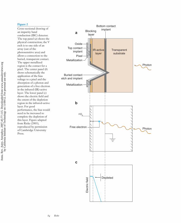
Figure 2Cross-sectional drawing ofan impurity bandconduction (IBC) detector.The top panel (a) shows thephysical construction; the Vetch is to one side of anarray (out of thephotosensitive area) andallows a connection to theburied, transparent contact.The upper metallizedregion is the contact for apixel. The center panel (b)shows schematically theapplication of the biasvoltage to a pixel and theabsorption of a photon andgeneration of a free electronin the infrared (IR)-activelayer. The lower panel (c)shows the electric field andthe extent of the depletionregion in the infrared-activelayer. For goodperformance, the bias wouldneed to be increased tocomplete the depletion ofthis layer. Figure adaptedfrom Rieke (2003),reproduced by permissionof Cambridge UniversityPress.
84 Rieke
Ann
u. R
ev. A
stro
. Ast
roph
ys. 2
007.
45:7
7-11
5. D
ownl
oade
d fr
om w
ww
.ann
ualr
evie
ws.
org
by C
alif
orni
a In
stitu
te o
f T
echn
olog
y on
11/
09/1
2. F
or p
erso
nal u
se o
nly.
ANRV320-AA45-03 ARI 24 July 2007 18:32
IBC: impurity bandconduction
CCD: charge coupleddevice
(cutoff ∼34 μm; Hogue et al. 2003) because it is widely used in commercial integratedcircuits and hence it would be relatively straightforward to fabricate detectors. IBCdetectors have also been fabricated with Ge:Ga (Watson & Huffman 1988), Ge:B (Wuet al. 1991), Ge:Sb (Bandaru, Beeman & Haller 2002), and GaAs:Te (Reichertz et al.2006), which together can extend this detector approach to beyond 300 μm. However,Si:As IBC detectors are the only form currently readily available in large format arrays.
The IBC detector in Figure 2 consists of a transparent silicon substrate, with aburied transparent contact and then a relatively heavily doped infrared-active layerof thickness 25 μm to 35 μm, followed by an intrinsic layer about 3 μm to 4 μmthick, with the second contact on this layer. The bias voltage on the buried contact isestablished through a V-shaped etched trough, metal-coated to make it conductive,and placed to one side of the array. Impurity band conductivity through hoppingin the active layer would produce unacceptable dark current if the infrared-activeband had access to both detector contacts. However, the impurity band terminates atthe blocking layer, so leakage can only occur through thermal excitation up into theconduction band (for this discussion, we assume an n-type dopant such as arsenic).Because the intrinsic layer blocks the dark current, the doping in the infrared-activelayer can be two orders of magnitude greater than in a bulk photoconductor, enoughto provide nearly complete absorption near the peak of the response. The highlydoped, thin active layer overcomes the issues with bulk detectors of slow adjustmenttoward electrical equilibrium and of large cross section for ionizing radiation.
The high conductivity of the infrared-active layer must be suppressed to make itpossible to generate a field across it and collect the photogenerated charge carriers.When a positive bias is applied across the blocking layer to the buried contact, negativecarriers are collected at the interface between the intrinsic and infrared-active layersand positive ones are driven away from this interface. Thus, a high-resistance regiondepleted of free charge carriers is produced in the infrared-active material near theinterface. However, beyond the depletion region there is virtually no field because ofthe high conductivity of this material. To gather photoelectrons efficiently that areproduced throughout this layer requires that it be entirely depleted. The minority,p-type impurities attach electrons and maintain a negative space charge in this regionthat tends to cancel the effect of the positive bias. Thus, complete depletion requiresthat the level of the minority impurities be kept very low, roughly below 2 × 1012 cm−3.That is, the impurity atoms must be at or below 1 in 1010 silicon atoms. As we discussin more detail below, high performance IBC detectors depend on material growthwith excellent minority impurity control.
3. READOUTS
Initially, infrared arrays used silicon charge coupled device (CCD) readouts. Thisapproach is not compatible with low read noise because of the low operating temper-ature required by the infrared detectors. Below about 70 K, the buried channels usedto avoid trapping noise in high performance CCDs freeze out—there is no longersufficient mobile charge to maintain the channel. The devices then operate in sur-face channel mode, with accompanying high noise. In addition, the sponsors for the
www.annualreviews.org • Infrared Detector Arrays 85
Ann
u. R
ev. A
stro
. Ast
roph
ys. 2
007.
45:7
7-11
5. D
ownl
oade
d fr
om w
ww
.ann
ualr
evie
ws.
org
by C
alif
orni
a In
stitu
te o
f T
echn
olog
y on
11/
09/1
2. F
or p
erso
nal u
se o
nly.
ANRV320-AA45-03 ARI 24 July 2007 18:32
MOSFET: metal oxidesemiconductor field effecttransistor
initial development of infrared arrays were worried about damage to the devices un-der extremely high doses of ionizing radiation, which can degrade the charge transferin CCDs. Therefore, a different architecture was developed in which a readout am-plifier is dedicated to each pixel, and transistor switches bring the signals to an outputamplifier. Ironically, the development of these devices to replace CCD readouts inthe infrared has come full circle with CMOS (complementary metal oxide semicon-ductor) detector arrays. They operate on the same amplifier-per-pixel basis and arereplacing CCDs in many applications in the optical (for a review of CMOS detectorarrays, see Hoffman, Loose & Suntharalingam 2005).
All modern near- and mid-infrared arrays have individual-amplifier-per-detectorreadouts based on metal oxide semiconductor field effect transistors (MOSFETs).MOSFETs are grown on a thin surface layer of a silicon substrate by laying downa pattern of insulators and conductors. They consist of a channel doped to allowcurrent flow between two electrodes, a source, and a drain. A third electrode, thegate, is placed on a thin insulator over the channel. Any current that deposits electriccharge onto the gate creates a field that modulates the current flow in the channel, thusamplifying the gate current. MOSFETs are the building block for integrated circuitsin general, and when run cold have nearly ideal properties for receiving the tinysignals from very high resistance infrared detectors. They require very little power,have virtually infinite input resistance, can be turned on and off without hysteresis,and can be constructed into very large and complex circuits.
In an infrared array, an individual detector amplifier collects the charge generatedby the detector on the combined capacitance of the detector and the MOSFET gate.The MOSFET amplifies this signal to provide enough drive power to convey it overcircuit traces for reasonable distances. The ensemble of readout MOSFETs directs
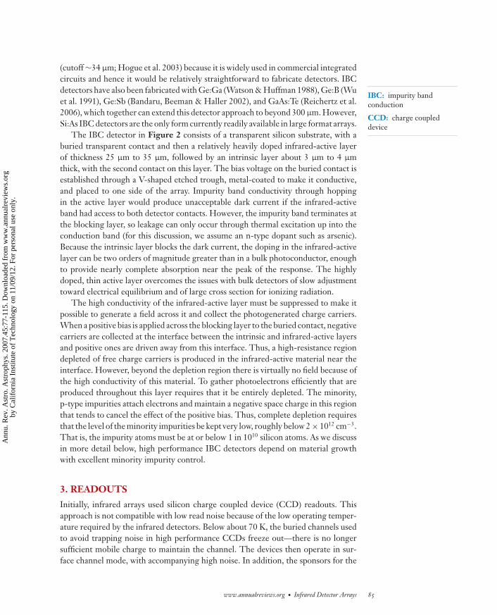
−−−−−−−−−−−−−−−−−−−−−−−−−−−−−−−−−−−−−−−−−−−−−−−−−−−−−−−−−−−−−−→Figure 3This figure shows a readout circuit—four cells of a detector array (the detectors are shownschematically as diodes). Signal is collected from the photodiode in the form of a current thatdeposits charge on the gate of transistor T1 until it is judged time to measure the integratedlevel of charge. To read it out, power is applied to the row driver R1 and, at the same time, toC1. The transistors T2, T3, and T4 conduct current as a result, and apply power to T1 as wellas connecting it to the output bus, which connects the signal to the output amplifier of thearray (lower left in the figure) where it can be measured with an external circuit. There is now achoice. If one wants to continue integrating the signal, power is removed from C1, and T2,T3, and T4 turn off, removing power from T1, so the pixel can continue to accumulate chargeon its gate. Possibly, power would be applied to C2 to read out the next pixel in the row of thearray. In any case, these steps provide a nondestructive read of the upper left pixel, becausethey allowed determination of the level of detected charge without disturbing it. In the secondcase, one resets the collected charge and initiates a new integration. To do so, the reset line(below the row bus in the figure) is pulsed while T2, T3, and T4 are still on, which sets theintegrating node (the input to T1) to the voltage VR. Because the integrated charge is lost inthis operation, and assuming one reads out T1 before the reset, this operation has caused adestructive read. It is therefore possible to address each pixel in the array individually, read outthe signal it has accumulated, and either continue through the array or reset the signal for anew integration. Figure from Rieke (2003), reproduced by permission of CambridgeUniversity Press.
86 Rieke
Ann
u. R
ev. A
stro
. Ast
roph
ys. 2
007.
45:7
7-11
5. D
ownl
oade
d fr
om w
ww
.ann
ualr
evie
ws.
org
by C
alif
orni
a In
stitu
te o
f T
echn
olog
y on
11/
09/1
2. F
or p
erso
nal u
se o
nly.
ANRV320-AA45-03 ARI 24 July 2007 18:32
ROIC: readout integratedcircuit
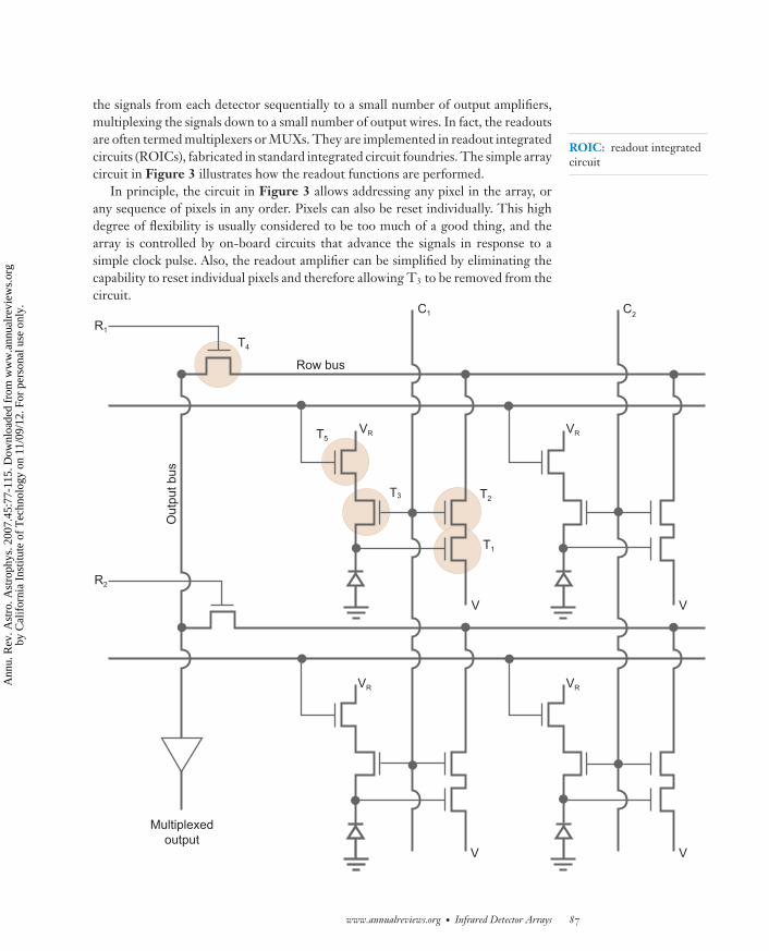
the signals from each detector sequentially to a small number of output amplifiers,multiplexing the signals down to a small number of output wires. In fact, the readoutsare often termed multiplexers or MUXs. They are implemented in readout integratedcircuits (ROICs), fabricated in standard integrated circuit foundries. The simple arraycircuit in Figure 3 illustrates how the readout functions are performed.
In principle, the circuit in Figure 3 allows addressing any pixel in the array, orany sequence of pixels in any order. Pixels can also be reset individually. This highdegree of flexibility is usually considered to be too much of a good thing, and thearray is controlled by on-board circuits that advance the signals in response to asimple clock pulse. Also, the readout amplifier can be simplified by eliminating thecapability to reset individual pixels and therefore allowing T3 to be removed from thecircuit.
Multiplexedoutput
R1
R2
T4
C1 C2
Row bus
Out
put b
us
T5
T3
T1
T2
VR VR
V V
VR
V
VR
V
www.annualreviews.org • Infrared Detector Arrays 87
Ann
u. R
ev. A
stro
. Ast
roph
ys. 2
007.
45:7
7-11
5. D
ownl
oade
d fr
om w
ww
.ann
ualr
evie
ws.
org
by C
alif
orni
a In
stitu
te o
f T
echn
olog
y on
11/
09/1
2. F
or p
erso
nal u
se o
nly.
ANRV320-AA45-03 ARI 24 July 2007 18:32
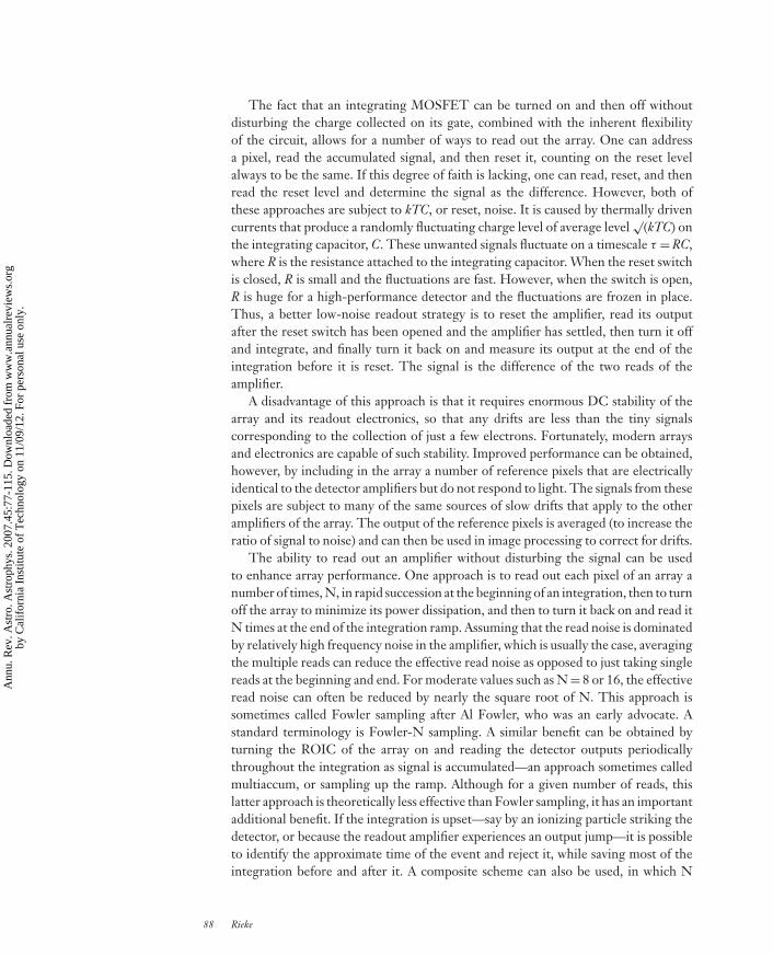
The fact that an integrating MOSFET can be turned on and then off withoutdisturbing the charge collected on its gate, combined with the inherent flexibilityof the circuit, allows for a number of ways to read out the array. One can addressa pixel, read the accumulated signal, and then reset it, counting on the reset levelalways to be the same. If this degree of faith is lacking, one can read, reset, and thenread the reset level and determine the signal as the difference. However, both ofthese approaches are subject to kTC, or reset, noise. It is caused by thermally drivencurrents that produce a randomly fluctuating charge level of average level
√(kTC) on
the integrating capacitor, C. These unwanted signals fluctuate on a timescale τ = RC,where R is the resistance attached to the integrating capacitor. When the reset switchis closed, R is small and the fluctuations are fast. However, when the switch is open,R is huge for a high-performance detector and the fluctuations are frozen in place.Thus, a better low-noise readout strategy is to reset the amplifier, read its outputafter the reset switch has been opened and the amplifier has settled, then turn it offand integrate, and finally turn it back on and measure its output at the end of theintegration before it is reset. The signal is the difference of the two reads of theamplifier.
A disadvantage of this approach is that it requires enormous DC stability of thearray and its readout electronics, so that any drifts are less than the tiny signalscorresponding to the collection of just a few electrons. Fortunately, modern arraysand electronics are capable of such stability. Improved performance can be obtained,however, by including in the array a number of reference pixels that are electricallyidentical to the detector amplifiers but do not respond to light. The signals from thesepixels are subject to many of the same sources of slow drifts that apply to the otheramplifiers of the array. The output of the reference pixels is averaged (to increase theratio of signal to noise) and can then be used in image processing to correct for drifts.
The ability to read out an amplifier without disturbing the signal can be usedto enhance array performance. One approach is to read out each pixel of an array anumber of times, N, in rapid succession at the beginning of an integration, then to turnoff the array to minimize its power dissipation, and then to turn it back on and read itN times at the end of the integration ramp. Assuming that the read noise is dominatedby relatively high frequency noise in the amplifier, which is usually the case, averagingthe multiple reads can reduce the effective read noise as opposed to just taking singlereads at the beginning and end. For moderate values such as N = 8 or 16, the effectiveread noise can often be reduced by nearly the square root of N. This approach issometimes called Fowler sampling after Al Fowler, who was an early advocate. Astandard terminology is Fowler-N sampling. A similar benefit can be obtained byturning the ROIC of the array on and reading the detector outputs periodicallythroughout the integration as signal is accumulated—an approach sometimes calledmultiaccum, or sampling up the ramp. Although for a given number of reads, thislatter approach is theoretically less effective than Fowler sampling, it has an importantadditional benefit. If the integration is upset—say by an ionizing particle striking thedetector, or because the readout amplifier experiences an output jump—it is possibleto identify the approximate time of the event and reject it, while saving most of theintegration before and after it. A composite scheme can also be used, in which N
88 Rieke
Ann
u. R
ev. A
stro
. Ast
roph
ys. 2
007.
45:7
7-11
5. D
ownl
oade
d fr
om w
ww
.ann
ualr
evie
ws.
org
by C
alif
orni
a In
stitu
te o
f T
echn
olog
y on
11/
09/1
2. F
or p
erso
nal u
se o
nly.
ANRV320-AA45-03 ARI 24 July 2007 18:32
repetitive reads are repeated in bursts throughout a sample-up-the-ramp integration.This latter approach can combine the benefits of both multiple read techniques.
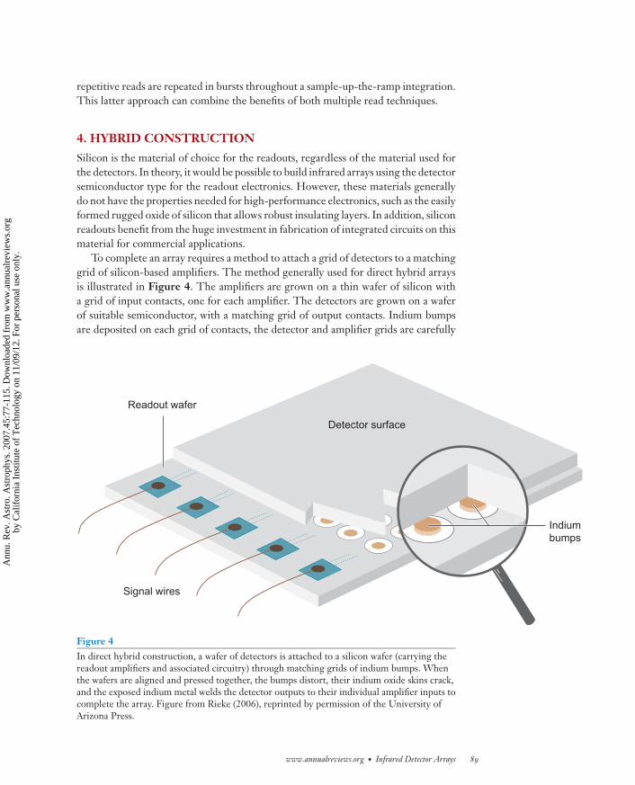
4. HYBRID CONSTRUCTION
Silicon is the material of choice for the readouts, regardless of the material used forthe detectors. In theory, it would be possible to build infrared arrays using the detectorsemiconductor type for the readout electronics. However, these materials generallydo not have the properties needed for high-performance electronics, such as the easilyformed rugged oxide of silicon that allows robust insulating layers. In addition, siliconreadouts benefit from the huge investment in fabrication of integrated circuits on thismaterial for commercial applications.
To complete an array requires a method to attach a grid of detectors to a matchinggrid of silicon-based amplifiers. The method generally used for direct hybrid arraysis illustrated in Figure 4. The amplifiers are grown on a thin wafer of silicon witha grid of input contacts, one for each amplifier. The detectors are grown on a waferof suitable semiconductor, with a matching grid of output contacts. Indium bumpsare deposited on each grid of contacts, the detector and amplifier grids are carefully
Signal wires
Readout wafer
Indiumbumps
Detector surface
Figure 4In direct hybrid construction, a wafer of detectors is attached to a silicon wafer (carrying thereadout amplifiers and associated circuitry) through matching grids of indium bumps. Whenthe wafers are aligned and pressed together, the bumps distort, their indium oxide skins crack,and the exposed indium metal welds the detector outputs to their individual amplifier inputs tocomplete the array. Figure from Rieke (2006), reprinted by permission of the University ofArizona Press.
www.annualreviews.org • Infrared Detector Arrays 89
Ann
u. R
ev. A
stro
. Ast
roph
ys. 2
007.
45:7
7-11
5. D
ownl
oade
d fr
om w
ww
.ann
ualr
evie
ws.
org
by C
alif
orni
a In
stitu
te o
f T
echn
olog
y on
11/
09/1
2. F
or p
erso
nal u
se o
nly.
ANRV320-AA45-03 ARI 24 July 2007 18:32
aligned, and a large force is applied to push them together. Indium is soft, and whenthe indium bumps deform, their indium oxide skins fracture and the exposed metalcold welds, attaching each detector to its matching amplifier. This process to producea many-pixel array is not simple because of the large forces that must be controlledprecisely, without the occurrence of sideways motion, and while maintaining theplanarity of the device. Another issue is that the thermal contraction of the detectormaterial on cooling generally differs from that of the readout (unless, of course,the detectors are made of silicon). The resulting forces can rip apart the indiumbump bonds, particularly at the corners of an array where the stresses are largestbecause the distance from the array center is largest. Something has to give. Toallow the necessary stretching, either the detector wafer is thinned (chemically, orby diamond-tool machining after the array has been hybridized), or the readout isthinned. Although it can readily be shown that typical detector materials would ripapart from their silicon readouts at an array size of about 1 cm square for rigidparts, arrays are now made up to about 3.6 cm2 (13 cm2 in area) with appropriatethinning.
5. ARRAY EXAMPLES
Teledyne/Rockwell and RVS supply the majority of infrared arrays used in astronomy;DRS Technologies fills nearly all the remainder of the market (Simons et al. 2006).The characteristics of the most advanced infrared arrays for astronomy from thesemanufacturers are summarized in Table 1. The parameters have been taken from avariety of sources without establishment of a common test protocol, so small differ-ences are not necessarily real. Operating conditions also influence the performancemeasures. For example, the DRS Technologies Si:As IBC array has been built to op-erate with solid hydrogen cryogen, so its dark current is a reflection of the relativelyhigh operating temperature for its detector type.
Even under nominally similar operating conditions, array performance may besubject to variations depending on test details. Hall (2006) illustrates how the TeledyneHAWAII-2RG is sensitive to temperature changes at the 1 mK level. With care tomaintain this level of stability, he finds that the read noise can be driven down to about4 electrons (Fowler-32 sampling) and the dark current to 0.002 e/s. The problem isthat such stability may be unachievable outside of the laboratory. Nonetheless, someof the benefits implied by these results can be achieved by operating arrays under themost uniform possible conditions. Specifically, the clocking cadences (the sequenceand timing of control signals to the array) should be kept extremely uniform and othersteps taken to maintain operating arrays in the most benign and constant environmentpossible.
Array performance is also strongly affected by background levels, whichcover a huge range for astronomical infrared arrays. Moderately high-resolution(λ/�λ ∼ 3000) spectrometers operating on the ground in the near-infrared betweenthe atmospheric airglow OH lines, or even more so in space, can deliver tiny back-ground signals of 0.1 photons/(s m2 arcsec2), or less for higher spectral resolution. An
90 Rieke
Ann
u. R
ev. A
stro
. Ast
roph
ys. 2
007.
45:7
7-11
5. D
ownl
oade
d fr
om w
ww
.ann
ualr
evie
ws.
org
by C
alif
orni
a In
stitu
te o
f T
echn
olog
y on
11/
09/1
2. F
or p
erso
nal u
se o
nly.
ANRV320-AA45-03 ARI 24 July 2007 18:32
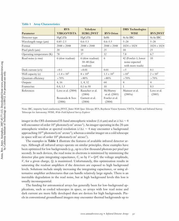
Table 1 Array Characteristics
ParameterRVS
VIRGO/VISTATeledyne
H2RG JWST RVS OrionDRS Technologies
WISE RVS JWSTDetector type HgCdTe HgCdTe InSb Si:As IBC Si:As IBCWavelength range (μm) 0.85–2.5 0.6–5.3 0.6–5.5 5–28 5–28Format 2048 × 2048 2048 × 2048 2048 × 2048 1024 × 1024 1024 × 1024Pixel pitch (μm) 20 18 25 18 25Operating temperature (K) 78 37 32 7.8 6.7Read noise (e rms) 6 (slow readout) 6 (slow readout)
30–40 (fastreadout)
6 42 (Fowler-1; lowernoise expectedwith more reads)
10
Dark current (e/s) <0.1 <0.01 0.01 <5 0.1Well capacity (e) >1.4 × 10⁵ 8 × 10⁴ 1.5 × 10⁵ >105 2 × 10⁵
Quantum efficiency >70% >80% >80% >70% >70%Outputs 4, 16 1, 4, 32 64 4 4Frames/sec 0.4, 1.5 0.1 to 30 10 1 0.3References Love et al. (2004) Rauscher et al.
(2004)McMurtryet al. (2003)
Mainzer et al.(2005a)
Love et al.(2005)
Bezawada & Ives(2006)
Garnett et al.(2004)
Fowler et al.(2004)
Note: IBC, impurity band conduction; JWST, James Webb Space Telescope; RVS, Raytheon Vision Systems; VISTA, Visible and Infrared SurveyTelescope for Astronomy; WISE, Wide-Field Infrared Survey Explorer.
imager in the OH-dominated H-band atmospheric window (1.6 μm) and at λ/�λ ∼ 4will encounter of order 104 photons/(s m2 arcsec2). An imager operating in the 20-μmatmospheric window at spectral resolution λ/�λ ∼ 4 may encounter a backgroundapproaching 1010 photons/(s m2 arcsec2), whereas a similar imager on a cold telescopein space will see of order 104 photons/(s m2 arcsec2).
The examples in Table 1 illustrate the features of available infrared detector ar-rays. Although all infrared arrays operate on similar principles, these examples havebeen optimized for low backgrounds (e.g., up to a few thousand photons per pixel persecond). In such devices, the read noise in electrons is minimized by minimizing thedetector plus gate integrating capacitance, C, so by V = Q/C the voltage amplitude,V, for a given charge, Q, is maximized. Unfortunately, this optimization results insaturating the readout amplifiers if the detectors are exposed to high backgroundlevels. Solutions include simply increasing the integrating capacitance, or using al-ternative amplifier architectures that can handle relatively large signals. There is aninevitable degradation in the read noise, but at high background levels this loss isusually inconsequential.
The funding for astronomical arrays has generally been for low-background ap-plications, such as cooled telescopes in space, so arrays with low read noise anddark current are more fully developed than are devices for high backgrounds. Pix-els in conventional groundbased imagers may encounter thermal backgrounds up to
www.annualreviews.org • Infrared Detector Arrays 91
Ann
u. R
ev. A
stro
. Ast
roph
ys. 2
007.
45:7
7-11
5. D
ownl
oade
d fr
om w
ww
.ann
ualr
evie
ws.
org
by C
alif
orni
a In
stitu
te o
f T
echn
olog
y on
11/
09/1
2. F
or p
erso
nal u
se o
nly.
ANRV320-AA45-03 ARI 24 July 2007 18:32
JWST: James Webb SpaceTelescope
109 photons/second. There are no modern arrays optimized for such backgroundsin the 3 μm to 5 μm region, and the largest available high-background Si:As IBCarrays are 256 × 256 or 240 × 320 pixels. However, there are plans to use the in-vestment in low-background 1024 × 1024 devices at DRS Technologies to leveragehigh-background arrays of the same format (Mainzer et al. 2005b; see also Love et al.2006).
5.1. Teledyne HgCdTe Arrays
Teledyne produces a variety of very high performance HgCdTe arrays. They include:(a) a line of devices initially used in the Near Infrared Camera and Multi-Object Spec-trometer (NICMOS) on the Hubble Space Telescope (e.g., Rieke et al. 1993) and thenin groundbased astronomy (including arrays far more advanced than the NICMOSones), mostly with a cutoff at 2.5 μm; (b) the devices derived from the ground-basedHAWAII-1 series (Hodapp et al. 1996) for the Wide Field Camera 3 on the HubbleSpace Telescope, with a cutoff wavelength of 1.72 μm (Robberto et al. 2004); and (c)arrays developed for the James Webb Space Telescope ( JWST), with cutoff wavelengthsof 2.5 μm and 5.3 μm (as in Table 1). The detectors for the current line of devices aremanufactured by MBE and have architecture similar to the diode shown in Figure 1.We describe in detail the 2048 × 2048 pixel HAWAII-2RG, but the other membersof the family are generally similar.
Referring to Figure 1 and Garnett et al. (2004a), growth of the detectors is carriedout on a CdZnTe substrate. This substrate material has been selected because it hasan excellent match to the HgCdTe crystal structure, which is important to minimizecrystal defects in the grown material. Defects in the detector crystal structure can actas traps for free electrons and thus degrade the performance. A previous generationof detectors from Rockwell used sapphire as the substrate, which provides a poorermatch.
First, the bulk HgCdTe is laid down, with the Hg and Cd fractions selected forthe appropriate band gap and cutoff wavelength. These first layers of material willeventually become the back side of the detector through which the photons enter. Thismaterial is doped with indium to make it n-type. The final stages of detector growthcap the device with a HgCdTe layer with higher band gap energy. This cap avoidshaving open bonds and crystal structure flaws at the detector front side. Because of thehigher band gap, it provides a potential barrier that reflects minority (photogenerated)carriers from the detector front side into the bulk material so they can diffuse into thejunction (a compositional gradient in the bulk material can also help drive minoritycarriers away from the front side). This control of minority carriers reduces cross talkand latent images and improves the quantum efficiency.
Once the layers have been grown, the pixels are defined by using arsenic to createp-type implants. The diode junction is formed at the interface between the implantedregion and the bulk n-type material. The detectors are completed by depositing aprotective layer of CdTe to passivate the device, and by depositing a metal contact oneach p-implant. Indium bumps are evaporated onto the metal contacts, in preparationfor hybridization. The CdZnTe can be removed after the detector array is complete,
92 Rieke
Ann
u. R
ev. A
stro
. Ast
roph
ys. 2
007.
45:7
7-11
5. D
ownl
oade
d fr
om w
ww
.ann
ualr
evie
ws.
org
by C
alif
orni
a In
stitu
te o
f T
echn
olog
y on
11/
09/1
2. F
or p
erso
nal u
se o
nly.
ANRV320-AA45-03 ARI 24 July 2007 18:32
because it blocks visible light photons and can also glow when struck by cosmicrays.
For these arrays, the readout is fabricated in a high-volume state-of-the-art com-mercial semiconductor foundry operated by United Microelectronics Corporation,using the standard foundry processes with 0.25-μm design rules. The outer four pixelsaround the periphery of the ROIC are used as reference pixels, so the light-sensitivearea is 2040 × 2040 pixels. The readout amplifiers are similar to those in Figure 3,but with additional MOSFETs to implement a sophisticated subarray readout mode.The ROIC contains a substantial amount of logic circuitry (MacDougal et al. 2006).This logic allows selection of 1-, 4-, or 32-output amplifiers, trading readout speedagainst power dissipation as the number of amplifiers increases. In addition, it ispossible to select a subarray section and read it out independently of the rest of thedevice, taking the signals to a dedicated output amplifier. One use of this capability isto allow centroiding on a stellar image to determine guiding corrections while takinglong exposures (e.g., Riopel, Teeple & Ward 2006). One can program different resetoptions, and select output gains between 1 and 16 times. The logic also allows foron-board identification and correction of single-event upsets from ionizing radiation.
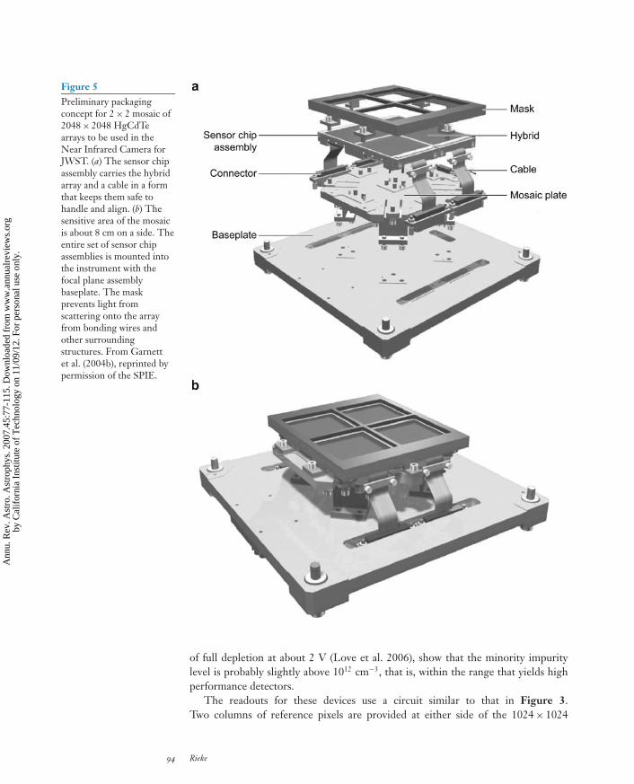
Each short wavelength optical train for the Near Infrared Camera on JWST willuse four of these arrays mounted in a mosaic as illustrated in Figure 5.
5.2. Raytheon Vision Systems Si:As IBC Arrays
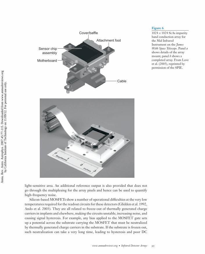
We now describe the 1024 × 1024 pixel Si:As IBC array being provided for the Mid-Infrared Instrument on JWST by RVS and shown in Figure 6. This device illustratesthe characteristics of other arrays using this detector type, which utilize similar de-tector processing and similar designs for their readouts.
These detectors are designed for the best broad-band response, i.e., highest pos-sible infrared absorption, because they are to be used down to 5 μm, where the Si:Asintrinsic absorption coefficient is relatively low. The detectors must also be designedto deplete the infrared-active layer fully. Otherwise, the quantum efficiency wouldbe reduced; furthermore, with simple readout amplifiers as in Figure 3, the outputwould be highly nonlinear as charge accumulates and changes the bias on the de-tector. The resulting design constraints are discussed by Love et al. (2004a) and canbe understood by refering to Figure 2 and the surrounding discussion. The goal isto produce the thickest possible infrared-active layer doped as heavily as possible,subject to the limitation that this layer should not become so conducting that thedetectors have a large dark current. This limit is reached at an arsenic concentrationof about 1018 cm−3. The layer thickness is set by the (unwanted) minority impurityconcentration and by the requirement that the bias voltage should not be so highthat it causes incipient avalanching of charge carriers and hence increased noise. Theminority impurity concentration upper limits are 1.44 × 1012 cm−3 for a 45-μm thicklayer, and 1.85 × 1012 cm−3 for a 35-μm thick layer (Love et al. 2004a). The detectorswere therefore designed for an arsenic doping level of 7 × 1017 cm−3 and a thickness of35 μm. The processing at Advanced Technology Materials, Inc., yielded devices veryclose to these targets. Measurements of the material characteristics, plus evidence
www.annualreviews.org • Infrared Detector Arrays 93
Ann
u. R
ev. A
stro
. Ast
roph
ys. 2
007.
45:7
7-11
5. D
ownl
oade
d fr
om w
ww
.ann
ualr
evie
ws.
org
by C
alif
orni
a In
stitu
te o
f T
echn
olog
y on
11/
09/1
2. F
or p
erso
nal u
se o
nly.
ANRV320-AA45-03 ARI 24 July 2007 18:32
Figure 5Preliminary packagingconcept for 2 × 2 mosaic of2048 × 2048 HgCdTearrays to be used in theNear Infrared Camera forJWST. (a) The sensor chipassembly carries the hybridarray and a cable in a formthat keeps them safe tohandle and align. (b) Thesensitive area of the mosaicis about 8 cm on a side. Theentire set of sensor chipassemblies is mounted intothe instrument with thefocal plane assemblybaseplate. The maskprevents light fromscattering onto the arrayfrom bonding wires andother surroundingstructures. From Garnettet al. (2004b), reprinted bypermission of the SPIE.
of full depletion at about 2 V (Love et al. 2006), show that the minority impuritylevel is probably slightly above 1012 cm−3, that is, within the range that yields highperformance detectors.
The readouts for these devices use a circuit similar to that in Figure 3.Two columns of reference pixels are provided at either side of the 1024 × 1024
94 Rieke
Ann
u. R
ev. A
stro
. Ast
roph
ys. 2
007.
45:7
7-11
5. D
ownl
oade
d fr
om w
ww
.ann
ualr
evie
ws.
org
by C
alif
orni
a In
stitu
te o
f T
echn
olog
y on
11/
09/1
2. F
or p
erso
nal u
se o
nly.
ANRV320-AA45-03 ARI 24 July 2007 18:32
Sensor chipassembly
Cover/baffle
Attachment foot
Motherboard
Cable
Figure 61024 × 1024 Si:As impurityband conduction array forthe Mid InfraredInstrument on the JamesWebb Space Telescope. Panel ashows details of the arraymount; panel b shows acompleted array. From Loveet al. (2005), reprinted bypermission of the SPIE.
light-sensitive area. An additional reference output is also provided that does notgo through the multiplexing for the array pixels and hence can be used to quantifyhigh-frequency noise.
Silicon-based MOSFETs show a number of operational difficulties at the very lowtemperatures required for the readout circuits for these detectors (Glidden et al. 1992,Ando et al. 2003). They are all related to freeze-out of thermally generated chargecarriers in implants and elsewhere, making the circuits unstable, increasing noise, andcausing signal hysteresis. For example, any bias applied to the MOSFET gate setsup a potential across the substrate carrying the MOSFET that must be neutralizedby thermally generated charge carriers in the substrate. If the substrate is frozen out,such neutralization can take a very long time, leading to hysteresis and poor DC
www.annualreviews.org • Infrared Detector Arrays 95
Ann
u. R
ev. A
stro
. Ast
roph
ys. 2
007.
45:7
7-11
5. D
ownl
oade
d fr
om w
ww
.ann
ualr
evie
ws.
org
by C
alif
orni
a In
stitu
te o
f T
echn
olog
y on
11/
09/1
2. F
or p
erso
nal u
se o
nly.
ANRV320-AA45-03 ARI 24 July 2007 18:32
VISTA: Visible andInfrared Survey Telescopefor Astronomy
stability. Many of these issues can be mitigated by growing the circuits on wafersthat are heavily—degenerately—doped except for a thin (3 μm to 6 μm) surface layerof high-purity silicon to carry the circuits and isolate them from the bulk material(Glidden et al. 1992). The heavy doping increases the concentration of free chargecarriers in the substrate so it is conducting even at very low temperature. As a result, itcan adjust quickly to changes in the MOSFET operating conditions. Such substratescan also conduct away the charge that would otherwise build up as a result of impactionization at the MOSFET drain electrode. In addition to this wafer design, a numberof modifications in the detailed circuit layout can also improve performance. Gliddenet al. (1992) discuss some possible approaches in detail. The resulting devices can beDC-stable and have low noise down to 1.5 K or below (Young et al. 1995).
RVS has established a process optimized for deep cryogenic operation at the Su-pertex foundry, where the readouts have been fabricated. The ROICs are built with2-μm design rules. Readouts with fine design rules (such as the 0.25 μm used forthe Teledyne arrays) can also function at these low temperatures without the deepcryogenic substrate design, in part because of the high current densities in their smallfeatures. However, their noise tends to be higher than has been achieved for the deepcryogenic readouts (see, e.g., Lum et al. 1993 for a comparison of the noise with earlyversions of these approaches).
5.3. Other Near- and Mid-Infrared Arrays
The first true infrared detector arrays to fly on a space astronomy mission were thetwo channels in the ISOCAM instrument on the ISO. The longer-wavelength deviceworked well and was responsible for a substantial part of the science return of themission. It was based on bulk Si:Ga photoconductors in a 32 × 32-pixel array readoutby a MOSFET amplifier array similar to those discussed above (Lucas et al. 1988;Mottier, Agnese & Lagage 1991).
There are a number of other arrays of interest to astronomers. RVS produces itsown 2024 × 2024-pixel 2.5 μm cutoff HgCdTe VIRGO arrays (Love et al. 2004b; seeTable 1). Like the Teledyne arrays, the detectors are grown on CdZnTe substrates,but using liquid phase epitaxy. If the substrate is removed and they are antireflectioncoated, they have very high quantum efficiency from the red to 2.5 μm. They also haveexcellent uniformity and can operate well up to temperatures of 70 K to 80 K. Thereadout design is modular in units of 512 × 1024 pixels, so it can support other arrayformats, and it can be used with HgCdTe detectors with other cutoff wavelengths.Sixteen of these arrays have been delivered in an open mosaic for the Wide-FieldVisible and Infrared Survey Telescope for Astronomy (VISTA) imager; the devicescan also be butted closely on three sides to make filled mosaics. In addition, RVSsupplies a high-performance InSb array, also listed in Table 1.
The Si:As IBC array from DRS Technologies, described in Table 1, benefits fromthe close interaction of the detector group with their supplier of Si:As detector wafers,Lawrence Semiconductor Research Laboratory, Inc. This team has developed themeans to control the minority impurity concentrations to levels significantly below1012 cm−3. Therefore, small bias voltages can fully deplete the infrared-active layer
96 Rieke
Ann
u. R
ev. A
stro
. Ast
roph
ys. 2
007.
45:7
7-11
5. D
ownl
oade
d fr
om w
ww
.ann
ualr
evie
ws.
org
by C
alif
orni
a In
stitu
te o
f T
echn
olog
y on
11/
09/1
2. F
or p
erso
nal u
se o
nly.
ANRV320-AA45-03 ARI 24 July 2007 18:32
WISE: Wide-Field InfraredSurvey Explorer
with minimum dark currents, allowing operation at relatively high temperatures. Thisattribute is important for use in the Wide-Field Infrared Survey Explorer (WISE) wherethe focal plane will be cooled in a solid hydrogen cryostat to 7.0 ± 0.5 K (Mainzeret al. 2005a).
In space, dislocation damage from cosmic ray hits within the blocking layer candegrade the dark current in Si:As IBC detectors (e.g., Heras et al. 2000). The smallrequired bias for the ultrahigh purity DRS detectors improves the tolerance to suchdamage. The readout for this array is manufactured in a standard commercial foundryusing fine design rules, rather than the optimized deep cryogenic architecture for theRVS array. The readout works well, and there is the potential that further optimizationof its operation can bring the noise down into the range of the deep cryogenic devices(e.g., as for the JWST Si:As IBC array in Table 1).
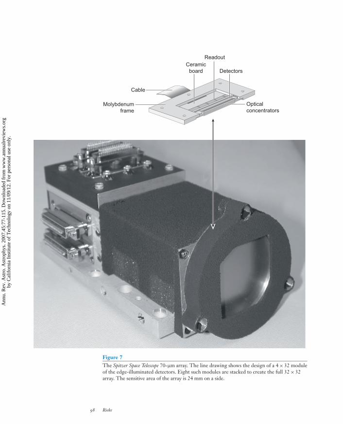
5.4. Far-Infrared Photoconductive Arrays
At wavelengths beyond 40 μm, there is no suitable silicon-based photoconductortechnology for high-performance arrays. Instead, IRAS, ISO, and Spitzer have allused bulk germanium photoconductors. The first two missions used individual sensorsoperated in parallel. However, for Spitzer a true 32 × 32-pixel array was developedfor the 70-μm band (Young et al. 1998). To allow for the long absorption path in thismaterial, the detectors are illuminated edge-wise with transverse contacts, and thereadouts are hidden behind them (see Figure 7). This construction style is sometimescalled Z-plane to indicate that the array has substantial size in the third dimension.The readouts use an ancestor of the RVS cryogenic process (discussed at the endof Section 5.2) to provide the necessary stability to maintain the small (45 mV) butsensitive bias settings required by these detectors. In addition, the amplifier designis modified from the simple integrator in Figure 3 to include electrical feedback tostabilize the detector bias during integrations.
The poor absorption of the Ge:Ga detector material requires that the detectorsin this array be huge—2 mm long. As a result, they have large cross sections forhits by ionizing particles, and in fact are hit on orbit every 10 s to 15 s. When apixel is hit, the electrical feedback on its readout amplifier quickly returns its bias tothe nominal value (within a fraction of a second). As a result, cross talk of the hit toneighboring pixels is minimized. In addition, it is possible to recover much of the datain an integration both before and after the hit; there is a transient on the integrationramp, but it quickly returns to normal.
Far-infrared photoconductor arrays suffer from the standard bulk photoconduc-tor photometric issues. In Spitzer, these problems have been addressed by flashing acalibrator to measure the response of all the pixels approximately every two minutes.The data pipeline interpolates between these calibrations to provide an instantaneousresponse map of the array. When measuring point sources, the pipeline removes acolumn-by-column offset determined by median averaging along the columns. Italso allows digital filtering in the time domain to suppress the slow response compo-nents. The final result is photometry that repeats to about 5% (Gordon et al. 2005,2007).
www.annualreviews.org • Infrared Detector Arrays 97
Ann
u. R
ev. A
stro
. Ast
roph
ys. 2
007.
45:7
7-11
5. D
ownl
oade
d fr
om w
ww
.ann
ualr
evie
ws.
org
by C
alif
orni
a In
stitu
te o
f T
echn
olog
y on
11/
09/1
2. F
or p
erso
nal u
se o
nly.
ANRV320-AA45-03 ARI 24 July 2007 18:32
Molybdenumframe
Cable
Ceramicboard Detectors
Readout
Optical concentrators
Figure 7The Spitzer Space Telescope 70-μm array. The line drawing shows the design of a 4 × 32 moduleof the edge-illuminated detectors. Eight such modules are stacked to create the full 32 × 32array. The sensitive area of the array is 24 mm on a side.
98 Rieke
Ann
u. R
ev. A
stro
. Ast
roph
ys. 2
007.
45:7
7-11
5. D
ownl
oade
d fr
om w
ww
.ann
ualr
evie
ws.
org
by C
alif
orni
a In
stitu
te o
f T
echn
olog
y on
11/
09/1
2. F
or p
erso
nal u
se o
nly.
ANRV320-AA45-03 ARI 24 July 2007 18:32
PACS: PhotodetectorArray Camera andSpectrometer
NEP: noise equivalentpower
Akari is currently observing with four small arrays of bulk germanium photo-conductors (30 to 60 pixels each), covering together the 50 μm to 180 μm spectralrange (Fujiwara et al. 2003, Shirahata et al. 2004). Two 16 × 25-pixel arrays of bulkgermanium photoconductors will also be flown in the Photodetector Array Cameraand Spectrometer (PACS) on Herschel (Poglitsch et al. 2003, Birkmann et al. 2004).Despite the photometric issues, these detectors have the advantages of rugged con-struction and of operation at relatively high temperature (about 1.5 K). However, adifferent detector type, bolometers, is capable of better performance so long as thedetectors can be cooled to sub-Kelvin temperatures.
6. BOLOMETER ARRAYS
6.1. Bolometer Principles of Operation
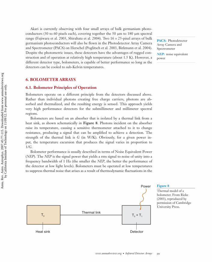
Bolometers operate on a different principle from the detectors discussed above.Rather than individual photons creating free charge carriers, photons are ab-sorbed and thermalized, and the resulting energy is sensed. This approach yieldsvery high performance detectors for the submillimeter and millimeter spectralregions.
Bolometers are based on an absorber that is isolated by a thermal link from aheat sink, as shown schematically in Figure 8. Photons incident on the absorberraise its temperature, causing a sensitive thermometer attached to it to changeresistance, producing a signal that can be amplified to achieve a detection. Thestrength of the thermal link is G (in W/K). Obviously, for a given power in-put, the temperature excursion that produces the signal varies in proportion to1/G.
Bolometer performance is usually described in terms of Noise Equivalent Power(NEP). The NEP is the signal power that yields a rms signal to noise of unity into afrequency bandwidth of 1 Hz (the smaller the NEP, the better the performance ofthe detector at low light levels). Bolometers must be operated at low temperaturesto suppress thermal noise that arises as a result of thermodynamic fluctuations in the
T0 + T1
Heat sink
Thermal linkT0
Detector
Power Figure 8Thermal model of abolometer. From Rieke(2003), reproduced bypermission of CambridgeUniversity Press.
www.annualreviews.org • Infrared Detector Arrays 99
Ann
u. R
ev. A
stro
. Ast
roph
ys. 2
007.
45:7
7-11
5. D
ownl
oade
d fr
om w
ww
.ann
ualr
evie
ws.
org
by C
alif
orni
a In
stitu
te o
f T
echn
olog
y on
11/
09/1
2. F
or p
erso
nal u
se o
nly.
ANRV320-AA45-03 ARI 24 July 2007 18:32
JFET: junction field effecttransistor
flow of energy across the thermal link:
NEPT = (4kT 2G )1/2
η, (5)
where k is Boltzmann’s constant, T is the temperature, and η is the quantum efficiency.Bolometers operating at sub-Kelvin temperatures can be designed so the thermalnoise is the ultimate limit, but bolometer noise may also have a significant contri-bution from Johnson noise. The corresponding component of the NEP is roughlyproportional to T2G, even more steeply dependent on temperature than NEPT . Alogical reaction to Equation 5 (and to our earlier statement that the signal-producingtemperature excursions grow inversely with G) would be that performance could beimproved without limit by reducing G. However, the thermal time constant of thebolometer is
τT = �
G, (6)
where � is the heat capacity. Even though the realized speed of the detector canbe increased through feedback from the bias circuit (discussed below), high perfor-mance with adequate time response demands low heat capacity. The specific heatsof bolometer materials—dielectrics, semiconductors, and metals—all decrease withdecreasing temperature. Bolometers are operated at very low temperature both toreduce thermal noise and to reduce the response time.
A bolometer operates best when the combination of heat dissipated in the ther-mometer plus the heat from the infrared background raises its temperature to about1.5 times that of its heat sink. For linear response, the power dissipated in the ther-mometer must exceed the infrared power. These constraints set optimum valuesto G and the operating temperature even when the time response is not an is-sue. Empirically, it is found that the achievable NEP scales approximately as T 2−2.5
(Rieke 2003). Achieving photon-noise-limited performance requires temperatures of∼0.3 K on the ground and ∼0.1 K when using cold optics in space.
6.2. Transistor Readout Bolometer Arrays
Very high performance bolometers have been built into small arrays for some time,but until recently these devices were based on parallel operation of single pixels (fora specific example, see Rownd et al. 2003, Nguyen et al. 2006). The obstacle to truearray-type construction was that the very small signals required use of junction fieldeffect transistor ( JFET) amplifiers that needed to operate above about 50 K, farabove the operating temperature of 0.3 K or below for the bolometers themselves. Itis difficult to implement the simple integration of detector and amplifier that is theheart of array construction with this temperature difference.
With the development of adequately low-noise readouts that can operate near thebolometer temperature, the first true high-performance bolometer arrays for the far-infrared and submillimeter spectral ranges are just becoming available. For example,the Herschel/PACS instrument uses a 2048-pixel array of bolometers (Billot et al.2006). The architecture of this array is vaguely similar to the direct hybrid arrays for
100 Rieke
Ann
u. R
ev. A
stro
. Ast
roph
ys. 2
007.
45:7
7-11
5. D
ownl
oade
d fr
om w
ww
.ann
ualr
evie
ws.
org
by C
alif
orni
a In
stitu
te o
f T
echn
olog
y on
11/
09/1
2. F
or p
erso
nal u
se o
nly.
ANRV320-AA45-03 ARI 24 July 2007 18:32
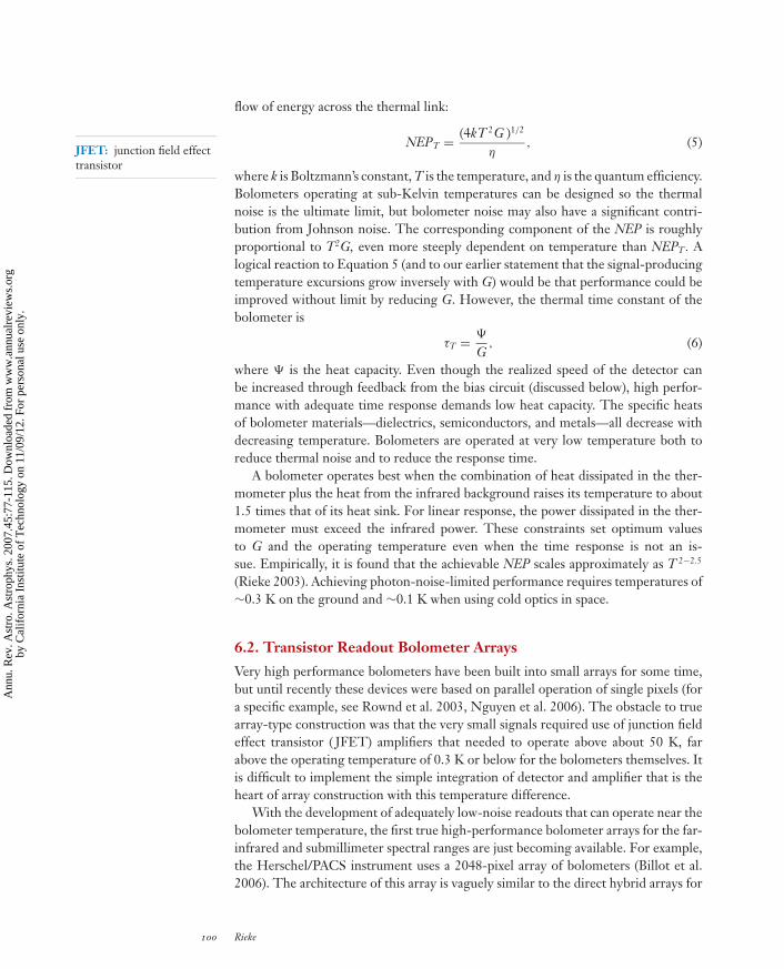
the near- and mid-infrared. One silicon wafer is patterned with bolometers, each inthe form of a silicon mesh, as shown in Figure 9. The delicate construction of thedetector depends on the ability to etch exquisitely complex miniature structures insilicon. The development of silicon micromachining has enabled substantial advancesin bolometer construction generally and is central to making large-scale arrays. In thisinstance, the silicon mechanical structure around the mesh region provides the heatsink; the mesh is isolated from it with thin and long silicon rods. Numerical model-ing allows optimization of the structure both for thermal properties and for efficientphoton absorption. The rods and mesh both need to be designed carefully to achieveappropriate response and time constant characteristics. The mesh is blackened witha thin layer of titanium nitride with sheet resistance matched to the impedance offree space (377 �/square section of film). This matching provides an efficiency of
Figure 9A single pixel in the Herschel/PACS bolometer array, pixel size about 750 μm, from P. Agnese(private communication).
www.annualreviews.org • Infrared Detector Arrays 101
Ann
u. R
ev. A
stro
. Ast
roph
ys. 2
007.
45:7
7-11
5. D
ownl
oade
d fr
om w
ww
.ann
ualr
evie
ws.
org
by C
alif
orni
a In
stitu
te o
f T
echn
olog
y on
11/
09/1
2. F
or p
erso
nal u
se o
nly.
ANRV320-AA45-03 ARI 24 July 2007 18:32
TES: transition edge sensor
SCUBA: SubmillimetreCommon-User BolometerArray
SQUID: superconductingquantum interference device
50% over a broad band in absorbing submillimeter- or millimeter-wave photons.Quarter-wave resonant structures can tune the absorption to higher values over lim-ited spectral bands. For each bolometer a silicon-based thermometer doped by ionimplantation to have appropriate temperature-sensitive resistance lies at the center ofthe mesh. Large resistance values are used so the fundamental noise is large enoughto utilize MOSFET readout amplifiers. A second silicon wafer is used to fabricate theMOSFET-based readouts, and the two are joined by indium bump bonding. Whenfar-infrared photons impinge on the array, they are absorbed by the grids and raisethe temperatures of the thermometers. The resulting resistance changes are sensedby the readouts, amplified, and conveyed to the external electronics. To minimizethermal noise and optimize the material properties, the bolometer array is operatedat 0.3 K. Further details are in Billot et al. (2006). Application of similar arrays onground-based telescopes is discussed by Talvard et al. (2006).
6.3. Transition Edge Sensor Bolometers with SuperconductingReadouts
Another approach is taken in transition edge sensor (TES) arrays such as the ones to beused in the submillimeter camera SCUBA (Submillimetre Common-User BolometerArray)-2. A short discussion of these arrays can be found in Walton et al. (2004), whileIrwin & Hilton (2005) and Clarke et al. (2006) provide thorough reviews of TES-based bolometers and readout electronics in general. The name of these devices isderived from their thermometers, which are based on thin superconducting films heldwithin their transition region, where they change from the superconducting to thenormal state over a temperature range of a few milliKelvin. In this region, the filmshave a stable but very steep dependence of resistance on temperature. The tempera-ture of this transition can be set to a convenient point by using a bilayer film consistingof a layer of normal material and a layer of superconductor. The Cooper pairs from thesuperconductor can diffuse into the normal metal and make it weakly superconduct-ing, a process called the proximity effect. As a result, the transition temperature is low-ered relative to that for the pure superconducting film. Adjusting the film thicknesseschanges the extent of the effect and adjusts the transition temperature to a convenientvalue (e.g., one appropriate for a specific type of low-temperature refrigerator).
However, the resistance of a TES is low, so it can deliver significant power onlyto low-input impedance amplifiers, which rules out JFETs and MOSFETs. Instead,the signals are fed into superconducting quantum interference devices (SQUIDs; seeFigure 10). SQUIDs are the basis for a growing family of electronic devices thatoperate by superconductivity (e.g., Clarke & Braginski 2006).
Because of the steep temperature dependence of their resistance, TESs are moststable when biased with a constant voltage. The SCUBA-2 devices, as with all TESbolometers, are operated in this mode (see Figure 10 for a typical bias circuit).In this state, when their temperature rises due to power from absorbed photons,their resistance rises, the bias current drops, and the electrical power dissipation inthem decreases, partially canceling the effects of the absorbed power and limiting thenet thermal excursion. This behavior is called electrothermal feedback. The steep
102 Rieke
Ann
u. R
ev. A
stro
. Ast
roph
ys. 2
007.
45:7
7-11
5. D
ownl
oade
d fr
om w
ww
.ann
ualr
evie
ws.
org
by C
alif
orni
a In
stitu
te o
f T
echn
olog
y on
11/
09/1
2. F
or p
erso
nal u
se o
nly.
ANRV320-AA45-03 ARI 24 July 2007 18:32
temperature dependence of the resistance of a TES makes the effect very strong.This feedback expedites operating arrays with TESs because minor variations in thetransition temperature can be overcome by the tendency of the feedback to forceeach device to a suitable operating point. Electrothermal feedback can also make thebolometers operate tens or even hundreds of times faster than implied by Equation 6.In fact, if the TES is too fast, the bolometer/SQUID circuit can be unstable andmeasures must be taken to slow the response.
TES bolometer arrays use SQUIDs for the same readout functions that we havediscussed for photodiode and IBC detector arrays. The operation of a simple SQUIDtime-domain multiplexer is illustrated in Figure 10 (Benford et al. 2000). The biasesacross the SQUIDs are controlled by the address lines. Each SQUID can be switchedfrom an operational state to a superconducting one if it is biased to carry about 100 μA.The address lines are set so all the SQUIDs in series are superconducting except one,and then only that one contributes to the output voltage. By a suitable series of biassettings, each SQUID amplifier can be read out in turn.
From our perspective, a major advance in these devices is that the superconduct-ing readouts operate with very low power dissipation and at the ultralow tempera-ture required for the bolometers. Therefore, integration of detectors and readoutsis simplified and the architecture can potentially be scaled to very large arrays. EachSCUBA-2 array is made of four subarrays, each with 1280 transition-edge sensors.The design is illustrated in Figure 11. The detector elements are separated fromtheir heat sinks by a deep etched trench that is bridged by only a thin silicon nitridemembrane. The absorbing surface is blackened by implanting it with phosphorus tomatch the impedance of free space. The dimensions of the array pixels are adjustedthrough numerical modeling to form a resonant cavity at the wavelength of operation,to enhance the absorption efficiency. The superconducting electronics that read outthe bolometers are fabricated on separate wafers. The two components are assem-bled into an array using indium bump bonding. Further details are in Griffin (2000),Walton et al. (2004), and Woodcraft et al. (2006).
In addition to the arrays for SCUBA-2, various forms of TES-based bolometerswith SQUID readouts are under active development in a number of laboratories (e.g.,Benford et al. 2006, May et al. 2006). For example, in the millimeter-wave range thepixel-based array geometry in Figures 10 and 11 can be replaced with tiny antennaedefined by photolithography (Myers et al. 2002). The operating spectral range ofantenna-coupled bolometers lies between the infrared and radio and they make useof a mixture of technologies from both spectral regimes. The antenna feeds respondto a single polarization, an advantage if the detectors are planned for a polarimeter.Antennae can be arranged in a single focal plane to measure several polarizationangles simultaneously. Microstrip transmission lines can bring the antenna signalsoutside the sensitive area of the array (a microstrip consists of a miniature circuit traceon an insulator and over a ground plane that can be designed to have some of thecharacteristics of a waveguide). There, the signals can be sent to a bank of microstripfilters that separate them into multiple spectral bands. Microstrip transmission linescarrying the signals are then terminated with normally conducting metal resistorsand TESs sense the temperatures of the resistors as a measure of the power received
www.annualreviews.org • Infrared Detector Arrays 103
Ann
u. R
ev. A
stro
. Ast
roph
ys. 2
007.
45:7
7-11
5. D
ownl
oade
d fr
om w
ww
.ann
ualr
evie
ws.
org
by C
alif
orni
a In
stitu
te o
f T
echn
olog
y on
11/
09/1
2. F
or p
erso
nal u
se o
nly.
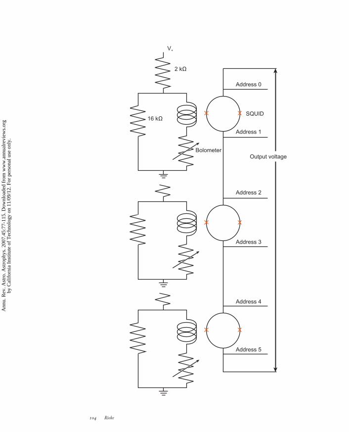
ANRV320-AA45-03 ARI 24 July 2007 18:32
Address 0
Address 1
Address 2
Address 3
Address 4
Address 5
Output voltage
SQUID
Bolometer
2 kΩ
16 kΩ
V+
104 Rieke
Ann
u. R
ev. A
stro
. Ast
roph
ys. 2
007.
45:7
7-11
5. D
ownl
oade
d fr
om w
ww
.ann
ualr
evie
ws.
org
by C
alif
orni
a In
stitu
te o
f T
echn
olog
y on
11/
09/1
2. F
or p
erso
nal u
se o
nly.
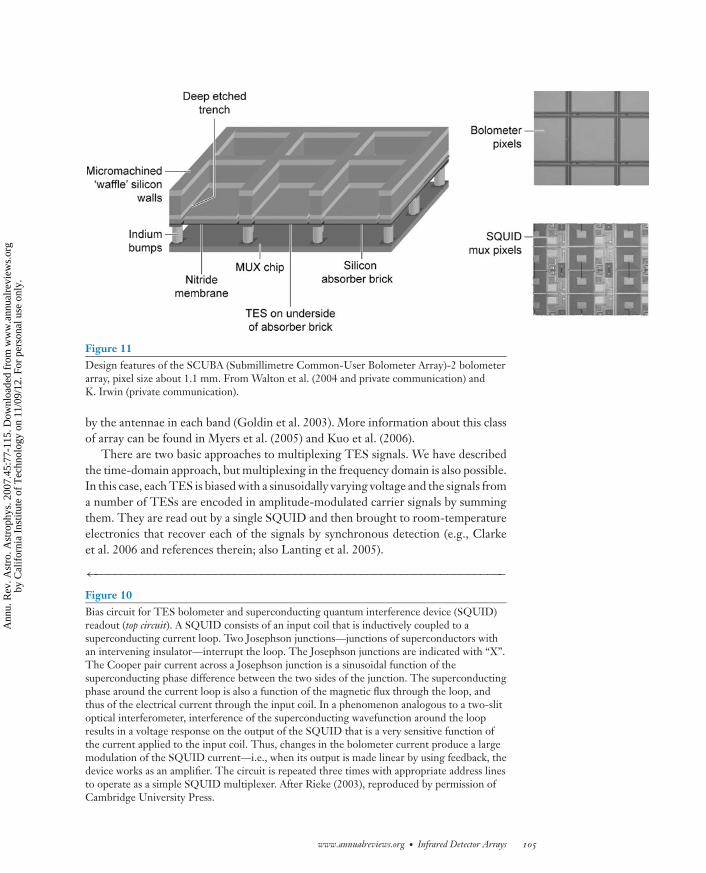
ANRV320-AA45-03 ARI 24 July 2007 18:32
Figure 11Design features of the SCUBA (Submillimetre Common-User Bolometer Array)-2 bolometerarray, pixel size about 1.1 mm. From Walton et al. (2004 and private communication) andK. Irwin (private communication).
by the antennae in each band (Goldin et al. 2003). More information about this classof array can be found in Myers et al. (2005) and Kuo et al. (2006).
There are two basic approaches to multiplexing TES signals. We have describedthe time-domain approach, but multiplexing in the frequency domain is also possible.In this case, each TES is biased with a sinusoidally varying voltage and the signals froma number of TESs are encoded in amplitude-modulated carrier signals by summingthem. They are read out by a single SQUID and then brought to room-temperatureelectronics that recover each of the signals by synchronous detection (e.g., Clarkeet al. 2006 and references therein; also Lanting et al. 2005).
←−−−−−−−−−−−−−−−−−−−−−−−−−−−−−−−−−−−−−−−−−−−−−−−−−−−−−−−−−−−−−−Figure 10Bias circuit for TES bolometer and superconducting quantum interference device (SQUID)readout (top circuit). A SQUID consists of an input coil that is inductively coupled to asuperconducting current loop. Two Josephson junctions—junctions of superconductors withan intervening insulator—interrupt the loop. The Josephson junctions are indicated with “X”.The Cooper pair current across a Josephson junction is a sinusoidal function of thesuperconducting phase difference between the two sides of the junction. The superconductingphase around the current loop is also a function of the magnetic flux through the loop, andthus of the electrical current through the input coil. In a phenomenon analogous to a two-slitoptical interferometer, interference of the superconducting wavefunction around the loopresults in a voltage response on the output of the SQUID that is a very sensitive function ofthe current applied to the input coil. Thus, changes in the bolometer current produce a largemodulation of the SQUID current—i.e., when its output is made linear by using feedback, thedevice works as an amplifier. The circuit is repeated three times with appropriate address linesto operate as a simple SQUID multiplexer. After Rieke (2003), reproduced by permission ofCambridge University Press.
www.annualreviews.org • Infrared Detector Arrays 105
Ann
u. R
ev. A
stro
. Ast
roph
ys. 2
007.
45:7
7-11
5. D
ownl
oade
d fr
om w
ww
.ann
ualr
evie
ws.
org
by C
alif
orni
a In
stitu
te o
f T
echn
olog
y on
11/
09/1
2. F
or p
erso
nal u
se o
nly.
ANRV320-AA45-03 ARI 24 July 2007 18:32
7. APPLICATION OF INFRARED ARRAYS
7.1. Basic Performance
“Sufficiently advanced technology is indistinguishable from magic” (Clarke 1962). Toanyone who has worked in the single-pixel era of infrared astronomy, modern detectorarrays carry an aura of magic. As with CCDs in the optical, we are approaching per-fection in the near-infrared. That is, we can use very large format arrays of detectors,each of which has nearly 100% quantum efficiency and sufficiently low read noiseand dark current that they do not degrade the photon-limited performance in mostcircumstances. These arrays have sufficient flexibility for most astronomical applica-tions: their wells can accommodate the backgrounds, and they can operate at highspeed by reading out subarrays. We are also approaching perfection with regard toarrays between 3 μm and 28 μm for space astronomy missions. The high backgroundsencountered on the ground require changes in array architecture that have not beenimplemented as broadly, but there are no fundamental technical obstacles to reachnear-perfection for these applications also. Beyond 28 μm, array technology is ad-vancing rapidly and, as a result, the possibilities for new astronomical breakthroughsare growing.
As optical astronomers have demonstrated, nearly perfect detector arrays are notthe end of the road. Instead, it becomes sensible to invest in ambitious instrumentationknowing that a new array technology is unlikely to make the investment obsolete in afew years. For example, infrared arrays of the current generation have been designedto make two- or even three-sided butting possible. Hence, they can fill large imagingfields of view efficiently or can provide large formats for spectrometers, developmentsthat are being pursued at a number of observatories (e.g., Figure 5).
7.2. Data Processing
In general, it becomes more difficult to achieve cosmetically uniform images froman array as the wavelength of operation is increased. As the absorbed photon en-ergy decreases, the relative importance of small nonuniformities in the array de-tectors grows. Therefore, to appreciate the quality of the data provided with in-frared arrays requires a series of careful processing steps. In comparison, a CCD canproduce a cosmetically acceptable image without detailed processing, although sci-entific use of that image requires processing similar to that required with infraredarrays.
In the section below, we describe artifacts that may appear in infrared images evenafter a standard set of processing steps. Here we assume a reasonably ideal array subjectonly to nonuniformities that appear as noise but remain reasonably independent ofconditions and that can be removed from the data in a standard series of processingsteps. There are the following sources of such nonuniformities:
1. Zero variations are caused by electronic or temperature drifts that generallydepend on the elapsed time and the temperature stability of the array and itsreadout electronics.
106 Rieke
Ann
u. R
ev. A
stro
. Ast
roph
ys. 2
007.
45:7
7-11
5. D
ownl
oade
d fr
om w
ww
.ann
ualr
evie
ws.
org
by C
alif
orni
a In
stitu
te o
f T
echn
olog
y on
11/
09/1
2. F
or p
erso
nal u
se o
nly.
ANRV320-AA45-03 ARI 24 July 2007 18:32
2. Offset or bias variations have amplitudes that are fixed, independent of signallevel, integration time, and elapsed time. They can result from the layout ofthe ROICs, or from electronic signals that are coupled into the ROIC in anonvariable way.
3. Dark currents depend on integration time but not on signal level. Signals dueto photon leaks can sometimes be treated in the data analysis identically to truedark currents, if they also depend only on integration time.
4. Pixel response variations depend on both signal level and integration time,normally as the product.
Four types of calibration data are required to remove these sources of noise. Zerovariations can be mitigated by appropriate use of reference pixel outputs. A set ofvery short exposures with the detector in the dark can be averaged to provide ahigh signal-to-noise image of the offset variations, which can be subtracted from thescience image. Dark currents can in principle be removed by taking long exposuresin the dark, scaling the signals to the actual exposure time, and subtracting. However,this approach requires ideal behavior of the entire system, so it is safer to take the darkframes with the identical exposure as the science image. In general, the dark frameswill embed the offset variations, so removing the latter specifically may be unnecessaryif dark frames are used (however, in some cases the dark current is negligible, and thenit may be more efficient to ignore it and just concentrate on removing the offsets).Response variations are removed by dividing by an image formed by averaging manyexposures on a uniform background.
All of these processing steps work best if the operating conditions of the array arekept as constant as possible throughout acquisition of the science data and calibrationimages. In this regard, we again emphasize the desirability of maintaining a constantreadout cadence on the arrays. Where the infrared backgrounds are substantial com-pared with the signal (nearly always the case from the ground and often in space),high quality flat field frames must generally be obtained on the sky under identicalconditions as those for the data frames. This goal can be accomplished for imagesby dithering the telescope pointing to obtain many exposures and then using imageprocessing to remove the source signals to produce the flat field frames. Strategiesfor spectra are more complex and depend on the nature of the spectrometer. In anycase, the flat field frames must have zeros, offsets, and dark currents removed as inthe data frames, and then they can be divided into the data frames to yield reducedimages.
7.3. Artifacts
As good as modern infrared arrays are, they still have a few quirks that are not neces-sarily removed by the processing steps described above. We try to give a reasonablycomplete catalog of them to help users identify possible problems in array data. Weconcentrate this discussion on near- and mid-infrared arrays rather than bolometersbecause of the far greater observing experience with the former devices (bolometerarrays are only in the first stages of use for astronomical observations).
www.annualreviews.org • Infrared Detector Arrays 107
Ann
u. R
ev. A
stro
. Ast
roph
ys. 2
007.
45:7
7-11
5. D
ownl
oade
d fr
om w
ww
.ann
ualr
evie
ws.
org
by C
alif
orni
a In
stitu
te o
f T
echn
olog
y on
11/
09/1
2. F
or p
erso
nal u
se o
nly.
ANRV320-AA45-03 ARI 24 July 2007 18:32
7.3.1. Electronic. In general, science-grade detector arrays have more than 99%operative pixels. The exceptional pixels are either dead, producing no signals, or hot,with high dark currents. The pixels also have a distribution of read noises, approxi-mately Gaussian in shape but with a tail extending to high values.
Most infrared arrays exhibit a small degree of nonlinearity. Even with proper biassettings, there is a slow reduction in response as signals increase. A typical readoutamplifier reduces the detector bias as charge is collected, which directly reducesthe response. Reduced bias can also change the detector characteristics to producesimilar effects. For example, as the bias on a photodiode is reduced, the width of itsdepletion region decreases and its capacitance increases, thus reducing the gain of thedetector/amplifier combination. Under typical operating conditions, these effects aregenerally no more than a few percent. If the bias is set too low, the effects on linearitycan be much larger, as we have already discussed for IBC detectors.
Bright sources can produce another set of effects, such as duplicate images, pulldown of the response along rows of detectors in the array, and bleeding of the signalinto additional output channels. These issues can be mitigated by careful design ofthe array control and bias-supply electronic circuits.
Offsets of the signal are another category of electronic problems. A fixed patternof offsets can arise from the layout of the ROIC. When arrays are reset, their outputsmay end up significantly displaced from zero signal and with large-scale patterns overthe array reflecting a gradient in the offset, a class of effect sometimes called a resetanomaly. In the case of the IBC arrays used in the Spitzer Infrared Spectrographand Multiband Imaging Photometer instruments, there is droop, where the outputincludes a signal proportional to the total signal incident on the array as well as theusual component proportional to the signal on the pixel. There can also be fixedlevels of electrical cross talk in the signal. Most of these effects are relatively benign,in that they do not cause noise in proportion to the signals they produce. Therefore,appropriate data processing strategies can remove them almost completely, althoughthey do reduce the dynamic range of the device. However, such effects can vary ifthe operating cadence of the array is changed, so a constant cadence is helpful inremoving them thoroughly from the data.
At the very demanding conditions for long integrations at low background, otherforms of subtle electronic misbehavior can manifest themselves. One such phe-nomenon is popcorn noise, a name derived because similar noise in an audio systemcan produce a sound reminiscent of popcorn popping (other names are burst noiseand telegraph noise). This behavior has been seen in prototype detectors for thenear-infrared JWST instruments (Rauscher et al. 2004) and other devices using thesame foundry process for the readouts. It takes the form of a rapid—apparently nearlyinstantaneous—transition between output levels, and can come in a broad variety ofjump sizes and patterns (Bacon et al. 2005). It is hypothesized that the underlyingcause is charge trapping in areas of the multiplexer that are particularly sensitive, butthe details of the noise mechanism are not well understood (Bacon et al. 2005 giveadditional references regarding the underlying mechanism). Popcorn noise can resultin a substantial degradation of the read noise. Its effects can be reduced by handlingthe array data in a way that allows rejection of the contaminated integrations (e.g., by
108 Rieke
Ann
u. R
ev. A
stro
. Ast
roph
ys. 2
007.
45:7
7-11
5. D
ownl
oade
d fr
om w
ww
.ann
ualr
evie
ws.
org
by C
alif
orni
a In
stitu
te o
f T
echn
olog
y on
11/
09/1
2. F
or p
erso
nal u
se o
nly.
ANRV320-AA45-03 ARI 24 July 2007 18:32
obtaining multiple samples along the integration ramp and rejecting segments withanomalous slopes).
Virtually all infrared arrays show latent images. For high-performance HgCdTedetectors, they can be as small as 0.03% of the original signal and decay in a fewminutes (e.g., Garnett et al. 2004b). For InSb, Si:As IBCs, and other array types, theycan start at up to 1% of the original signal in the first readout after a source has beenremoved from a pixel, and also decay in a few minutes. In some cases, when exposedto very strong inputs, there is a second class of latent image that requires many hoursto disappear unless mitigation steps are taken. Such steps can include raising thetemperature of the array sufficiently to thermalize it (termed annealing) or increasingits bias voltage to run a large current through it (bias boost). Latent images of thefirst kind can be readily identified in a series of images but those of the second kindare more difficult to remove because they tend to propagate into calibration framesused for flat fielding and other operations during the processing of the images.
The free charge carriers produced in an infrared detector upon exposure to ion-izing radiation are, of course, phenomenally well detected as spikes of conductivity.Ionizing radiation can produce a number of other effects. In bulk photoconductors,these effects can dominate the calibration uncertainties, but some of them can alsoexist at very low levels in other detector types. For example, some of the free chargecarriers can be captured by the minority impurities in the semiconductor, changingthe electric properties of the detector. As a result, at very low background operation,there can be a persistent boost in the detector responsivity but also in its noise. Athigh backgrounds, the recovery time is relatively short and these effects may notbe apparent. However, for good performance at low backgrounds, it may be nec-essary to remove them periodically by warming the detector (annealing) or otherstrategies. Fortunately, in detector types where the electrical and optical functionsare separated and where the infrared-active regions can therefore have relatively highconductivity—e.g., photodiodes or IBC devices—the susceptibility to these long-termionizing radiation effects is greatly reduced.
7.3.2. Optical. Because infrared arrays are constructed as thin parallel layers of semi-conductor with reflective contacts, they can have strong Fabry-Perot-type fringing atwavelengths where the photon absorption is not complete. This behavior can makeaccurate calibration of spectra challenging. Also, their pixels behave as isolated detec-tors and there can be reduced response in the gaps between them. The pixels may alsohave a low level of nonuniform response over their faces. In optical systems wherethe image is not well-sampled by the pixels, the resulting fixed grid of low responseregions and the dependence of the output on the exact placement of the source onthe pixels can make accurate calibration difficult.
Early infrared array readout multiplexers emitted light when their amplifiers dis-sipated significant levels of power. The array detectors could intercept the resultingmux glow to produce a signal. Although these signals were fixed in strength and dis-tribution over the array for a given readout pattern, and hence disappeared well in flatfield image processing, they did contribute noise. Such glow is an inherent propertyof silicon-based integrated circuits, but it is well controlled in modern arrays. It can
www.annualreviews.org • Infrared Detector Arrays 109
Ann
u. R
ev. A
stro
. Ast
roph
ys. 2
007.
45:7
7-11
5. D
ownl
oade
d fr
om w
ww
.ann
ualr
evie
ws.
org
by C
alif
orni
a In
stitu
te o
f T
echn
olog
y on
11/
09/1
2. F
or p
erso
nal u
se o
nly.
ANRV320-AA45-03 ARI 24 July 2007 18:32
be further reduced by applying power to the array ROIC only when the signals fromit are being read out. Glow is at sufficiently low levels in the current generation ofarrays that it is not a serious limitation so long as appropriate operational measuresare taken to minimize it.
Spurious light signals can also result from luminescence when energetic, ionizingparticles excite the materials in an array. Such glow can have time variability thatmakes it difficult to remove from the images. In addition, light can scatter fromexposed bonding wires onto the array from bright sources imaged off it, producinga complex pattern of signal that is virtually impossible to remove completely. It isalso sometimes possible for light to enter the detectors at the edge of an array fromthe side. Both of these issues can be removed by adding a light shield around theedge of the sensitive area. At wavelengths where the array absorption is low, light canalso pass through the detectors into the space between them and the readout. Thereit becomes trapped and undergoes multiple scatterings before it is absorbed. If thefinal absorption occurs in pixels of the array, the result is a very extended halo of alow level of response around an image. Although these halos are handled well in theusual methods for obtaining photometry of point sources, they make calibration ofextended source images complex.
8. SUMMARY
Very high performance near- and mid-infrared arrays have become available for as-tronomy over the past 20 years through a combination of (a) military investments toprove the hybrid array concept and to establish the infrastructure for manufacturingsuch devices, (b) sophisticated semiconductor detector architectures and the meansto fabricate them with good control over material properties, and (c) advanced inte-grated circuits on silicon. From 1 μm to 5 μm, the arrays use photodiodes in InSbor HgCdTe, whereas detectors operating from 5 μm to 40 μm are based on extrinsicphotoconductivity in silicon. It has been possible to apply some of these advances tothe first far-infrared arrays using doped germanium. Similar dramatic progress is oc-curring in the submillimeter- and millimeter-wave with superconducting bolometersenabled by (a) silicon micromachining to manufacture complex thermally isolateddetectors, (b) superconducting electronics for readout electronics that can operate atthe same ultralow temperatures as the detectors, (c) numerical modeling to optimizeabsorption efficiencies, and (d) refrigerators that maintain the devices at the 0.1 K to0.3 K temperatures required to suppress thermal noise and to provide the necessarymaterial properties.
At one level, the advances associated with these infrared detector arrays are summa-rized in Figure 12. The original discovery map of the Galactic Center (Figure 12a)was painstakingly put together from a few scans using a single detector on a 5-mtelescope, and required a number of nights. It is now easy to surpass the informationcontent of this map in a few seconds with a 1.3-m telescope (Figure 12b, 2MASSsurvey; the field shown is approximately the 2MASS array field of view, so the nomi-nal integration time is 8 s). Figure 12c was taken with a telescope of similar size (the6.5-m Magellan Telescope) as was used for the discovery map and in less time, but
110 Rieke
Ann
u. R
ev. A
stro
. Ast
roph
ys. 2
007.
45:7
7-11
5. D
ownl
oade
d fr
om w
ww
.ann
ualr
evie
ws.
org
by C
alif
orni
a In
stitu
te o
f T
echn
olog
y on
11/
09/1
2. F
or p
erso
nal u
se o
nly.
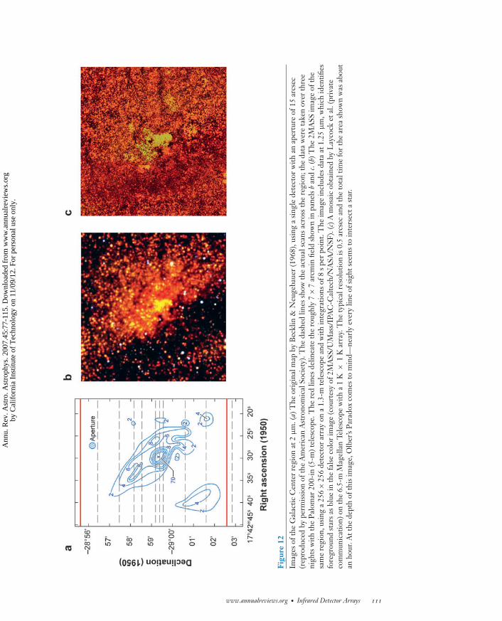
ANRV320-AA45-03 ARI 24 July 2007 18:32
Figu
re12
Imag
esof
the
Gal
actic
Cen
ter
regi
onat
2μ
m.(
a)T
heor
igin
alm
apby
Bec
klin
&N
euge
baue
r(1
968)
,usi
nga
sing
lede
tect
orw
ithan
aper
ture
of15
arcs
ec(r
epro
duce
dby
perm
issi
onof
the
Am
eric
anA
stro
nom
ical
Soci
ety)
.The
dash
edlin
essh
owth
eac
tual
scan
sac
ross
the
regi
on;t
heda
taw
ere
take
nov
erth
ree
nigh
tsw
ithth
eP
alom
ar20
0-in
(5-m
)tel
esco
pe.T
here
dlin
esde
linea
teth
ero
ughl
y7
×7
arcm
infie
ldsh
own
inpa
nels
ban
dc.
(b)T
he2M
ASS
imag
eof
the
sam
ere
gion
,usi
nga
256
×25
6de
tect
orar
ray
ona
1.3-
mte
lesc
ope
and
with
inte
grat
ions
of8
sper
poin
t.T
heim
age
incl
udes
data
at1.
25μ
m,w
hich
iden
tifies
fore
grou
ndst
ars
asbl
uein
the
fals
eco
lor
imag
e(c
ourt
esy
of2M
ASS
/UM
ass/
IPA
C-C
alte
ch/N
ASA
/NSF
).(c
)Am
osai
cob
tain
edby
Lay
cock
etal
.(pr
ivat
eco
mm
unic
atio
n)on
the
6.5-
mM
agel
lan
Tele
scop
ew
itha
1K
×1
Kar
ray.
The
typi
calr
esol
utio
nis
0.5
arcs
ecan
dth
eto
talt
ime
for
the
area
show
nw
asab
out
anho
ur.A
tthe
dept
hof
this
imag
e,O
lber
’sP
arad
oxco
mes
tom
ind—
near
lyev
ery
line
ofsi
ghts
eem
sto
inte
rsec
tast
ar.
www.annualreviews.org • Infrared Detector Arrays 111
Ann
u. R
ev. A
stro
. Ast
roph
ys. 2
007.
45:7
7-11
5. D
ownl
oade
d fr
om w
ww
.ann
ualr
evie
ws.
org
by C
alif
orni
a In
stitu
te o
f T
echn
olog
y on
11/
09/1
2. F
or p
erso
nal u
se o
nly.
ANRV320-AA45-03 ARI 24 July 2007 18:32
with a 1024 × 1024 array. The gain in resolution is about a factor of 30 and in depthby more than three orders of magnitude (for a point source).
Figure 12 illustrates the spectacular advances using detector arrays from theground, particularly in the near-infrared. At longer wavelengths, arrays have alsobrought great advances, but their ultimate performance is severely limited by theblinding thermal radiation of the telescope and atmosphere; also, much of the far-infrared is blocked by telluric atmospheric absorption. Modern mid- and far-infraredarrays can reach their full potential only when used on cold telescopes in space. Theastronomical capability quantified in Equation 1 can be extended to include the tele-scope by allowing for its effects on the system sensitivity. The gain in capability forJWST over Spitzer is about a factor of 104 throughout the mid-infrared. Similarly,an array similar to that being built for SCUBA-2 on a space-borne 10-m telescope[e.g., the Single Aperture Far Infrared Telescope (SAFIR)] would be capable of anadvance in capability by a factor of 104 to 105. These gains are of the same order asthe advances from one version of the Galactic Center image to the next in Figure 12.
ACKNOWLEDGMENTS
This work has benefited from comments and other assistance from James Beletic,James Garnett, Karl Gordon, Alan Hoffman, Henry Hogue, Kent Irwin, CraigMcCreight, Marcia Rieke, Paul Smith, Kate Su, Kadri Vural, Erick Young, and es-pecially Peter Love and Paul Richards. I also thank Patrick Agnese, Erick Becklin,James Garnett, Kent Irwin, Simon Laycock, Peter Love, Gerry Neugebauer, AnthonyWalton, the Cambridge and Arizona University Presses, the SPIE, and the AmericanAstronomical Society for permission to use figures. The work was partially sup-ported by contract 1255094 from Caltech/JPL and by contract NAG5-12318 fromNASA/Goddard, both to the University of Arizona.
LITERATURE CITED
Amico P, ed. 2004. Scientific Detectors for Astronomy: The Beginning of a New Era.Dordrecht: Kluwer Acad.
Ando KJ, Hoffman AW, Love PJ, Toth A, Anderson C, et al. 2003. Proc. SPIE5074:648–57
Arens JF, Lamb GM, Peck MC, Moseley H, Hoffmann WF, et al. 1984. Astrophys.J. 279:685–93
Bacon CM, McMurtry CW, Pipher JL, Forrest WJ, Garnett JD, et al. 2004. Proc.SPIE 5167:313–19
Bacon CM, McMurtry CW, Pipher JL, Forrest WJ, Garnett JD. 2005. Proc. SPIE5902:118–29
Bahcall JN, Beichman CA, Canizares C, Cronin J, Heeschen D, et al. 1991. TheDecade of Discovery in Astronomy and Astrophysics. Washington, DC: Natl. Acad.Press
Bandaru J, Beeman JW, Haller EE. 2002. Proc. SPIE 4486:193–99Becklin EE, Neugebauer G. 1968. Astrophys. J. 151:145–61
112 Rieke
Ann
u. R
ev. A
stro
. Ast
roph
ys. 2
007.
45:7
7-11
5. D
ownl
oade
d fr
om w
ww
.ann
ualr
evie
ws.
org
by C
alif
orni
a In
stitu
te o
f T
echn
olog
y on
11/
09/1
2. F
or p
erso
nal u
se o
nly.
ANRV320-AA45-03 ARI 24 July 2007 18:32
Beletic JE, Beletic JW, Amico P, eds. 2006. Scientific Detectors for Astronomy 2005.Netherlands: Springer-Verlag
Benford DJ, Allen CA, Chervenak JA, Grossman EN, Irwin KD, et al. 2000. ASPConf. Ser. 217:134–39
Benford DJ, Steguhn JG, Ames TJ, Allen CA, Chervenak JA, et al. 2006. Proc. SPIE6275:62751C, 12 pp.
Bezawada N, Ives D. 2006. See Beletic et al. 2006, pp. 499–506Billot N, Agnese P, Augueres JL, Beguin A, Bouere A, et al. 2006. Proc. SPIE
6265:62650D, 12 pp.Birkmann SM, Eberle K, Grozinger U, Lemke D, Schreiber J, et al. 2004. Proc. SPIE
5487:437–47Clarke AC. 1962. Profiles of the Future. New York: Harper & RowClarke J, Braginski AI, eds. 2006. The SQUID Handbook. Vol. II: Applications.
Weinheim, Ger.: Wiley-VCHClarke J, Lee AT, Muck M, Richards PL. 2006. See Clarke & Braginski 2006,
pp. 1–80Forrest WJ, Moneti A, Woodward CE, Pipher JL, Hoffman AW. 1985. PASP 97:183–
98Fowler AM, Merrill KM, Ball W, Henden A, Vrba F, McCreight C. 2004. See Amico
2004, pp. 51–58Fujiwara M, Hirao T, Kawada M, Shibai H, Matsuura S, et al. 2003. Appl. Opt.
42:2166–73Garnett JD, Farris MC, Wong SS, Zandian M, Hall DNB, et al. 2004a. Proc. SPIE
5499:35–46Garnett JD, Zandian M, Dewames RE, Carmody M, Pasko JG, et al. 2004b. See
Amico 2004, pp. 59–79Glidden RM, Lizotte SC, Cable JS, Mason LW, Cao C. 1992. Proc. SPIE 1684:2–39Goldin A, Bock JJ, Hunt CL, Lange AE, LeDuc HG, et al. 2003. Proc. SPIE 4855:163–
71Gordon KD, Engelbracht CW, Fadda D, Stansberry JA, Wachter S, et al. 2007. PASP
In pressGordon KD, Rieke GH, Engelbracht CW, Muzerolle J, Stansberry JA, et al. 2005.
PASP 117:503–25Griffin MJ. 2000. Nucl. Inst. Methods Phys. Res. A 444:397–403Hall DNB. 2006. See Beletic et al. 2006, pp. 491–98Harwit M. 2000. ASP Conf. Ser. 195:3–11Heras AM, Wieprecht E, Feuchtgruber H, Lahuis F, Leech K, et al. 2000. Exp. Astron.
10:177–97Hodapp KW, Hora JL, Hall DNB, Cowie LL, Metzger M, et al. 1996. New Astron.
1:177–96Hogue HH, Guptill ML, Reynolds D, Atkins EW, Stapelbroek MG. 2003. Proc. SPIE
4850:880–89Hoffman AW, Corrales E, Love PJ, Rosbeck JP, Merrill KM, et al. 2004. Proc. SPIE
5499:59–67Hoffman AW, Loose M, Suntharalingam V. 2005. Exp. Astron. 19:111–34
www.annualreviews.org • Infrared Detector Arrays 113
Ann
u. R
ev. A
stro
. Ast
roph
ys. 2
007.
45:7
7-11
5. D
ownl
oade
d fr
om w
ww
.ann
ualr
evie
ws.
org
by C
alif
orni
a In
stitu
te o
f T
echn
olog
y on
11/
09/1
2. F
or p
erso
nal u
se o
nly.
ANRV320-AA45-03 ARI 24 July 2007 18:32
Hoffman AW, Love PJ, Rosbeck JP. 2004. Proc. SPIE 5167:194–203Huffman JE, Crouse AG, Halleck BL, Downes TV, Herter TL. 1992. J. Appl. Phys.
72:273–75Irwin KD, Hilton GC. 2005. In Cryogenic Particle Detection, ed. C. Enss, Top. Appl.
Phys. 99:63–149. Berlin: Springer-VerlagJohnson JB. 1928. Phys. Rev. 32:97–109Kuo CL, Bock JJ, Chattopadthyay G, Goldin A, Golwalla S, et al. 2006. Proc. SPIE
6275:62751M, 12 pp.Lanting TM, Cho HM, Clarke J, Holzapfel WL, Lee AT, et al. 2005. Appl. Phys. Lett.
86:2511–13Love PJ, Beuville EJ, Corrales E, Drab JJ, Hoffman AW, et al. 2006. Proc. SPIE
6276:62761Y, 8 pp.Love PJ, Hoffman AW, Gulbransen DJ, Murray MP, Ando KJ, et al. 2004a. Proc.
SPIE 5167:134–42Love PJ, Hoffman AW, Lum NA, Ando KJ, Ritchie WD, et al. 2004b. Proc. SPIE
5499:68–77Love PJ, Hoffman AW, Lum NA, Ando KJ, Rosbeck JP, et al. 2005. Proc. SPIE
5902:590209, 58–66Low FJ, Rieke GH, Gehrz RD. 2007. Annu. Rev. Astron. Astrophys. 45:43–75Lucas C, Maillart P, Mother P, Pantigny P, Vilain M. 1988. Proc. SPIE 865:110–16Lum NA, Ashbrock JF, White R, Kelchner RE, Lum L, et al. 1993. Proc. SPIE
1946:100–9MacDougal MH, Bai Y, Loose M, Baletic JW. 2006. See Beletic et al. 2006, pp.
403–10Mainzer AK, Eisenhardt P, Wright EL, Lin FC, Irace W, et al. 2005a. Proc. SPIE
5899:262–73Mainzer AK, Hong J, Stapelbroek MG, Hogue H, Molyneux D, et al. 2005b. Proc.
SPIE 5881:253–60May T, Anders S, Fritzsch L, Boucher R, Zakosarenko V, et al. 2006. Proc. SPIE
6275:62751Q, 8 pp.McMurtry CW, Forrest WJ, Moore A, Pipher JL. 2003. Proc. SPIE 4850:847–57Mottier PL, Agnese P, Lagage PO. 1991. Proc. SPIE 1512:60–67Myers MJ, Holzapfel W, Lee AT, O’Brient R, Richards PL, et al. 2005. Appl. Phys.
Lett. 86:4103–5Myers MJ, Lee AT, Richards PL, Schwan D, Skidmore JT, et al. 2002. In Low Tem-
perature Detectors, AIP Conf. Proc., ed. FS Porter, D McCammon, M Galeazzi,CK Stahle, pp. 247–50. New York: Am. Inst. Phys. Press
Nguyen HT, Ringold P, Ade PAR, Battle J, Beeman JW, et al. 2006. Proc. SPIE6275:627518, 5 pp.
Poglitsch A, Katterloher RO, Hoenle R, Beeman JW, Haller EE, et al. 2003. ProcSPIE 4855:115–28
Rauscher BJ, Figer DF, Regan MW, Boeker T, Garnett JD, et al. 2004. Proc. SPIE5487:710–26
Reichertz LA, Beeman JW, Cardozo BL, Jakob G, Katterloher R, et al. 2006. Proc.SPIE 6275:62751S, 8 pp.
114 Rieke
Ann
u. R
ev. A
stro
. Ast
roph
ys. 2
007.
45:7
7-11
5. D
ownl
oade
d fr
om w
ww
.ann
ualr
evie
ws.
org
by C
alif
orni
a In
stitu
te o
f T
echn
olog
y on
11/
09/1
2. F
or p
erso
nal u
se o
nly.
ANRV320-AA45-03 ARI 24 July 2007 18:32
Richards PL, McCreight CR. 2005. Phys. Today 58(2):41–47Rieke GH. 2003. Detection of Light from the Ultraviolet to the Submillimeter. Cambridge,
UK: Cambridge Univ. PressRieke GH. 2006. The Last of the Great Observatories. Tucson: Univ. Ariz. PressRieke MJ, Winters GJ, Cadien J, Rasche RW. 1993. Proc. SPIE 1946:214–24Riopel M, Teeple D, Ward J. 2006. See Beletic et al. 2006, pp. 159–64Robberto M, Baggett SM, Hilbert B, MacKenty JW, Kimble RA, et al. 2004. Proc.
SPIE 5499:15–22Rownd B, Bock JJ, Chattopadhyay G, Glenn J, Griffin MJ. 2003. Proc. SPIE 4855:510–
19Shirahata M, Matsuure S, Makiuti S, Patrashin MA, Kaneda H, et al. 2004. Proc. SPIE
5487:369–80Simons DA, Amico P, Baade D, Barden S, Randall C, et al. 2006. See Beletic et al.
2006, pp. 13–44Talvard M, Andre P, Rodriquez L, Minier V, Benoit A, et al. 2006. Proc. SPIE
6275:627503, 12 pp.van Cleve JE, Herter TL, Butturini R, Gull GE, Houck JR, et al. 1995. Proc. SPIE
2553:502–13Walton AJ, Parkes W, Terry JG, Dunare C, Stevenson JTM, et al. 2004. IEE Proc.
Sci. Meas. Technol. 151:110–20Watson DM, Huffman JE. 1988. App. Phys. Let. 52:1602–4Woodcraft AL, Hollister MI, Bintley D, Ellis MA, Gao X, et al. 2006. Proc. SPIE
6275:62751F, 11 pp.Wu IC, Beeman JW, Luke PN, Hansen WL, Haller EE. 1991. Appl. Phys. Lett.
58:1431–33Wynn-Williams CG, Becklin EE, eds. 1987. Infrared Astronomy with Arrays.
Honolulu: Univ. Hawaii. 551 pp.Young ET, Davis JT, Thompson CL, Rieke GH, Rivlis G, et al. 1998. Proc. SPIE
3354:57–65Young ET, Rieke GH, Dang H, Barg I, Thompson CL. 1995. Proc. SPIE 2475:435–40
www.annualreviews.org • Infrared Detector Arrays 115
Ann
u. R
ev. A
stro
. Ast
roph
ys. 2
007.
45:7
7-11
5. D
ownl
oade
d fr
om w
ww
.ann
ualr
evie
ws.
org
by C
alif
orni
a In
stitu
te o
f T
echn
olog
y on
11/
09/1
2. F
or p
erso
nal u
se o
nly.
AR320-FM ARI 15 July 2007 15:21
Annual Review ofAstronomy andAstrophysics
Volume 45, 2007Contents
An Accidental CareerGeoffrey Burbidge � � � � � � � � � � � � � � � � � � � � � � � � � � � � � � � � � � � � � � � � � � � � � � � � � � � � � � � � � � � � � � � � � � � � � � � � � � �1
The Beginning of Modern Infrared AstronomyFrank J. Low, G.H. Rieke, and R.D. Gehrz � � � � � � � � � � � � � � � � � � � � � � � � � � � � � � � � � � � � � � � � � � � � 43
Infrared Detector Arrays for AstronomyG.H. Rieke � � � � � � � � � � � � � � � � � � � � � � � � � � � � � � � � � � � � � � � � � � � � � � � � � � � � � � � � � � � � � � � � � � � � � � � � � � � � � � � � � 77
Heating Hot Atmospheres with Active Galactic NucleiB.R. McNamara and P.E.J. Nulsen � � � � � � � � � � � � � � � � � � � � � � � � � � � � � � � � � � � � � � � � � � � � � � � � � � � � �117
Physical Properties of Wolf-Rayet StarsPaul A. Crowther � � � � � � � � � � � � � � � � � � � � � � � � � � � � � � � � � � � � � � � � � � � � � � � � � � � � � � � � � � � � � � � � � � � � � � � � �177
The Search for the Missing Baryons at Low RedshiftJoel N. Bregman � � � � � � � � � � � � � � � � � � � � � � � � � � � � � � � � � � � � � � � � � � � � � � � � � � � � � � � � � � � � � � � � � � � � � � � � � �221
Irregular Satellites of the Planets: Products of Capture in the EarlySolar SystemDavid Jewitt and Nader Haghighipour � � � � � � � � � � � � � � � � � � � � � � � � � � � � � � � � � � � � � � � � � � � � � � � � �261
A New View of the Coupling of the Sun and the HeliosphereThomas H. Zurbuchen � � � � � � � � � � � � � � � � � � � � � � � � � � � � � � � � � � � � � � � � � � � � � � � � � � � � � � � � � � � � � � � � � � �297
Cold Dark Clouds: The Initial Conditions for Star FormationEdwin A. Bergin and Mario Tafalla � � � � � � � � � � � � � � � � � � � � � � � � � � � � � � � � � � � � � � � � � � � � � � � � � � � �339
Statistical Properties of ExoplanetsStéphane Udry and Nuno C. Santos � � � � � � � � � � � � � � � � � � � � � � � � � � � � � � � � � � � � � � � � � � � � � � � � � � � � �397
Relativistic X-Ray Lines from the Inner Accretion DisksAround Black HolesJ.M. Miller � � � � � � � � � � � � � � � � � � � � � � � � � � � � � � � � � � � � � � � � � � � � � � � � � � � � � � � � � � � � � � � � � � � � � � � � � � � � � � �441
Toward Understanding Massive Star FormationHans Zinnecker and Harold W. Yorke � � � � � � � � � � � � � � � � � � � � � � � � � � � � � � � � � � � � � � � � � � � � � � � � � � �481
Theory of Star FormationChristopher F. McKee and Eve C. Ostriker � � � � � � � � � � � � � � � � � � � � � � � � � � � � � � � � � � � � � � � � � � � � �565
ix
Ann
u. R
ev. A
stro
. Ast
roph
ys. 2
007.
45:7
7-11
5. D
ownl
oade
d fr
om w
ww
.ann
ualr
evie
ws.
org
by C
alif
orni
a In
stitu
te o
f T
echn
olog
y on
11/
09/1
2. F
or p
erso
nal u
se o
nly.