Embed Size (px)
Citation preview

RF & Protect ion Devices
Data Sheet Revision 3.4, 2012-11-07
BGB717L7ESDLow Noise Amplifier MMIC for FM Radio Applications
Edition 2012-11-07Published byInfineon Technologies AG81726 Munich, Germany© 2013 Infineon Technologies AGAll Rights Reserved.
Legal DisclaimerThe information given in this document shall in no event be regarded as a guarantee of conditions or characteristics. With respect to any examples or hints given herein, any typical values stated herein and/or any information regarding the application of the device, Infineon Technologies hereby disclaims any and all warranties and liabilities of any kind, including without limitation, warranties of non-infringement of intellectual property rights of any third party.
InformationFor further information on technology, delivery terms and conditions and prices, please contact the nearest Infineon Technologies Office (www.infineon.com).
WarningsDue to technical requirements, components may contain dangerous substances. For information on the types in question, please contact the nearest Infineon Technologies Office.Infineon Technologies components may be used in life-support devices or systems only with the express written approval of Infineon Technologies, if a failure of such components can reasonably be expected to cause the failure of that life-support device or system or to affect the safety or effectiveness of that device or system. Life support devices or systems are intended to be implanted in the human body or to support and/or maintain and sustain and/or protect human life. If they fail, it is reasonable to assume that the health of the user or other persons may be endangered.

BGB717L7ESD
Data Sheet 3 Revision 3.4, 2012-11-07
Trademarks of Infineon Technologies AGAURIX™, C166™, CanPAK™, CIPOS™, CIPURSE™, EconoPACK™, CoolMOS™, CoolSET™,CORECONTROL™, CROSSAVE™, DAVE™, DI-POL™, EasyPIM™, EconoBRIDGE™, EconoDUAL™,EconoPIM™, EconoPACK™, EiceDRIVER™, eupec™, FCOS™, HITFET™, HybridPACK™, I²RF™,ISOFACE™, IsoPACK™, MIPAQ™, ModSTACK™, my-d™, NovalithIC™, OptiMOS™, ORIGA™,POWERCODE™; PRIMARION™, PrimePACK™, PrimeSTACK™, PRO-SIL™, PROFET™, RASIC™,ReverSave™, SatRIC™, SIEGET™, SINDRION™, SIPMOS™, SmartLEWIS™, SOLID FLASH™, TEMPFET™,thinQ!™, TRENCHSTOP™, TriCore™.
Other TrademarksAdvance Design System™ (ADS) of Agilent Technologies, AMBA™, ARM™, MULTI-ICE™, KEIL™,PRIMECELL™, REALVIEW™, THUMB™, µVision™ of ARM Limited, UK. AUTOSAR™ is licensed by AUTOSARdevelopment partnership. Bluetooth™ of Bluetooth SIG Inc. CAT-iq™ of DECT Forum. COLOSSUS™,FirstGPS™ of Trimble Navigation Ltd. EMV™ of EMVCo, LLC (Visa Holdings Inc.). EPCOS™ of Epcos AG.FLEXGO™ of Microsoft Corporation. FlexRay™ is licensed by FlexRay Consortium. HYPERTERMINAL™ ofHilgraeve Incorporated. IEC™ of Commission Electrotechnique Internationale. IrDA™ of Infrared DataAssociation Corporation. ISO™ of INTERNATIONAL ORGANIZATION FOR STANDARDIZATION. MATLAB™ ofMathWorks, Inc. MAXIM™ of Maxim Integrated Products, Inc. MICROTEC™, NUCLEUS™ of Mentor GraphicsCorporation. MIPI™ of MIPI Alliance, Inc. MIPS™ of MIPS Technologies, Inc., USA. muRata™ of MURATAMANUFACTURING CO., MICROWAVE OFFICE™ (MWO) of Applied Wave Research Inc., OmniVision™ ofOmniVision Technologies, Inc. Openwave™ Openwave Systems Inc. RED HAT™ Red Hat, Inc. RFMD™ RFMicro Devices, Inc. SIRIUS™ of Sirius Satellite Radio Inc. SOLARIS™ of Sun Microsystems, Inc. SPANSION™of Spansion LLC Ltd. Symbian™ of Symbian Software Limited. TAIYO YUDEN™ of Taiyo Yuden Co.TEAKLITE™ of CEVA, Inc. TEKTRONIX™ of Tektronix Inc. TOKO™ of TOKO KABUSHIKI KAISHA TA. UNIX™of X/Open Company Limited. VERILOG™, PALLADIUM™ of Cadence Design Systems, Inc. VLYNQ™ of TexasInstruments Incorporated. VXWORKS™, WIND RIVER™ of WIND RIVER SYSTEMS, INC. ZETEX™ of DiodesZetex Limited.Last Trademarks Update 2011-11-11
BGB717L7ESD, Low Noise Amplifier MMIC for FM Radio Applications
Revision History: 2012-11-07, Revision 3.4Page Subjects (changes since previous revision) This data sheet replaces the revision from 2010-06-24.
The product itself has not been changed and the device characteristics remain unchanged.Only the product description and information available in the data sheet have been expanded and updated.

BGB717L7ESD
Table of Contents
Data Sheet 4 Revision 3.4, 2012-11-07
Table of Contents . . . . . . . . . . . . . . . . . . . . . . . . . . . . . . . . . . . . . . . . . . . . . . . . . . . . . . . . . . . . . . . . 4
List of Figures . . . . . . . . . . . . . . . . . . . . . . . . . . . . . . . . . . . . . . . . . . . . . . . . . . . . . . . . . . . . . . . . . . . 5
List of Tables . . . . . . . . . . . . . . . . . . . . . . . . . . . . . . . . . . . . . . . . . . . . . . . . . . . . . . . . . . . . . . . . . . . . 6
1 Product Brief . . . . . . . . . . . . . . . . . . . . . . . . . . . . . . . . . . . . . . . . . . . . . . . . . . . . . . . . . . . . . . . . . . . . 7
2 Features . . . . . . . . . . . . . . . . . . . . . . . . . . . . . . . . . . . . . . . . . . . . . . . . . . . . . . . . . . . . . . . . . . . . . . . . 8
3 Pin Configuration . . . . . . . . . . . . . . . . . . . . . . . . . . . . . . . . . . . . . . . . . . . . . . . . . . . . . . . . . . . . . . . . 9
4 Maximum Ratings . . . . . . . . . . . . . . . . . . . . . . . . . . . . . . . . . . . . . . . . . . . . . . . . . . . . . . . . . . . . . . . 10
5 Thermal Characteristics . . . . . . . . . . . . . . . . . . . . . . . . . . . . . . . . . . . . . . . . . . . . . . . . . . . . . . . . . . 11
6 Operation Conditions . . . . . . . . . . . . . . . . . . . . . . . . . . . . . . . . . . . . . . . . . . . . . . . . . . . . . . . . . . . . 11
7 Electrical Characteristics . . . . . . . . . . . . . . . . . . . . . . . . . . . . . . . . . . . . . . . . . . . . . . . . . . . . . . . . . 127.1 DC Characteristics . . . . . . . . . . . . . . . . . . . . . . . . . . . . . . . . . . . . . . . . . . . . . . . . . . . . . . . . . . . . . . . 127.2 AC Characteristics . . . . . . . . . . . . . . . . . . . . . . . . . . . . . . . . . . . . . . . . . . . . . . . . . . . . . . . . . . . . . . . 12
8 Package Information TSLP-7-1 . . . . . . . . . . . . . . . . . . . . . . . . . . . . . . . . . . . . . . . . . . . . . . . . . . . . 14
Table of Contents

BGB717L7ESD
List of Figures
Data Sheet 5 Revision 3.4, 2012-11-07
Figure 3-1 Pinning of BGB717L7ESD in TSLP-7-1 . . . . . . . . . . . . . . . . . . . . . . . . . . . . . . . . . . . . . . . . . . . . . . 9Figure 5-1 Total Power Dissipation Ptot = f (Ts) . . . . . . . . . . . . . . . . . . . . . . . . . . . . . . . . . . . . . . . . . . . . . . . . 11Figure 7-1 FM Radio Testing Circuit . . . . . . . . . . . . . . . . . . . . . . . . . . . . . . . . . . . . . . . . . . . . . . . . . . . . . . . . 12Figure 8-1 Package Outline . . . . . . . . . . . . . . . . . . . . . . . . . . . . . . . . . . . . . . . . . . . . . . . . . . . . . . . . . . . . . . 14Figure 8-2 Package Footprint. . . . . . . . . . . . . . . . . . . . . . . . . . . . . . . . . . . . . . . . . . . . . . . . . . . . . . . . . . . . . . 14Figure 8-3 Marking Example (Marking BGB717L7ESD: AX) . . . . . . . . . . . . . . . . . . . . . . . . . . . . . . . . . . . . . . 14Figure 8-4 Tape Dimensions . . . . . . . . . . . . . . . . . . . . . . . . . . . . . . . . . . . . . . . . . . . . . . . . . . . . . . . . . . . . . . 14
List of Figures
BGB717L7ESD
List of Tables
Data Sheet 6 Revision 3.4, 2012-11-07
Table 3-1 Pinning Table . . . . . . . . . . . . . . . . . . . . . . . . . . . . . . . . . . . . . . . . . . . . . . . . . . . . . . . . . . . . . . . . . . 9Table 4-1 Maximum Ratings at TA = 25 °C . . . . . . . . . . . . . . . . . . . . . . . . . . . . . . . . . . . . . . . . . . . . . . . . . . 10Table 5-1 Thermal Resistance . . . . . . . . . . . . . . . . . . . . . . . . . . . . . . . . . . . . . . . . . . . . . . . . . . . . . . . . . . . . 11Table 6-1 Operation Conditions . . . . . . . . . . . . . . . . . . . . . . . . . . . . . . . . . . . . . . . . . . . . . . . . . . . . . . . . . . . 11Table 7-1 DC Characteristics at TA = 25 °C . . . . . . . . . . . . . . . . . . . . . . . . . . . . . . . . . . . . . . . . . . . . . . . . . . 12Table 7-2 Bill of Material . . . . . . . . . . . . . . . . . . . . . . . . . . . . . . . . . . . . . . . . . . . . . . . . . . . . . . . . . . . . . . . . 13Table 7-3 AC Characteristics in the FM Radio LNA Application . . . . . . . . . . . . . . . . . . . . . . . . . . . . . . . . . . 13
List of Tables

BGB717L7ESD
Product Brief
Data Sheet 7 Revision 3.4, 2012-11-07
1 Product Brief
The BGB717L7ESD is an advanced low noise amplifier MMIC with integrated ESD protection and active biasingspecifically designed for FM antenna systems requiring high gain, reduced power consumption and very lowdistortion. The external components determine the gain of the FM amplifier and can also be modified to extendthe operating frequency. The device is based on Infineon Technologies’ reliable high volume silicon germanium carbon (SiGe:C)technology and comes in a low profile TSLP-7-1 leadless green package

BGB717L7ESD
Features
Data Sheet 8 Revision 3.4, 2012-11-07
2 Features
Applications
• Active FM antenna systems• Portable FM radio• Personal headphone radio• ISM applications
Attention: ESD (Electrostatic discharge) sensitive device, observe handling precautions
• High performance FM radio LNA with integrated biasing• Worldwide FM band support (76 MHz to 108 MHz)• Integrated ESD protection for all pins (3 kV for RF input vs. GND,
2 kV for all other pin combinations, HBM)• Very high gain at low current consumption• High input compression point• High input impedance• Excellent noise figure from latest SiGe:C technology• Integrated active biasing circuit enables stable operating point
against variations in temperature or processing• Operation voltage: 1.8 V to 4.0 V• Power-off function• Very small and leadless package TSLP-7-1, 2.0 x 1.3 x 0.4 mm• Pb-free (RoHS compliant) and halogen-free package• Qualification report according to AEC-Q101 available
Product name Package MarkingBGB717L7ESD TSLP-7-1 AX
BGB717L7ESD
Pin Configuration
Data Sheet 9 Revision 3.4, 2012-11-07
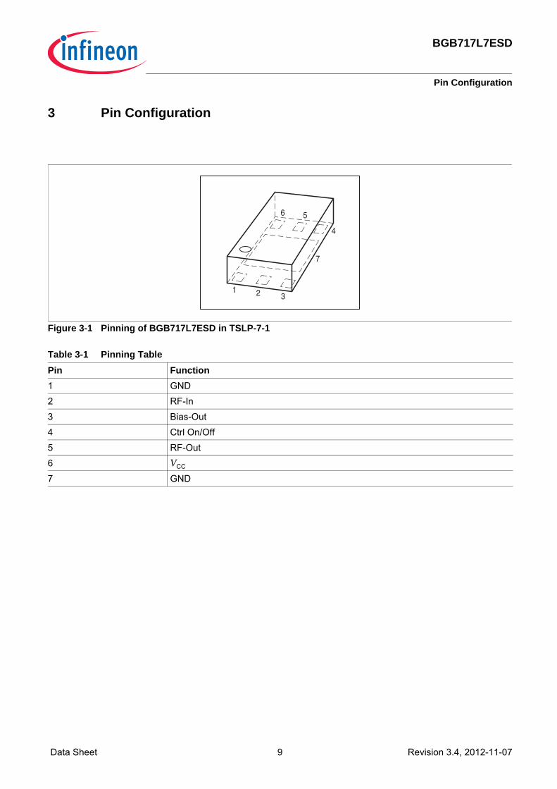
3 Pin Configuration
Figure 3-1 Pinning of BGB717L7ESD in TSLP-7-1
Table 3-1 Pinning TablePin Function1 GND2 RF-In3 Bias-Out4 Ctrl On/Off5 RF-Out6 VCC
7 GND
1 2 3
6 5
4
7

BGB717L7ESD
Maximum Ratings
Data Sheet 10 Revision 3.4, 2012-11-07
4 Maximum Ratings
Attention: Stresses above the max. values listed here may cause permanent damage to the device. Exposure to absolute maximum rating conditions for extended periods may affect device reliability. Maximum ratings are absolute ratings; exceeding only one of these values may cause irreversible damage to the integrated circuit.
Table 4-1 Maximum Ratings at TA = 25 °CParameter Symbol Value Unit Note / Test
Condition Min. Typ. Max.Supply voltage VCC – – 4.0 V TA = 25 °C
– 3.5 TA = -55 °CSupply current at VCC pin ICC – – 25 mA –IDC current at RF-In Pin IB – – 3 mA –Control On / Off voltage Vctrl – – 4.0 V –Total power dissipation1)
1) TS is the soldering point temperature. TS is measured at the GND pin (7) at the soldering point to the pcb
Ptot – – 100 mW TS ≤ 112 °CJunction temperature TJ – – 150 °C –Storage temperature TStg -55 – 150 °C –ESD CapabilityHuman Body Model JESD22-A114-B – – – 2000 V –Machine Model JESD22-A115-A – – – 100 V –Charge Device Model JESD22-C101-C – – – 1500 V –

BGB717L7ESD
Thermal Characteristics
Data Sheet 11 Revision 3.4, 2012-11-07
5 Thermal Characteristics
Figure 5-1 Total Power Dissipation Ptot = f (Ts)
6 Operation Conditions
Table 5-1 Thermal ResistanceParameter Symbol Values Unit Note / Test Condition
Min. Typ. Max.Junction - soldering point1)
1)For the definition of RthJS please refer to Application Note AN077 (Thermal Resistance Calculation)RthJS – 375 – K/W –
Table 6-1 Operation ConditionsParameter Symbol Values Unit Note / Test Condition
Min. Typ. Max.Supply voltage VCC 1.8 3.0 4.0 V –Voltage Ctrl On/Off pin in On mode Vctrl-on 1.2 3.0 VCC V –Voltage Ctrl On/Off pin in Off mode Vctrl-off -0.3 0 0.3 V –
0
20
40
60
80
100
120
0 50 100 150
Ts [°C]
Ptot
[mW
]
BGB717L7ESD
Electrical Characteristics
Data Sheet 12 Revision 3.4, 2012-11-07
7 Electrical Characteristics
7.1 DC Characteristics
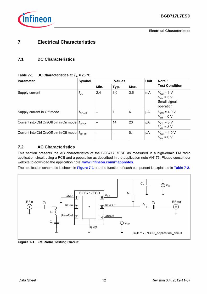
7.2 AC CharacteristicsThis section presents the AC characteristics of the BGB717L7ESD as measured in a high-ohmic FM radioapplication circuit using a PCB and a population as described in the application note AN176. Please consult ourwebsite to download the application note: www.infineon.com/rf.appnotes.The application schematic is shown in Figure 7-1 and the function of each component is explained in Table 7-2.
Figure 7-1 FM Radio Testing Circuit
Table 7-1 DC Characteristics at TA = 25 °CParameter Symbol Values Unit Note /
Test ConditionMin. Typ. Max.Supply current ICC 2.4 3.0 3.6 mA VCC = 3 V
Vctrl = 3 VSmall signal operation
Supply current in Off mode ICC-off – 1 6 µA VCC = 4.0 VVctrl = 0 V
Current into Ctrl On/Off pin in On mode Ictrl-on – 14 20 µA VCC = 3 VVctrl = 3 V
Current into Ctrl On/Off pin in Off mode Ictrl-off – – 0.1 µA VCC = 4.0 VVctrl = 0 V
2
3
6
5
4
1
VCC
RF-In
On/OffBias-Out
RF-Out
GND
R1
RFin
BGB717ESD
7
C3
VCC
C1
L1
C2 VCtrl
C4R2
RFout
GND
BGB717L7ESD_Application_circuit

BGB717L7ESD
Electrical Characteristics
Data Sheet 13 Revision 3.4, 2012-11-07
The following table gives an overview on the performance of the FM radio LNA application circuit. All data weremeasured in a 50 Ω system.
Table 7-2 Bill of MaterialComponent Value Manufacturer / Type FunctionC1 330 pF Various / 0402 DC blockingC2 47 nF Various / 0402 DC stabilizationC3 47 nF Various / 0402 DC stabilizationC4 330 pF Various / 0402 DC blockingR1 56 Ω Various / 0402 For biasing, output
matching and stabilizationR2 10 Ω Various / 0402 For output matching and
stabilizationL1 470 nH Taiyo Yuden LK1608R47K-T /
0603RF choke
Table 7-3 AC Characteristics in the FM Radio LNA Application1)
1) As described in AN176, TA = 25 °C, VCC = 3 V, Vctrl = 3 V, ICC = 3 mA, f = 100 MHz
Parameter Symbol Values Unit Note / Test ConditionMin. Typ. Max.
Insertion power gain |S21|2 10 12 14 dB –Input return loss2)
2) Verified by random sampling
RLIN 0 0.53)
3) High LNA input impedance leads to power matching with high ohmic antennas
3 dB –Output return loss2) RLOUT 13 164)
4) Output matching is accomplished by the external resistors R1 and R2
19 dB –Noise figure5)
5) An aggressive low pass filter prevents radio broadcast signals from distorting the NF measurement
NF50 – 1.0 1.5 dB Zs = 50 ΩInput 1dB gain compression point2) IP-1dB -8.0 -5.5 – dBm –Input 3rd Order Intercept Point2) IIP3 -15.5 -12.5 – dBm PRFIN = -40 dBm
BGB717L7ESD
Package Information TSLP-7-1
Data Sheet 14 Revision 3.4, 2012-11-07
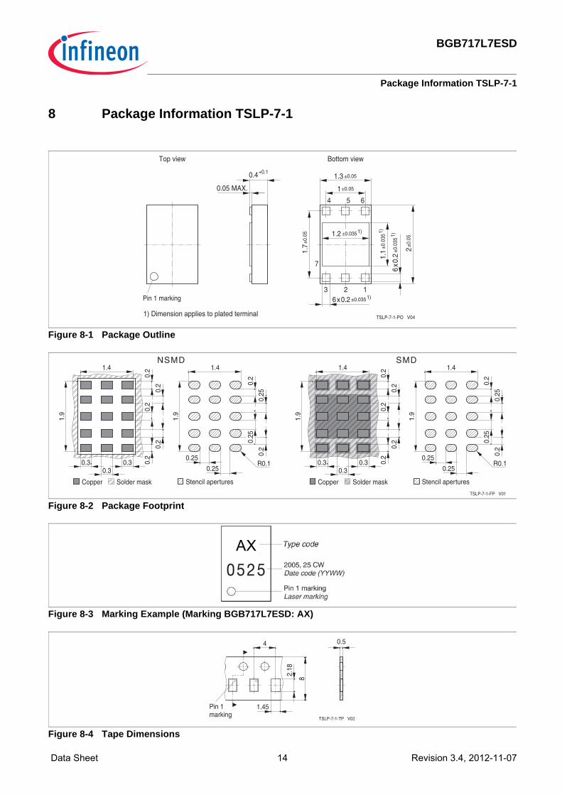
8 Package Information TSLP-7-1
Figure 8-1 Package Outline
Figure 8-2 Package Footprint
Figure 8-3 Marking Example (Marking BGB717L7ESD: AX)
Figure 8-4 Tape Dimensions
0.05 MAX.
+0.10.4
1) Dimension applies to plated terminal
±0.0351.2
±0.051
±0.051.3
±0.0
51.
7 ±0.0
52
6 x0.2 ±0.0351)
6x0
.2±0
.035
1)
±0.0
351.
11)
4 5 6
123
7
1)
Top view Bottom view
Pin 1 marking
TSLP-7-1-PO V04
0.25
1.4
1.9
0.25
0.2
0.25
0.25
0.2
1.4
1.9
0.3 0.30.3
0.2
0.2
0.2
0.2
0.2
Stencil aperturesCopper Solder mask
R0.10.25
1.4
1.9
0.25
0.2
0.25
0.25
0.2
1.4
1.9
0.3 0.30.3
0.2
0.2
0.2
0.2
0.2
Stencil aperturesCopper Solder mask
R0.1
SMDNSMD
TSLP-7-1-FP V01
AXAX
TSLP-7-1-TP V03
1.45
4
8
2.18
0.5
Pin 1 marking

Mouser Electronics
Authorized Distributor
Click to View Pricing, Inventory, Delivery & Lifecycle Information: Infineon:
BGB 717L7ESD E6327 BGB 717L7ESD E6433