Embed Size (px)
Citation preview
Data Sheet 1 Rev. 1.00www.infineon.com 2016-09-20
BTS7008-2EPA
1 Overview
Application
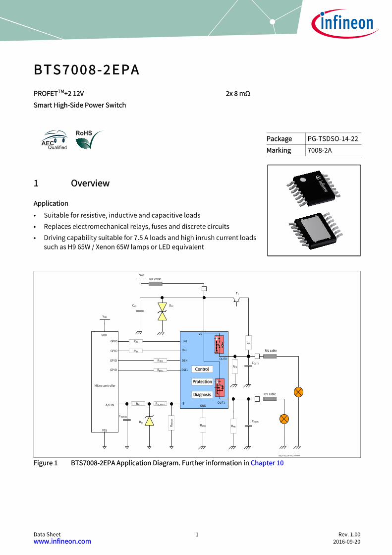
• Suitable for resistive, inductive and capacitive loads• Replaces electromechanical relays, fuses and discrete circuits• Driving capability suitable for 7.5 A loads and high inrush current loads
such as H9 65W / Xenon 65W lamps or LED equivalent
Figure 1 BTS7008-2EPA Application Diagram. Further information in Chapter 10
PROFETTM+2 12V 2x 8 mΩ
Smart High-Side Power Switch
Package PG-TSDSO-14-22
Marking 7008-2A
GPIO
GPIO
GPIO
GPIO
A/D IN
VSS
VDD
Micro controller
IN0
IN1
DEN
DSEL
ISGND
OUT0
OUT1
VS
VBAT
CSENSE
DZ1
R/L cable
R/L cable
R/L cable
COUT1
COUT0
RIN
RIN
RDEN
RDSEL
RAD RIS_PROT
R SEN
SE
RGND
VDD
RPD
RPD
CVS
ROL
T1
DZ2
App_2CH_LI_INTDIO_Cover.emf
Control
Protection
Diagnosis
T
T

Data Sheet 2 Rev. 1.00 2016-09-20
BTS7008-2EPAPROFETTM+2 12V
Overview
Basic Features
• High Side Switch with Diagnosis and Embedded Protection• Part of PROFETTM+2 12V Family• ReverSave™ for low power dissipation in Reverse Polarity• Green Product (RoHS compliant)• Qualified in accordance with AEC Q100 grade 1
Protection Features
• Absolute and dynamic temperature limitation with controlled restart • Over Current protection (tripping) with Intelligent Restart Control• Under Voltage shutdown• Over Voltage Protection with external components
Diagnostic Features
• Proportional load current sense• Open Load in ON and OFF state• Short circuit to ground and battery
Description
The BTS7008-2EPA is a Smart High-Side Power Switch 8 mΩ Dual channel, providing protection functions anddiagnosis. The device is integrated in SMART7 technology.
Table 1 Product Summary
Parameter Symbol Values
Minimum Operating voltage (at switch ON) VS(OP) 4.1 V
Minimum Operating voltage (cranking) VS(UV) 3.1 V
Maximum Operating voltage VS 28 V
Minimum overvoltage protection @ 25 °C VDS(CLAMP) 35 V
Maximum current in Sleep mode (TJ ≤ 85 °C) IVS(SLEEP) 0.6 µA
Maximum operative current IGND(ACTIVE) 5 mA
Maximum ON-state resistance (TJ = 150 °C) RDS(ON) 16 mΩ
Nominal load current (TA = 85 °C) IL(NOM) 7.5 A
Typical current sense ratio at IL = IL(NOM) kILIS 5500
Data Sheet 3 Rev. 1.00 2016-09-20
BTS7008-2EPAPROFETTM+2 12V
Block Diagram and Terms
2 Block Diagram and Terms
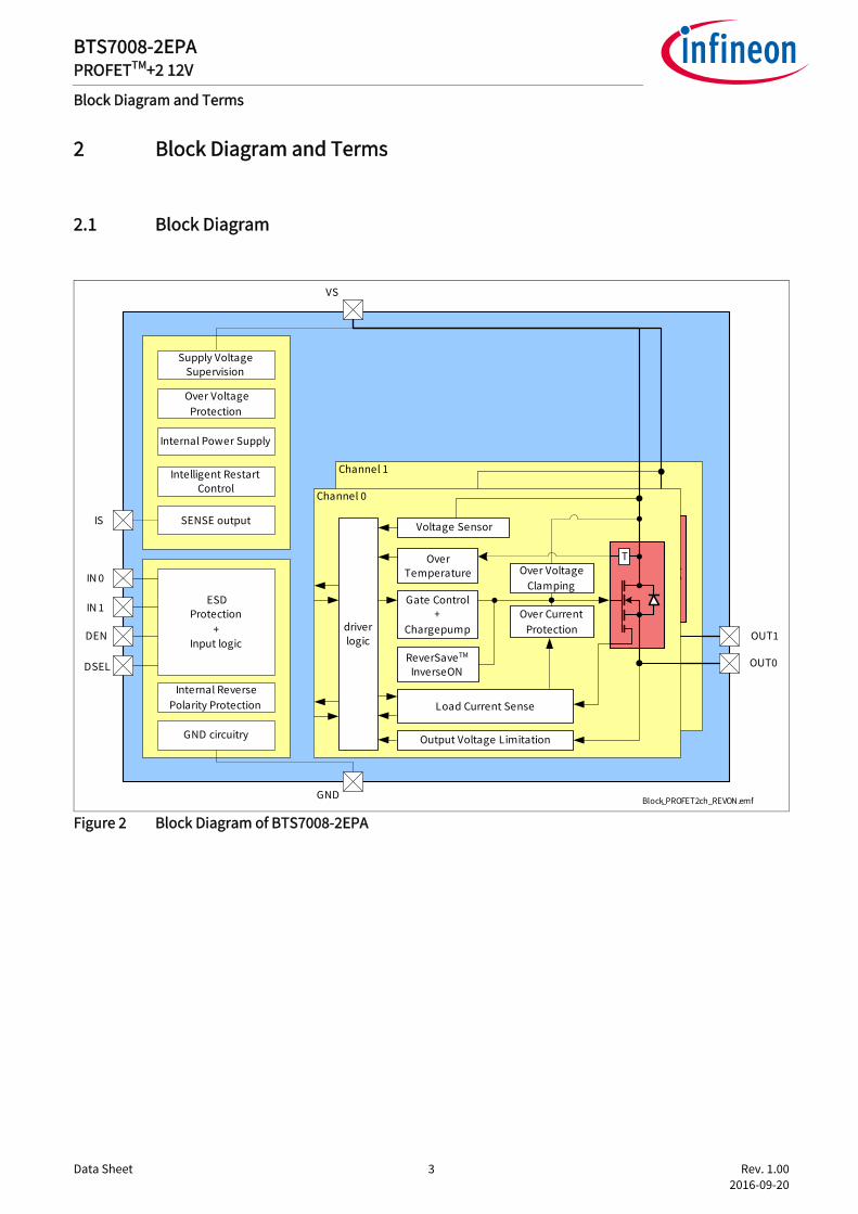
2.1 Block Diagram
Figure 2 Block Diagram of BTS7008-2EPA
IN 0
ESDProtection
+Input logic
IS
DEN
DSEL
IN 1
Internal Power Supply
Block_PROFET2ch_REVON.emf
GND circuitry
Supply Voltage Supervision
Over Voltage Protection
Intelligent Restart Control
SENSE output
VS
GND
OUT1
OUT0
Internal Reverse Polarity Protection
Channel 1
T
driver logic
Gate Control+
Chargepump
Load Current Sense
Over Temperature Over Voltage
Clamping
Over CurrentProtection
Output Voltage Limitation
Voltage Sensor
ReverSaveTM
InverseON
Channel 0
T
driver logic
Gate Control+
Chargepump
Load Current Sense
Over Temperature Over Voltage
Clamping
Over CurrentProtection
Output Voltage Limitation
Voltage Sensor
ReverSaveTM
InverseON
Data Sheet 4 Rev. 1.00 2016-09-20
BTS7008-2EPAPROFETTM+2 12V
Block Diagram and Terms
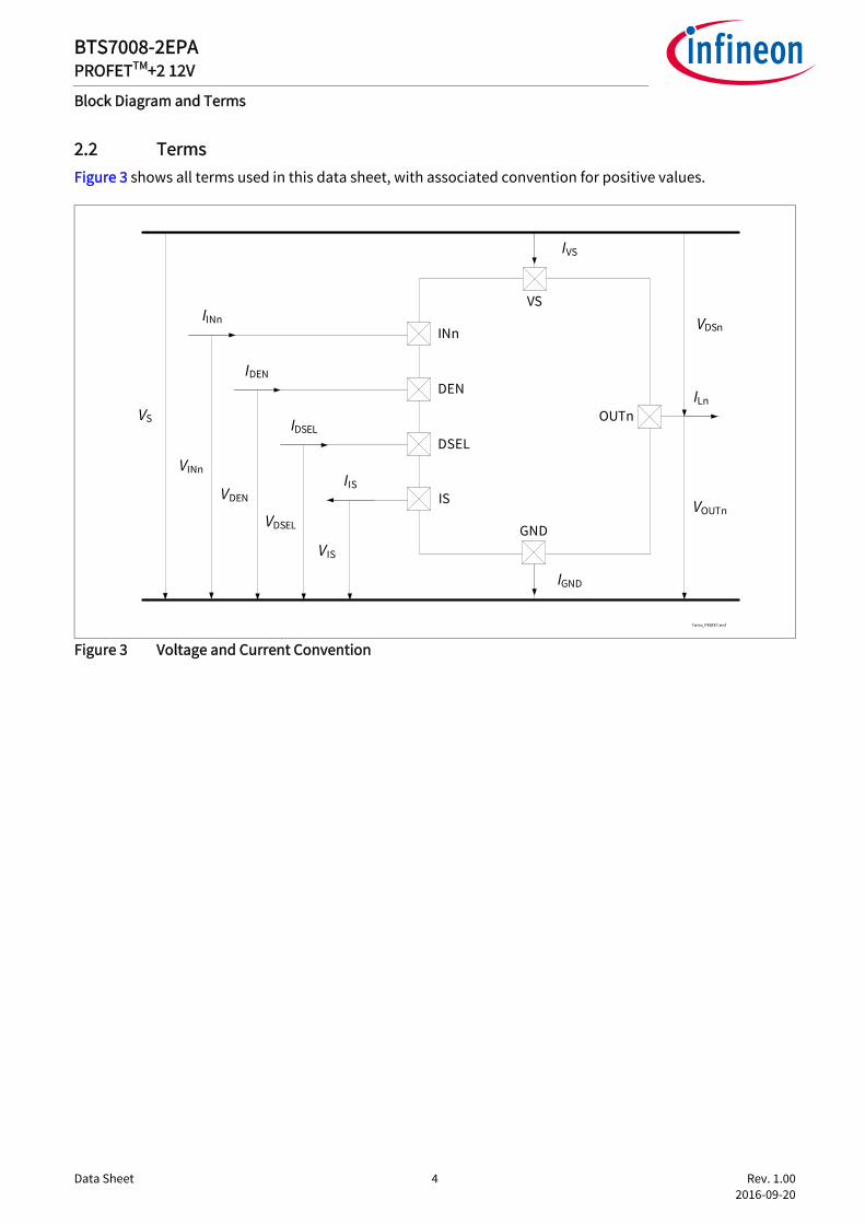
2.2 TermsFigure 3 shows all terms used in this data sheet, with associated convention for positive values.
Figure 3 Voltage and Current Convention
IINn
IDEN
IIS
VS
IGND
ILn
IDSEL
INn
DEN
DSEL
IS
GND
VS
OUTn
VINn
VDEN
VDSEL
VIS
VOUTn
VDSn
IVS
Terms_PROFET.emf
Data Sheet 5 Rev. 1.00 2016-09-20
BTS7008-2EPAPROFETTM+2 12V
Pin Configuration
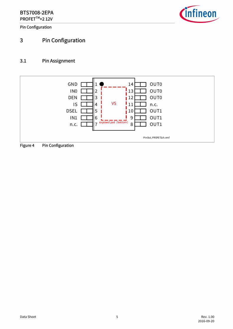
3 Pin Configuration
3.1 Pin Assignment
Figure 4 Pin Configuration
VS
GND OUT0IN0
DENIS
DSELIN1n.c.
OUT0OUT0n.c.OUT1OUT1OUT1
1234567
1413121110
98
PinOut_PROFET2ch.emf
exposed pad (bottom)

Data Sheet 6 Rev. 1.00 2016-09-20
BTS7008-2EPAPROFETTM+2 12V
Pin Configuration
3.2 Pin Definitions and Functions
Table 2 Pin Definition
Pin Symbol Function
EP VS(exposed pad)
Supply VoltageBattery voltage
1 GND GroundSignal ground
2, 6 INn Input Channel nDigital signal to switch ON channel n (“high” active)If not used: connect to GND pin or to module ground with a 10 kΩ resistor
3 DEN Diagnostic EnableDigital signal to enable device diagnosis (“high” active) and to clear the protection counter of channel selected with DSEL pinIf not used: connect to GND pin or to module ground with a 10 kΩ resistor
4 IS SENSE current outputAnalog/digital signal for diagnosisIf not used: left open
5 DSEL Diagnosis Selection Digital signal to select one channel to perform ON and OFF state diagnosis (“high” active)If not used: connect to GND pin or to module ground with a 10 kΩ resistor
7, 11 n.c. Not connected, internally not bonded
8-10, 12-14
OUTn Output nProtected high-side power output channel n1)
1) All output pins of the channel must be connected together on the PCB. All pins of the output are internally connected together. PCB traces have to be designed to withstand the maximum current which can flow
Data Sheet 7 Rev. 1.00 2016-09-20
BTS7008-2EPAPROFETTM+2 12V
General Product Characteristics
4 General Product Characteristics
4.1 Absolute Maximum Ratings - General
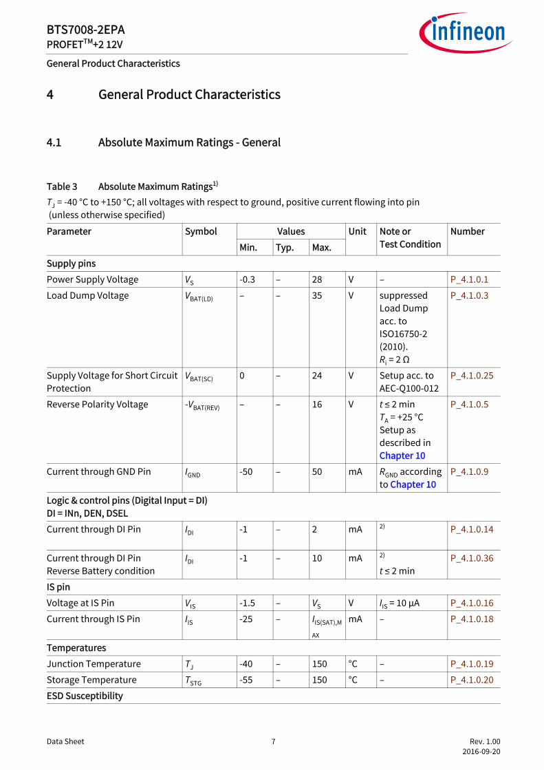
Table 3 Absolute Maximum Ratings1)
TJ = -40 °C to +150 °C; all voltages with respect to ground, positive current flowing into pin (unless otherwise specified)
Parameter Symbol Values Unit Note or Test Condition
Number
Min. Typ. Max.
Supply pins
Power Supply Voltage VS -0.3 – 28 V – P_4.1.0.1
Load Dump Voltage VBAT(LD) – – 35 V suppressed Load Dump acc. to ISO16750-2 (2010).Ri = 2 Ω
P_4.1.0.3
Supply Voltage for Short Circuit Protection
VBAT(SC) 0 – 24 V Setup acc. to AEC-Q100-012
P_4.1.0.25
Reverse Polarity Voltage -VBAT(REV) – – 16 V t ≤ 2 minTA = +25 °CSetup as described in Chapter 10
P_4.1.0.5
Current through GND Pin IGND -50 – 50 mA RGND according to Chapter 10
P_4.1.0.9
Logic & control pins (Digital Input = DI)DI = INn, DEN, DSEL
Current through DI Pin IDI -1 – 2 mA 2) P_4.1.0.14
Current through DI PinReverse Battery condition
IDI -1 – 10 mA 2)
t ≤ 2 minP_4.1.0.36
IS pin
Voltage at IS Pin VIS -1.5 – VS V IIS = 10 μA P_4.1.0.16
Current through IS Pin IIS -25 – IIS(SAT),M
AX
mA – P_4.1.0.18
Temperatures
Junction Temperature TJ -40 – 150 °C – P_4.1.0.19
Storage Temperature TSTG -55 – 150 °C – P_4.1.0.20
ESD Susceptibility
Data Sheet 8 Rev. 1.00 2016-09-20
BTS7008-2EPAPROFETTM+2 12V
General Product Characteristics
Notes
1. Stresses above the ones listed here may cause permanent damage to the device. Exposure to absolute maximum rating conditions for extended periods may affect device reliability.
2. Integrated protection functions are designed to prevent IC destruction under fault conditions described in the data sheet. Fault conditions are considered as “outside” normal operating range. Protection functions are not designed for continuous repetitive operation.
4.2 Absolute Maximum Ratings - Power Stages
4.2.1 Power Stage - 8 mΩ
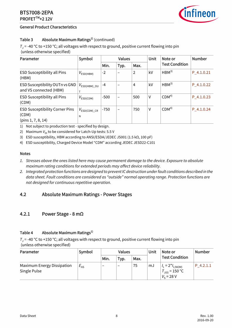
ESD Susceptibility all Pins (HBM)
VESD(HBM) -2 – 2 kV HBM3) P_4.1.0.21
ESD Susceptibility OUTn vs GND and VS connected (HBM)
VESD(HBM)_OU
T
-4 – 4 kV HBM3) P_4.1.0.22
ESD Susceptibility all Pins (CDM)
VESD(CDM) -500 – 500 V CDM4) P_4.1.0.23
ESD Susceptibility Corner Pins (CDM)(pins 1, 7, 8, 14)
VESD(CDM)_CR
N
-750 – 750 V CDM4) P_4.1.0.24
1) Not subject to production test - specified by design.2) Maximum VDI to be considered for Latch-Up tests: 5.5 V3) ESD susceptibility, HBM according to ANSI/ESDA/JEDEC JS001 (1.5 kΩ, 100 pF)4) ESD susceptibility, Charged Device Model “CDM” according JEDEC JESD22-C101
Table 4 Absolute Maximum Ratings1)
TJ = -40 °C to +150 °C; all voltages with respect to ground, positive current flowing into pin (unless otherwise specified)
Parameter Symbol Values Unit Note or Test Condition
Number
Min. Typ. Max.
Maximum Energy DissipationSingle Pulse
EAS – – 75 mJ IL = 2*IL(NOM)TJ(0) = 150 °CVS = 28 V
P_4.2.1.1
Table 3 Absolute Maximum Ratings1) (continued)TJ = -40 °C to +150 °C; all voltages with respect to ground, positive current flowing into pin (unless otherwise specified)
Parameter Symbol Values Unit Note or Test Condition
Number
Min. Typ. Max.
Data Sheet 9 Rev. 1.00 2016-09-20
BTS7008-2EPAPROFETTM+2 12V
General Product Characteristics
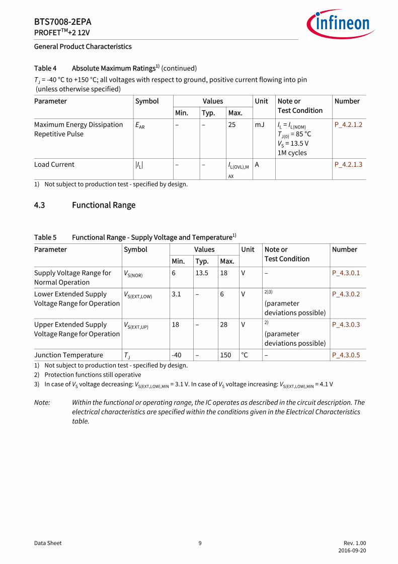
4.3 Functional Range
Note: Within the functional or operating range, the IC operates as described in the circuit description. The electrical characteristics are specified within the conditions given in the Electrical Characteristics table.
Maximum Energy DissipationRepetitive Pulse
EAR – – 25 mJ IL = IL(NOM)TJ(0) = 85 °CVS = 13.5 V1M cycles
P_4.2.1.2
Load Current |IL| – – IL(OVL),M
AX
A P_4.2.1.3
1) Not subject to production test - specified by design.
Table 5 Functional Range - Supply Voltage and Temperature1)
1) Not subject to production test - specified by design.
Parameter Symbol Values Unit Note or Test Condition
Number
Min. Typ. Max.
Supply Voltage Range for Normal Operation
VS(NOR) 6 13.5 18 V – P_4.3.0.1
Lower Extended Supply Voltage Range for Operation
VS(EXT,LOW) 3.1 – 6 V 2)3)
(parameter deviations possible)
2) Protection functions still operative3) In case of VS voltage decreasing: VS(EXT,LOW),MIN = 3.1 V. In case of VS voltage increasing: VS(EXT,LOW),MIN = 4.1 V
P_4.3.0.2
Upper Extended Supply Voltage Range for Operation
VS(EXT,UP) 18 – 28 V 2)
(parameter deviations possible)
P_4.3.0.3
Junction Temperature TJ -40 – 150 °C – P_4.3.0.5
Table 4 Absolute Maximum Ratings1) (continued)TJ = -40 °C to +150 °C; all voltages with respect to ground, positive current flowing into pin (unless otherwise specified)
Parameter Symbol Values Unit Note or Test Condition
Number
Min. Typ. Max.
Data Sheet 10 Rev. 1.00 2016-09-20
BTS7008-2EPAPROFETTM+2 12V
General Product Characteristics
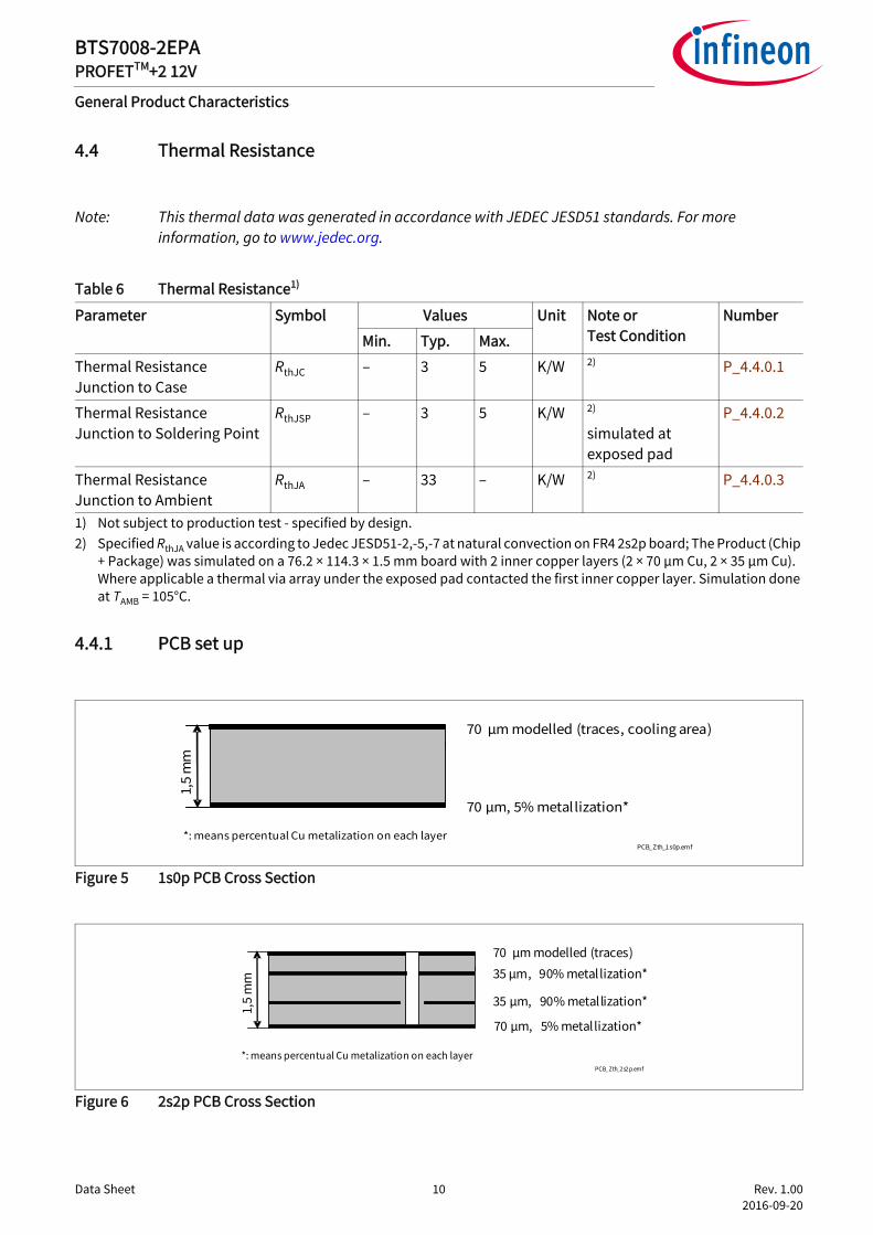
4.4 Thermal Resistance
Note: This thermal data was generated in accordance with JEDEC JESD51 standards. For more information, go to www.jedec.org.
4.4.1 PCB set up
Figure 5 1s0p PCB Cross Section
Figure 6 2s2p PCB Cross Section
Table 6 Thermal Resistance1)
1) Not subject to production test - specified by design.
Parameter Symbol Values Unit Note or Test Condition
Number
Min. Typ. Max.
Thermal Resistance Junction to Case
RthJC – 3 5 K/W 2)
2) Specified RthJA value is according to Jedec JESD51-2,-5,-7 at natural convection on FR4 2s2p board; The Product (Chip + Package) was simulated on a 76.2 × 114.3 × 1.5 mm board with 2 inner copper layers (2 × 70 µm Cu, 2 × 35 µm Cu). Where applicable a thermal via array under the exposed pad contacted the first inner copper layer. Simulation done at TAMB = 105°C.
P_4.4.0.1
Thermal Resistance Junction to Soldering Point
RthJSP – 3 5 K/W 2)
simulated at exposed pad
P_4.4.0.2
Thermal Resistance Junction to Ambient
RthJA – 33 – K/W 2) P_4.4.0.3
70 µm modelled (traces, cooling area)
1,5
mm
70 µm, 5% metallization*
PCB_Zth_1s0p.emf*: means percentual Cu metalization on each layer
70 µm modelled (traces)
35 µm, 90% metallization*1,5
mm
70 µm, 5% metallization*
PCB_Zth_2s2p.emf
35 µm, 90% metallization*
*: means percentual Cu metalization on each layer
Data Sheet 11 Rev. 1.00 2016-09-20
BTS7008-2EPAPROFETTM+2 12V
General Product Characteristics
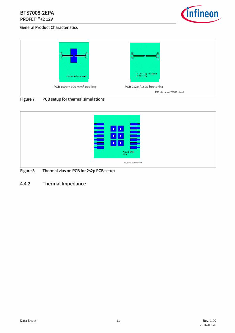
Figure 7 PCB setup for thermal simulations
Figure 8 Thermal vias on PCB for 2s2p PCB setup
4.4.2 Thermal Impedance
PCB_sim _setup_TSDSO14.emf
PCB 1s0p + 600 mm² cooling PCB 2s2p / 1s0p footprint
PCB_2s2p_vias_TSDSO14.emf
Data Sheet 12 Rev. 1.00 2016-09-20
BTS7008-2EPAPROFETTM+2 12V
General Product Characteristics
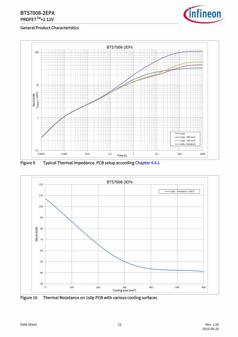
Figure 9 Typical Thermal Impedance. PCB setup according Chapter 4.4.1
Figure 10 Thermal Resistance on 1s0p PCB with various cooling surfaces
0.1
1
10
100
0.0001 0.001 0.01 0.1 1 10 100 1000
Zth
JA (K
/W)
TA
MB
IEN
T=
10
5°C
Time (s)
BTS7008-2EPx
2s2p
1s0p - 600 mm
1s0p - 300 mm
1s0p - footprint
30
40
50
60
70
80
90
100
110
120
0 100 200 300 400 500 600
Rth
JA (K
/W)
Cooling area (mm)
BTS7008-2EPx
1s0p - Tambient = 105°C
Data Sheet 13 Rev. 1.00 2016-09-20
BTS7008-2EPAPROFETTM+2 12V
Logic Pins
5 Logic PinsThe device has 4 digital pins for direct control.
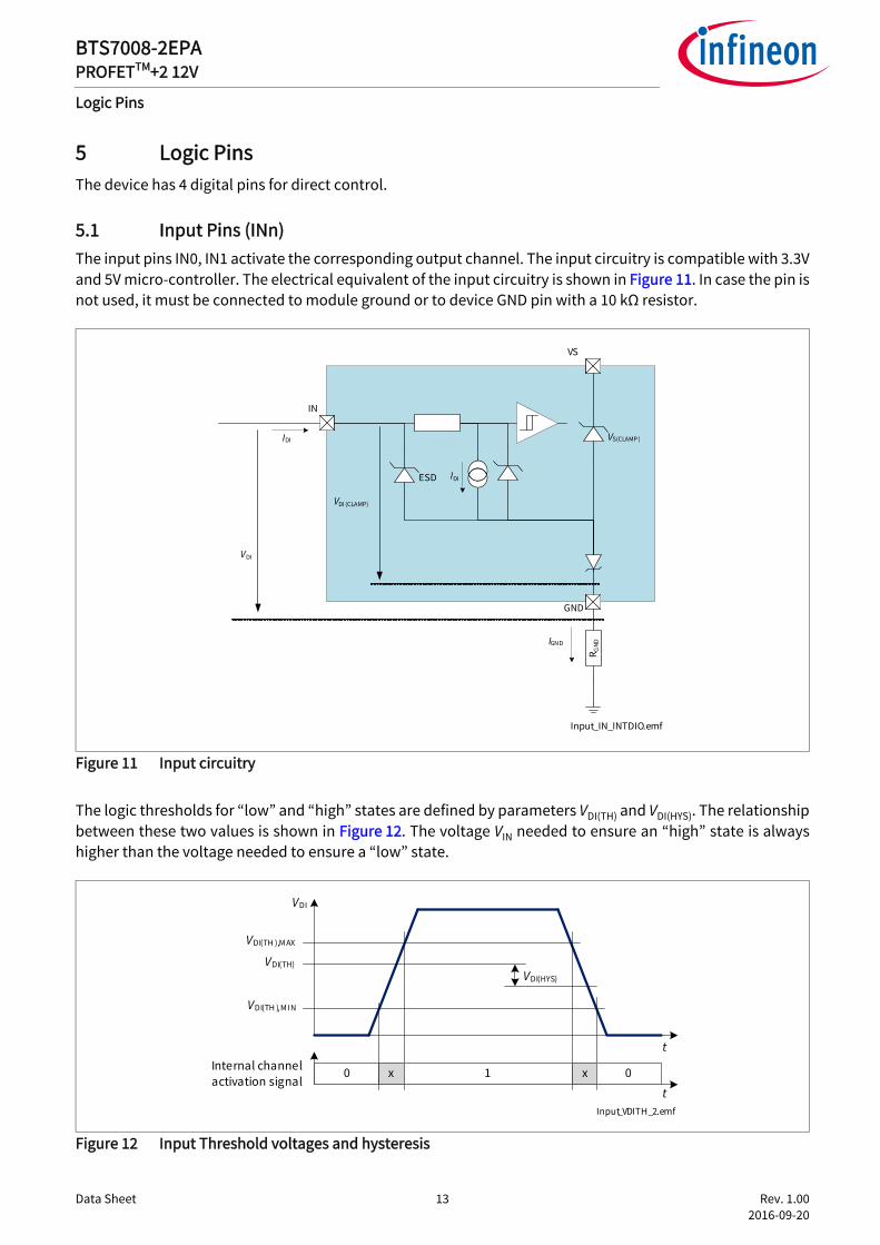
5.1 Input Pins (INn)The input pins IN0, IN1 activate the corresponding output channel. The input circuitry is compatible with 3.3Vand 5V micro-controller. The electrical equivalent of the input circuitry is shown in Figure 11. In case the pin isnot used, it must be connected to module ground or to device GND pin with a 10 kΩ resistor.
Figure 11 Input circuitry
The logic thresholds for “low” and “high” states are defined by parameters VDI(TH) and VDI(HYS). The relationshipbetween these two values is shown in Figure 12. The voltage VIN needed to ensure an “high” state is alwayshigher than the voltage needed to ensure a “low” state.
Figure 12 Input Threshold voltages and hysteresis
GND
IN
IGND
IDI
VDI
Input_IN_INTDIO.emf
VS
VS(CLAMP )
R GND
IDIESD
VDI (CLAMP)
Input_VDITH_2.emf
VDI(TH ),M AX
VDI(HYS)
t
VDI
VDI(TH ),M IN
Internal channel activation signal
t0 x 1 x 0
VDI(TH)

Data Sheet 14 Rev. 1.00 2016-09-20
BTS7008-2EPAPROFETTM+2 12V
Logic Pins
5.2 Diagnosis PinThe Diagnosis Enable (DEN) pin controls the diagnosis circuitry and the protection circuitry. When DEN pin isset to “high”, the diagnosis is enabled (see Chapter 9.2 for more details). When it is set to “low”, the diagnosisis disabled (IS pin is set to high impedance).The Diagnosis Selection (DSEL) pin selects the channel where diagnosis is performed (see Chapter 9.1.1).The transition from “high” to “low” of DEN pin clears the protection latch of the channel selected with DSELpin depending on the logic state of IN pin and DEN pulse length (see Chapter 8.3 for more details). The internalstructure of diagnosis pins is the same as the one of input pins. See Figure 11 for more details.
Data Sheet 15 Rev. 1.00 2016-09-20
BTS7008-2EPAPROFETTM+2 12V
Logic Pins
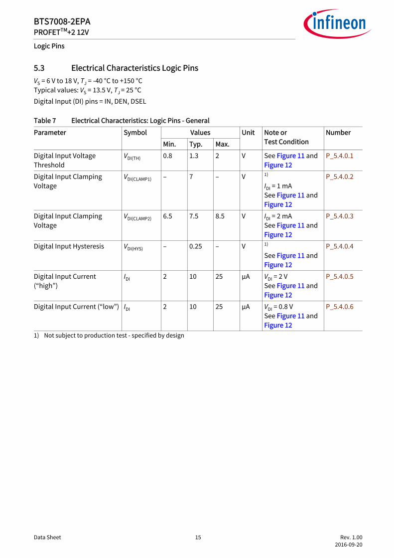
5.3 Electrical Characteristics Logic PinsVS = 6 V to 18 V, TJ = -40 °C to +150 °CTypical values: VS = 13.5 V, TJ = 25 °CDigital Input (DI) pins = IN, DEN, DSEL
Table 7 Electrical Characteristics: Logic Pins - General
Parameter Symbol Values Unit Note or Test Condition
Number
Min. Typ. Max.
Digital Input Voltage Threshold
VDI(TH) 0.8 1.3 2 V See Figure 11 and Figure 12
P_5.4.0.1
Digital Input Clamping Voltage
VDI(CLAMP1) – 7 – V 1)
IDI = 1 mASee Figure 11 and Figure 12
1) Not subject to production test - specified by design
P_5.4.0.2
Digital Input Clamping Voltage
VDI(CLAMP2) 6.5 7.5 8.5 V IDI = 2 mASee Figure 11 and Figure 12
P_5.4.0.3
Digital Input Hysteresis VDI(HYS) – 0.25 – V 1)
See Figure 11 and Figure 12
P_5.4.0.4
Digital Input Current (“high”)
IDI 2 10 25 µA VDI = 2 VSee Figure 11 and Figure 12
P_5.4.0.5
Digital Input Current (“low”) IDI 2 10 25 µA VDI = 0.8 VSee Figure 11 and Figure 12
P_5.4.0.6
Data Sheet 16 Rev. 1.00 2016-09-20
BTS7008-2EPAPROFETTM+2 12V
Power Supply
6 Power SupplyThe BTS7008-2EPA is supplied by VS, which is used for the internal logic as well as supply for the power outputstages. VS has an undervoltage detection circuit, which prevents the activation of the power output stages anddiagnosis in case the applied voltage is below the undervoltage threshold.
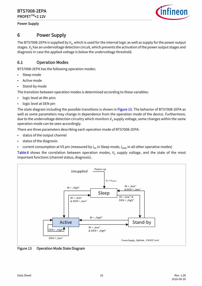
6.1 Operation ModesBTS7008-2EPA has the following operation modes:• Sleep mode • Active mode • Stand-by mode The transition between operation modes is determined according to these variables:• logic level at INn pins• logic level at DEN pinThe state diagram including the possible transitions is shown in Figure 13. The behavior of BTS7008-2EPA aswell as some parameters may change in dependence from the operation mode of the device. Furthermore,due to the undervoltage detection circuitry which monitors VS supply voltage, some changes within the sameoperation mode can be seen accordingly.There are three parameters describing each operation mode of BTS7008-2EPA:• status of the output channel• status of the diagnosis• current consumption at VS pin (measured by IVS in Sleep mode, IGND in all other operative modes)Table 8 shows the correlation between operation modes, VS supply voltage, and the state of the mostimportant functions (channel status, diagnosis).
Figure 13 Operation Mode State Diagram
PowerSupply_OpMode _PROFET.emf
Sleep
Active
IN = „high“
IN = „low“ &DEN = „high“
Stand-by
IN = „low“& DEN = „low“
Power-up
IN = „low“& DEN = „high“
IN = „low“& DEN = „low“
VS > VS(OP )
Unsupplied
IN = „high“
DEN = „high“
DEN = „low“
Data Sheet 17 Rev. 1.00 2016-09-20
BTS7008-2EPAPROFETTM+2 12V
Power Supply
6.1.1 UnsuppliedIn this state, the device is either unsupplied (no voltage applied to VS pin) or the supply voltage is below theundervoltage threshold.
6.1.2 Power-upThe Power-up condition is entered when the supply voltage (VS) is applied to the device. The supply is risinguntil it is above the undervoltage threshold VS(OP) therefore the internal power-on signals are set.
6.1.3 Sleep modeThe device is in Sleep mode when all Digital Input pins (INn, DEN, DSEL) are set to “low”. When BTS7008-2EPAis in Sleep mode, all outputs are OFF. The current consumption is minimum (see parameter IVS(SLEEP)). No OverTemperature or Overload protection mechanism is active when the device is in Sleep mode. The device cango in Sleep mode only if the protection is not active (counter = 0, see Chapter 8.3.1 for further details).
6.1.4 Stand-by modeThe device is in Stand-by mode as long as DEN pin is set to “high” while input pins are set to “low”. All channelsare OFF therefore only Open Load in OFF diagnosis is possible. Depending on the load condition, either a faultcurrent IIS(FAULT) or an Open Load in OFF current IIS(OLOFF) may be present at IS pin. In such situation, the currentconsumption of the device is increased.
6.1.5 Active modeActive mode is the normal operation mode of BTS7008-2EPA. The device enters Active mode as soon as one INpin is set to “high”. Device current consumption is specified with IGND(ACTIVE) (measured at GND pin because thecurrent at VS pin includes the load current). Overload, Over Temperature and Over Voltage protections areactive. Diagnosis is available.
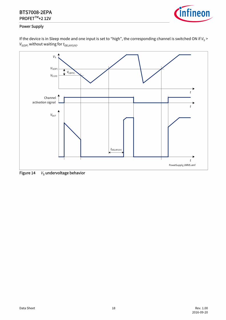
6.2 Undervoltage on VS
Between VS(OP) and VS(UV) the undervoltage mechanism is triggered. If the device is operative (in Active mode)and the supply voltage drops below the undervoltage threshold VS(UV), the internal logic switches OFF theoutput channels.As soon as the supply voltage VS is above the operative threshold VS(OP), the channels having the correspondinginput pin set to “high” are switched ON again. The restart is delayed with a time tDELAY(UV) which protects thedevice in case the undervoltage condition is caused by a short circuit event (according to AEC-Q100-012), asshown in Figure 14.
Table 8 Device function in relation to operation modes and VS voltage
Operative Mode Function VS in undervoltage VS not in undervoltage
Sleep Channel OFF OFF
Diagnosis OFF OFF
Active Channels OFF available
Diagnosis OFF available in OFF and ON states
Stand-by Channels OFF OFF
Diagnosis OFF available in OFF state
Data Sheet 18 Rev. 1.00 2016-09-20
BTS7008-2EPAPROFETTM+2 12V
Power Supply
If the device is in Sleep mode and one input is set to “high”, the corresponding channel is switched ON if VS >VS(OP) without waiting for tDELAY(UV).
Figure 14 VS undervoltage behavior
PowerSupply_UVRVS.emf
t
VS(OP)
VS (UV)
VS (HYS )
t
VOUT
VS
tDELAY(UV )
Channel activation signal
t
Data Sheet 19 Rev. 1.00 2016-09-20
BTS7008-2EPAPROFETTM+2 12V
Power Supply
6.3 Electrical Characteristics Power SupplyVS = 6 V to 18 V, TJ = -40 °C to +150 °CTypical values: VS = 13.5 V, TJ = 25 °CTypical resistive loads connected to the outputs for testing (unless otherwise specified):RL = 3.3 Ω
6.4 Electrical Characteristics Power Supply - product specific
6.4.1 BTS7008-2EPA
Table 9 Electrical Characteristics: Power Supply - General
Parameter Symbol Values Unit Note or Test Condition
Number
Min. Typ. Max.
VS pin
Power Supply Undervoltage Shutdown
VS(UV) 1.8 2.3 3.1 V VS decreasingIN = “high” From VDS ≤ 0.5 V to VDS = VSSee Figure 14
P_6.4.0.1
Power Supply Minimum Operating Voltage
VS(OP) 2.0 3.0 4.1 V VS increasingIN = “high”From VDS = VS to VDS ≤ 0.5 VSee Figure 14
P_6.4.0.3
Power Supply Undervoltage Shutdown Hysteresis
VS(HYS) – 0.7 – V 1)
VS(OP) - VS(UV)See Figure 14
1) Not subject to production test - specified by design
P_6.4.0.6
Power Supply Undervoltage Recovery Time
tDELAY(UV) 2.5 5 7.5 ms dVS/dt ≤ 0.5 V/µsVS ≥ -1 VSee Figure 14
P_6.4.0.7
Breakdown Voltage between GND and VS Pins in Reverse Battery
-VS(REV) 16 – 30 V 1)
IGND(REV) = 7 mATJ = 150 °C
P_6.4.0.9
Data Sheet 20 Rev. 1.00 2016-09-20
BTS7008-2EPAPROFETTM+2 12V
Power Supply
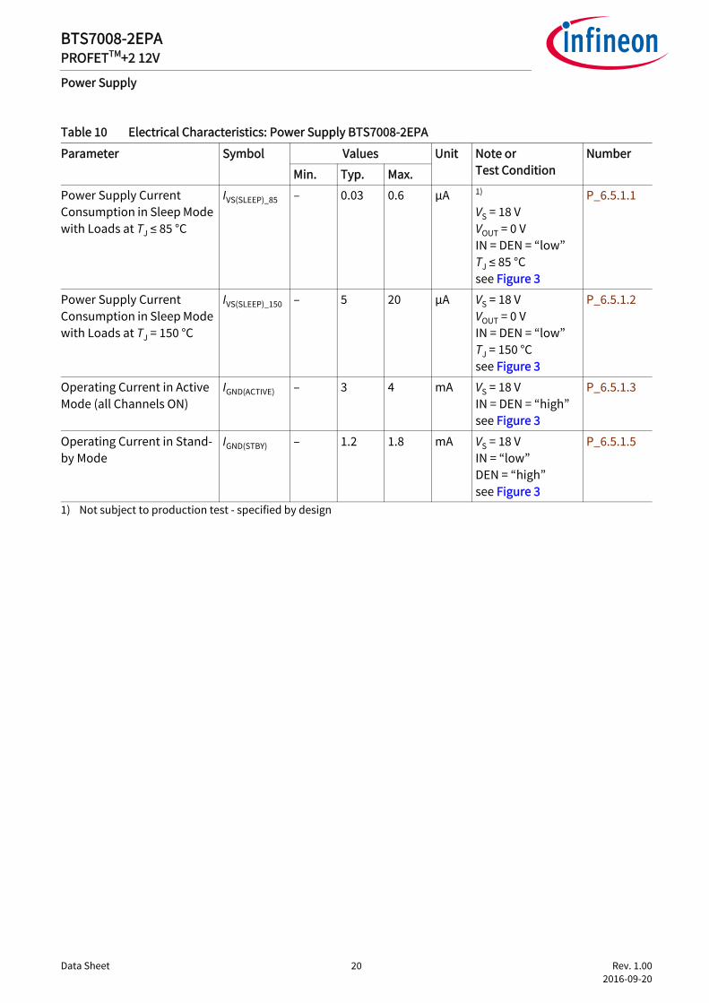
Table 10 Electrical Characteristics: Power Supply BTS7008-2EPA
Parameter Symbol Values Unit Note or Test Condition
Number
Min. Typ. Max.
Power Supply Current Consumption in Sleep Mode with Loads at TJ ≤ 85 °C
IVS(SLEEP)_85 – 0.03 0.6 µA 1)
VS = 18 VVOUT = 0 VIN = DEN = “low”TJ ≤ 85 °Csee Figure 3
1) Not subject to production test - specified by design
P_6.5.1.1
Power Supply Current Consumption in Sleep Mode with Loads at TJ = 150 °C
IVS(SLEEP)_150 – 5 20 µA VS = 18 VVOUT = 0 VIN = DEN = “low”TJ = 150 °Csee Figure 3
P_6.5.1.2
Operating Current in Active Mode (all Channels ON)
IGND(ACTIVE) – 3 4 mA VS = 18 VIN = DEN = “high”see Figure 3
P_6.5.1.3
Operating Current in Stand-by Mode
IGND(STBY) – 1.2 1.8 mA VS = 18 VIN = “low”DEN = “high”see Figure 3
P_6.5.1.5
Data Sheet 21 Rev. 1.00 2016-09-20
BTS7008-2EPAPROFETTM+2 12V
Power Stages
7 Power StagesThe high-side power stages are built using a N-channel vertical Power MOSFET with charge pump.
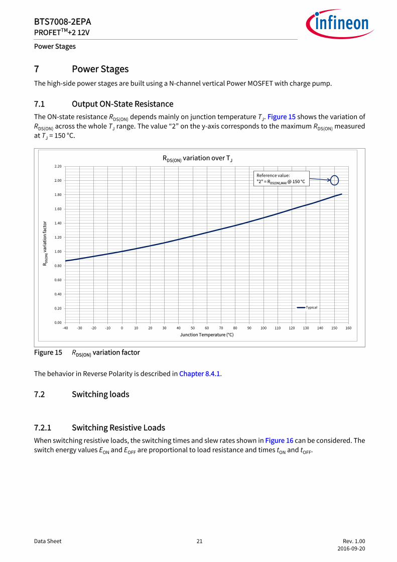
7.1 Output ON-State ResistanceThe ON-state resistance RDS(ON) depends mainly on junction temperature TJ. Figure 15 shows the variation ofRDS(ON) across the whole TJ range. The value “2” on the y-axis corresponds to the maximum RDS(ON) measuredat TJ = 150 °C.
Figure 15 RDS(ON) variation factor
The behavior in Reverse Polarity is described in Chapter 8.4.1.
7.2 Switching loads
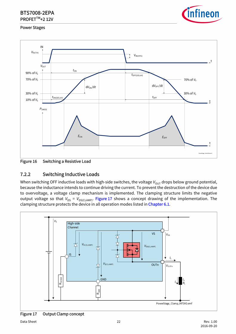
7.2.1 Switching Resistive LoadsWhen switching resistive loads, the switching times and slew rates shown in Figure 16 can be considered. Theswitch energy values EON and EOFF are proportional to load resistance and times tON and tOFF.
0.00
0.20
0.40
0.60
0.80
1.00
1.20
1.40
1.60
1.80
2.00
2.20
-40 -30 -20 -10 0 10 20 30 40 50 60 70 80 90 100 110 120 130 140 150 160
RD
S(O
N) v
aria
tio
n fa
cto
r
Junction Temperature (°C)
RDS(ON) variation over TJ
Typical
Reference value: "2" = RDS(ON),MAX @ 150 °C
Data Sheet 22 Rev. 1.00 2016-09-20
BTS7008-2EPAPROFETTM+2 12V
Power Stages
Figure 16 Switching a Resistive Load
7.2.2 Switching Inductive LoadsWhen switching OFF inductive loads with high-side switches, the voltage VOUT drops below ground potential,because the inductance intends to continue driving the current. To prevent the destruction of the device dueto overvoltage, a voltage clamp mechanism is implemented. The clamping structure limits the negativeoutput voltage so that VDS = VDS(CLAMP). Figure 17 shows a concept drawing of the implementation. Theclamping structure protects the device in all operation modes listed in Chapter 6.1.
Figure 17 Output Clamp concept
IN
tVOUT
VIN(TH)
dVON/dt
VIN(HYS)
PDMOS
t
t
PowerStage_SwitchRes.emf
EON EOFF
tON
tON(DELAY)
tOFF(DELAY)
dVOFF/dt
tOFF10% of VS
90% of VS
70% of VS
30% of VS 30% of VS
70% of VS
PowerStage_Clamp_INTDIO.emf
High-sideChannel
VS
L,RL
VO UTn
IL
VDS(CL AMP)
IL
VS
OUTn
VDS
GND
VS( CL AMP)
IS
VIS (CL AMP)
R SEN
SE
R GND
Data Sheet 23 Rev. 1.00 2016-09-20
BTS7008-2EPAPROFETTM+2 12V
Power Stages
During demagnetization of inductive loads, energy has to be dissipated in BTS7008-2EPA. The energy can becalculated with Equation (7.1):
(7.1)
The maximum energy, therefore the maximum inductance for a given current, is limited by the thermal designof the component. Please refer to Chapter 4.2 for the maximum allowed values of EAS (single pulse energy) andEAR (repetitive energy).
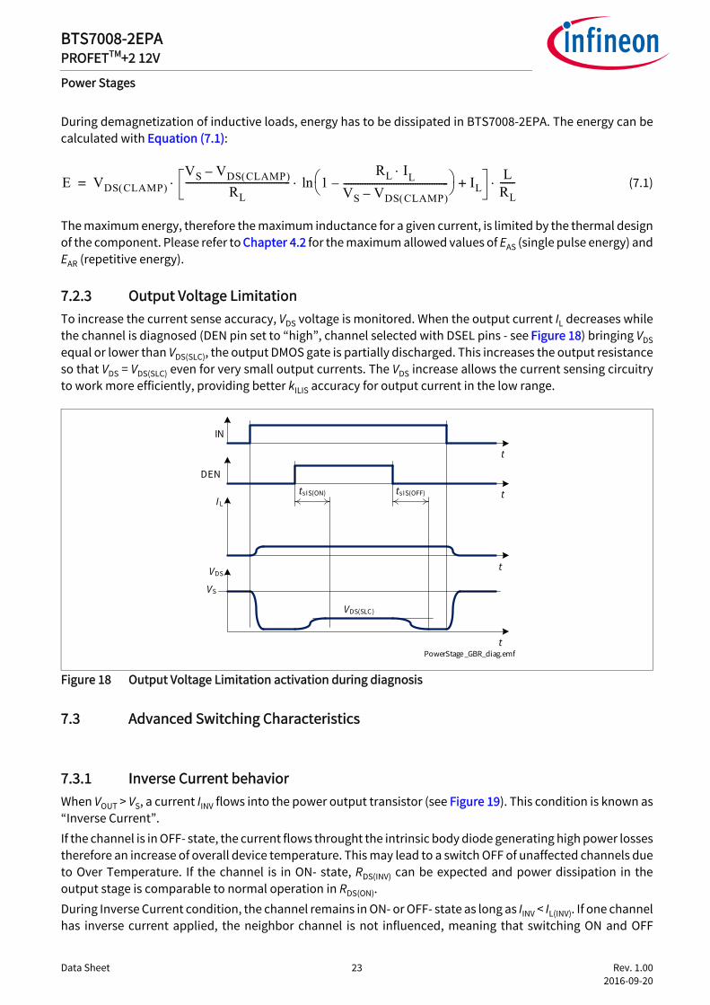
7.2.3 Output Voltage LimitationTo increase the current sense accuracy, VDS voltage is monitored. When the output current IL decreases whilethe channel is diagnosed (DEN pin set to “high”, channel selected with DSEL pins - see Figure 18) bringing VDSequal or lower than VDS(SLC), the output DMOS gate is partially discharged. This increases the output resistanceso that VDS = VDS(SLC) even for very small output currents. The VDS increase allows the current sensing circuitryto work more efficiently, providing better kILIS accuracy for output current in the low range.
Figure 18 Output Voltage Limitation activation during diagnosis
7.3 Advanced Switching Characteristics
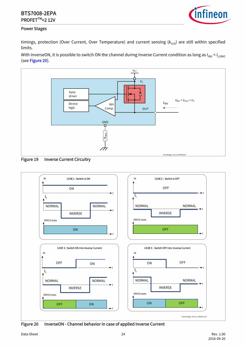
7.3.1 Inverse Current behaviorWhen VOUT > VS, a current IINV flows into the power output transistor (see Figure 19). This condition is known as“Inverse Current”.If the channel is in OFF- state, the current flows throught the intrinsic body diode generating high power lossestherefore an increase of overall device temperature. This may lead to a switch OFF of unaffected channels dueto Over Temperature. If the channel is in ON- state, RDS(INV) can be expected and power dissipation in theoutput stage is comparable to normal operation in RDS(ON).During Inverse Current condition, the channel remains in ON- or OFF- state as long as IINV < IL(INV). If one channelhas inverse current applied, the neighbor channel is not influenced, meaning that switching ON and OFF
E VDS CLAMP VS VDS CLAMP –
RL-------------------------------------------- 1
RL I L
VS VDS CLAMP –--------------------------------------------–
IL+ln LRL------ =
IN
IL
t
t
PowerStage_GBR_diag.emf
t
DENtsIS(ON) tsIS(OFF)
t
VDS
VDS(SLC)
VS
Data Sheet 24 Rev. 1.00 2016-09-20
BTS7008-2EPAPROFETTM+2 12V
Power Stages
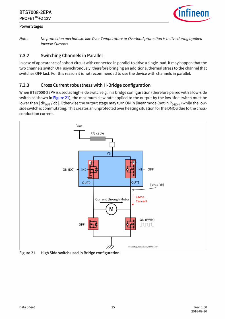
timings, protection (Over Current, Over Temperature) and current sensing (kILIS) are still within specifiedlimits. With InverseON, it is possible to switch ON the channel during Inverse Current condition as long as IINV < IL(INV)(see Figure 20).
Figure 19 Inverse Current Circuitry
Figure 20 InverseON - Channel behavior in case of applied Inverse Current
OUT
VS
VBAT
IINVINVComp.
VINV = VOUT > VS
Gate driver
Devicelogic
GND
PowerStage_InvCurr_INTDIO.emf
R GN
D
OFF
OFF
CASE 2 : Switch is OFFIN
tIL
t
DMOS state
t
INVERSE
NORMALNORMAL
ON
INVERSE
NORMAL
IL
t
DMOS state
tON
CASE 1 : Switch is ONIN
t
NORMAL
OFF
ON
CASE 4 : Switch OFF into Inverse Current
IN
tIL
t
DMOS state
t
INVERSE
NORMALNORMAL
ON
INVERSE
NORMAL
IL
t
DMOS state
tOFF
CASE 3 : Switch ON into Inverse Current
IN
t
NORMAL
OFF
ON
ON
OFF
PowerStage_InvCurr_INVON.emf
Data Sheet 25 Rev. 1.00 2016-09-20
BTS7008-2EPAPROFETTM+2 12V
Power Stages
Note: No protection mechanism like Over Temperature or Overload protection is active during applied Inverse Currents.
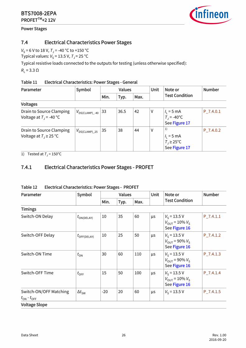
7.3.2 Switching Channels in ParallelIn case of appearance of a short circuit with connected in parallel to drive a single load, it may happen that thetwo channels switch OFF asynchronously, therefore bringing an additional thermal stress to the channel thatswitches OFF last. For this reason it is not recommended to use the device with channels in parallel.
7.3.3 Cross Current robustness with H-Bridge configurationWhen BTS7008-2EPA is used as high-side switch e.g. in a bridge configuration (therefore paired with a low-sideswitch as shown in Figure 21), the maximum slew rate applied to the output by the low-side switch must belower than | dVOUT / dt |. Otherwise the output stage may turn ON in linear mode (not in RDS(ON)) while the low-side switch is commutating. This creates an unprotected over heating situation for the DMOS due to the cross-conduction current.
Figure 21 High Side switch used in Bridge configuration
IN0 IN1
OUT0 OUT1
VS
PowerStage_PassiveSlew_PROFET.emf
T T
VBAT
R/L cable
M
ON (DC) OFF
ON (PWM)OFF
Current through MotorCross Current
| dVOUT / dt |
Data Sheet 26 Rev. 1.00 2016-09-20
BTS7008-2EPAPROFETTM+2 12V
Power Stages
7.4 Electrical Characteristics Power StagesVS = 6 V to 18 V, TJ = -40 °C to +150 °CTypical values: VS = 13.5 V, TJ = 25 °CTypical resistive loads connected to the outputs for testing (unless otherwise specified):RL = 3.3 Ω
7.4.1 Electrical Characteristics Power Stages - PROFET
Table 11 Electrical Characteristics: Power Stages - General
Parameter Symbol Values Unit Note or Test Condition
Number
Min. Typ. Max.
Voltages
Drain to Source Clamping Voltage at TJ = -40 °C
VDS(CLAMP)_-40 33 36.5 42 V IL = 5 mATJ = -40°CSee Figure 17
P_7.4.0.1
Drain to Source Clamping Voltage at TJ ≥ 25 °C
VDS(CLAMP)_25 35 38 44 V 1)
IL = 5 mATJ ≥ 25°CSee Figure 17
1) Tested at TJ = 150°C
P_7.4.0.2
Table 12 Electrical Characteristics: Power Stages - PROFET
Parameter Symbol Values Unit Note or Test Condition
Number
Min. Typ. Max.
Timings
Switch-ON Delay tON(DELAY) 10 35 60 μs VS = 13.5 VVOUT = 10% VSSee Figure 16
P_7.4.1.1
Switch-OFF Delay tOFF(DELAY) 10 25 50 μs VS = 13.5 VVOUT = 90% VSSee Figure 16
P_7.4.1.2
Switch-ON Time tON 30 60 110 μs VS = 13.5 VVOUT = 90% VSSee Figure 16
P_7.4.1.3
Switch-OFF Time tOFF 15 50 100 μs VS = 13.5 VVOUT = 10% VSSee Figure 16
P_7.4.1.4
Switch-ON/OFF MatchingtON - tOFF
ΔtSW -20 20 60 μs VS = 13.5 V P_7.4.1.5
Voltage Slope
Data Sheet 27 Rev. 1.00 2016-09-20
BTS7008-2EPAPROFETTM+2 12V
Power Stages
7.5 Electrical Characteristics - Power Output Stages
7.5.1 Power Output Stage - 8 mΩ
Switch-ON Slew Rate (dV/dt)ON 0.3 0.6 0.9 V/μs VS = 13.5 VVOUT = 30% to 70% of VSSee Figure 16
P_7.4.1.6
Switch-OFF Slew Rate -(dV/dt)OFF 0.3 0.6 0.9 V/μs VS = 13.5 VVOUT = 70% to 30% of VSSee Figure 16
P_7.4.1.7
Slew Rate Matching(dV/dt)ON - (dV/dt)OFF
Δ(dV/dt)SW -0.15 0 0.15 V/μs VS = 13.5 V P_7.4.1.8
Voltages
Output Voltage Drop Limitation at Small Load Currents
VDS(SLC) 2 7 18 mV 1)
DEN = “high”channel selected with DSEL pinIL = IL(OL) = 20 mASee Figure 18
P_7.4.1.9
1) Not subject to production test - specified by design
Table 13 Electrical Characteristics: Power Stages - 8 mΩ
Parameter Symbol Values Unit Note or Test Condition
Number
Min. Typ. Max.
Output characteristics
ON-State Resistance at TJ = 25 °C
RDS(ON)_25 – 9 – mΩ 1)
TJ = 25 °CP_7.5.1.1
ON-State Resistance at TJ = 150 °C
RDS(ON)_150 – – 16 mΩ TJ = 150 °C P_7.5.1.2
ON-State Resistance in Cranking
RDS(ON)_CRAN
K
– – 20 mΩ TJ = 150 °CVS = 3.1 VIL = 2 A
P_7.5.1.3
ON-State Resistance in Inverse Current at TJ = 25 °C
RDS(INV)_25 – 10 – mΩ 1)
TJ = 25 °CVS = 13.5 VIL = -4 Asee Figure 19
P_7.5.1.4
Table 12 Electrical Characteristics: Power Stages - PROFET (continued)
Parameter Symbol Values Unit Note or Test Condition
Number
Min. Typ. Max.
Data Sheet 28 Rev. 1.00 2016-09-20
BTS7008-2EPAPROFETTM+2 12V
Power Stages
ON-State Resistance in Inverse Current at TJ = 150 °C
RDS(INV)_150 – – 20 mΩ TJ = 150 °CVS = 13.5 VIL = -4 Asee Figure 19
P_7.5.1.5
ON-State Resistance in Reverse Polarity at TJ = 25 °C
RDS(REV)_25 – 10 – mΩ 1)
TJ = 25 °CVS = -13.5 VIL = -4 A
P_7.5.1.6
ON-State Resistance in Reverse Polarity at TJ = 150 °C
RDS(REV)_150 – – 22 mΩ TJ = 150 °CVS = -13.5 VIL = -4 A
P_7.5.1.7
Nominal Load Current per Channel (all Channels Active)
IL(NOM) – 7.5 – A 1)
TA = 85 °CTJ ≤ 150 °C
P_7.5.1.8
Output Leakage Current at TJ ≤ 85 °C
IL(OFF)_85 – 0.01 0.5 μA 1)
VOUT = 0 VIN = “low”TA ≤ 85 °C
P_7.5.1.9
Output Leakage Current at TJ = 150 °C
IL(OFF)_150 – 2.5 8 μA VOUT = 0 VIN = “low”TA = 150 °C
P_7.5.1.10
Inverse Current Capability IL(INV) – 7.5 – A 1)
VS < VOUTIN = “high”see Figure 19
P_7.5.1.11
Voltage Slope
Passive Slew Rate (e.g. for Half Bridge Configuration)
|dVOUT / dt | – – 10 V/μs 1)
VS = 13.5 Vsee Figure 21
P_7.5.1.12
Voltages
Drain Source Diode Voltage |VDS(DIODE)| – 550 700 mV IL = -190 mATJ = 150 °C
P_7.5.1.13
Switching Energy
Switch-ON Energy EON – 0.24 – mJ 1)
VS = 18 Vsee Figure 16
P_7.5.1.14
Switch-OFF Energy EOFF – 0.32 – mJ 1)
VS = 18 Vsee Figure 16
P_7.5.1.15
1) Not subject to production test - specified by design
Table 13 Electrical Characteristics: Power Stages - 8 mΩ (continued)
Parameter Symbol Values Unit Note or Test Condition
Number
Min. Typ. Max.
Data Sheet 29 Rev. 1.00 2016-09-20
BTS7008-2EPAPROFETTM+2 12V
Protection
8 ProtectionThe BTS7008-2EPA is protected against Over Temperature, Overload, Reverse Battery (with ReverSave™) andOver voltage. Over Temperature and Overload protections are working when the device is not in Sleep mode.Over Voltage protection works in all operation modes. Reverse Battery protection works when the GND andVS pins are reverse supplied.
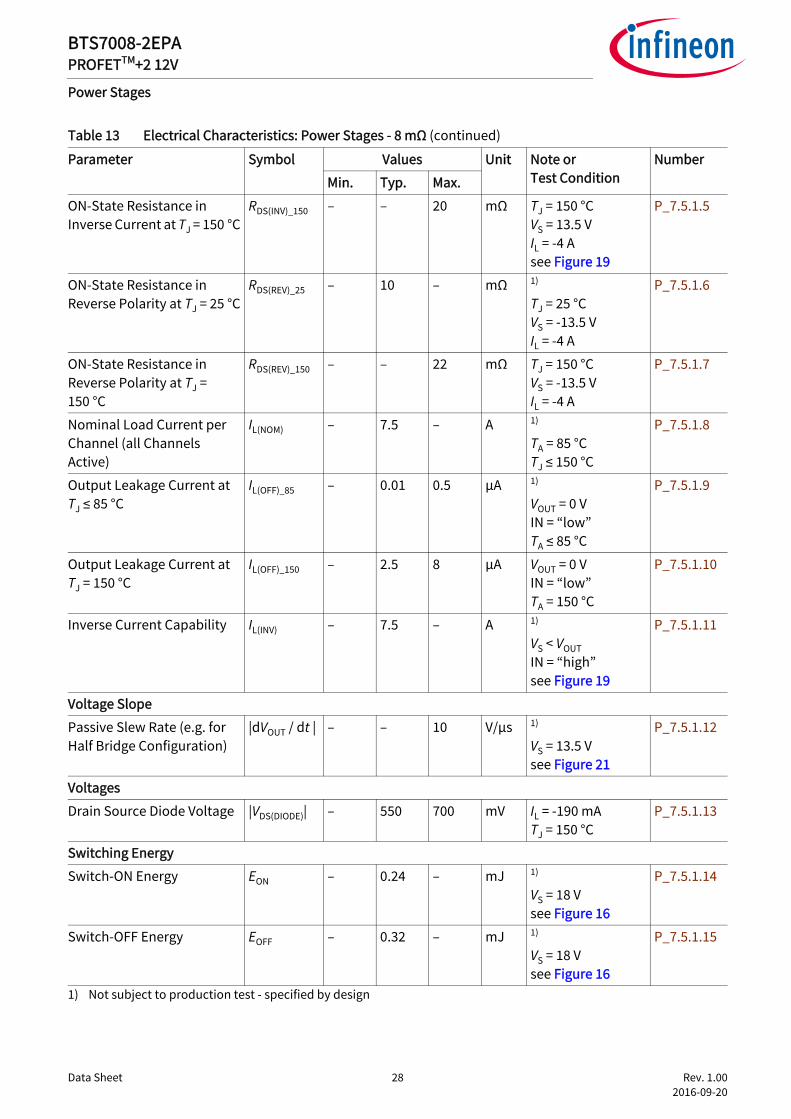
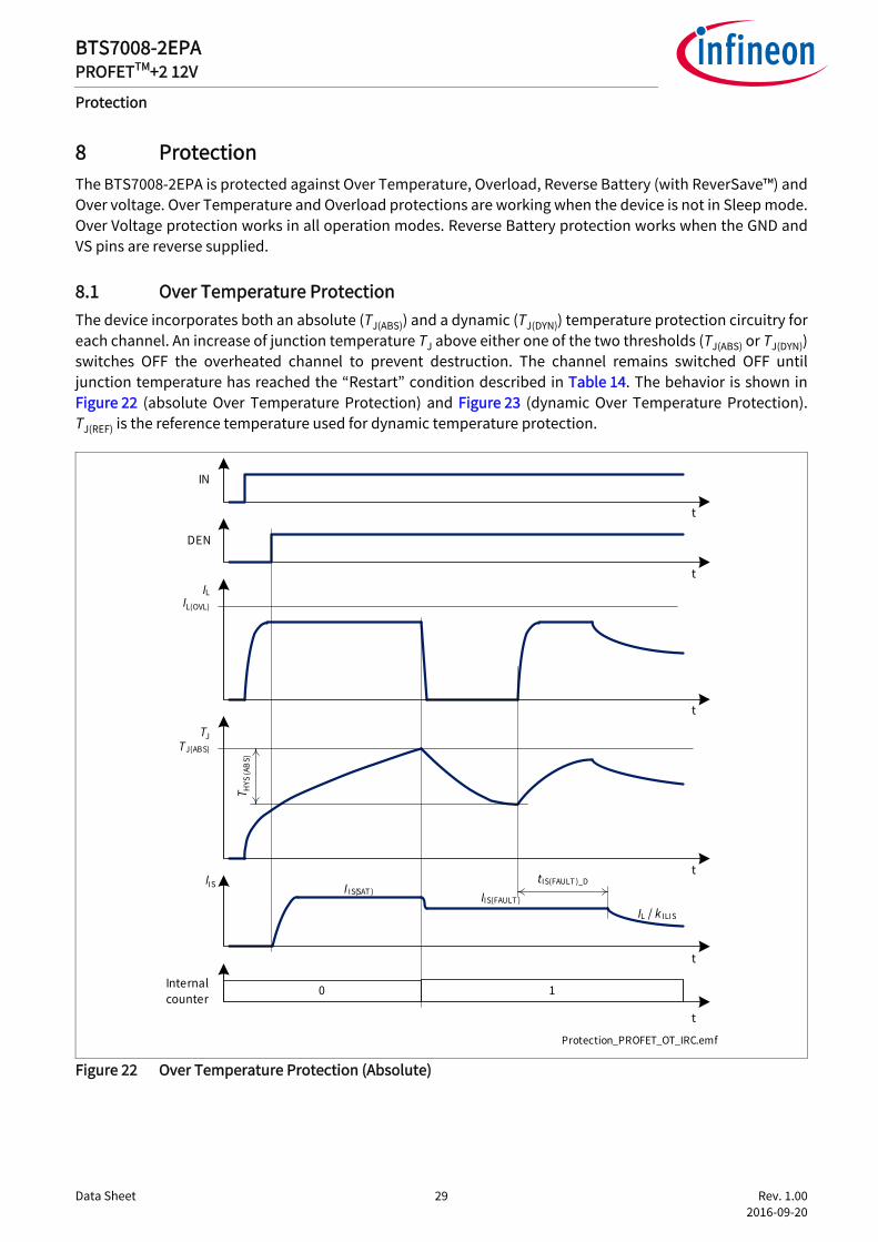
8.1 Over Temperature ProtectionThe device incorporates both an absolute (TJ(ABS)) and a dynamic (TJ(DYN)) temperature protection circuitry foreach channel. An increase of junction temperature TJ above either one of the two thresholds (TJ(ABS) or TJ(DYN))switches OFF the overheated channel to prevent destruction. The channel remains switched OFF untiljunction temperature has reached the “Restart” condition described in Table 14. The behavior is shown inFigure 22 (absolute Over Temperature Protection) and Figure 23 (dynamic Over Temperature Protection).TJ(REF) is the reference temperature used for dynamic temperature protection.
Figure 22 Over Temperature Protection (Absolute)
IL(OVL)
IL
t
TJ
IIS
Protection_PROFET_OT_IRC.emf
DEN
Internal counter
TJ(ABS)
t
t
t
t
10
IN
t
I IS(SAT ) IIS(FAULT )
T HYS
(AB
S)
tIS(FAULT )_D
IL / k ILIS
Data Sheet 30 Rev. 1.00 2016-09-20
BTS7008-2EPAPROFETTM+2 12V
Protection
Figure 23 Over Temperature Protection (Dynamic)
When the Over Temperature protection circuitry allows the channel to be switched ON again, the retrystrategy described in Chapter 8.3 is followed.
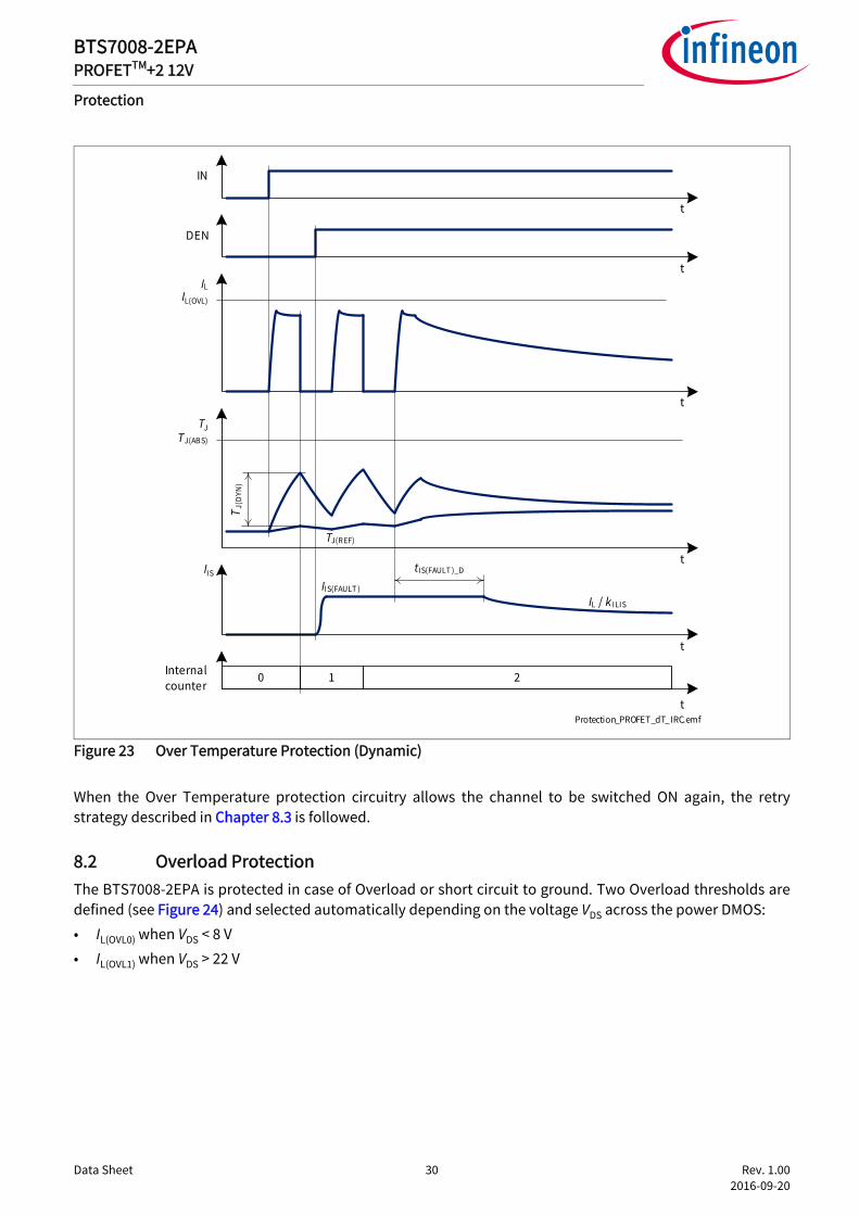
8.2 Overload ProtectionThe BTS7008-2EPA is protected in case of Overload or short circuit to ground. Two Overload thresholds aredefined (see Figure 24) and selected automatically depending on the voltage VDS across the power DMOS:• IL(OVL0) when VDS < 8 V• IL(OVL1) when VDS > 22 V
IL(OVL)
IL
t
TJ
IIS
Protection_PROFET_dT_IRC.emf
DEN
Internal counter
TJ(ABS)
t
t
t
t
10
IN
t
IIS(FAULT )
T J(D
YN)
tIS(FAULT )_D
IL / k ILIS
TJ(REF)
2
Data Sheet 31 Rev. 1.00 2016-09-20
BTS7008-2EPAPROFETTM+2 12V
Protection
Figure 24 Overload Current Thresholds variation with VDS
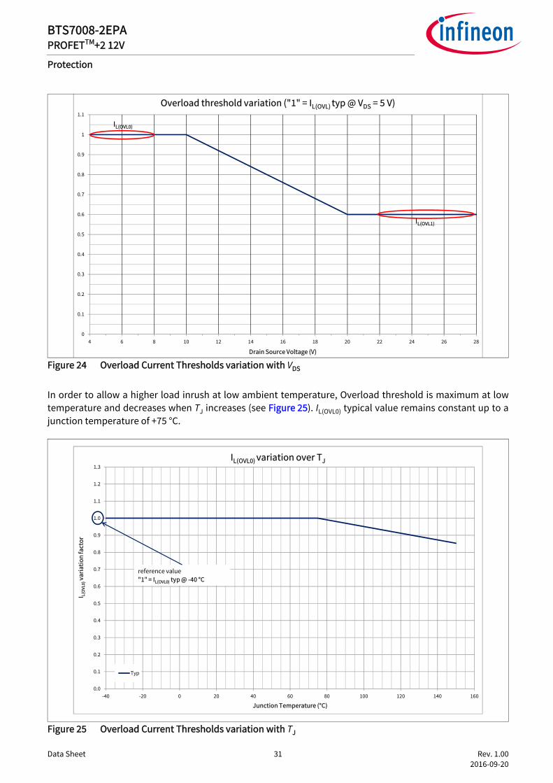
In order to allow a higher load inrush at low ambient temperature, Overload threshold is maximum at lowtemperature and decreases when TJ increases (see Figure 25). IL(OVL0) typical value remains constant up to ajunction temperature of +75 °C.
Figure 25 Overload Current Thresholds variation with TJ
0
0.1
0.2
0.3
0.4
0.5
0.6
0.7
0.8
0.9
1
1.1
4 6 8 10 12 14 16 18 20 22 24 26 28
Drain Source Voltage (V)
Overload threshold variation ("1" = IL(OVL) typ @ VDS = 5 V)
IL(OVL0)
IL(OVL1)
0.0
0.1
0.2
0.3
0.4
0.5
0.6
0.7
0.8
0.9
1.0
1.1
1.2
1.3
-40 -20 0 20 40 60 80 100 120 140 160
I L(O
VL0
)va
riat
ion
fact
or
Junction Temperature (°C)
IL(OVL0) variation over TJ
Typ
reference value"1" = IL(OVL0) typ @ -40 °C
Data Sheet 32 Rev. 1.00 2016-09-20
BTS7008-2EPAPROFETTM+2 12V
Protection
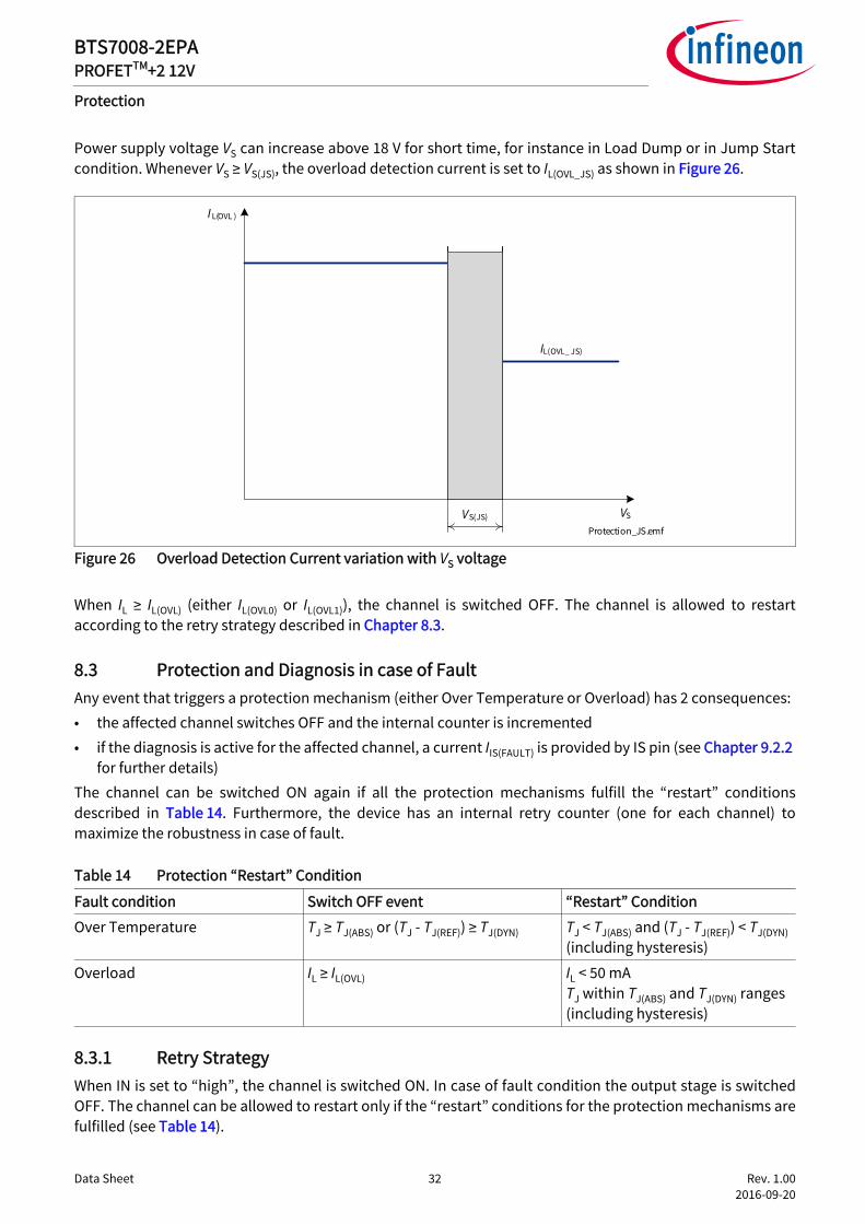
Power supply voltage VS can increase above 18 V for short time, for instance in Load Dump or in Jump Startcondition. Whenever VS ≥ VS(JS), the overload detection current is set to IL(OVL_JS) as shown in Figure 26.
Figure 26 Overload Detection Current variation with VS voltage
When IL ≥ IL(OVL) (either IL(OVL0) or IL(OVL1)), the channel is switched OFF. The channel is allowed to restartaccording to the retry strategy described in Chapter 8.3.
8.3 Protection and Diagnosis in case of FaultAny event that triggers a protection mechanism (either Over Temperature or Overload) has 2 consequences:• the affected channel switches OFF and the internal counter is incremented• if the diagnosis is active for the affected channel, a current IIS(FAULT) is provided by IS pin (see Chapter 9.2.2
for further details)The channel can be switched ON again if all the protection mechanisms fulfill the “restart” conditionsdescribed in Table 14. Furthermore, the device has an internal retry counter (one for each channel) tomaximize the robustness in case of fault.
8.3.1 Retry StrategyWhen IN is set to “high”, the channel is switched ON. In case of fault condition the output stage is switchedOFF. The channel can be allowed to restart only if the “restart” conditions for the protection mechanisms arefulfilled (see Table 14).
Table 14 Protection “Restart” Condition
Fault condition Switch OFF event “Restart” Condition
Over Temperature TJ ≥ TJ(ABS) or (TJ - TJ(REF)) ≥ TJ(DYN) TJ < TJ(ABS) and (TJ - TJ(REF)) < TJ(DYN) (including hysteresis)
Overload IL ≥ IL(OVL) IL < 50 mATJ within TJ(ABS) and TJ(DYN) ranges (including hysteresis)
Protection_JS.emf
I L(OVL )
VSVS(JS)
IL(OVL_ JS)
Data Sheet 33 Rev. 1.00 2016-09-20
BTS7008-2EPAPROFETTM+2 12V
Protection
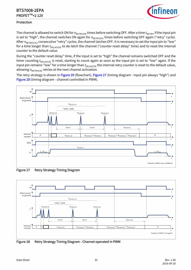
The channel is allowed to switch ON for nRETRY(CR) times before switching OFF. After a time tRETRY, if the input pinis set to “high”, the channel switches ON again for nRETRY(NT) times before switching OFF again (“retry” cycle).After nRETRY(CYC) consecutive “retry” cycles, the channel latches OFF. It is necessary to set the input pin to “low”for a time longer than tDELAY(CR) to de-latch the channel (“counter reset delay” time) and to reset the internalcounter to the default value.During the “counter reset delay” time, if the input is set to “high” the channel remains switched OFF and thetimer counting tDELAY(CR) is reset, starting to count again as soon as the input pin is set to “low” again. If theinput pin remains “low” for a time longer than tDELAY(CR) the internal retry counter is reset to the default value,allowing nRETRY(CR) retries at the next channel activation.The retry strategy is shown in Figure 29 (flowchart), Figure 27 (timing diagram - input pin always “high”) andFigure 28 (timing diagram - channel controlled in PWM).
Figure 27 Retry Strategy Timing Diagram
Figure 28 Retry Strategy Timing Diagram - Channel operated in PWM
t
IN
tR ETR Y
Short circuit to ground
IL
0 1 nRETR Y(C R)Internal counter
nRETRY(CR) + nR ETR Y(NT ) nR ETR Y(C R) + (n R ETR Y(C YC) * nR ETR Y(NT ))
tDELAY(CR)tR ETR Y
0
nR ETR Y(C R) nR ETR Y(NT)
"retry" cycle
nRETR Y(NT)
t
t
t
Protection_PROFET_time_noPWM.emf
nRETRY(CYC)
t
DEN
t
IIS
IIS(FAULT )
IL / kILISIL / k ILIS
t
IN
tR ETR Y
Short circuit to ground
IL
0 1 nR ETR Y(C R)Internal counter
n RETRY(CR) + nR ETR Y(NT ) nRETRY(CR) + (nRETRY(CYC) * nRETRY(NT))
tDELAY(C R)tR ETR Y
0
nR ETRY(CR) nR ETR Y(NT)
"retry" cycle
nR ETR Y(NT)
t
t
tProtection_PROFET_Timings.emf
nRETRY(CYC)
Data Sheet 34 Rev. 1.00 2016-09-20
BTS7008-2EPAPROFETTM+2 12V
Protection
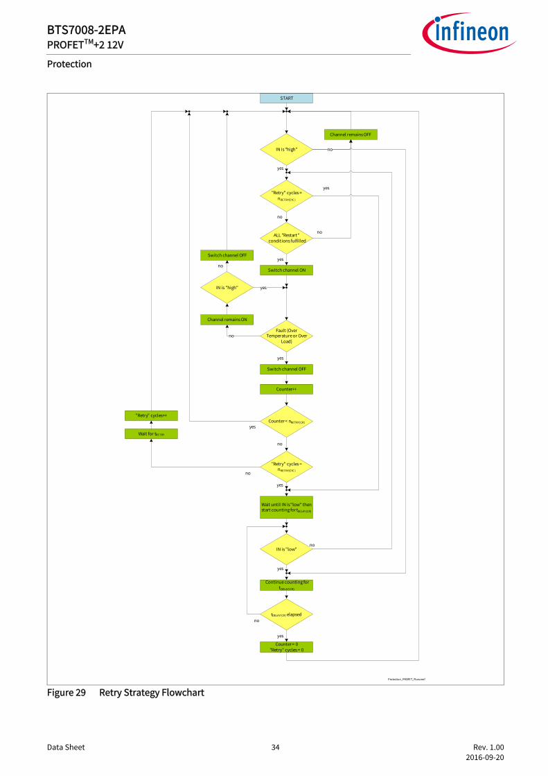
Figure 29 Retry Strategy FlowchartProtection_PROFET_Flow.emf
Fault (Over Temperature or Over
Load)
Switch channel ON
no
Channel remains ON
Switch channel OFF
yes
Counter++
IN is "high"
yes
Channel remains OFF
yes
"Retry" cycles = nRETRY(CYC )
no
Wait for tRETRY
"Retry" cycles++
yes
Wait until IN is "low" then start counting for tDELAY (CR)
IN is "low"
tDELAY(CR) elapsed
Continue counting for tDELAY( CR)
yes
no
no
yes
Counter = 0"Retry" cycles = 0
Counter < nRETRY( CR)
no
"Retry" cycles = nRETRY(CYC )
yes
yes
IN is "high" yes
Switch channel OFF
no
START
no
ALL "Restart "conditions fulfilled
no
no
Data Sheet 35 Rev. 1.00 2016-09-20
BTS7008-2EPAPROFETTM+2 12V
Protection
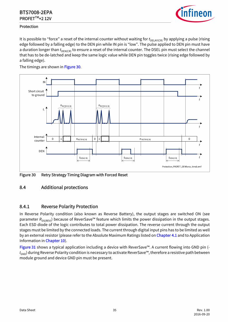
It is possible to “force” a reset of the internal counter without waiting for tDELAY(CR) by applying a pulse (risingedge followed by a falling edge) to the DEN pin while IN pin is “low”. The pulse applied to DEN pin must havea duration longer than tDEN(CR) to ensure a reset of the internal counter. The DSEL pin must select the channelthat has to be de-latched and keep the same logic value while DEN pin toggles twice (rising edge followed bya falling edge).The timings are shown in Figure 30.
Figure 30 Retry Strategy Timing Diagram with Forced Reset
8.4 Additional protections
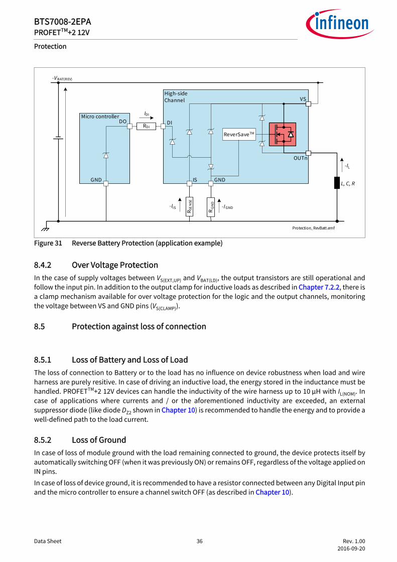
8.4.1 Reverse Polarity ProtectionIn Reverse Polarity condition (also known as Reverse Battery), the output stages are switched ON (seeparameter RDS(REV)) because of ReverSave™ feature which limits the power dissipation in the output stages.Each ESD diode of the logic contributes to total power dissipation. The reverse current through the outputstages must be limited by the connected loads. The current through digital input pins has to be limited as wellby an external resistor (please refer to the Absolute Maximum Ratings listed on Chapter 4.1 and to ApplicationInformation in Chapter 10).Figure 31 shows a typical application including a device with ReverSave™. A current flowing into GND pin (-IGND) during Reverse Polarity condition is necessary to activate ReverSave™, therefore a resistive path betweenmodule ground and device GND pin must be present.
t
IN
Short circuit to ground
IL
0 1Internal counter
nR ETR Y(CR)
t
t
t
Protection_PROFET_DENforce_time2.emf
DEN
nR ETRY(CR)
1
ttDEN(CR)
0
tDEN(CR)
nR ETR Y(C R)
tDEN(CR)
n RETR Y(CR) 0
Data Sheet 36 Rev. 1.00 2016-09-20
BTS7008-2EPAPROFETTM+2 12V
Protection
Figure 31 Reverse Battery Protection (application example)
8.4.2 Over Voltage ProtectionIn the case of supply voltages between VS(EXT,UP) and VBAT(LD), the output transistors are still operational andfollow the input pin. In addition to the output clamp for inductive loads as described in Chapter 7.2.2, there isa clamp mechanism available for over voltage protection for the logic and the output channels, monitoringthe voltage between VS and GND pins (VS(CLAMP)).
8.5 Protection against loss of connection
8.5.1 Loss of Battery and Loss of LoadThe loss of connection to Battery or to the load has no influence on device robustness when load and wireharness are purely resitive. In case of driving an inductive load, the energy stored in the inductance must behandled. PROFETTM+2 12V devices can handle the inductivity of the wire harness up to 10 µH with IL(NOM). Incase of applications where currents and / or the aforementioned inductivity are exceeded, an externalsuppressor diode (like diode DZ2 shown in Chapter 10) is recommended to handle the energy and to provide awell-defined path to the load current.
8.5.2 Loss of GroundIn case of loss of module ground with the load remaining connected to ground, the device protects itself byautomatically switching OFF (when it was previously ON) or remains OFF, regardless of the voltage applied onIN pins.In case of loss of device ground, it is recommended to have a resistor connected between any Digital Input pinand the micro controller to ensure a channel switch OFF (as described in Chapter 10).
Protection_RevBatt.emf
High-sideChannel
L, C, R
VS
OUTn
GNDISR S
EN
SE
RG
ND
ReverSaveTM
DIMicro controller
DORDI
GND
-IL
-IGND-IIS
IDI
-VBAT(REV)
Data Sheet 37 Rev. 1.00 2016-09-20
BTS7008-2EPAPROFETTM+2 12V
Protection
8.6 Electrical Characteristics ProtectionVS = 6 V to 18 V, TJ = -40 °C to +150 °CTypical values: VS = 13.5 V, TJ = 25 °CTypical resistive loads connected to the outputs for testing (unless otherwise specified):RL = 3.3 Ω
8.6.1 Electrical Characteristics Protection
Table 15 Electrical Characteristics: Protection - General
Parameter Symbol Values Unit Note or Test Condition
Number
Min. Typ. Max.
Thermal Shutdown Temperature (Absolute)
TJ(ABS) 150 175 220 °C 1)2)
See Figure 22
1) Functional test only2) Tested at TJ = 150°C only
P_8.6.0.1
Thermal Shutdown Hysteresis (Absolute)
THYS(ABS) – 30 – K 3)
See Figure 22
3) Not subject to production test - specified by design
P_8.6.0.2
Thermal Shutdown Temperature (Dynamic)
TJ(DYN) – 80 – K 3)
See Figure 23P_8.6.0.3
Power Supply Clamping Voltage at TJ = -40 °C
VS(CLAMP)_-40 33 36.5 42 V IVS = 5 mATJ = -40 °CSee Figure 17
P_8.6.0.6
Power Supply Clamping Voltage at TJ ≥ 25 °C
VS(CLAMP)_25 35 38 44 V 2)
IVS = 5 mATJ ≥ 25 °CSee Figure 17
P_8.6.0.7
Power Supply Voltage Threshold for Over Current Threshold Reduction in case of Short Circuit
VS(JS) 20.5 22.5 24.5 V 3)
Setup acc. to AEC-Q100-012
P_8.6.0.8
Table 16 Electrical Characteristics: Protection
Parameter Symbol Values Unit Note or Test Condition
Number
Min. Typ. Max.
Automatic Retries in Case of Fault after a Counter Reset
nRETRY(CR) – 5 – 1)
See Figure 27 and Figure 28
P_8.6.1.1
Automatic Retries in Case of Fault after the First tRETRY Activation
nRETRY(NT) – 1 – 1)
See Figure 27 and Figure 28
P_8.6.1.3
Maximum “Retry” Cycles allowed before Channel Latch OFF
nRETRY(CYC) – 2 – 1)
See Figure 27 and Figure 28
P_8.6.1.4
Data Sheet 38 Rev. 1.00 2016-09-20
BTS7008-2EPAPROFETTM+2 12V
Protection
8.7 Electrical Characteristics Protection - Power Output Stages
8.7.1 Protection Power Output Stage - 8 mΩ
Auto Retry Time after Fault Condition
tRETRY 40 70 100 ms 1)
See Figure 27 and Figure 28
P_8.6.1.5
Counter Reset Delay Time after Fault Condition
tDELAY(CR) 40 70 100 ms 1)
See Figure 27 and Figure 28
P_8.6.1.6
Minimum DEN Pulse Duration for Counter Reset
tDEN(CR) 50 100 150 µs 2)
See Figure 30P_8.6.1.7
1) Functional test only2) Not subject to production test - specified by design
Table 17 Electrical Characteristics: Protection - 8 mΩ
Parameter Symbol Values Unit Note or Test Condition
Number
Min. Typ. Max.
Overload Detection Current at TJ = -40 °C
IL(OVL0)_-40 77 88 99 A 1)
TJ = -40 °CdI/dt = 0.4 A/µssee Figure 24
1) Functional test only
P_8.7.1.1
Overload Detection Current at TJ = 25 °C
IL(OVL0)_25 77 88 99 A 2)
TJ = 25 °CdI/dt = 0.4 A/µssee Figure 24
2) Not subject to production test - specified by design
P_8.7.1.7
Overload Detection Current at TJ = 150 °C
IL(OVL0)_150 65 75 85 A 2)
TJ = 150 °CdI/dt = 0.4 A/µssee Figure 24
P_8.7.1.8
Overload Detection Current at High VDS
IL(OVL1) – 54 – A 2)
dI/dt = 0.4 A/µssee Figure 24
P_8.7.1.5
Overload Detection CurrentJump Start Condition
IL(OVL_JS) – 54 – A 2)
VS > VS(JS)dI/dt = 0.4 A/µssee Figure 26
P_8.7.1.6
Table 16 Electrical Characteristics: Protection (continued)
Parameter Symbol Values Unit Note or Test Condition
Number
Min. Typ. Max.
Data Sheet 39 Rev. 1.00 2016-09-20
BTS7008-2EPAPROFETTM+2 12V
Diagnosis
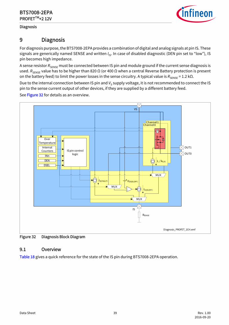
9 DiagnosisFor diagnosis purpose, the BTS7008-2EPA provides a combination of digital and analog signals at pin IS. Thesesignals are generically named SENSE and written IIS. In case of disabled diagnostic (DEN pin set to “low”), ISpin becomes high impedance.A sense resistor RSENSE must be connected between IS pin and module ground if the current sense diagnosis isused. RSENSE value has to be higher than 820 Ω (or 400 Ω when a central Reverse Battery protection is presenton the battery feed) to limit the power losses in the sense circuitry. A typical value is RSENSE = 1.2 kΩ.Due to the internal connection between IS pin and VS supply voltage, it is not recommended to connect the ISpin to the sense current output of other devices, if they are supplied by a different battery feed.See Figure 32 for details as an overview.
Figure 32 Diagnosis Block Diagram
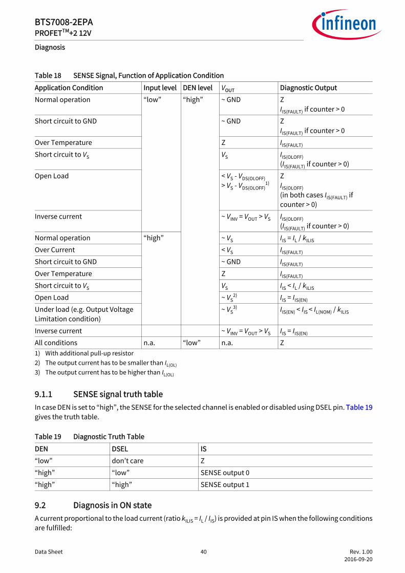
9.1 Overview Table 18 gives a quick reference for the state of the IS pin during BTS7008-2EPA operation.
Channel 1
Diagnosis_PROFET_2CH.emf
IS pin control logic
Internal Counters
INn
DSEL
DEN
Over Temperature
IIS(FAULT)
OUT0
VS
MUX
VDS(OLOFF )
IIS(OLOFF )
MUX
IS
RSENSE
OUT1
MUX
+
Channel 0
T
IL / kILIS
Data Sheet 40 Rev. 1.00 2016-09-20
BTS7008-2EPAPROFETTM+2 12V
Diagnosis
9.1.1 SENSE signal truth tableIn case DEN is set to “high”, the SENSE for the selected channel is enabled or disabled using DSEL pin. Table 19gives the truth table.
9.2 Diagnosis in ON stateA current proportional to the load current (ratio kILIS = IL / IIS) is provided at pin IS when the following conditionsare fulfilled:
Table 18 SENSE Signal, Function of Application Condition
Application Condition Input level DEN level VOUT Diagnostic Output
Normal operation “low” “high” ~ GND ZIIS(FAULT) if counter > 0
Short circuit to GND ~ GND ZIIS(FAULT) if counter > 0
Over Temperature Z IIS(FAULT)
Short circuit to VS VS IIS(OLOFF)(IIS(FAULT) if counter > 0)
Open Load < VS - VDS(OLOFF) > VS - VDS(OLOFF)
1)
1) With additional pull-up resistor
Z IIS(OLOFF) (in both cases IIS(FAULT) if counter > 0)
Inverse current ~ VINV = VOUT > VS IIS(OLOFF)(IIS(FAULT) if counter > 0)
Normal operation “high” ~ VS IIS = IL / kILIS
Over Current < VS IIS(FAULT)
Short circuit to GND ~ GND IIS(FAULT)
Over Temperature Z IIS(FAULT)
Short circuit to VS VS IIS < IL / kILIS
Open Load ~ VS2)
2) The output current has to be smaller than IL(OL)
IIS = IIS(EN)
Under load (e.g. Output Voltage Limitation condition)
~ VS3)
3) The output current has to be higher than IL(OL)
IIS(EN) < IIS < IL(NOM) / kILIS
Inverse current ~ VINV = VOUT > VS IIS = IIS(EN)
All conditions n.a. “low” n.a. Z
Table 19 Diagnostic Truth Table
DEN DSEL IS
“low” don’t care Z
“high” “low” SENSE output 0
“high” “high” SENSE output 1
Data Sheet 41 Rev. 1.00 2016-09-20
BTS7008-2EPAPROFETTM+2 12V
Diagnosis
• the power output stage is switched ON with VDS < 2 V• the diagnosis is enabled for that channel• no fault (as described in Chapter 8.3) is present or was present and not cleared yet (see Chapter 9.2.2 for
further details)If a “hard” failure mode is present or was present and not cleared yet a current IIS(FAULT) is provided at IS pin .
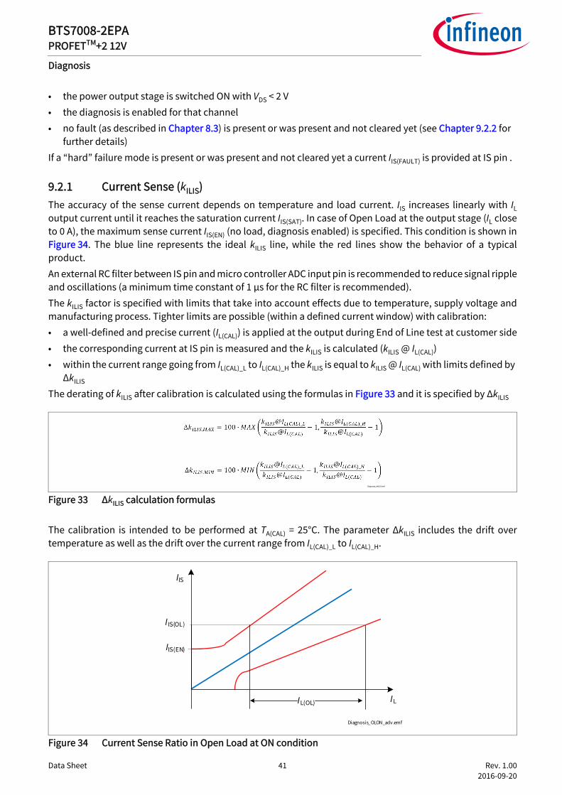
9.2.1 Current Sense (kILIS)The accuracy of the sense current depends on temperature and load current. IIS increases linearly with ILoutput current until it reaches the saturation current IIS(SAT). In case of Open Load at the output stage (IL closeto 0 A), the maximum sense current IIS(EN) (no load, diagnosis enabled) is specified. This condition is shown inFigure 34. The blue line represents the ideal kILIS line, while the red lines show the behavior of a typicalproduct.An external RC filter between IS pin and micro controller ADC input pin is recommended to reduce signal rippleand oscillations (a minimum time constant of 1 µs for the RC filter is recommended).The kILIS factor is specified with limits that take into account effects due to temperature, supply voltage andmanufacturing process. Tighter limits are possible (within a defined current window) with calibration:• a well-defined and precise current (IL(CAL)) is applied at the output during End of Line test at customer side• the corresponding current at IS pin is measured and the kILIS is calculated (kILIS @ IL(CAL))• within the current range going from IL(CAL)_L to IL(CAL)_H the kILIS is equal to kILIS @ IL(CAL) with limits defined by
ΔkILIS
The derating of kILIS after calibration is calculated using the formulas in Figure 33 and it is specified by ΔkILIS
Figure 33 ΔkILIS calculation formulas
The calibration is intended to be performed at TA(CAL) = 25°C. The parameter ΔkILIS includes the drift overtemperature as well as the drift over the current range from IL(CAL)_L to IL(CAL)_H.
Figure 34 Current Sense Ratio in Open Load at ON condition
Diagnosis_dKILIS.emf
IIS
ILIL(OL)
IIS(OL)
Diagnosis_OLON_adv .emf
IIS(EN)
Data Sheet 42 Rev. 1.00 2016-09-20
BTS7008-2EPAPROFETTM+2 12V
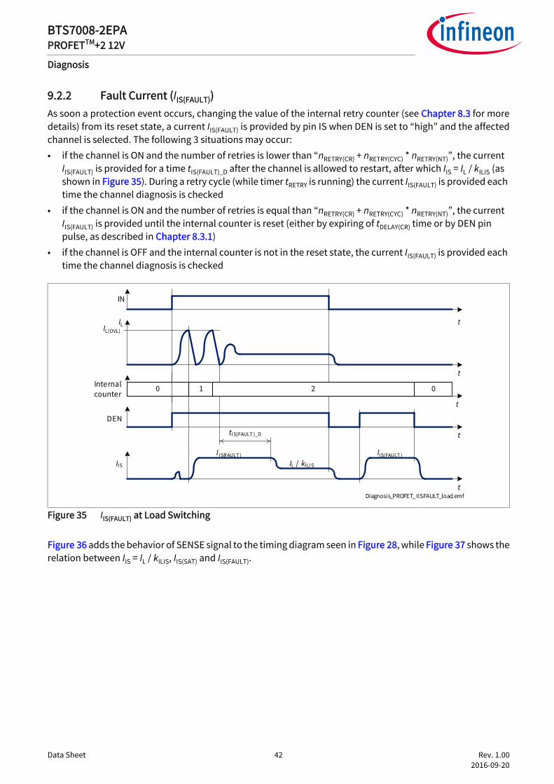
Diagnosis
9.2.2 Fault Current (IIS(FAULT))As soon a protection event occurs, changing the value of the internal retry counter (see Chapter 8.3 for moredetails) from its reset state, a current IIS(FAULT) is provided by pin IS when DEN is set to “high” and the affectedchannel is selected. The following 3 situations may occur:• if the channel is ON and the number of retries is lower than “nRETRY(CR) + nRETRY(CYC) * nRETRY(NT)”, the current
IIS(FAULT) is provided for a time tIS(FAULT)_D after the channel is allowed to restart, after which IIS = IL / kILIS (as shown in Figure 35). During a retry cycle (while timer tRETRY is running) the current IIS(FAULT) is provided each time the channel diagnosis is checked
• if the channel is ON and the number of retries is equal than “nRETRY(CR) + nRETRY(CYC) * nRETRY(NT)”, the current IIS(FAULT) is provided until the internal counter is reset (either by expiring of tDELAY(CR) time or by DEN pin pulse, as described in Chapter 8.3.1)
• if the channel is OFF and the internal counter is not in the reset state, the current IIS(FAULT) is provided each time the channel diagnosis is checked
Figure 35 IIS(FAULT) at Load Switching
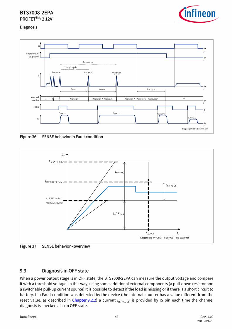
Figure 36 adds the behavior of SENSE signal to the timing diagram seen in Figure 28, while Figure 37 shows therelation between IIS = IL / kILIS, IIS(SAT) and IIS(FAULT).
t
IN
IL
0 1Internal counter
t
t
Diagnosis_PROFET_IISFAULT_load.emf
t
DEN
t
IIS
I IS(FAULT )
IL / kILIS
tIS(FAULT )_D
2
IIS(FAULT )
0
IL(OVL)
Data Sheet 43 Rev. 1.00 2016-09-20
BTS7008-2EPAPROFETTM+2 12V
Diagnosis
Figure 36 SENSE behavior in Fault condition
Figure 37 SENSE behavior - overview
9.3 Diagnosis in OFF stateWhen a power output stage is in OFF state, the BTS7008-2EPA can measure the output voltage and compareit with a threshold voltage. In this way, using some additional external components (a pull-down resistor anda switchable pull-up current source) it is possible to detect if the load is missing or if there is a short circuit tobattery. If a Fault condition was detected by the device (the internal counter has a value different from thereset value, as described in Chapter 9.2.2) a current IIS(FAULT) is provided by IS pin each time the channeldiagnosis is checked also in OFF state.
t
IN
tRETRY
Short circuit to ground
IL
0 1 nRETRY(CR)Internal counter
n RETRY(CR) + nRETRY(NT ) nRETRY(CR) + (nRETRY(CYC) * nRETRY(NT ))
tDELAY(CR)tRETRY
0
nRETRY(CR) nRETRY(NT)
"retry" cycle
nRETRY(NT)
t
t
t
Diagnosis_PROFET_IISFAULT.emf
t
DEN
t
IIS
I IS(FAULT ) IIS(FAULT )
IL / k ILIS
nRETRY(CYC)
IIS(FAULT )
Diagnosis_PROFET_IISFAULT_IISSAT.emf
IIS
IL
I IS(SAT )
IIS(FAULT )
IL / k ILIS
I IS(SAT ),min = IIS(FAULT ),min
I IS(FAULT ),max
IIS(SAT ),max
IL(OVL)
Data Sheet 44 Rev. 1.00 2016-09-20
BTS7008-2EPAPROFETTM+2 12V
Diagnosis
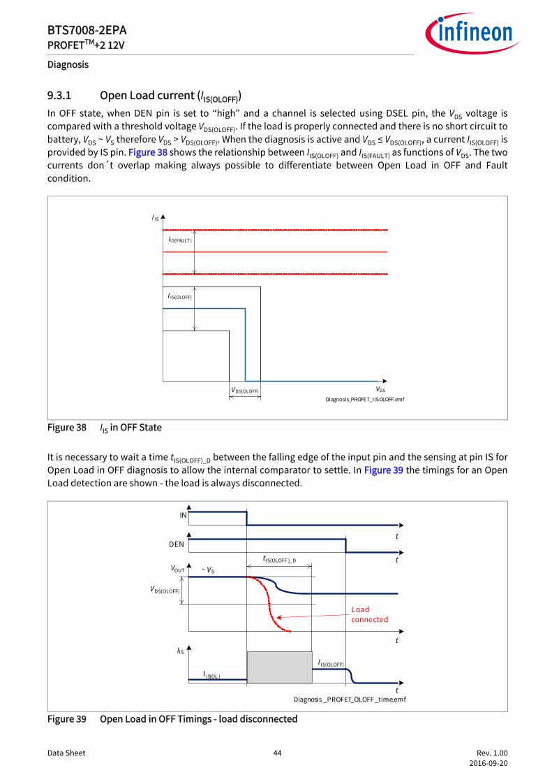
9.3.1 Open Load current (IIS(OLOFF))In OFF state, when DEN pin is set to “high” and a channel is selected using DSEL pin, the VDS voltage iscompared with a threshold voltage VDS(OLOFF). If the load is properly connected and there is no short circuit tobattery, VDS ~ VS therefore VDS > VDS(OLOFF). When the diagnosis is active and VDS ≤ VDS(OLOFF), a current IIS(OLOFF) isprovided by IS pin. Figure 38 shows the relationship between IIS(OLOFF) and IIS(FAULT) as functions of VDS. The twocurrents don´t overlap making always possible to differentiate between Open Load in OFF and Faultcondition.
Figure 38 IIS in OFF State
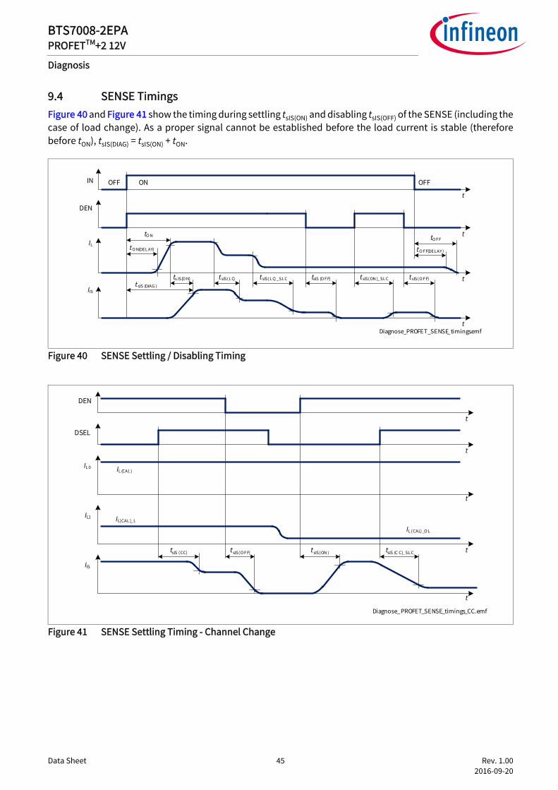
It is necessary to wait a time tIS(OLOFF)_D between the falling edge of the input pin and the sensing at pin IS forOpen Load in OFF diagnosis to allow the internal comparator to settle. In Figure 39 the timings for an OpenLoad detection are shown - the load is always disconnected.
Figure 39 Open Load in OFF Timings - load disconnected
Diagnosis_PROFET_IISOLOFF.emf
I IS
VDS
I IS(OLOFF)
VDS(OLOFF)
IIS(FAULT )
t
IN
t
DEN
VOUT ~ VS
tIS(OLOFF )_ D
t
I IS(OLOFF)
IIS
I IS(OL )
VDS(OLOFF)
t
Diagnosis _PROFET_OLOFF _time.emf
Load connected
Data Sheet 45 Rev. 1.00 2016-09-20
BTS7008-2EPAPROFETTM+2 12V
Diagnosis
9.4 SENSE TimingsFigure 40 and Figure 41 show the timing during settling tsIS(ON) and disabling tsIS(OFF) of the SENSE (including thecase of load change). As a proper signal cannot be established before the load current is stable (thereforebefore tON), tsIS(DIAG) = tsIS(ON) + tON.
Figure 40 SENSE Settling / Disabling Timing
Figure 41 SENSE Settling Timing - Channel Change
Diagnose_PROFET_SENSE_timings.emf
DEN
IIS
t
t
t
IL
t
ON
tO N
tsIS (DIAG )
tsIS(L C)
OFF
tO F F
tsIS (O F F)
IN
tO N(DEL AY) tO F F(DEL AY )
ts IS(O N) tsIS(L C)_SL C tsIS(ON )_ SL C tsIS(O F F)
OFF
Diagnose_PROFET_SENSE_timings_CC.emf
DSEL
IIS
t
t
t
IL1
t
tsIS (CC) tsIS(O F F)
DEN
tsIS(ON ) tsIS (C C)_ SL C
t
IL 0
IL(CAL )_ L
IL (CAL )
IL (CAL) _O L
Data Sheet 46 Rev. 1.00 2016-09-20
BTS7008-2EPAPROFETTM+2 12V
Diagnosis
9.5 Electrical Characteristics DiagnosisVS = 6 V to 18 V, TJ = -40 °C to +150 °CTypical values: VS = 13.5 V, TJ = 25 °CTypical resistive loads connected to the outputs for testing (unless otherwise specified):RL = 3.3 Ω
Table 20 Electrical Characteristics: Diagnosis - General
Parameter Symbol Values Unit Note or Test Condition
Number
Min. Typ. Max.
SENSE Saturation Current IIS(SAT) 4.4 – 15 mA 1)
VS - VIS ≥ 2 VSee Figure 37
1) Not subject to production test - specified by design
P_9.6.0.1
SENSE Leakage Current when Disabled
IIS(OFF) – 0.01 0.5 µA DEN = “low”IL ≥ IL(NOM)VIS = 0 V
P_9.6.0.2
SENSE Leakage Current when Enabled at TJ ≤ 85 °C
IIS(EN)_85 – 0.2 1 µA 1)
TJ ≤ 85 °CDEN = “high”IL = 0 ASee Figure 34
P_9.6.0.3
SENSE Leakage Current when Enabled at TJ = 150 °C
IIS(EN)_150 – 0.2 1 µA TJ = 150 °CDEN = “high”IL = 0 ASee Figure 34
P_9.6.0.4
SENSE Operative Range for kILIS Operation(VS - VIS)
VIS(RANGE)_k – 0.5 1 V 1)
VS = 6 VIN = DEN = “high”IL ≤ 2 * IL(NOM)
P_9.6.0.6
SENSE Operative Range for Open Load at OFF Diagnosis (VS - VIS)
VIS(RANGE)_OL – 0.5 1 V 1)
VS = 6 VIN = “low”DEN = “high”
P_9.6.0.7
SENSE Operative Range for Fault Diagnosis (VS - VIS)
VIS(RANGE)_F - 0.5 1 V 1)
VS = 6 VIN = “low”DEN = “high”counter > 0
P_9.6.0.8
Power Supply to IS Pin Clamping Voltage at TJ = -40 °C
VIS(CLAMP)_-40 33 36.5 42 V IIS = 1 mATJ = -40 °CSee Figure 17
P_9.6.0.9
Power Supply to IS Pin Clamping Voltage at TJ = 25 °C
VIS(CLAMP)_25 35 38 44 V 2)
IIS = 1 mATJ ≥ 25 °CSee Figure 17
2) Tested at TJ = 150°C
P_9.6.0.10
Data Sheet 47 Rev. 1.00 2016-09-20
BTS7008-2EPAPROFETTM+2 12V
Diagnosis
9.5.1 Electrical Characteristics Diagnosis
Table 21 Electrical Characteristics: Diagnosis
Parameter Symbol Values Unit Note or Test Condition
Number
Min. Typ. Max.
SENSE Fault Current IIS(FAULT) 4.4 5.5 10 mA See Figure 37 and Figure 38
P_9.6.1.1
SENSE Open Load in OFF Current
IIS(OLOFF) 1.9 2.5 3.5 mA See Figure 37 and Figure 38
P_9.6.1.2
SENSE Delay Time at Channel Switch ON after Last Fault Condition
tIS(FAULT)_D – 500 – µs 1)
See Figure 35P_9.6.1.3
SENSE Open Load in OFF Delay Time
tIS(OLOFF)_D 30 70 120 µs VDS < VOL(OFF)from IN falling edge to IIS = IS(OLOFF),MIN * 0.9DEN = “high”counter = 0See Figure 39
P_9.6.1.4
Open Load VDS Detection Threshold in OFF State
VDS(OLOFF) 1.3 1.8 2.3 V See Figure 38 P_9.6.1.5
SENSE Settling Time with Nominal Load Current Stable
tsIS(ON) – 5 20 µs IL = IL(CAL)from DEN rising edge to IIS = IL / (kILIS,MAX @ IL) * 0.9See Figure 40
P_9.6.1.6
SENSE Settling Time with Small Load Current Stable
tsIS(ON)_SLC – – 60 µs 1)
IL = IL(CAL)_OLfrom DEN rising edge to IIS = IL / (kILIS,MAX @ IL) * 0.9
P_9.6.1.13
SENSE Disable Time tsIS(OFF) – 5 20 µs 1)
From DEN falling edge to IIS = IIS(OFF)See Figure 40
P_9.6.1.8
SENSE Settling Time after Load Change
tsIS(LC) – 5 20 µs 1)
from IL = IL(CAL)_L to IL = IL(CAL) (see ΔkILIS(NOM))See Figure 40
P_9.6.1.9
Data Sheet 48 Rev. 1.00 2016-09-20
BTS7008-2EPAPROFETTM+2 12V
Diagnosis
9.6 Electrical Characteristics Diagnosis - Power Output Stages
9.6.1 Diagnosis Power Output Stage - 8 mΩ
SENSE Settling Time after Load Change with Small Load Current
tsIS(LC)_SLC 50 250 400 µs 1)
DEN = “high”from Load Change to IIS = IL / (kILIS,MIN @ IL) * 1.1from IL = IL(CAL) to IL = IL(CAL)_OL
P_9.6.1.14
SENSE Settling Time after Channel Change
tsIS(CC) – 5 20 µs 1)
Start channel:IL = IL(CAL)End channel:IL = IL(CAL)_L(see ΔkILIS(NOM))See Figure 41
P_9.6.1.10
SENSE Settling Time after Channel Change with Small Load Current
tsIS(CC)_SLC – – 60 µs 1)
DEN = “high”from DSEL toggling to IIS = IL / (kILIS,MIN @ IL) * 1.1Start channel:IL = IL(CAL)End Channel:IL = IL(CAL)_OL(see ΔkILIS(NOM) and ΔkILIS(OL))
P_9.6.1.15
1) Not subject to production test - specified by design
Table 22 Electrical Characteristics: Diagnosis - 8 mΩ
Parameter Symbol Values Unit Note or Test Condition
Number
Min. Typ. Max.
Open Load Output Current at IIS = 4 µA
IL(OL)_4u 8 21 35 mA IIS = IIS(OL) = 4 µASee Figure 34
P_9.7.1.1
Current Sense Ratio at IL = IL02
kILIS02 -50% 5500 +50% IL02 = 20 mA P_9.7.1.6
Current Sense Ratio at IL = IL05
kILIS05 -42% 5500 +42% IL05 = 100 mA P_9.7.1.9
Table 21 Electrical Characteristics: Diagnosis (continued)
Parameter Symbol Values Unit Note or Test Condition
Number
Min. Typ. Max.
Data Sheet 49 Rev. 1.00 2016-09-20
BTS7008-2EPAPROFETTM+2 12V
Diagnosis
Current Sense Ratio at IL = IL08
kILIS08 -40% 5500 +40% IL08 = 250 mA P_9.7.1.12
Current Sense Ratio at IL = IL11
kILIS11 -25% 5500 +25% IL11 = 1 A P_9.7.1.15
Current Sense Ratio at IL = IL14
kILIS14 -8% 5500 +8% IL14 = 2.8 A P_9.7.1.18
Current Sense Ratio at IL = IL16
kILIS16 -6% 5500 +6% IL16 = 5.5 A P_9.7.1.20
Current Sense Ratio at IL = IL18
kILIS18 -5% 5500 +5% 1)
IL18 = 10 AP_9.7.1.22
SENSE Current Derating with Low Current Calibration
ΔkILIS(OL) -30 0 +30 % 1)
IL(CAL)_OL = IL05IL(CAL)_OL_H = IL08IL(CAL)_OL_L = IL02TA(CAL) = 25 °C
P_9.7.1.27
SENSE Current Derating with Nominal Current Calibration
ΔkILIS(NOM) -4 0 +4 % 1)
IL(CAL) = IL16IL(CAL)_H = IL18IL(CAL)_L = IL14TA(CAL) = 25 °C
P_9.7.1.29
1) Not subject to production test - specified by design
Table 22 Electrical Characteristics: Diagnosis - 8 mΩ (continued)
Parameter Symbol Values Unit Note or Test Condition
Number
Min. Typ. Max.
Data Sheet 50 Rev. 1.00 2016-09-20
BTS7008-2EPAPROFETTM+2 12V
Application Information
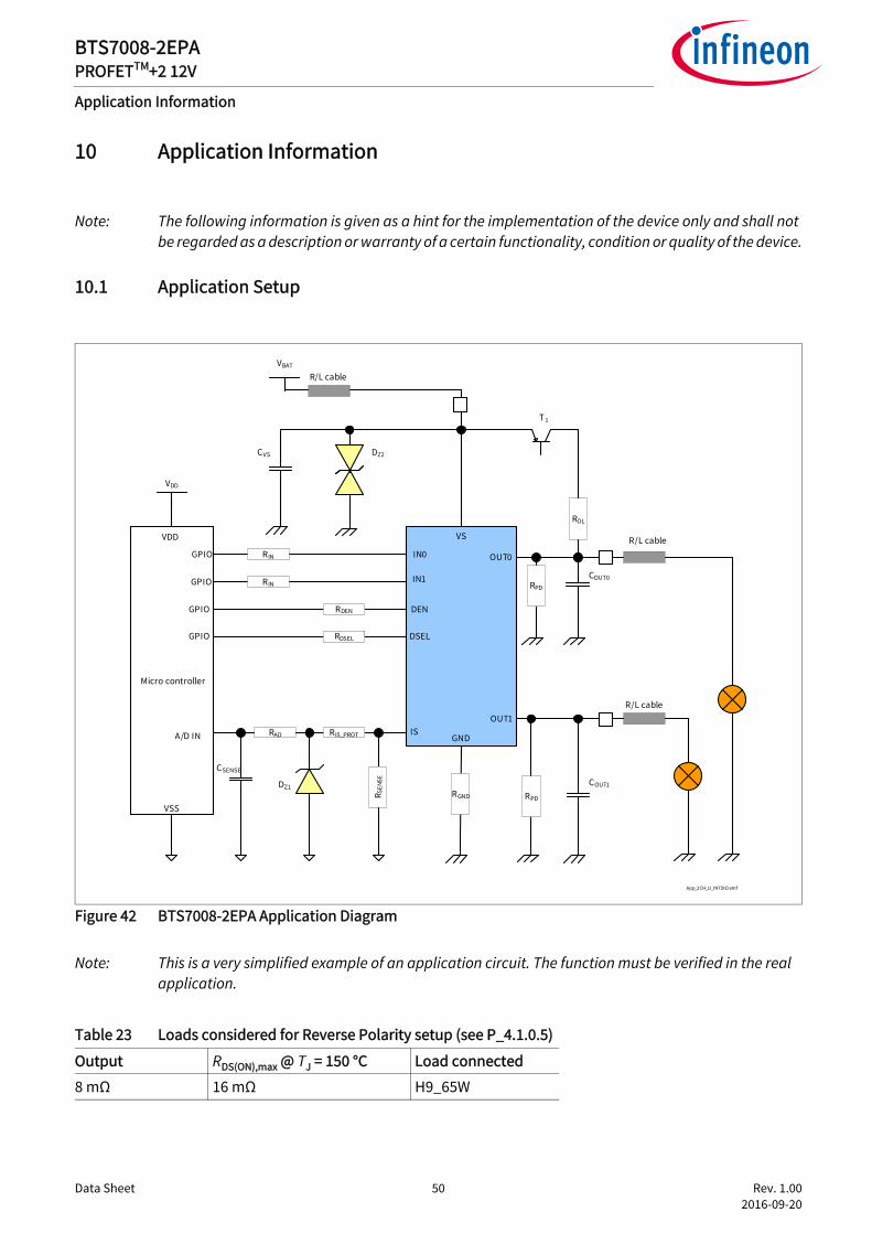
10 Application Information
Note: The following information is given as a hint for the implementation of the device only and shall not be regarded as a description or warranty of a certain functionality, condition or quality of the device.
10.1 Application Setup
Figure 42 BTS7008-2EPA Application Diagram
Note: This is a very simplified example of an application circuit. The function must be verified in the real application.
Table 23 Loads considered for Reverse Polarity setup (see P_4.1.0.5)
Output RDS(ON),max @ TJ = 150 °C Load connected
8 mΩ 16 mΩ H9_65W
GPIO
GPIO
GPIO
GPIO
A/D IN
VSS
VDD
Micro controller
IN0
IN1
DEN
DSEL
ISGND
OUT0
OUT1
VS
VBAT
CSENSE
DZ1
R/L cable
R/L cable
R/L cable
COUT1
COUT0
RIN
RIN
RDEN
RDSEL
RAD RIS_PROT
R SEN
SE
RGND
VDD
RPD
RPD
CVS
ROL
T 1
DZ2
App_2CH_LI_INTDIO.emf
Data Sheet 51 Rev. 1.00 2016-09-20
BTS7008-2EPAPROFETTM+2 12V
Application Information
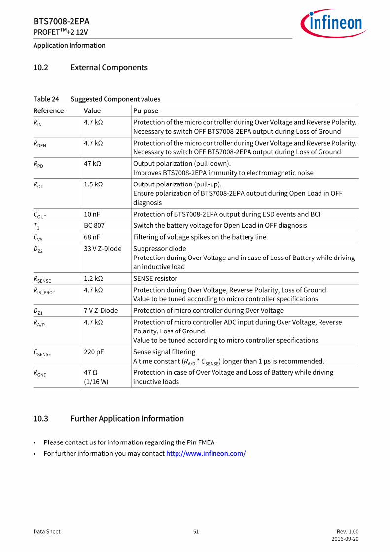
10.2 External Components
10.3 Further Application Information
• Please contact us for information regarding the Pin FMEA• For further information you may contact http://www.infineon.com/
Table 24 Suggested Component values
Reference Value Purpose
RIN 4.7 kΩ Protection of the micro controller during Over Voltage and Reverse Polarity.Necessary to switch OFF BTS7008-2EPA output during Loss of Ground
RDEN 4.7 kΩ Protection of the micro controller during Over Voltage and Reverse Polarity.Necessary to switch OFF BTS7008-2EPA output during Loss of Ground
RPD 47 kΩ Output polarization (pull-down).Improves BTS7008-2EPA immunity to electromagnetic noise
ROL 1.5 kΩ Output polarization (pull-up).Ensure polarization of BTS7008-2EPA output during Open Load in OFF diagnosis
COUT 10 nF Protection of BTS7008-2EPA output during ESD events and BCI
T1 BC 807 Switch the battery voltage for Open Load in OFF diagnosis
CVS 68 nF Filtering of voltage spikes on the battery line
DZ2 33 V Z-Diode Suppressor diodeProtection during Over Voltage and in case of Loss of Battery while driving an inductive load
RSENSE 1.2 kΩ SENSE resistor
RIS_PROT 4.7 kΩ Protection during Over Voltage, Reverse Polarity, Loss of Ground.Value to be tuned according to micro controller specifications.
DZ1 7 V Z-Diode Protection of micro controller during Over Voltage
RA/D 4.7 kΩ Protection of micro controller ADC input during Over Voltage, Reverse Polarity, Loss of Ground.Value to be tuned according to micro controller specifications.
CSENSE 220 pF Sense signal filteringA time constant (RA/D * CSENSE) longer than 1 µs is recommended.
RGND 47 Ω(1/16 W)
Protection in case of Over Voltage and Loss of Battery while driving inductive loads
Data Sheet 52 Rev. 1.00 2016-09-20
BTS7008-2EPAPROFETTM+2 12V
Package Outlines
11 Package Outlines
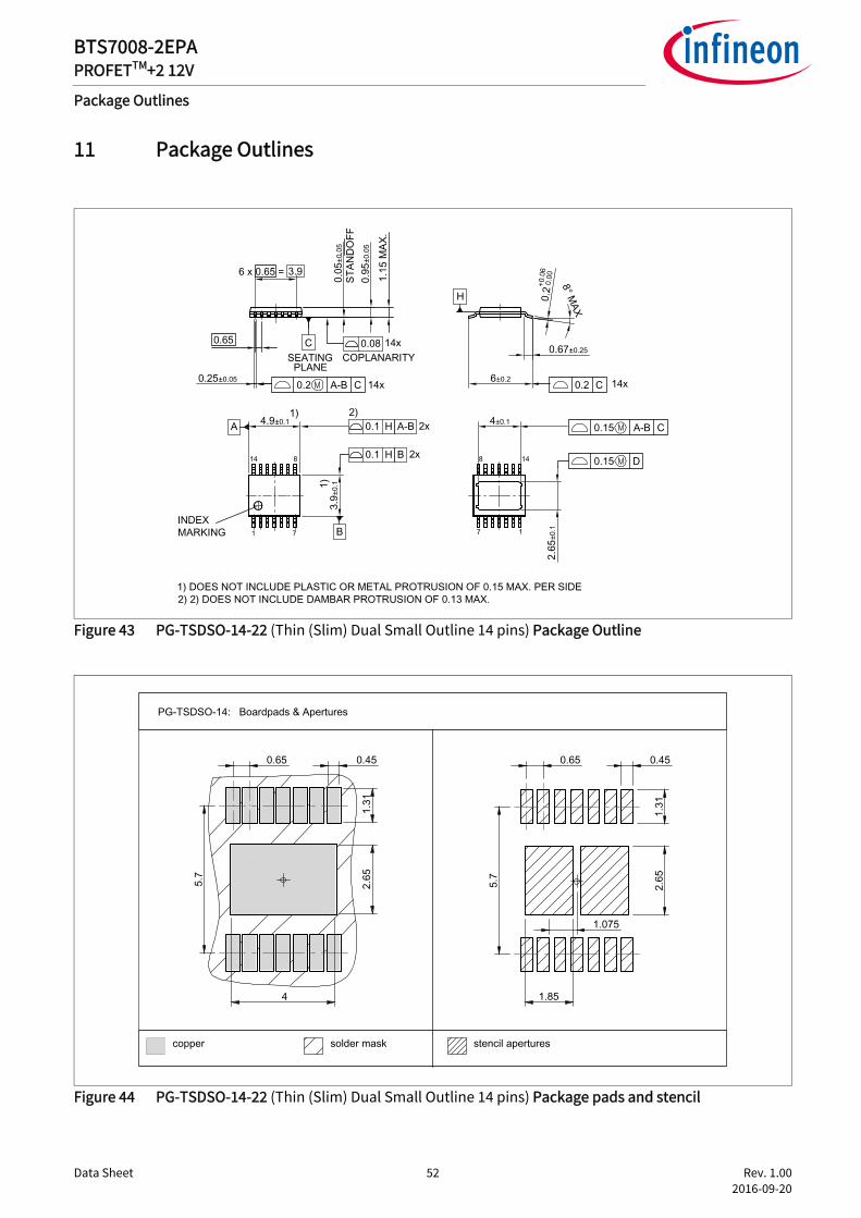
Figure 43 PG-TSDSO-14-22 (Thin (Slim) Dual Small Outline 14 pins) Package Outline
Figure 44 PG-TSDSO-14-22 (Thin (Slim) Dual Small Outline 14 pins) Package pads and stencil

Data Sheet 53 Rev. 1.00 2016-09-20
BTS7008-2EPAPROFETTM+2 12V
Package Outlines
Green Product (RoHS compliant)
To meet the world-wide customer requirements for environmentally friendly products and to be compliantwith government regulations the device is available as a green product. Green products are RoHS-Compliant(i.e Pb-free finish on leads and suitable for Pb-free soldering according to IPC/JEDEC J-STD-020).
For further information on alternative packages, please visit our website:http://www.infineon.com/packages. Dimensions in mm

Data Sheet 54 Rev. 1.00 2016-09-20
BTS7008-2EPAPROFETTM+2 12V
Revision History
12 Revision History
Table 25 BTS7008-2EPA - List of changes
Revision Changes
Rev. 1.00,2016-09-20
Data Sheet available
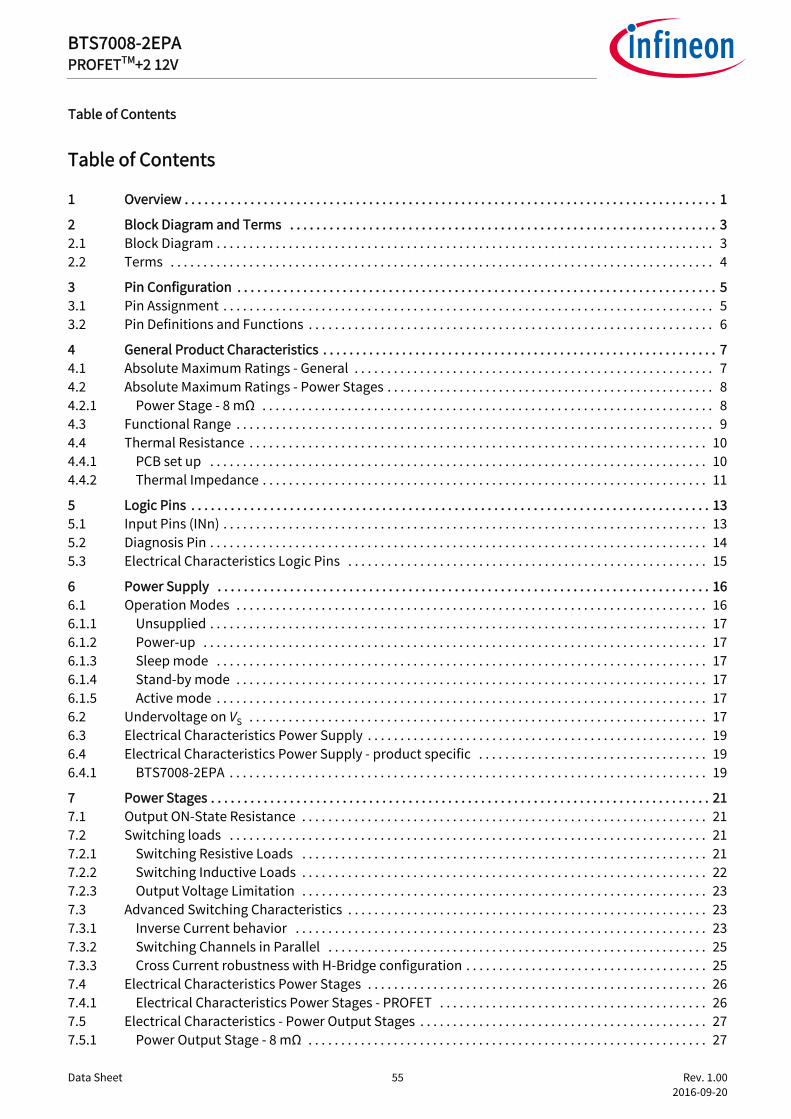
Table of Contents
Data Sheet 55 Rev. 1.00 2016-09-20
BTS7008-2EPAPROFETTM+2 12V
1 Overview . . . . . . . . . . . . . . . . . . . . . . . . . . . . . . . . . . . . . . . . . . . . . . . . . . . . . . . . . . . . . . . . . . . . . . . . . . . . . . . . . 1
2 Block Diagram and Terms . . . . . . . . . . . . . . . . . . . . . . . . . . . . . . . . . . . . . . . . . . . . . . . . . . . . . . . . . . . . . . . . . 32.1 Block Diagram . . . . . . . . . . . . . . . . . . . . . . . . . . . . . . . . . . . . . . . . . . . . . . . . . . . . . . . . . . . . . . . . . . . . . . . . . . . . 32.2 Terms . . . . . . . . . . . . . . . . . . . . . . . . . . . . . . . . . . . . . . . . . . . . . . . . . . . . . . . . . . . . . . . . . . . . . . . . . . . . . . . . . . . 4
3 Pin Configuration . . . . . . . . . . . . . . . . . . . . . . . . . . . . . . . . . . . . . . . . . . . . . . . . . . . . . . . . . . . . . . . . . . . . . . . . . 53.1 Pin Assignment . . . . . . . . . . . . . . . . . . . . . . . . . . . . . . . . . . . . . . . . . . . . . . . . . . . . . . . . . . . . . . . . . . . . . . . . . . . 53.2 Pin Definitions and Functions . . . . . . . . . . . . . . . . . . . . . . . . . . . . . . . . . . . . . . . . . . . . . . . . . . . . . . . . . . . . . . 6
4 General Product Characteristics . . . . . . . . . . . . . . . . . . . . . . . . . . . . . . . . . . . . . . . . . . . . . . . . . . . . . . . . . . . . 74.1 Absolute Maximum Ratings - General . . . . . . . . . . . . . . . . . . . . . . . . . . . . . . . . . . . . . . . . . . . . . . . . . . . . . . . 74.2 Absolute Maximum Ratings - Power Stages . . . . . . . . . . . . . . . . . . . . . . . . . . . . . . . . . . . . . . . . . . . . . . . . . . 84.2.1 Power Stage - 8 mΩ . . . . . . . . . . . . . . . . . . . . . . . . . . . . . . . . . . . . . . . . . . . . . . . . . . . . . . . . . . . . . . . . . . . . . 84.3 Functional Range . . . . . . . . . . . . . . . . . . . . . . . . . . . . . . . . . . . . . . . . . . . . . . . . . . . . . . . . . . . . . . . . . . . . . . . . . 94.4 Thermal Resistance . . . . . . . . . . . . . . . . . . . . . . . . . . . . . . . . . . . . . . . . . . . . . . . . . . . . . . . . . . . . . . . . . . . . . . 104.4.1 PCB set up . . . . . . . . . . . . . . . . . . . . . . . . . . . . . . . . . . . . . . . . . . . . . . . . . . . . . . . . . . . . . . . . . . . . . . . . . . . . 104.4.2 Thermal Impedance . . . . . . . . . . . . . . . . . . . . . . . . . . . . . . . . . . . . . . . . . . . . . . . . . . . . . . . . . . . . . . . . . . . . 11
5 Logic Pins . . . . . . . . . . . . . . . . . . . . . . . . . . . . . . . . . . . . . . . . . . . . . . . . . . . . . . . . . . . . . . . . . . . . . . . . . . . . . . . 135.1 Input Pins (INn) . . . . . . . . . . . . . . . . . . . . . . . . . . . . . . . . . . . . . . . . . . . . . . . . . . . . . . . . . . . . . . . . . . . . . . . . . . 135.2 Diagnosis Pin . . . . . . . . . . . . . . . . . . . . . . . . . . . . . . . . . . . . . . . . . . . . . . . . . . . . . . . . . . . . . . . . . . . . . . . . . . . . 145.3 Electrical Characteristics Logic Pins . . . . . . . . . . . . . . . . . . . . . . . . . . . . . . . . . . . . . . . . . . . . . . . . . . . . . . . 15
6 Power Supply . . . . . . . . . . . . . . . . . . . . . . . . . . . . . . . . . . . . . . . . . . . . . . . . . . . . . . . . . . . . . . . . . . . . . . . . . . . 166.1 Operation Modes . . . . . . . . . . . . . . . . . . . . . . . . . . . . . . . . . . . . . . . . . . . . . . . . . . . . . . . . . . . . . . . . . . . . . . . . 166.1.1 Unsupplied . . . . . . . . . . . . . . . . . . . . . . . . . . . . . . . . . . . . . . . . . . . . . . . . . . . . . . . . . . . . . . . . . . . . . . . . . . . . 176.1.2 Power-up . . . . . . . . . . . . . . . . . . . . . . . . . . . . . . . . . . . . . . . . . . . . . . . . . . . . . . . . . . . . . . . . . . . . . . . . . . . . . 176.1.3 Sleep mode . . . . . . . . . . . . . . . . . . . . . . . . . . . . . . . . . . . . . . . . . . . . . . . . . . . . . . . . . . . . . . . . . . . . . . . . . . . 176.1.4 Stand-by mode . . . . . . . . . . . . . . . . . . . . . . . . . . . . . . . . . . . . . . . . . . . . . . . . . . . . . . . . . . . . . . . . . . . . . . . . 176.1.5 Active mode . . . . . . . . . . . . . . . . . . . . . . . . . . . . . . . . . . . . . . . . . . . . . . . . . . . . . . . . . . . . . . . . . . . . . . . . . . . 176.2 Undervoltage on VS . . . . . . . . . . . . . . . . . . . . . . . . . . . . . . . . . . . . . . . . . . . . . . . . . . . . . . . . . . . . . . . . . . . . . . 176.3 Electrical Characteristics Power Supply . . . . . . . . . . . . . . . . . . . . . . . . . . . . . . . . . . . . . . . . . . . . . . . . . . . . 196.4 Electrical Characteristics Power Supply - product specific . . . . . . . . . . . . . . . . . . . . . . . . . . . . . . . . . . . 196.4.1 BTS7008-2EPA . . . . . . . . . . . . . . . . . . . . . . . . . . . . . . . . . . . . . . . . . . . . . . . . . . . . . . . . . . . . . . . . . . . . . . . . . 19
7 Power Stages . . . . . . . . . . . . . . . . . . . . . . . . . . . . . . . . . . . . . . . . . . . . . . . . . . . . . . . . . . . . . . . . . . . . . . . . . . . . 217.1 Output ON-State Resistance . . . . . . . . . . . . . . . . . . . . . . . . . . . . . . . . . . . . . . . . . . . . . . . . . . . . . . . . . . . . . . 217.2 Switching loads . . . . . . . . . . . . . . . . . . . . . . . . . . . . . . . . . . . . . . . . . . . . . . . . . . . . . . . . . . . . . . . . . . . . . . . . . 217.2.1 Switching Resistive Loads . . . . . . . . . . . . . . . . . . . . . . . . . . . . . . . . . . . . . . . . . . . . . . . . . . . . . . . . . . . . . . 217.2.2 Switching Inductive Loads . . . . . . . . . . . . . . . . . . . . . . . . . . . . . . . . . . . . . . . . . . . . . . . . . . . . . . . . . . . . . . 227.2.3 Output Voltage Limitation . . . . . . . . . . . . . . . . . . . . . . . . . . . . . . . . . . . . . . . . . . . . . . . . . . . . . . . . . . . . . . 237.3 Advanced Switching Characteristics . . . . . . . . . . . . . . . . . . . . . . . . . . . . . . . . . . . . . . . . . . . . . . . . . . . . . . . 237.3.1 Inverse Current behavior . . . . . . . . . . . . . . . . . . . . . . . . . . . . . . . . . . . . . . . . . . . . . . . . . . . . . . . . . . . . . . . 237.3.2 Switching Channels in Parallel . . . . . . . . . . . . . . . . . . . . . . . . . . . . . . . . . . . . . . . . . . . . . . . . . . . . . . . . . . 257.3.3 Cross Current robustness with H-Bridge configuration . . . . . . . . . . . . . . . . . . . . . . . . . . . . . . . . . . . . . 257.4 Electrical Characteristics Power Stages . . . . . . . . . . . . . . . . . . . . . . . . . . . . . . . . . . . . . . . . . . . . . . . . . . . . 267.4.1 Electrical Characteristics Power Stages - PROFET . . . . . . . . . . . . . . . . . . . . . . . . . . . . . . . . . . . . . . . . . 267.5 Electrical Characteristics - Power Output Stages . . . . . . . . . . . . . . . . . . . . . . . . . . . . . . . . . . . . . . . . . . . . 277.5.1 Power Output Stage - 8 mΩ . . . . . . . . . . . . . . . . . . . . . . . . . . . . . . . . . . . . . . . . . . . . . . . . . . . . . . . . . . . . . 27
Table of Contents
Table of Contents
Data Sheet 56 Rev. 1.00 2016-09-20
BTS7008-2EPAPROFETTM+2 12V
8 Protection . . . . . . . . . . . . . . . . . . . . . . . . . . . . . . . . . . . . . . . . . . . . . . . . . . . . . . . . . . . . . . . . . . . . . . . . . . . . . . 298.1 Over Temperature Protection . . . . . . . . . . . . . . . . . . . . . . . . . . . . . . . . . . . . . . . . . . . . . . . . . . . . . . . . . . . . . 298.2 Overload Protection . . . . . . . . . . . . . . . . . . . . . . . . . . . . . . . . . . . . . . . . . . . . . . . . . . . . . . . . . . . . . . . . . . . . . 308.3 Protection and Diagnosis in case of Fault . . . . . . . . . . . . . . . . . . . . . . . . . . . . . . . . . . . . . . . . . . . . . . . . . . 328.3.1 Retry Strategy . . . . . . . . . . . . . . . . . . . . . . . . . . . . . . . . . . . . . . . . . . . . . . . . . . . . . . . . . . . . . . . . . . . . . . . . . 328.4 Additional protections . . . . . . . . . . . . . . . . . . . . . . . . . . . . . . . . . . . . . . . . . . . . . . . . . . . . . . . . . . . . . . . . . . . 358.4.1 Reverse Polarity Protection . . . . . . . . . . . . . . . . . . . . . . . . . . . . . . . . . . . . . . . . . . . . . . . . . . . . . . . . . . . . . 358.4.2 Over Voltage Protection . . . . . . . . . . . . . . . . . . . . . . . . . . . . . . . . . . . . . . . . . . . . . . . . . . . . . . . . . . . . . . . . 368.5 Protection against loss of connection . . . . . . . . . . . . . . . . . . . . . . . . . . . . . . . . . . . . . . . . . . . . . . . . . . . . . . 368.5.1 Loss of Battery and Loss of Load . . . . . . . . . . . . . . . . . . . . . . . . . . . . . . . . . . . . . . . . . . . . . . . . . . . . . . . . . 368.5.2 Loss of Ground . . . . . . . . . . . . . . . . . . . . . . . . . . . . . . . . . . . . . . . . . . . . . . . . . . . . . . . . . . . . . . . . . . . . . . . . 368.6 Electrical Characteristics Protection . . . . . . . . . . . . . . . . . . . . . . . . . . . . . . . . . . . . . . . . . . . . . . . . . . . . . . . 378.6.1 Electrical Characteristics Protection . . . . . . . . . . . . . . . . . . . . . . . . . . . . . . . . . . . . . . . . . . . . . . . . . . . . . 378.7 Electrical Characteristics Protection - Power Output Stages . . . . . . . . . . . . . . . . . . . . . . . . . . . . . . . . . . 388.7.1 Protection Power Output Stage - 8 mΩ . . . . . . . . . . . . . . . . . . . . . . . . . . . . . . . . . . . . . . . . . . . . . . . . . . . 38
9 Diagnosis . . . . . . . . . . . . . . . . . . . . . . . . . . . . . . . . . . . . . . . . . . . . . . . . . . . . . . . . . . . . . . . . . . . . . . . . . . . . . . . 399.1 Overview . . . . . . . . . . . . . . . . . . . . . . . . . . . . . . . . . . . . . . . . . . . . . . . . . . . . . . . . . . . . . . . . . . . . . . . . . . . . . . . 399.1.1 SENSE signal truth table . . . . . . . . . . . . . . . . . . . . . . . . . . . . . . . . . . . . . . . . . . . . . . . . . . . . . . . . . . . . . . . . 409.2 Diagnosis in ON state . . . . . . . . . . . . . . . . . . . . . . . . . . . . . . . . . . . . . . . . . . . . . . . . . . . . . . . . . . . . . . . . . . . . 409.2.1 Current Sense (kILIS) . . . . . . . . . . . . . . . . . . . . . . . . . . . . . . . . . . . . . . . . . . . . . . . . . . . . . . . . . . . . . . . . . . . . 419.2.2 Fault Current (IIS(FAULT)) . . . . . . . . . . . . . . . . . . . . . . . . . . . . . . . . . . . . . . . . . . . . . . . . . . . . . . . . . . . . . . . . . 429.3 Diagnosis in OFF state . . . . . . . . . . . . . . . . . . . . . . . . . . . . . . . . . . . . . . . . . . . . . . . . . . . . . . . . . . . . . . . . . . . . 439.3.1 Open Load current (IIS(OLOFF)) . . . . . . . . . . . . . . . . . . . . . . . . . . . . . . . . . . . . . . . . . . . . . . . . . . . . . . . . . . . . 449.4 SENSE Timings . . . . . . . . . . . . . . . . . . . . . . . . . . . . . . . . . . . . . . . . . . . . . . . . . . . . . . . . . . . . . . . . . . . . . . . . . . 459.5 Electrical Characteristics Diagnosis . . . . . . . . . . . . . . . . . . . . . . . . . . . . . . . . . . . . . . . . . . . . . . . . . . . . . . . . 469.5.1 Electrical Characteristics Diagnosis . . . . . . . . . . . . . . . . . . . . . . . . . . . . . . . . . . . . . . . . . . . . . . . . . . . . . . 479.6 Electrical Characteristics Diagnosis - Power Output Stages . . . . . . . . . . . . . . . . . . . . . . . . . . . . . . . . . . 489.6.1 Diagnosis Power Output Stage - 8 mΩ . . . . . . . . . . . . . . . . . . . . . . . . . . . . . . . . . . . . . . . . . . . . . . . . . . . . 48
10 Application Information . . . . . . . . . . . . . . . . . . . . . . . . . . . . . . . . . . . . . . . . . . . . . . . . . . . . . . . . . . . . . . . . . . 5010.1 Application Setup . . . . . . . . . . . . . . . . . . . . . . . . . . . . . . . . . . . . . . . . . . . . . . . . . . . . . . . . . . . . . . . . . . . . . . . 5010.2 External Components . . . . . . . . . . . . . . . . . . . . . . . . . . . . . . . . . . . . . . . . . . . . . . . . . . . . . . . . . . . . . . . . . . . . 5110.3 Further Application Information . . . . . . . . . . . . . . . . . . . . . . . . . . . . . . . . . . . . . . . . . . . . . . . . . . . . . . . . . . 51
11 Package Outlines . . . . . . . . . . . . . . . . . . . . . . . . . . . . . . . . . . . . . . . . . . . . . . . . . . . . . . . . . . . . . . . . . . . . . . . . 52
12 Revision History . . . . . . . . . . . . . . . . . . . . . . . . . . . . . . . . . . . . . . . . . . . . . . . . . . . . . . . . . . . . . . . . . . . . . . . . . 54
Table of Contents . . . . . . . . . . . . . . . . . . . . . . . . . . . . . . . . . . . . . . . . . . . . . . . . . . . . . . . . . . . . . . . . . . . . . . . . 55
Trademarks of Infineon Technologies AGµHVIC™, µIPM™, µPFC™, AU-ConvertIR™, AURIX™, C166™, CanPAK™, CIPOS™, CIPURSE™, CoolDP™, CoolGaN™, COOLiR™, CoolMOS™, CoolSET™, CoolSiC™,DAVE™, DI-POL™, DirectFET™, DrBlade™, EasyPIM™, EconoBRIDGE™, EconoDUAL™, EconoPACK™, EconoPIM™, EiceDRIVER™, eupec™, FCOS™, GaNpowIR™,HEXFET™, HITFET™, HybridPACK™, iMOTION™, IRAM™, ISOFACE™, IsoPACK™, LEDrivIR™, LITIX™, MIPAQ™, ModSTACK™, my-d™, NovalithIC™, OPTIGA™,OptiMOS™, ORIGA™, PowIRaudio™, PowIRStage™, PrimePACK™, PrimeSTACK™, PROFET™, PRO-SIL™, RASIC™, REAL3™, SmartLEWIS™, SOLID FLASH™,SPOC™, StrongIRFET™, SupIRBuck™, TEMPFET™, TRENCHSTOP™, TriCore™, UHVIC™, XHP™, XMC™.
Trademarks updated November 2015
Other TrademarksAll referenced product or service names and trademarks are the property of their respective owners.
Edition 2016-09-20Published by Infineon Technologies AG81726 Munich, Germany
© 2016 Infineon Technologies AG.All Rights Reserved.
Do you have a question about any aspect of this document?Email: [email protected]
Document reference
IMPORTANT NOTICEThe information given in this document shall in noevent be regarded as a guarantee of conditions orcharacteristics ("Beschaffenheitsgarantie"). With respect to any examples, hints or any typicalvalues stated herein and/or any information regardingthe application of the product, Infineon Technologieshereby disclaims any and all warranties and liabilitiesof any kind, including without limitation warranties ofnon-infringement of intellectual property rights of anythird party. In addition, any information given in this document issubject to customer's compliance with its obligationsstated in this document and any applicable legalrequirements, norms and standards concerningcustomer's products and any use of the product ofInfineon Technologies in customer's applications. The data contained in this document is exclusivelyintended for technically trained staff. It is theresponsibility of customer's technical departments toevaluate the suitability of the product for the intendedapplication and the completeness of the productinformation given in this document with respect tosuch application.
For further information on technology, delivery termsand conditions and prices, please contact the nearestInfineon Technologies Office (www.infineon.com).
WARNINGS
Due to technical requirements products may containdangerous substances. For information on the typesin question please contact your nearest InfineonTechnologies office.
Except as otherwise explicitly approved by InfineonTechnologies in a written document signed byauthorized representatives of Infineon Technologies,Infineon Technologies’ products may not be used inany applications where a failure of the product or anyconsequences of the use thereof can reasonably beexpected to result in personal injury.
Please read the Important Notice and Warnings at the end of this document

Mouser Electronics
Authorized Distributor
Click to View Pricing, Inventory, Delivery & Lifecycle Information: Infineon:
BTS70082EPAXUMA1