Embed Size (px)
Citation preview

4. CONCLUSIONS
In summary, CMOS compatible ICP deep trench technology is
used to remove the silicon underneath a monopole antenna imple-
mented in 0.18-lm CMOS process. The experimental results show
that the input return losses can be improved by as large as 5 dB and
power transfer ratio can be increased from 0.87 to 0.96 because of
the reduction of dielectric losses by ICP etching. Therefore, high-
performance fully integrated silicon MMICs including antennas
can be expected with the help of this ICP technology.
ACKNOWLEDGMENTS
The authors thank the National Chip Implementation Center and
UMC for IC implementation and the National Nano-Device Labo-
ratory for measurement supports. Financial supports from national
science council under contract no. NSC 97-2221-E-002 -153 -MY3
and no. NSC 99-2218-E-182-010 are also appreciated.
REFERENCES
1. C.H. Doan, S. Emami, A.M. Nikenejad, and R.W. Broadersoen,
Millimeter-wave CMOS Design, IEEE J Solid-State Circuits 40
(2005), 144–155.
2. K.K.O, K. Kim, B.A. Floyd, J.L. Mehta, H. Yoon, C.-M. Hung, D.
Bravo, T.O. Dickson, X. Guo, R. Li, N. Trichy, J. Caserta, W.R. Bom-
stad, II, J. Branch, D.-J. Yang, J. Bohorques, E. Seok, L. Gao, A. Suga-
vanam, J.-J. Lin, and J. E. Brewer, On-chip antenna in silicon ICs and
their application, IEEE T Electron Devices 52 (2005), 1312–1323.
3. B. Rong, J.N. Burghartz, L.K. Nanver, B. Rejaei, and M. van der
Zwan, Surface-passivated high-resistivity silicon substrates for
RFICs, IEEE Electron Device Lett 25 (2004), 176–178.
4. I.-Y Chen, C.-U. Huang, H.J.H. Chen, C.F. Jou, and R.-S. Huang,
A 2.4 GHz and 5.2 GHz dual-band antenna fabricated on flexible
parylene membrane, Jpn J Appl Phys 44 (1997), 8356–8361.
5. I.K. Itotia and R.F. Drayton, Porosity effects on coplanar waveguide
porous silicon interconnects, IEEE MTT-S Digest 2002, pp. 681–684.
6. M.T. Yang, T.J. Yeh, H.M. Hsu, P.C. Ho, Y.J. Wang, Y.T. Chia,
and D.D.L. Tang, Characterization and model of high quality factor
and broadband integrated inductor on Si-substrate, IEEE MTT-S
Digest 2003, 1283–1286.
7. T. Wang, Y.-S. Lin, and S.-S. Lu, An ultralow-loss and broadband
micromachined RF inductor for RFIC input-matching applications,
IEEE T Electron Devices 53 (2006), 568–570.
8. T. Wang, C.-H. Chen, Y.-S. Lin, and S.-S. Lu, A micromachined
CMOS distributed amplifier by CMOS compatible ICP deep-trench
technology, IEEE Electron Device Lett 27 (2006), 291–293.
9. T. Wang, H.-C. Chen, H.-W. Chiu, Y.-S. Lin, G. W. Huang, and
S.-S. Lu, Micromachined CMOS LNA and VCO by CMOS-com-
patible ICP deep trench technology, IEEE T Microwave Theory
Tech 54 (2006), 580–588.
10. W.L. Stutzman and G.A. Thiele, Antenna theory and design, 2nd
ed., Wiley, New York, NY, 1998, p. 220.
VC 2011 Wiley Periodicals, Inc.
A 3.4/5.5 GHZ DUAL-BAND NOTCHEDUWB PRINTED MONOPOLE ANTENNAWITH TWO OPEN-CIRCUITED STUBSIN THE MICROSTRIP FEEDLINE
Jyoti Ranjan Panda and Rakhesh Singh KshetrimayumDepartment of Electronics and Electrical Engineering, IndianInstitute of Technology Guwahati, 781039, India; Correspondingauthor: [email protected]
Received 8 March 2011
ABSTRACT: An ultrawideband (UWB) printed monopole antenna
(PMA) for the 3.4/5.5 GHz dual-band notched operation is presented.
The antenna has a rectangular radiating element with a symmetricalstaircase structure in the bottom or feed region and fed by a 50-Xmicrostrip line. By introducing two open-circuited stubs from the twosides of the microstrip feedline, dual band-notched characteristics in theWiMAX/WLAN bands are achieved. The proposed antenna is effectively
designed, simulated, fabricated, and measured providing broadbandimpedance matching, appropriate gain, and stable radiation patterncharacteristics. An UWB and single band-notched UWB antenna are
also fabricated for comparison. The proposed UWB antenna isinvestigated in time domain, and it has been observed experimentally
that the received fifth derivative of Gaussian pulse is not distorted inthe main waveform but some amount of ringing is observed. VC 2011
Wiley Periodicals, Inc. Microwave Opt Technol Lett 53:2973–2978,
2011; View this article online at wileyonlinelibrary.com.
DOI 10.1002/mop.26380
Key words: band-notched characteristics; microstrip line; open-
circuited stubs; UWB antenna
1. INTRODUCTION
Federal Communication Commission’s (FCC)’s ruling in Febru-
ary 2002 [1] for the commercial use of huge band from 3.1 to
10.6 GHz has completely revolutionized the wireless and high
speed data communication world. This huge bandwidth from 3.1
to 10.6 GHz is assigned as the ultrawideband (UWB) spectrum
by FCC. But along with the vast operating bandwidth of the
UWB antenna (3.1–10.6 GHz), there exist some narrowband
(NB) wireless services, which occupy some of the frequency
bands in the UWB bands. The most well known among them is
wireless local area network (WLAN) IEEE802.11a and HIPER-
LAN/2 WLAN operating in 5–6 GHz band. Apart from WLAN,
in some European and Asian countries, world interoperability
for microwave access (WiMAX) service from 3.3 to 3.6 GHz
also shares spectrum with the UWB. In some antenna designs,
the UWB antenna uses filters to notch out the interfering bands.
However, the use of filters increases the complexity of
the UWB system and also increases the weight and size of the
UWB transreceivers. Hence, it has been necessitated to design
UWB antenna with dual band-notched characteristics both in
3.3–3.6 GHz and 5–6 GHz to mitigate the interference between
the narrowband wireless systems and UWB systems. Till now,
many designs of the UWB band-notched antennas are proposed
to alleviate the disturbance caused by the WLAN with the UWB
system.
Based on the background of the structures of various UWB
notch-antennas [2–7], this letter proposes a simple and compact
microstrip line fed UWB PMA (2.63–13.1 GHz) with dual
band-notched characteristics in 3.48 GHz (3.03–4.04 GHz) and
5.59 GHz (4.76–6.29 GHz). The dual band-notched characteris-
tic in the proposed antenna has been achieved by introducing
two open-circuited stubs from the two sides of the microstrip
feedline. By adjusting the length of the two open circuited stubs
approximately to one quarter of the guided wavelength (kg) of
the required notch frequency, a destructive interference of the
current distribution takes place causing the antenna nonradiating
at that notch frequency. The tuning of the central notch fre-
quency can be done suitably by adjusting the total length of the
two open-circuited stubs. The optimization of the design and the
subsequent simulation is done using IE3D software [8]. The pro-
posed antenna provides measured impedance bandwidth of 3.1–
10.6 GHz with VSWR � 2, except the bandwidths of 3.03–4.04
GHz for WiMAX systems and 4.76–6.29 GHz for IEEE802.11a
and HIPERLAN/2 WLAN systems. The appropriate gain and
stable radiation patterns are also observed experimentally.
DOI 10.1002/mop MICROWAVE AND OPTICAL TECHNOLOGY LETTERS / Vol. 53, No. 12, December 2011 2973

In this letter, a compact UWB PMA of area 30 � 35 mm2 is
proposed. Open-circuited stubs on two sides of the microstrip
feedline create dual band-notched characteristics for coexistence
without interference between the NB and the UWB wireless sys-
tems. Detailed time and frequency domain simulation as well as
experimental results along with a brief discussion on the antenna
designs are presented to demonstrate the performance of the pro-
posed antenna.
2. UWB DUAL BAND-NOTCHED ANTENNA DESIGN ANDRESULTS
Figure 1 shows the geometry and configuration of a UWB dual-
band notched antenna. The antenna (referred to as antenna 3 in
this letter) was fabricated on an h ¼ 1.6 mm FR4 epoxy sub-
strate with the dielectric constant er ¼ 4.4 and loss tangent tan d¼ 0.002. As shown in the figure, the shape of the radiating ele-
ment is rectangular, and there is a stair case structure symmetri-
cally the two bottom corners of the radiating element. The
design parameters are given in the Figure 1. The staircase struc-
ture improves the impedance matching and the bandwidth of the
antenna 3. The fabricated prototype of antenna 3 is shown inside
the Figure 2. By introducing two open-circuited stubs on the
both side of the microstrip feedline, the appropriate dual band-
notched function both in 3.3–3.6 GHz and 5–6 GHz are
achieved. The open circuited stub on the left side of the micro-
strip feedline provides the notch band at 3.4 GHz and the open
circuited stub on the right side of the microstrip feedline pro-
vides another one at 5.5 GHz, each of the total length of the
open-circuited stubs are approximately one quarter the guided
wavelength (kg) of the required notch frequency.
The guided wavelength (kg) at 5.5 GHz was found to be
33.95 mm. By simulation the total length of the right side open
circuited stub (L) was found to be L ¼ (1 þ 0.25 þ 0.25 þ 7)
¼ 8.5 mm. Hence, the total length of the right-side open-
circuited stub (L) is (8.5/33.95) ¼ 0.25 times the guided wave-
length (kg) of the desired notch frequency (fn ¼ 5.5 GHz). Simi-
larly, kg at 3.48 GHz was found to be 67.25 mm. By simulation,
the total length of the left-side open-circuited stub (L1) was
found to be L1 ¼ (1 þ 0.25 þ 0.25 þ 12.1) ¼ 13.6 mm. Hence,
the total length of the left-side open-circuited stub (L1) is (13.6/
67.25) ¼ 0.20 times the guided wavelength (kg) of the desired
notch frequency (fn ¼ 3.48 GHz).
Figure 2 shows the measured and simulated VSWR of the
antenna 3 compared to the measured VSWR of antenna 1 and
antenna 2. The simulated VSWR graph of the antenna 3 pro-
vides two notches centered at 3.48 and 5.59 GHz, respectively.
The frequency band at center notch frequency at 3.48 GHz
(VSWR ¼ 12.78) extends from 3.03 to 4.04 GHz and the fre-
quency band at center notch frequency at 5.59 GHz (VSWR ¼9.19) extends from 4.76 to 6.29 GHz. Similarly, the measured
VSWR graph of the antenna 3 provides two notches centered at
3.63 and 5.37 GHz. The frequency band at center notch fre-
quency at 3.63 GHz (VSWR ¼ 13.15) extends from 3.15 to
4.02 GHz and the frequency band at center notch frequency at
5.37 GHz (VSWR ¼ 8.81) extends from 4.58 to 6.20 GHz. The
measured UWB extends from 2.63 to 13.1 GHz.
Figure 3 shows the variation of simulated and measured peak
gain in dBi with the frequency for the UWB dual band-notched
antenna 3 compared with the measured peak gain values for
UWB antenna 1 and antenna 2. From the Figure, it is clear that
there is sharp dip in the gain at around 3.30 and 5.5 GHz, which
confirms that UWB dual band-notch antenna, becomes nonres-
ponsive in the two-narrowband systems (WiMAX and WLAN).
Figure 1 Geometry of antenna 3
Figure 2 Measured and simulated VSWR of antenna 3, compared to
measured VSWR of antenna 1 (UWB antenna) and antenna 2 (Single
band-notched antenna). [Color figure can be viewed in the online issue,
which is available at wileyonlinelibrary.com]
Figure 3 Measured and simulated peak gain (dBi) of antenna 3, com-
pared with the measured peak gain of antennas 1 and 2
2974 MICROWAVE AND OPTICAL TECHNOLOGY LETTERS / Vol. 53, No. 12, December 2011 DOI 10.1002/mop
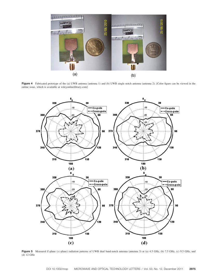
Figure 4 Fabricated prototype of the (a) UWB antenna (antenna 1) and (b) UWB single notch antenna (antenna 2). [Color figure can be viewed in the
online issue, which is available at wileyonlinelibrary.com]
Figure 5 Measured E-plane (xz-plane) radiation patterns of UWB dual band-notch antenna (antenna 3) at (a) 4.5 GHz, (b) 7.5 GHz, (c) 9.5 GHz, and
(d) 12 GHz
DOI 10.1002/mop MICROWAVE AND OPTICAL TECHNOLOGY LETTERS / Vol. 53, No. 12, December 2011 2975
However, for the other frequencies outside the notched band,
the antenna gain is appropriately consistent and almost stable in
the whole of the UWB band. The measured peak gain of UWB
dual band-notch antenna at 3.6 GHz is �15.35 dBi and at 5.4
GHz is �10.25 dBi, respectively. The top view of the fabricated
prototype of the UWB antenna (antenna 1) and single band-
notch UWB antenna (antenna 2) are shown in the Figures 4(a)
and 4(b) respectively (the bottom view of these antennas are
identical to that of antenna 3).
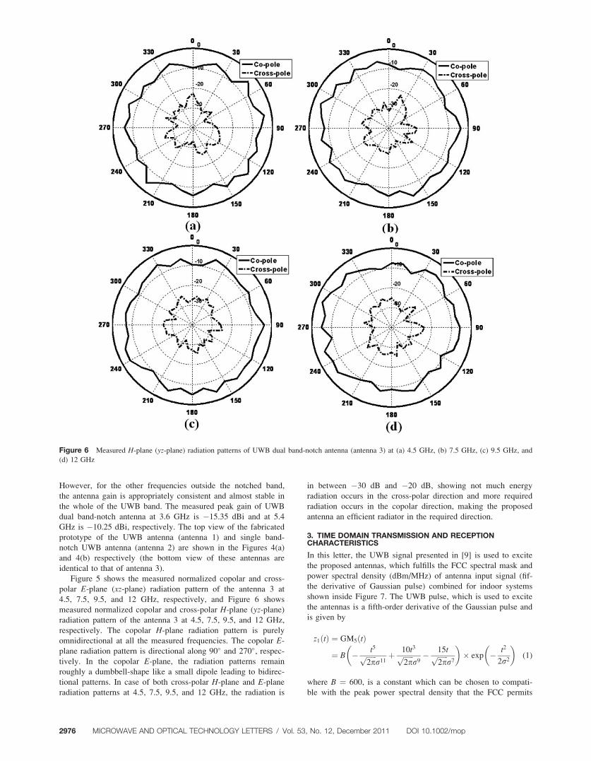
Figure 5 shows the measured normalized copolar and cross-
polar E-plane (xz-plane) radiation pattern of the antenna 3 at
4.5, 7.5, 9.5, and 12 GHz, respectively, and Figure 6 shows
measured normalized copolar and cross-polar H-plane (yz-plane)radiation pattern of the antenna 3 at 4.5, 7.5, 9.5, and 12 GHz,
respectively. The copolar H-plane radiation pattern is purely
omnidirectional at all the measured frequencies. The copolar E-plane radiation pattern is directional along 90� and 270�, respec-tively. In the copolar E-plane, the radiation patterns remain
roughly a dumbbell-shape like a small dipole leading to bidirec-
tional patterns. In case of both cross-polar H-plane and E-planeradiation patterns at 4.5, 7.5, 9.5, and 12 GHz, the radiation is
in between �30 dB and �20 dB, showing not much energy
radiation occurs in the cross-polar direction and more required
radiation occurs in the copolar direction, making the proposed
antenna an efficient radiator in the required direction.
3. TIME DOMAIN TRANSMISSION AND RECEPTIONCHARACTERISTICS
In this letter, the UWB signal presented in [9] is used to excite
the proposed antennas, which fulfills the FCC spectral mask and
power spectral density (dBm/MHz) of antenna input signal (fif-
the derivative of Gaussian pulse) combined for indoor systems
shown inside Figure 7. The UWB pulse, which is used to excite
the antennas is a fifth-order derivative of the Gaussian pulse and
is given by
z1ðtÞ ¼ GM5ðtÞ¼ B � t5ffiffiffiffiffiffi
2pp
r11þ 10t3ffiffiffiffiffiffi
2pp
r9� 15tffiffiffiffiffiffi
2pp
r7
� �� exp � t2
2r2
� �(1)
where B ¼ 600, is a constant which can be chosen to compati-
ble with the peak power spectral density that the FCC permits
Figure 6 Measured H-plane (yz-plane) radiation patterns of UWB dual band-notch antenna (antenna 3) at (a) 4.5 GHz, (b) 7.5 GHz, (c) 9.5 GHz, and
(d) 12 GHz
2976 MICROWAVE AND OPTICAL TECHNOLOGY LETTERS / Vol. 53, No. 12, December 2011 DOI 10.1002/mop

and r is the spread of Gaussian pulse, whose value is 51 ns to
ensure that the size and shape of the spectrum fit with the FCC
mask. The signal with single pulse is shown in the Figure 8.
The PSD of antenna input signal suitable fits the PSD of the
FCC mask denoting the adequate compatibility of the fifth-order
Gaussian pulse with the FCC indoor mask shown inside
Figure 7.
Figure 8(b) shows the received pulse as the antenna 3 acts as
a received antenna. The transmit antenna is also the replica of
antenna 3. That means the fifth-order Gaussian pulse is transmit-
ted from antenna 3 to antenna 3. The fifth-order Gaussian pulse
is generated in Tektronix AWG 7122B arbitrary signal generator
and it is fed to the transmit antenna 3. At 62 cm [10] away, the
receiving antenna (antenna 3) stationed face-to-face. At the
receiving side, the received signal is captured by Tektronix DPO
70804 digital phosphor oscilloscope. As from the Figure 8(b),
there is ringing in the tail of the fifth-order Gaussian pulse,
Apart from this, there is reduction in the amplitude of the
received pulse. The reason for these two types of the disturbance
in the received signal may be due to the noise and other distur-
bances present in the air channel in between the two antennas.
Similarly, Figure 8(c) shows the above characteristics when the
two antennas are place side-by-side. From Figures 8(b) and 8(c),
one can see that the ringing in the tail of the received pulse is
slightly more in case of side-by-side as compared to the ringing
present in the received signal when the antenna placed face-to-
face. This is because, when the antennas are stationed face-to-
face, the whole of the radiating surface is exposed to receiving
signal. This is the broadside direction of the radiation pattern.
Hence the signal reception is smooth in this situation. But when
the antennas are placed side-by-side, the radiation is in the end
fire direction and no radiation pattern lobes are present to cap-
ture the receiving signal. So more ringing is present in the tail
of the received signal.
4. CONCLUSIONS
To mitigate the potential interference between the UWB systems
and NB systems such as WiMAX and WLAN, an UWB PMA
with two open-circuited stubs in two sides of the microstrip
feedline for the 3.4/5.5 GHz dual-band notched characteristics
has been proposed. The relationship between the total dimension
of the two open-circuited stubs and the notch band center fre-
quency has been presented. Stable radiation pattern and constant
gain in the UWB bands are obtained. The UWB PMA presented
Figure 8 Measured received signals of antenna 3 as antenna 3 serve as the receiving antennas with single pulse input signal (a) transmitted Gaussian
pulse, (b) antenna 3 face-to-face, and (c) antenna 3 side-by-side
Figure 7 Antenna input signal (fifth derivative of Gaussian pulse)
with single pulse
DOI 10.1002/mop MICROWAVE AND OPTICAL TECHNOLOGY LETTERS / Vol. 53, No. 12, December 2011 2977

in this letter is expected to find future applications in UWB sys-
tems for coexistence with the NB systems.
ACKNOWLEDGMENTS
The authors thank U. K. Sarma and D. Goswami of IIT Guwahati,
G. Hemanth and Hemalatha of IISc Bangalore for their assistance
in fabrication and measurements of the proposed antennas. Second
author is grateful to Dr. K. J. Vinoy of IISc Bangalore and Prof. A.
Mahanta of IIT Guwahati for allowing the first author to use their
laboratories for various measurements of the proposed antennas.
REFERENCES
1. First Report and Order, Revision of Part 15 of the Commission’s
Rule Regarding Ultra-Wideband Transmission systems FCC 02–48,
Federal Communication Commission, 2002.
2. R. Zaker, C. Ghobadi, and J. Nourinia, Novel modified UWB pla-
nar monopole antenna with variable frequency band-notch function,
IEEE Antenna Wireless Propagat Lett 7 (2008), 112–114.
3. J. Liu, S. Gong, Y. Ku, X. Zhang, C. Feng, and N. Qi, Compact
printed ultra-wideband monopole antenna with dual band-notched
characteristics, Electron Lett 44 (2008), 710–711.
4. H. Lee, Y. Jang, J. Kim, and J. Choi, Wideband monopole antenna
with WLAN (2.4 GHz/5 GHz) dual band-stop function, Microwave
Opt Technol Lett 50 (2008), 1646–1649.
5. F.-J. Wang, X.-X. Yang, J.-S. Zhang, G.-P. Guo, and J.-X. Xiao, A
band-notched ring monopole antenna, Microwave Opt Technol Lett
50 (2008), 1882–1884.
6. Z. Cui, Y.-C. Jiao, L. Zhang, and F.-S. Zhang, The band-notch
function for a printed ultra-wideband monopole antenna with
E-shaped slot, Microwave Opt Technol Lett 50 (2008), 2048–2052.
7. Y.-D. Dong, W. Hong, Z.-Q. Kuai, and J.-X. Chen, Analysis of
planar ultrawideband antennas with on-ground slot band-notched
structures, IEEE Trans Antennas Propagat 57 (2009), 1886–1892.
8. IE3D version 10.2, Zeland Corp., Freemont, CA, USA.
9. H. Kim, D. Park, and Y. Joo, All-digital low power CMOS pulse
generator for UWB signals, Electron Lett 40 (2004), 1534–1535.
10. N. Telzhensky and Y. Leviatan, Novel method of UWB antenna
optimization for specified input signal form by means of genetic
algorithm, IEEE Trans Antennas Propagat 54 (2006), 2216–2225.
VC 2011 Wiley Periodicals, Inc.
INVESTIGATION OF AN ULTRA-WIDEBAND MICROSTRIP ANTENNAUSING FINITE ELEMENTARY LINESAPPROACH
S. Senouci,1 A. Zerguerras,2 J. Tao,2 and T. H. Vuong2
1 Departement d’Electronique, Ecole Nationale Polytechnique,Alger, Algerie2 Laboratoire LAPLACE, ENSEEIHT-INP, Toulouse, France;Corresponding author: [email protected] [email protected]
Received 8 March 2011
ABSTRACT: This work presents an investigation, using the approach offinite elementary lines (FEL), of an ultra-wideband antenna. Two ways for
expanding frequency band were combined: the electromagnetic couplingand the insertion of an air layer. A prototype of this antenna has beenrealized. A comparison between the antenna performance predicted by our
approach and those provided by the high-frequency simulation structure(HFSS) software and those measured is presented. An impedance
bandwidth of about 50% and directivity at the first resonance of about 9 dBwere achieved. A satisfactory concordance between results of our approachand measures is observed. The novelty of this work lies in the treatment by
the FEL method, for the first time, of singularities induced by the gap of
coupling and the jump of width. The computing time consumed by the FELapproach is about 10 times less than that consumed by the HFSS software
to analyze the same structure on the same number of point’s frequencydomain, the latter being 68 min.VC 2011 Wiley Periodicals, Inc. Microwave
Opt Technol Lett 53:2978–2985, 2011; View this article online at
wileyonlinelibrary.com. DOI 10.1002/mop.26379
Key words: microstrip antennas; band expanding techniques; coupling;electromagnetic; coupling gap; width jump
1. INTRODUCTION
The ultra-wideband (UWB) systems are defined as systems that
use signals with bandwidths exceeding 500 MHz or a bandwidth
of 20% around its central frequency. UWB systems provide
higher rates for wireless communications, radar systems, and
precise geo-location. The mistress component of these systems
is the UWB antenna.
The microstrip antennas are usually based driver patch
printed on a microwave dielectric substrate having a face com-
pletely covered with conductive metal, called ground plane.
These antennas have several advantages such as low profile, low
cost, light weight, easy fabrication, and conformability on
curved surfaces. However, their major drawbacks are the small
gain and the close frequency bandwidth, because in practice
applications-based microstrip antennas require high gain and
wide frequency bands.
Indeed, miniaturization of microstrip antennas, extending
their frequency bands and increase their gains are operations
required for some practical applications such as mobile cell
phone wireless, direct broadcast satellite, the wireless LAN, sat-
ellite global positioning, and other future generations of wireless
terminals.
These three operations are changing in meaning contradic-
tory, that is to say, the miniaturization leads to a drop in gain
and increase the gain adversely affects the band width; this leads
to seek a compromise between the parameters of the antenna to
achieve the desired performance for a specific application.
Widening the frequency band of a microstrip plate antenna
(MPA) calls the use of substrates with low dielectric constant
and high thickness [1–6]. But the excessive increase in thickness
to improve bandwidth causes unwanted radiation and increases
the power of surface waves contributing to the decrease in
antenna efficiency. Therefore, a compromise between the dielec-
tric constant, the thickness of the substrate and the bandwidth is
taken into account during the synthesis of MPA.
The physical dimensions of the antenna are an important
factor in the design process [7] to which is due the miniaturi-
zation of modern mobile phones. Much attention has been
given to a technique for miniaturizing the dimensions of the
MPA [8–12]. The electrical requirements of these mobile
antennas are sufficient bandwidth, high efficiency, impedance
matching, omnidirectional radiation patterns, and minimal deg-
radation by the presence of objects in the immediate vicinity,
and so on.
The bandwidth enlargement technique used in this letter is
one that combines both techniques simultaneously, namely: first,
the electromagnetic coupling between a patch excited by coaxial
probe called driven patch and a patch coplanar with the first
known as parasitic patch or director patch. A first enlargement
is obtained by the juxtaposition of the two resonances of the
two patches. The second technique is the inclusion of a layer of
air between the ground plane and the substrate. The air layer
2978 MICROWAVE AND OPTICAL TECHNOLOGY LETTERS / Vol. 53, No. 12, December 2011 DOI 10.1002/mop