Embed Size (px)
Citation preview
iMX7 Dual COM Board - Datasheet Copyright 2018 © Embedded Artists AB
EA2-USG-1603 Rev A
Document status: Preliminary
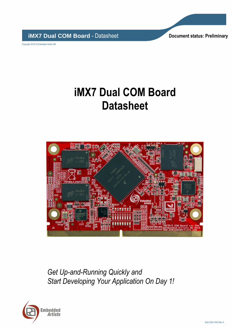
iMX7 Dual COM Board Datasheet
Get Up-and-Running Quickly and Start Developing Your Application On Day 1!

iMX7 Dual COM Board - Datasheet Page 2
Copyright 2018 © Embedded Artists AB
Embedded Artists AB Davidshallsgatan 16 211 45 Malmö Sweden
http://www.EmbeddedArtists.com
Copyright 2018 © Embedded Artists AB. All rights reserved.
No part of this publication may be reproduced, transmitted, transcribed, stored in a retrieval system, or translated into any language or computer language, in any form or by any means, electronic, mechanical, magnetic, optical, chemical, manual or otherwise, without the prior written permission of Embedded Artists AB.
Disclaimer
Embedded Artists AB makes no representation or warranties with respect to the contents hereof and specifically disclaim any implied warranties or merchantability or fitness for any particular purpose. The information has been carefully checked and is believed to be accurate, however, no responsibility is assumed for inaccuracies. Information in this publication is subject to change without notice and does not represent a commitment on the part of Embedded Artists AB.
Feedback
We appreciate any feedback you may have for improvements on this document.
Trademarks
All brand and product names mentioned herein are trademarks, services marks, registered trademarks, or registered service marks of their respective owners and should be treated as such.

iMX7 Dual COM Board - Datasheet Page 3
Copyright 2018 © Embedded Artists AB
Table of Contents 1 Document Revision History 5
2 Introduction 6
2.1 Hardware 6
2.2 Software 7
2.3 Features and Functionality 7
2.4 Interface Overview 9
2.5 Reference Documents 10
3 Board Pinning 12
3.1 Pin Numbering 12
3.2 Pin Assignment 13
4 Pin Mapping 23
4.1 Functional Multiplexing on I/O Pins 23
4.1.1 Alternative I/O Function List 23
4.2 I/O Pin Control 23
5 Interface Description 24
5.1 Camera Interfaces 25
5.1.1 Parallel Camera Interface 25
5.1.2 Serial Camera Interface 28
5.2 Display Interfaces 29
5.2.1 Parallel RGB LCD Interface 30
5.2.2 MIPI-DSI Interface 31
5.3 Digital Audio Interfaces: Synchronous Audio Interfaces (SAI) 32
5.4 Digital Audio Interface: Medium Quality Speaker (MQS) 34
5.5 Ethernet 35
5.5.1 Second Ethernet Interface 36
5.6 FlexCAN 38
5.7 GPIOs 38
5.8 I2C 39
5.9 JTAG 41
5.10 PCI Express 42
5.11 Power Management 42
5.12 Power Supply Signals 43
5.13 PWM 43
5.14 SD/MMC 44
5.15 ECSPI / SPI 46
5.16 UART 47
5.17 USB 50
6 Boot Options 52

iMX7 Dual COM Board - Datasheet Page 4
Copyright 2018 © Embedded Artists AB
7 Power Modes 54
7.1 Power Mode: OFF 55
7.2 Power Mode: SNVS (RTC only) 55
7.3 Power Mode: LPSR 55
7.4 Power Modes: Low Power 55
7.5 Power Mode: RUN 56
8 Technical Specification 57
8.1 Absolute Maximum Ratings 57
8.2 Recommended Operating Conditions 57
8.3 Power Ramp-Up Time Requirements 57
8.4 Electrical Characteristics 57
8.4.1 Reset Output Voltage Range 57
8.4.2 Reset Input 58
8.5 Power Consumption 58
8.6 Mechanical Dimensions 58
8.6.1 MXM3 Socket 60
8.6.2 Module Assembly Hardware 60
8.7 Environmental Specification 61
8.7.1 Operating Temperature 61
8.7.2 Relative Humidity (RH) 61
8.8 Thermal Design Considerations 61
8.8.1 Thermal Parameters 61
8.9 Product Compliance 62
9 Functional Verification and RMA 63
10 Things to Note 64
10.1 Shared Pins and Multiplexing 64
10.2 Cannot Access Some Memory Cards 64
10.3 Only Use EA Board Support Package (BSP) 65
10.4 OTP Fuse Programming 65
10.5 Write Protect on Parameter Storage E2PROM 65
10.6 Integration - Contact Embedded Artists 65
10.7 ESD Precaution when Handling iMX7 Dual COM Board 66
10.8 EMC / ESD 66
11 Custom Design 68
12 Disclaimers 69
12.1 Definition of Document Status 70

iMX7 Dual COM Board - Datasheet Page 5
Copyright 2018 © Embedded Artists AB
1 Document Revision History
Revision Date Description
PA1 2016-10-24 First version.
PA2 2016-11-21 Added information about how to connect an external Ethernet PHY.
PA3 2017-07-31 Added information about boot control pins.
PA4 2018-03-14 Added information about current consumption.

iMX7 Dual COM Board - Datasheet Page 6
Copyright 2018 © Embedded Artists AB
2 Introduction This document is a datasheet that specifies and describes the iMX7 Dual COM Board mainly from a hardware point of view. Some basic software related issues are also addressed, like booting and functional verification, but there are separate software development manuals that should also be consulted.
2.1 Hardware
The iMX7 Dual COM Board is a Computer-on-Module (COM) based on NXP's dual-core ARM Cortex-A7 / M4 i.MX 7Dual System-on-Chip (SoC) application processor. The board provides a quick and easy solution for implementing a high-performance ARM dual-core Cortex-A7 / M4 based design. The two Cortex-A7 cores runs at up to 1GHz and the Cortex-M4 core at up to 200 MHz.
The heterogeneous core architecture enables the system to run an OS like Linux on the two Cortex-A7 cores and a Real-Time OS (RTOS) on the Cortex-M4. This architecture is ideal for real time applications where Linux cannot be used for all time critical task. The Cortex-M4 can handle (real time) critical tasks and can also be used to lower the power consumption.
The iMX7 Dual COM Board delivers high computational and graphical performance at very low power consumption. The on-board PMIC, supporting DVFS (Dynamic Voltage and Frequency Scaling), together with a LPDDR3 memory sub-system reduce the power consumption to a minimum.
The SoC is part of the scalable i.MX 6/7 product family. There is a range of i.MX 6/7 COM Boards from Embedded Artists with single, dual and quad Cortex-A9/A7 cores, with or without a heterogeneous Cortex-M4 core. All boards share the same basic pinning for maximum flexibility and performance scalability.
The iMX7 Dual COM Board has a very small form factor and shields the user from a lot of complexity of designing a high performance system. It is a robust and proven design that allows the user to focus the product development, shorten time to market and minimize the development risk.
The iMX7 Dual COM Board targets a wide range of applications, such as:
Portable systems
HMI/GUI solutions
Portable medical and health care
Connected vending machines
Point-of-Sale (POS) applications
Access control panels
Audio
IP phones
Smart appliances
eReaders
Wearables
Home energy management systems
Industrial automation
HVAC Building and Control Systems
Smart Grid and Smart Metering
Smart Toll Systems
Data acquisition
Communication gateway solutions
Connected real-time systems
...and much more
The picture below illustrates the block diagram of the iMX7 Dual COM Board.

iMX7 Dual COM Board - Datasheet Page 7
Copyright 2016 © Embedded Artists AB
Figure 1 – iMX7 Dual COM Board Block Diagram
The iMX7 Dual COM Board pin assignment focus on direct connection to (carrier board) interface connectors and minimize trace and layer crossing. This is important for high speed, serial interfaces with impedance controlled differential pairs. As a result, carrier boards can be designed with few routing layers. In many cases, a four layer pcb is enough to implement advanced and compact carrier boards. The pin assignment is common for the iMX6/7 COM Boards from Embedded Artists and the general, so called, EACOM specification is found in separate document.
2.2 Software
The iMX7 Dual COM Board has Board Support Packages (BSPs) for Embedded Linux and Android. Precompiled images are available. Embedded Artists works with partners that can provide support for other operating systems (OS). For more information contact Embedded Artists support.
This document has a hardware focus and does not cover software development. See other documents related to the iMX7 Dual COM Board for more information about software development.
2.3 Features and Functionality
The i.MX 7Dual is a powerful SoC. The full specification can be found in NXP's i.MX 7Dual Datasheet and i.MX 7Dual Reference Manual. The table below lists the main features and functions of the iMX7 Dual COM board - which represents Embedded Artists integration of the i.MX 7Dual SoC. Due to pin configuration some functions and interfaces of the i.MX7 Dual many not be available at the same time. See i.MX 7Dual SoC datasheet and reference manual for details. Also see pin multiplexing Excel sheet for details.
Group Feature iMX7 Dual COM Board
CPUs NXP SoC commercial temperature range industrial temperature range
MCIMX7D7DVM10S (0 - 60° C) MCIMX7D5EVM10S (-20 - 85° C)
CPU Cores 2x Cortex-A7 1x Cortex-M4 with MPU/FPU
L1 Instruction cache 32 KByte for each Cortex-A7
NXP i.MX 7Dual with dual-core ARM
Cortex-A7 / Cortex-M4 @ 1 GHz / 200 MHz
DDR3L Memory (32 bit data bus)
PMIC 3.3V input
QSPI Flash
I2C#0
MXM3 connector (314 pins)
10/100/1000 Mbps
Ethernet-PHY
eMMC Flash
JTAG connector
Parameter storage
SD3
QSPIA
Boot control

iMX7 Dual COM Board - Datasheet Page 8
Copyright 2016 © Embedded Artists AB
16 KByte on Cortex-M4
L1 Data cache 32 KByte for each Cortex-A7 16 KByte on Cortex-M4
L2 Cache on Cortex-A7 cores 512 KByte
TCM on Cortex-M4 64 KByte
NEON SIMD media accelerator on Cortex-A7
Maximum CPU frequency 996 MHz on Cortex-A7 200 MHz on Cortex-M4
Security Functions
ARM TrustZone
Advanced High Assurance Boot
Cryptographic Acceleration and Assurance Module
Secure Non-Volatile Storage,
System JTAG controller
Memory DDR3L RAM Size 1 GByte
DDR3L RAM Speed 1066 MT/s
DDR3L RAM Memory Width 32 bit
QSPI Memory 32 MByte
eMMC NAND Flash (8 bit) 4 GByte
Graphical Processing
PiXel Processing Pipeline (PXP)
Graphical Output
RGB, 24-bit parallel interface
MIPI-DSI, 2 lanes
EPD
LVDS Optional MIPI-DSI to LVDS bridge
Graphical Input
Parallel camera, up to 24-bit parallel interface
MIPI-CSI, 2 lanes
Interfaces (all functions are not available at the same time)
Dual 10/100/1000 Mbps Gigabit Ethernet controllers (IEEE1588 compliant) with support for Audio Video Bridging (AVB)
with on-board PHY Note: off-board PHYs required for second port
Quad SPI QSPIA interface used on-board
PCIe v2.1 (1 lane)
8 ch 12-bit ADC
2x USB 2.0 OTG ports, 1x HSIC
3x SD3.0/MMC 5.0 SD3 interface used on-board to eMMC
4x SPI, 7x UART, 4x I²C, 3x I²S/AC97

iMX7 Dual COM Board - Datasheet Page 9
Copyright 2016 © Embedded Artists AB
Dual FlexCAN, CAN bus 2.0B
4x PWM, KPP, GPIOs, WDOG
Other PMIC (PF3000) supporting DVFS techniques for low power modes
E2PROM storing board information including Ethernet MAC address and memory bus setup parameters
i.MX7 Dual on-chip RTC
On-board watchdog functionality
2.4 Interface Overview
The table below lists the interfaces that are specified in the EACOM specification (see separate document for details) and what is supported by the iMX7 Dual COM board.
Interface EACOM specification iMX7 Dual COM Board
Note
UART 3 ports (two 4 wire and one 2 wire)
3 ports More ports available as alternative pin functions
SPI 2 ports 2 port More ports available as alternative pin functions
I2C 3 ports 3 ports A fourth port is available as alternative pin functions
SD/MMC 2 ports (one 4 databits and one 8 databits)
2 ports Both ports have 4 databits
Parallel LCD 24 databits and CLK/HS/VS/DE
Full support
LCD support LCD power ctrl, Backlight power/contrast control, touch panel ctrl (RST and IRQ)
Full support 1 PWM and 4 GPIO
LVDS LCD 2 ports (18/24 bit LVDS data) - Optional support with MIPI-DSI to LVDS bridge
HDMI (TDMS) -
Parallel Camera -
Serial Camera CSI, 4 lane 2 lanes supported
Gigabit Ethernet 2 ports 1 ports Second port via external Eth-Phy
PCIe 1 post, 1 lane 1 port, 1 lane
SATA 1 port -
USB 1 USB3.0 OTG 1 USB3.0 Host 1 USB2.0 Host
2 USB2.0 OTG

iMX7 Dual COM Board - Datasheet Page 10
Copyright 2016 © Embedded Artists AB
SPDIF 1 TX/RX port -
CAN 2 ports 2 ports
I2S/SSI/AC97 1 port (4 wire synchronous plus MCLK)
1 port More ports available as alternative pin functions.
Analog audio Stereo output -
GPIO 9 pins 9 pins More GPIO pins are available as alternative pin functions.
PWM 1 pin 1 pin More pins are available as alternative pin functions.
ADC 8 inputs 8 inputs Note: max 1.8V input
Type specific 39 pins 33 pins, incl MIPI-DSI port
All type specific pins connected to i.MX 7Dual pins.
6 type specific pins not used since all i.MX 7Dual SoC pins allocated.
Power 10 VIN, VBAT and 47 GND 10 VIN, VBAT and 47 GND
About 15% of the pins are ground pins.
2.5 Reference Documents
The following documents are important reference documents and should be consulted when integrating the iMX7 Dual COM board:
EACOM Board Specification
EACOM Board Integration Manual
The following NXP documents are also important reference documents and should be consulted for functional details:
IMX7DCEC, i.MX 7Dual Applications Processors for Consumer Products - Data Sheet, latest revision
IMX7DRM, i.MX 7Dual Applications Processor Reference Manual, latest revision
IMX7DCE, Chip Errata for the i.MX 7Dual, latest revision Note: It is the user's responsibility to make sure all errata published by the manufacturer are taken note of. The manufacturer's advice should be followed.
i.MX 7Dual Power Consumption Measurement, latest revision
AN5334, i.MX7 Dual/Solo Product Lifetime Usage Estimates, latest revision
The following documents are external industry standard reference documents and should also be consulted when applicable:

iMX7 Dual COM Board - Datasheet Page 11
Copyright 2016 © Embedded Artists AB
eMMC (Embedded Multi-Media Card) the eMMC electrical standard is defined by JEDEC JESD84-B45 and the mechanical standard by JESD84-C44 (www.jedec.org)
GbE MDI (Gigabit Ethernet Medium Dependent Interface) defined by IEEE 802.3. The 1000Base-T operation over copper twisted pair cabling is defined by IEEE 802.3ab (www.ieee.org)
The I2C Specification, Version 2.1, January 2000, Philips Semiconductor (now NXP) (www.nxp.com)
I2S Bus Specification, Feb. 1986 and Revised June 5, 1996, Philips Semiconductor (now NXP) (www.nxp.com)
JTAG (Joint Test Action Group) defined by IEEE 1149.1-2001 - IEEE Standard Test Access Port and Boundary Scan Architecture (www.ieee.org)
MXM3 Graphics Module Mobile PCI Express Module Electromechanical Specification, Version 3.0, Revision 1.1, © 2009 NVIDIA Corporation (www.mxm-sig.org)
PCI Express Specifications (www.pci-sig.org)
SD Specifications Part 1 Physical Layer Simplified Specification, Version 3.01, May 18, 2010, © 2010 SD Group and SD Card Association (Secure Digital) (www.sdcard.org)
SPI Bus – “Serial Peripheral Interface” – de-facto serial interface standard defined by Motorola. A good description may be found on Wikipedia (http://en.wikipedia.org/wiki/Serial_Peripheral_Interface_Bus)
DSI (Display Serial Interface) The DSI standard is owned and maintained by the MIPI Alliance (“Mobile Industry Processor Alliance”) (www.mipi.org)
CSI-2 (Camera Serial Interface version 2) The CSI-2 standard is owned and maintained by the MIPI Alliance (“Mobile Industry Processor Alliance”) (www.mipi.org)
USB Specifications (www.usb.org)

iMX7 Dual COM Board - Datasheet Page 12
Copyright 2016 © Embedded Artists AB
3 Board Pinning Embedded Artists has created the EACOM Board Specification that is based on the SMARC form factor; module size 82 x 50 mm. Note that pinning is different from the SMARC standard. See the EACOM Board specification document for details and background information. Hereafter this standard will be referred to as EACOM.
The carrier board connector has 314 pins with 0.5 mm pitch and the EACOM board is inserted in a right angle (R/A) style. The connector is originally defined for use with MXM3 graphics cards. There are multiple sources for carrier board (MXM3) connectors due to the popular standard. The signal integrity is excellent and suitable for data rates up to 5 GHz.
Overall assembly height of the EACOM board/Carrier board connector can be as low as 6 mm. There are different stack height options available, including 2.7 mm (resulting in overall 6 mm height), 5 mm and 8 mm.
3.1 Pin Numbering
The figures below show the pin numbering for EACOM. Top side edge fingers are numbered P1-P156. Bottom side edge fingers are numbered S1-S158. There is an alternative pin numbering that follows the MXM3 standard with even numbers on the bottom and odd numbers on the top. This numbering is from 1-321, with 7 numbers/pins (150-156) removed due to the keying.
Figure 2 – EACOM Board Pin Numbering, Top Side
P1/2 P156/320

iMX7 Dual COM Board - Datasheet Page 13
Copyright 2016 © Embedded Artists AB
Figure 3 – EACOM Board Pin Numbering, Bottom Side
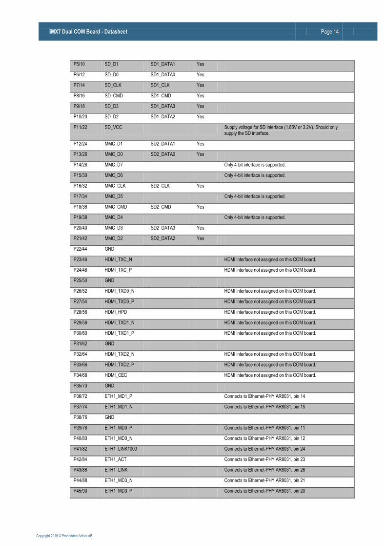
3.2 Pin Assignment
This section describes the pin assignment of the board, with the following columns:
Pin number Px are top side edge fingers. Sx are bottom side edge fingers. An alternative, consecutive, numbering is also shown with odd numbers on the top and even numbers on the bottom side.
EACOM Board Describe the typical usage of the pin according to EACOM. This pin usage should be followed to get compatibility between different EACOM boards. If this is not needed, then any of the alternative functions on the pin can also be used.
i.MX 7Dual Ball Name The name of the ball of the i.MX 7Dual SoC (or other component on the EACOM board) that is connected to this pin.
Notes When relevant, the preferred pin function is listed.
There are 47 ground pins, which equal to about 15%, and 10 input voltage supply pins.
Note that some pins are EACOM board type specific, meaning that these pins might not be compatible with other EACOM boards. Using these may result in lost compatibility between EACOM boards, but not always. Check details between EACOM boards of interest.
The table below lists the top side pins, P1-P156, odd numbers.
Top Side Pin Number
EACOM Board i.MX 7Dual Ball Name
Alternative pin functions?
Notes
P1/2 GPIO6 EPDC_SDCE3 Yes GPIO6 controlled by alternative pin function GPIO2_IO23
P2/4 GPIO5 EPDC_SDCE2 Yes GPIO5 controlled by alternative pin function GPIO2_IO22
P3/6 GPIO4 SD1_CD Yes GPIO4 controlled by alternative pin function GPIO5_IO01
P4/8 GPIO3 SD1_RESET Yes GPIO3 controlled by alternative pin function GPIO5_IO02
S158/321 S1/1
iMX7 Dual COM Board - Datasheet Page 14
Copyright 2016 © Embedded Artists AB
P5/10 SD_D1 SD1_DATA1 Yes
P6/12 SD_D0 SD1_DATA0 Yes
P7/14 SD_CLK SD1_CLK Yes
P8/16 SD_CMD SD1_CMD Yes
P9/18 SD_D3 SD1_DATA3 Yes
P10/20 SD_D2 SD1_DATA2 Yes
P11/22 SD_VCC Supply voltage for SD interface (1.85V or 3.2V). Should only supply the SD interface.
P12/24 MMC_D1 SD2_DATA1 Yes
P13/26 MMC_D0 SD2_DATA0 Yes
P14/28 MMC_D7 Only 4-bit interface is supported.
P15/30 MMC_D6 Only 4-bit interface is supported.
P16/32 MMC_CLK SD2_CLK Yes
P17/34 MMC_D5 Only 4-bit interface is supported.
P18/36 MMC_CMD SD2_CMD Yes
P19/38 MMC_D4 Only 4-bit interface is supported.
P20/40 MMC_D3 SD2_DATA3 Yes
P21/42 MMC_D2 SD2_DATA2 Yes
P22/44 GND
P23/46 HDMI_TXC_N HDMI interface not assigned on this COM board.
P24/48 HDMI_TXC_P HDMI interface not assigned on this COM board.
P25/50 GND
P26/52 HDMI_TXD0_N HDMI interface not assigned on this COM board.
P27/54 HDMI_TXD0_P HDMI interface not assigned on this COM board.
P28/56 HDMI_HPD HDMI interface not assigned on this COM board.
P29/58 HDMI_TXD1_N HDMI interface not assigned on this COM board.
P30/60 HDMI_TXD1_P HDMI interface not assigned on this COM board.
P31/62 GND
P32/64 HDMI_TXD2_N HDMI interface not assigned on this COM board.
P33/66 HDMI_TXD2_P HDMI interface not assigned on this COM board.
P34/68 HDMI_CEC HDMI interface not assigned on this COM board.
P35/70 GND
P36/72 ETH1_MD1_P Connects to Ethernet-PHY AR8031, pin 14
P37/74 ETH1_MD1_N Connects to Ethernet-PHY AR8031, pin 15
P38/76 GND
P39/78 ETH1_MD0_P Connects to Ethernet-PHY AR8031, pin 11
P40/80 ETH1_MD0_N Connects to Ethernet-PHY AR8031, pin 12
P41/82 ETH1_LINK1000 Connects to Ethernet-PHY AR8031, pin 24
P42/84 ETH1_ACT Connects to Ethernet-PHY AR8031, pin 23
P43/86 ETH1_LINK Connects to Ethernet-PHY AR8031, pin 26
P44/88 ETH1_MD3_N Connects to Ethernet-PHY AR8031, pin 21
P45/90 ETH1_MD3_P Connects to Ethernet-PHY AR8031, pin 20

iMX7 Dual COM Board - Datasheet Page 15
Copyright 2016 © Embedded Artists AB
P46/92 GND
P47/94 ETH1_MD2_N Connects to Ethernet-PHY AR8031, pin 18
P48/96 ETH1_MD2_P Connects to Ethernet-PHY AR8031, pin 17
P49/98 GND
P50/100 ETH2_MD1_P
P51/102 ETH2_MD1_N
P52/104 GND
P53/106 ETH2_MD0_P
P54/108 ETH2_MD0_N
P55/110 ETH2_LINK1000
P56/112 ETH2_ACT
P57/114 ETH2_LINK
P58/116 ETH2_MD3_N
P59/118 ETH2_MD3_P
P60/120 GND
P61/122 ETH2_MD2_N
P62/124 ETH2_MD2_P
P63/126 GND
P64/128 USB_O1_DN USB_OTG1_DN No
P65/130 USB_O1_DP USB_OTG1_DP No
P66/132 USB_O1_OTG_ID USB_OTG1_ID No
P67/134 USB_O1_SSTXN USB OTG port #1 on i.MX 7Dual does not support USB 3.0 so this pin is unconnected.
P68/136 USB_O1_SSTXP USB OTG port #1 on i.MX 7Dual does not support USB 3.0 so this pin is unconnected.
P69/138 GND
P70/140 USB_O1_SSRXN USB OTG port #1 on i.MX 7Dual does not support USB 3.0 so this pin is unconnected.
P71/142 USB_O1_SSRXP USB OTG port #1 on i.MX 7Dual does not support USB 3.0 so this pin is unconnected.
P72/144 USB_O1_VBUS USB_OTG1_VBUS No
P73/146 USB_O1_PWR_EN GPIO1_IO05 Yes Controlled by alternative pin function USB_OTG1_PWR
P74/148 USB_O1_OC GPIO1_IO04 Yes Controlled by alternative pin function USB_OTG1_OC
150 Non existing pin
152 Non existing pin
154 Non existing pin
156 Non existing pin
P75/158 USB_H1_PWR_EN GPIO1_IO07 Yes Controlled by alternative pin function USB_OTG2_OC
P76/160 USB_H1_OC GPIO1_IO06 Yes Controlled by alternative pin function USB_OTG2_PWR
P77/162 GND
P78/164 USB_H1_DN USB_OTG2_DN No
P79/166 USB_H1_DP USB_OTG2_DP No
P80/168 USB_H1_SSTXN USB OTG port #2 on i.MX 7Dual does not support USB 3.0 so this pin is unconnected.

iMX7 Dual COM Board - Datasheet Page 16
Copyright 2016 © Embedded Artists AB
P81/170 USB_H1_SSTXP USB_OTG2_ID No USB OTG port #2 on i.MX 7Dual does not support USB 3.0.
Non-standard pin allocation.
P82/172 GND
P83/174 USB_H1_SSRXN SNVS_TAMPER2 No USB OTG port #2 on i.MX 7Dual does not support USB 3.0.
Non-standard pin allocation.
P84/176 USB_H1_SSRXP SNVS_TAMPER1 No USB OTG port #2 on i.MX 7Dual does not support USB 3.0.
Non-standard pin allocation.
P85/178 USB_H1_VBUS USB_OTG2_VBUS No
P86/180 USB_H2_PWR_EN SNVS_TAMPER0 No USB Host port #2 on i.MX 7Dual does not exist.
Non-standard pin allocation.
P87/182 USB_H2_OC ONOFF No USB Host port #2 on i.MX 7Dual does not exist.
Non-standard pin allocation.
P88/184 GND
P89/186 USB_H2_DN HSIC_STROBE No USB Host port #2 on i.MX 7Dual does not exist.
Non-standard pin allocation.
P90/188 USB_H2_DP HSIC_DATA No USB Host port #2 on i.MX 7Dual does not exist.
Non-standard pin allocation.
P91/190 GND
P92/192 COM board specific EPDC_PWRSTAT Yes
P93/194 COM board specific EPDC_PWRCOM Yes
P94/196 COM board specific EPDC_SDOE Yes
P95/198 COM board specific EPDC_SDLE Yes
P96/200 COM board specific EPDC_SDCLK Yes
P97/202 COM board specific EPDC_D15 Yes
P98/204 COM board specific EPDC_D14 Yes
P99/206 COM board specific EPDC_D13 Yes
P100/208 COM board specific EPDC_D12 Yes
P101/210 COM board specific EPDC_D11 Yes
P102/212 COM board specific EPDC_D10 Yes
P103/214 COM board specific EPDC_D9 Yes
P104/216 COM board specific EPDC_D8 Yes
P105/218 COM board specific EPDC_D7 Yes
P106/220 COM board specific
P107/222 COM board specific
P108/224 COM board specific EPDC_D4 Yes
P109/226 COM board specific
P110/228 COM board specific
P111/230 COM board specific
P112/232 COM board specific
P113/234 COM board specific UART3_CTS Yes
P114/236 COM board specific EPDC_BDR1 Yes
P115/238 COM board specific EPDC_BDR0 Yes

iMX7 Dual COM Board - Datasheet Page 17
Copyright 2016 © Embedded Artists AB
P116/240 COM board specific UART3_RTS Yes
P117/242 COM board specific GPIO1_IO08 Yes Signal can be used on control voltage level of SD_VCC (3.3V or 1.8V). If this functionality is no needed the pin can be used freely.
P118/244 GND
P119/246 SPI-B_SSEL ECSPI2_SS0 Yes Controlled by alternative pin function ECSPI2_SS0
P120/248 SPI-B_MOSI ECSPI2_MOSI Yes Controlled by alternative pin function ECSPI2_MOSI
P121/250 SPI-B_MISO ECSPI2_MISO Yes Controlled by alternative pin function ECSPI2_MISO
P122/252 SPI-B_CLK ECSPI2_SCLK Yes Controlled by alternative pin function ECSPI2_SCLK
P123/254 SPI-A_SSEL ECSPI1_SS0 Yes Controlled by alternative pin function ECSPI1_SS0
P124/256 SPI-A_MOSI ECSPI1_MOSI Yes Controlled by alternative pin function ECSPI1_MOSI
P125/258 SPI-A_MISO ECSPI1_MISO Yes Controlled by alternative pin function ECSPI1_MISO
P126/260 SPI-A_CLK ECSPI1_SCLK Yes Controlled by alternative pin function ECSPI1_SCLK
P127/262 GND
P128/264 UART-C_RXD UART3_RXD Yes Controlled by alternative pin function UART3_RXD
P129/266 UART-C_TXD UART3_TXD Yes Controlled by alternative pin function UART3_TXD
P130/268 UART-B_RXD UART2_RXD Yes Controlled by alternative pin function UART2_RXD
P131/270 UART-B_CTS SAI2_RXD Yes Controlled by alternative pin function UART2_CTS_B
P132/272 UART-B_RTS SAI2_TXD Yes Controlled by alternative pin function UART2_RTS_B
P133/274 UART-B_TXD UART2_TXD Yes Controlled by alternative pin function UART2_TXD
P134/276 UART-A_RXD UART1_TXD Yes Controlled by alternative pin function UART1_RXD
P135/278 UART-A_CTS SAI2_TXFS Yes Controlled by alternative pin function UART1_CTS_B
P136/280 UART-A_RTS SAI2_TXC Yes Controlled by alternative pin function UART1_RTS_B
P137/282 UART.A_TXD UART1_TXD Yes Controlled by alternative pin function UART1_TXD
P138/284 PWM GPIO1_IO03 Yes Controlled by alternative pin function PWM3_OUT. Pin can only be an output since signal pass through a voltage level translator.
P139/286 GPIO2 EPDC_SDCE1 Yes GPIO2 controlled by alternative pin function GPIO2_IO21
P140/288 GPIO1 EPDC_SDCE0 Yes GPIO1 controlled by alternative pin function GPIO2_IO20
P141/290 PERI_PWR_EN RESET_OUT Yes Enable signal (active high) for carrier board peripheral power supplies. More information about carrier board design can be found in EACOM Board specification.
This signal is a copy of the RESET_OUT signal.
P142/292 RESET_IN Reset input, active low. Pull signal low to activate reset. No need to pull signal high externally.
P143/294 RESET_OUT Reset (open drain) output, active low. Driven low during reset. 1.5K pull-up resistor to VIN.
P144/296 GND
P145/298 VBAT Supply voltage from coin cell battery for keeping PMIC and RTC functioning during standby.
P146/300 E2PROM_WP Should be left open (will write protect the on-board parameter storage E2PROM), or connected to GND (will enable writes to the on-board parameter storage E2PROM AND place the i.MX 7Dual SoC in USB OTG boot mode after a power cycle).
P147/302 VIN Main input voltage supply (3.3V)
P148/304 VIN Main input voltage supply (3.3V)
P149/306 VIN Main input voltage supply (3.3V)
P150/308 VIN Main input voltage supply (3.3V)

iMX7 Dual COM Board - Datasheet Page 18
Copyright 2016 © Embedded Artists AB
P151/310 VIN Main input voltage supply (3.3V)
P152/312 VIN Main input voltage supply (3.3V)
P153/314 VIN Main input voltage supply (3.3V)
P154/316 VIN Main input voltage supply (3.3V)
P155/318 VIN Main input voltage supply (3.3V)
P156/320 VIN Main input voltage supply (3.3V)
The table below lists the bottom side pins, S1-S158, even numbers.
Bottom Side Pin Number
EACOM Board i.MX 7Dual Ball Name Alternative pin functions?
Notes
S1/1 MQS_RIGHT SAI1_RXFS Yes Controlled by alternative pin function MQS_RIGHT
S2/3 MQS_LEFT SAI1_RXC Yes Controlled by alternative pin function MQS_LEFT
S3/5 GND
S4/7 AUDIO_TXFS SAI1_TXFS Yes Controlled by alternative pin function SAI1_TXFS
S5/9 AUDIO_RXD SAI1_RXD Yes Controlled by alternative pin function SAI1_RXD
S6/11 AUDIO_TXC SAI1_TXC Yes Controlled by alternative pin function SAI1_TXC
S7/13 AUDIO_TXD SAI1_TXD Yes Controlled by alternative pin function SAI1_TXD
S8/15 AUDIO_MCLK SAI1_MCLK Yes Controlled by alternative pin function SAI1_MCLK
S9/17 GND
S10/19 SPDIF_IN
S11/21 SPDIF_OUT
S12/23 CAN2_TX GPIO1_IO15 Yes Controlled by alternative pin function CAN2_TX
S13/25 CAN2_RX GPIO1_IO14 Yes Controlled by alternative pin function CAN2_RX
S14/27 CAN1_TX GPIO1_IO13 Yes Controlled by alternative pin function CAN1_TX
S15/29 CAN1_RX GPIO1_IO12 Yes Controlled by alternative pin function CAN1_RX
S16/31 GND
S17/33 LVDS1_D3_P LVDS interface #1 not assigned on this board.
S18/35 LVDS1_D3_N LVDS interface #1 not assigned on this board.
S19/37 GPIO GPIO1_IO02 Yes
S20/39 LVDS1_D2_P LVDS interface #1 not assigned on this board.
S21/41 LVDS1_D2_N LVDS interface #1 not assigned on this board.
S22/43 GND
S23/45 LVDS1_D1_P LVDS interface #1 not assigned on this board.
S24/47 LVDS1_D1_N LVDS interface #1 not assigned on this board.
S25/49 GND
S26/51 LVDS1_D0_P LVDS interface #1 not assigned on this board.
S27/53 LVDS1_D0_N LVDS interface #1 not assigned on this board.
S28/55 GND
S29/57 LVDS1_CLK_P LVDS interface #1 not assigned on this board.
S30/59 LVDS1_CLK_N LVDS interface #1 not assigned on this board.
S31/61 GND
S32/63 LVDS0_D3_P LVDS_DATA3_P No Connected to optional MIPI-DSI to LVDS transmitter. This
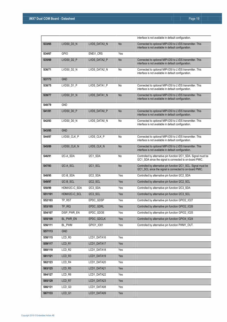
iMX7 Dual COM Board - Datasheet Page 19
Copyright 2016 © Embedded Artists AB
interface is not available in default configuration.
S33/65 LVDS0_D3_N LVDS_DATA3_N No Connected to optional MIPI-DSI to LVDS transmitter. This interface is not available in default configuration.
S34/67 GPIO ENEt1_CRS Yes
S35/69 LVDS0_D2_P LVDS_DATA2_P No Connected to optional MIPI-DSI to LVDS transmitter. This interface is not available in default configuration.
S36/71 LVDS0_D2_N LVDS_DATA2_N No Connected to optional MIPI-DSI to LVDS transmitter. This interface is not available in default configuration.
S37/73 GND
S38/75 LVDS0_D1_P LVDS_DATA1_P No Connected to optional MIPI-DSI to LVDS transmitter. This interface is not available in default configuration.
S39/77 LVDS0_D1_N LVDS_DATA1_N No Connected to optional MIPI-DSI to LVDS transmitter. This interface is not available in default configuration.
S40/79 GND
S41/81 LVDS0_D0_P LVDS_DATA0_P No Connected to optional MIPI-DSI to LVDS transmitter. This interface is not available in default configuration.
S42/83 LVDS0_D0_N LVDS_DATA0_N No Connected to optional MIPI-DSI to LVDS transmitter. This interface is not available in default configuration.
S43/85 GND
S44/87 LVDS0_CLK_P LVDS_CLK_P No Connected to optional MIPI-DSI to LVDS transmitter. This interface is not available in default configuration.
S45/89 LVDS0_CLK_N LVDS_CLK_N No Connected to optional MIPI-DSI to LVDS transmitter. This interface is not available in default configuration.
S46/91 I2C-A_SDA I2C1_SDA No Controlled by alternative pin function I2C1_SDA. Signal must be I2C1_SDA since the signal is connected to on-board PMIC.
S47/93 I2C-A_SCL I2C1_SCL No Controlled by alternative pin function I2C1_SCL. Signal must be I2C1_SCL since the signal is connected to on-board PMIC.
S48/95 I2C-B_SDA I2C2_SDA Yes Controlled by alternative pin function I2C2_SDA
S49/97 I2C-B_SCL I2C2_SCL Yes Controlled by alternative pin function I2C2_SCL
S50/99 HDMI/I2C-C_SDA I2C3_SDA Yes Controlled by alternative pin function I2C3_SDA
S51/101 HDMI/I2C-C_SCL I2C3_SCL Yes Controlled by alternative pin function I2C3_SCL
S52/103 TP_RST EPDC_GDSP Yes Controlled by alternative pin function GPIO2_IO27
S53/105 TP_IRQ EPDC_GDRL Yes Controlled by alternative pin function GPIO2_IO26
S54/107 DISP_PWR_EN EPDC_GDOE Yes Controlled by alternative pin function GPIO2_IO25
S55/109 BL_PWR_EN EPDC_GDCLK Yes Controlled by alternative pin function GPIO4_IO24
S56/111 BL_PWM GPIO1_IO01 Yes Controlled by alternative pin function PWM1_OUT.
S57/113 GND
S58/115 LCD_R0 LCD1_DATA16 Yes
S59/117 LCD_R1 LCD1_DATA17 Yes
S60/119 LCD_R2 LCD1_DATA18 Yes
S61/121 LCD_R3 LCD1_DATA19 Yes
S62/123 LCD_R4 LCD1_DATA20 Yes
S63/125 LCD_R5 LCD1_DATA21 Yes
S64/127 LCD_R6 LCD1_DATA22 Yes
S65/129 LCD_R7 LCD1_DATA23 Yes
S66/131 LCD_G0 LCD1_DATA08 Yes
S67/133 LCD_G1 LCD1_DATA09 Yes

iMX7 Dual COM Board - Datasheet Page 20
Copyright 2016 © Embedded Artists AB
S68/135 LCD_G2 LCD1_DATA10 Yes
S69/137 LCD_G3 LCD1_DATA11 Yes
S70/139 LCD_G4 LCD1_DATA12 Yes
S71/141 LCD_G5 LCD1_DATA13 Yes
S72/143 LCD_G6 LCD1_DATA14 Yes
S73/145 LCD_G7 LCD1_DATA15 Yes
S74/147 GND
S75/149 LCD_B0 LCD1_DATA00 Yes
151 Non existing pin
153 Non existing pin
155 Non existing pin
S76/157 LCD_B1 LCD1_DATA01 Yes
S77/159 LCD_B2 LCD1_DATA02 Yes
S78/161 LCD_B3 LCD1_DATA03 Yes
S79/163 LCD_B4 LCD1_DATA04 Yes
S80/165 LCD_B5 LCD1_DATA05 Yes
S81/167 LCD_B6 LCD1_DATA06 Yes
S82/169 LCD_B7 LCD1_DATA07 Yes
S83/171 LCD_CLK LCD1_CLK Yes
S84/173 GPIO7 LCD1_RESET Yes Controlled by alternative pin function GPIO3_IO04.
S85/175 LCD_HSYNC LCD1_HSYNC Yes
S86/177 LCD_VSYNC LCD1_VSYNC Yes
S87/179 LCD_ENABLE LCD1_ENABLE Yes
S88/181 GND
S89/183 AIN_VREF VDDA_ADCx_1P8, i.MX 7 SoC balls AC3 and AB3
No Supply voltage (1.8V) for i.MX7 SoC on-chip ADC
S90/185 AIN7 ADC2_IN3 No Note that voltage range is 0-1.8V.
S91/187 AIN6 ADC2_IN2 No Note that voltage range is 0-1.8V.
S92/189 AIN5 ADC2_IN1 No Note that voltage range is 0-1.8V.
S93/191 AIN4 ADC2_IN0 No Note that voltage range is 0-1.8V.
S94/193 AIN3 ADC1_IN3 No Note that voltage range is 0-1.8V.
S95/195 AIN2 ADC1_IN2 No Note that voltage range is 0-1.8V.
S96/197 AIN1 ADC1_IN1 No Note that voltage range is 0-1.8V.
Optional, non-standard pin allocation with signal MIPI_DSI_D1_P possible.
S97/199 AIN0 ADC1_IN0 No Note that voltage range is 0-1.8V.
Optional, non-standard pin allocation with signal MIPI_DSI_D1_N possible.
S98/201 GND
S99/203 COM board specific MIPI_DSI_D0_P No
S100/205 COM board specific MIPI_DSI_D0_N No
S101/207 GND
S102/209 COM board specific MIPI_DSI_CLK_P No

iMX7 Dual COM Board - Datasheet Page 21
Copyright 2016 © Embedded Artists AB
S103/211 COM board specific MIPI_DSI_CLK_N No
S104/213 GND
S105/215 COM board specific SNVS_TAMPER8 No
S106/217 COM board specific SNVS_TAMPER7 No
S107/219 COM board specific SNVS_TAMPER6 No
S108/221 COM board specific SNVS_TAMPER5 No
S109/223 COM board specific SNVS_TAMPER4 No
S110/225 COM board specific SNVS_TAMPER3 No
S111/227 COM board specific SD1_WP Yes
S112/229 COM board specific I2C4_SDA Yes
S113/231 COM board specific I2C4_SCL Yes
S114/233 CSI_HSYNC
S115/235 CSI_VSYNC GPIO1_IO11/ ETH_PHY_MDC
No Signal allocated for ETH_PHY_MDC and used by on-board Ethernet-PHY. Signal can be used for external Ethernet-PHY for second Ethernet interface.
S116/237 CSI_MCLK GPIO1_IO10/ ETH_PHY_MDIO
No Signal allocated for ETH_PHY_MDIO and used by on-board Ethernet-PHY. Signal can be used for external Ethernet-PHY for second Ethernet interface.
S117/239 CSI_PCLK Do not connect to this pin. Internally it is connected to the PMIC interrupt.
S118/241 GND
S119/243 CSI_D0 SD1_VSELECT No Input to control voltage level of SD interface. Leave open for 3.3V interface voltage. Pull signal high for 1.8V interface voltage.
Connect to GPIO1_IO08 to control SD interface voltage via GPIO.
S120/245 CSI_D1 SNVS_TAMPER9 No
S121/247 CSI_D2 EPDC_SDSHR Yes
S122/249 CSI_D3 SD2_CD Yes
S123/251 CSI_D4 SD2_RESET Yes
S124/253 CSI_D5 SD2_WP Yes
S125/255 CSI_D6
S126/257 CSI_D7
S127/259 GND
S128/261 CSI_D3_M MIPI-CSI interface has only 2 lanes.
S129/263 CSI_D3_P MIPI-CSI interface has only 2 lanes.
S130/265 GND
S131/267 CSI_D2_M MIPI-CSI interface has only 2 lanes.
S132/269 CSI_D2_P MIPI-CSI interface has only 2 lanes.
S133/271 GND
S134/273 CSI_D1_M MIPI_CSI_D1_N No
S135/275 CSI_D1_P MIPI_CSI_D1_P No
S136/277 GND
S137/279 CSI_D0_M MIPI_CSI_D0_N No
S138/281 CSI_D0_P MIPI_CSI_D0_P No
S139/283 GND

iMX7 Dual COM Board - Datasheet Page 22
Copyright 2016 © Embedded Artists AB
S140/285 CSI_CLK_M MIPI_CSI_CLK_N No
S141/287 CSI_CLK_P MIPI_CSI_CLK_P No
S142/289 GND
S143/291 SATA_TX_P
S144/293 SATA_TX_N
S145/295 GND
S146/297 SATA_RX_N PCIE_REFCLKIN_N No If PCIe is used, connect to a 100MHz PCIe compatible reference clock with HCSL-signal output, negative signal
S147/299 SATA_RX_P PCIE_REFCLKIN_P No If PCIe is used, connect to a 100MHz PCIe compatible reference clock with HCSL-signal output, positive signal
S148/301 GND
S149/303 GND
S150/305 PCIE_CLK_P PCIE_REFCLKOUT_P No
S151/307 PCIE_CLK_N PCIE_REFCLKOUT_N No
S152/309 GND
S153/311 PCIE_TX_P PCIE_TX_P No
S154/313 PCIE_TX_N PCIE_TX_N No
S155/315 GND
S156/317 PCIE_RX_P PCIE_RX_P No
S157/319 PCIE_RX_N PCIE_RX_N No
S158/321 GND
iMX7 Dual COM Board - Datasheet Page 23
Copyright 2016 © Embedded Artists AB
4 Pin Mapping
4.1 Functional Multiplexing on I/O Pins
There are a lot of different peripherals inside the i.MX 7Dual SoC. Many of these peripherals are connected to the IOMUX block, that allows the I/O pins to be configured to carry one of many (up to nine different) alternative functions. This leave great flexibility to select a function multiplexing scheme for the pins that satisfy the interface need for a particular application.
Some interfaces with specific voltage levels/drivers/transceivers have dedicated pins, like ADC, PCIe, MIPI-DSI, MIPI-CSI and USB. i.MX 7Dual pins carrying these signals do not have any functional multiplexing possibilities. These interfaces are fixed.
To keep compatibility between EACOM boards the EACOM specified pinning should be followed, but in general there are no restrictions to select alternative pin multiplexing schemes on the iMX7 Dual COM Board. Note that all EACOM-defined pins are not connected on some EACOM boards, typically because an interface is not supported or there are not enough free pins in the SoC. Further, some EACOM board pins are type specific, meaning that these pins might not be compatible with other EACOM boards. Using type specific pins may result in lost compatibility between EACOM boards, but not always. Always check details between EACOM boards of interest.
If switching between EACOM board is not needed, then pin multiplexing can be done without considering the EACOM pin allocation. A custom carrier board design is needed in this case.
Functional multiplexing is normally controlled via the Linux BSP. It can also be done directly via
register IOMUXC_LPSR_SW_MUX_CTL_PAD_xxx /
IOMUXC_SW_MUX_CTL_PAD_xxx where xxx is the name of the i.MX 7Dual pin. For more
information about the register settings, see the i.MX 7Dual Application Processor Reference Manual from NXP.
Note that input functions that are available on multiple pins will require control of an input multiplexer.
This is controlled via register IOMUXC_xxx_SELECT_INPUT where xxx is the name of the
input function. Again, for more information about the register settings, see the i.MX 7Dual Application Processor Reference Manual from NXP.
4.1.1 Alternative I/O Function List
There is an accompanying Excel document that lists all alternative functions for each available I/O pin. The reset state is shown as well as the EACOM function allocation. The reset state is typically GPIO, ALT5 function, except for the GPIO1_IO01-15 signals that are ALT0 functions, but that is the GPIO function.
4.2 I/O Pin Control
Each pin also has an additional control register for configuring input hysteresis, pull up/down resistors, push-pull/open-drain driving, drive strength and more. Also in this case, configuration is normally done via the Linux BSP but it is possible to directly access the control registers, which are called
IOMUXC_SW_PAD_CTL_PAD_xxx where xxx is the name of the i.MX 7Dual pin. For more
information about the register settings, see the i.MX 7Dual Application Processor Reference Manual from NXP.
As a general recommendation, select slow slew rate and lowest drive strength (that still result in acceptable signal edges for the system) in order to reduce problems with EMC.
Note that many pins (but not all) are configured as GPIO inputs, with a 100Kohm pull-down resistor, after reset. When the bootloader (typically u-boot) executes it is possible to reconfigure the pins.
iMX7 Dual COM Board - Datasheet Page 24
Copyright 2016 © Embedded Artists AB
5 Interface Description This chapter lists details about all different interfaces. The i.MX 7Dual datasheet and user manual should always be consulted for details about different functions and interfaces. Many interfaces are multiplexed on different pins and not available simultaneously.
Note that this chapter do not list all peripheral functions available on the i.MX7 Dual SoC. Only the ones related to the EACOM specification. For all available interfaces, consult Chapter 8 - Chip IO and pinmux, Section 8.1 External Signals and Pin Multiplexing in NXP's i.MX 7Dual Applications Processor Reference Manual (document id: IMX7DRM).
Example of peripheral blocks not listed in this chapter are listed below (see document IMX7DRM for details). Some of the blocks have multiple instances.
CCM - Clock Controller Module
Besides internal clocks, this peripheral can generate external clocks.
EIM - External Interface Module
This peripheral provides asynchronous access to devices with SRAM-like interface and
synchronous access to devices with NOR-Flash-like or PSRAM-like interface.
EPDC - Electrophoretic Display Controller
This peripheral is a controller for E-INKTM displays.
FTM - Flex Timer
This peripheral is a flexible timer that supports input capture and can generate PWM signals.
GPT - General Purpose Timer
This peripheral is a 32-bit general purpose timer with capture and trigger functions.
KPP - Keypad Port
This peripheral provides a keypad matrix interface.
SDMA - Smart Direct Memory Access Controller
This peripheral provides fast data transfers between peripheral I/O devices and
internal/external memories
SIM - Subscriber Identification Module
This peripheral provides an interface to SIM cards and is compatible with ISO/IEC 7816-3.
WDOG - Watchdog Timer
This peripheral implements a watchdog timer.
There is an accompanying Excel document that lists all alternative functions for each available I/O pin.

iMX7 Dual COM Board - Datasheet Page 25
Copyright 2016 © Embedded Artists AB
5.1 Camera Interfaces
This section lists signals related to CMOS Sensor Interface (CSI) functions.
There are two camera interfaces, one parallel and one serial (MIPI-CSI2) input interface. One at a time is multiplexed to the CSI unit. The picture below illustrates the multiplexing and where the EACOM allocated interface are connected. Note that the 8-bit parallel camera interface of the EACOM Board specification has not been allocated.
Figure 4 – Camera Port Multiplexing Scheme
5.1.1 Parallel Camera Interface
This section lists signals for the parallel camera interface.
The EACOM Board specification defines an 8-bit parallel camera interface. This interface has not been allocated.
The table below lists the pin assignment that has been done on the pins that are associated with the 8-bit parallel camera input interface of the EACOM Board specification.
EACOM Board Pin
EACOM Board Name
i.MX 7 Ball Name I/O Description Remarks
S116/237 CSI_MCLK GPIO1_IO10-ETH_PHY_MDIO
I/O Non-standard pin allocation.
Signal allocated for ETH_PHY_MDIO and used by on-board Ethernet-PHY. Signal can be used for external Ethernet-PHY for second Ethernet interface.
S117/239 CSI_PIXCLK Non-standard pin allocation.
Do not connect to this pin. Internally it is connected to the PMIC interrupt.
S114/233 CSI_HSYNC Not connected.
S115/235 CSI_VSYNC GPIO1_IO11/ ETH_PHY_MDC
O Non-standard pin allocation.
Signal allocated for ETH_PHY_MDC and used by on-board Ethernet-PHY. Signal can be used for external Ethernet-PHY for second Ethernet interface.
S119/243 CSI_D0 SD1_VSELECT I Non-standard pin allocation.
Input to control voltage level of SD interface. Leave open for 3.3V interface voltage. Pull signal high for 1.8V interface voltage.
Connect to GPIO1_IO08 to control SD interface
Parallel camera interface is NOT EACOM allocated
EACOM allocated serial camera interface

iMX7 Dual COM Board - Datasheet Page 26
Copyright 2016 © Embedded Artists AB
voltage via GPIO.
S120/245 CSI_D1 SNVS_TAMPER9 I Non-standard pin allocation.
S121/247 CSI_D2 EPDC_SDSHR I/O Non-standard pin allocation.
S122/249 CSI_D3 SD2_CD I/O Non-standard pin allocation.
S123/251 CSI_D4 SD2_RESET I/O Non-standard pin allocation.
S124/253 CSI_D5 SD2_WP I/O Non-standard pin allocation.
S125/255 CSI_D6 Not connected.
S126/257 CSI_D7 Not connected.
The table below lists the alternative pin locations for the parallel camera interface.
EACOM Board Pin
EACOM Board Name i.MX 7 Ball Name I/O Description Remarks
S59/117 LCD_R1 LCD1_DATA17 I Data Sensor Signal Alternative location for CSI_DATA00
S58/115 LCD_R0 LCD1_DATA16 I Data Sensor Signal Alternative location for CSI_DATA01
P126/260 SPI-A_CLK ECSPI1_SCLK I Data Sensor Signal Alternative location for CSI_DATA02
S73/145 LCD_G7 LCD1_DATA15 I Data Sensor Signal Alternative location for CSI_DATA02
P124/256 SPI-A_MOSI ECSPI1_MOSI I Data Sensor Signal Alternative location for CSI_DATA03
S72/143 LCD_G6 LCD1_DATA14 I Data Sensor Signal Alternative location for CSI_DATA03
P125/258 SPI-A_MISO ECSPI1_MISO I Data Sensor Signal Alternative location for CSI_DATA04
S71/141 LCD_G5 LCD1_DATA13 I Data Sensor Signal Alternative location for CSI_DATA04
P123/254 SPI-A_SSEL ECSPI1_SS0 I Data Sensor Signal Alternative location for CSI_DATA05
S70/139 LCD_G4 LCD1_DATA12 I Data Sensor Signal Alternative location for CSI_DATA05
P122/252 SPI-B_CLK ECSPI2_SCLK I Data Sensor Signal Alternative location for CSI_DATA06
S69/137 LCD_G3 LCD1_DATA11 I Data Sensor Signal Alternative location for CSI_DATA06
P120/248 SPI-B_MOSI ECSPI2_MOSI I Data Sensor Signal Alternative location for CSI_DATA07
S68/135 LCD_G2 LCD1_DATA10 I Data Sensor Signal Alternative location for CSI_DATA07
P121/250 SPI-B_MISO ECSPI2_MISO I Data Sensor Signal Alternative location for CSI_DATA08
S67/133 LCD_G1 LCD1_DATA09 I Data Sensor Signal Alternative location for CSI_DATA08
P119/246 SPI-B_SSEL ECSPI2_SS0 I Data Sensor Signal Alternative location for CSI_DATA09
S66/131 LCD_G0 LCD1_DATA08 I Data Sensor Signal Alternative location for CSI_DATA09
S65/129 LCD_R7 LCD1_DATA23 I Data Sensor Signal Alternative location for CSI_DATA10
S64/127 LCD_R6 LCD1_DATA22 I Data Sensor Signal Alternative location for CSI_DATA11
S63/125 LCD_R5 LCD1_DATA21 I Data Sensor Signal Alternative location for CSI_DATA12
S62/123 LCD_R4 LCD1_DATA20 I Data Sensor Signal Alternative location for CSI_DATA13
S61/121 LCD_R3 LCD1_DATA19 I Data Sensor Signal Alternative location for CSI_DATA14
S60/119 LCD_R2 LCD1_DATA18 I Data Sensor Signal Alternative location for CSI_DATA15
S83/171 LCD_CLK LCD1_CLK I Data Sensor Signal Alternative location for CSI_DATA16
S87/179 LCD_ENABLE LCD1_ENABLE I Data Sensor Signal Alternative location for CSI_DATA17
S85/175 LCD_HSYNC LCD1_HSYNC I Data Sensor Signal Alternative location for CSI_DATA18
S86/177 LCD_VSYNC LCD1_VSYNC I Data Sensor Signal Alternative location for CSI_DATA19
S75/149 LCD_B0 LCD1_DATA00 I Data Sensor Signal Alternative location for CSI_DATA20
S76/157 LCD_B1 LCD1_DATA01 I Data Sensor Signal Alternative location for CSI_DATA21
iMX7 Dual COM Board - Datasheet Page 27
Copyright 2016 © Embedded Artists AB
S77/159 LCD_B2 LCD1_DATA02 I Data Sensor Signal Alternative location for CSI_DATA22
S78/161 LCD_B3 LCD1_DATA03 I Data Sensor Signal Alternative location for CSI_DATA23
S84/173 GPIO7 LCD1_RESET I CSI Field Signal Alternative location for CSI_FIELD
S50/99 HDMI/I2C-C_SDA I2C3_SDA I Horizontal Sync Alternative location for CSI_HSYNC
Note that there is a 2.2Kohm pull-up resistor on this signal.
S80/165 LCD_B5 LCD1_DATA05 I Horizontal Sync Alternative location for CSI_HSYNC
S112/229 COM specific I2C4_SDA O Master Clock Alternative location for CSI_MCLK
S82/169 LCD_B7 LCD1_DATA07 O Master Clock Alternative location for CSI_MCLK
S113/231 COM specific I2C4_SCL I Pixel Clock Alternative location for CSI_PIXCLK
S81/167 LCD_B6 LCD1_DATA06 I Pixel Clock Alternative location for CSI_PIXCLK
S51/101 HDMI/I2C-C_SCL I2C3_SCL I Vertical Sync Alternative location for CSI_VSYNC
Note that there is a 2.2Kohm pull-up resistor on this signal.
S79/163 LCD_B4 LCD1_DATA04 I Vertical Sync Alternative location for CSI_VSYNC
The CSI can support connection with the sensor as follows.
To connect with a 8-bit sensor, the sensor data interface should connect to CSI_DATA[9:2].
To connect with a 10-bit sensor, the sensor data interface should connect to CSI_DATA[9:0].
To connect with a 16-bit sensor, the sensor data interface should connect to CSI_DATA[15:0].
To connect with two 8-bit sensors, the sensor data interfaces should connect to CSI_DATA[7:0] and CSI_DATA[15:8], respectively.
The CSI input data format mapping is shown in the table below.
Internal CSI Signal Name
TVdecoder YCbCr 1 cycle
RGB888 1 cycle
RGB888/ YUV4444 3 cycles
RGB666 1 cycle
RGB565 1 cycle
YCbCr422 1 cycle
YCbCr422 2 cycles
Generic 10 bit
CCIR656
CSI_DATA23 Y7 R7 R5
CSI_DATA22 Y6 R6 R4
CSI_DATA21 Y5 R5 R3
CSI_DATA20 Y4 R4 R2
CSI_DATA19 Y3 R3 R1
CSI_DATA18 Y2 R2 R0
CSI_DATA17 Y1 R1 Y5
CSI_DATA16 Y0 R0 Y4
CSI_DATA15 Cb7 G7 G5 R4 Y7
CSI_DATA14 Cb6 G6 G4 R3 Y6
CSI_DATA13 Cb5 G5 G3 R2 Y5
CSI_DATA12 Cb4 G4 G2 R1 Y4
CSI_DATA11 Cb3 G3 G1 R0 Y3
CSI_DATA10 Cb2 G2 G0 G5 Y2
CSI_DATA09 Cb1 G1 R7/G7/B7 G5 G4 Y1 Y7/C7 Ge9 C7/Y7
CSI_DATA08 Cb0 G0 R6/G6/B6 G4 G3 Y0 Y6/C6 Ge8 C6/Y6
CSI_DATA07 Cr7 B7 R5/G5/B5 B5 G2 C7 Y5/C5 Ge7 C5/Y5

iMX7 Dual COM Board - Datasheet Page 28
Copyright 2016 © Embedded Artists AB
CSI_DATA06 Cr6 B6 R4/G4/B4 B4 G1 C6 Y4/C4 Ge6 C4/Y4
CSI_DATA05 Cr5 B5 R3/G3/B3 B3 G0 C5 Y3/C3 Ge5 C3/Y3
CSI_DATA04 Cr4 B4 R2/G2/B2 B2 B4 C4 Y2/C2 Ge4 C2/Y2
CSI_DATA03 Cr3 B3 R1/G1/B1 B1 B3 C3 Y1/C1 Ge3 C1/Y1
CSI_DATA02 Cr2 B2 R0/G0/B0 B0 B2 C2 Y0/C0 Ge2 C0/Y0
CSI_DATA01 Cr1 B1 B5 B1 C1 Ge1
CSI_DATA00 Cr0 B0 B4 B0 C0 Ge0
5.1.2 Serial Camera Interface
This section lists signals for the serial camera interface, also called MIPI-CSI2.
The EACOM Board specification defines an serial camera interface, MIPI-CSI2 with up to 2 lanes. The table below lists the pin assignment according to EACOM Board specification.
EACOM Board Pin
EACOM Board Name
i.MX 7 Ball Name I/O Description Remarks
S141/287 CSI_CLK_P MIPI_CSI_CLK0P I Positive D-Phy differential clock line Receiver input
S140/285 CSI_CLK_N MIPI_CSI_CLK0N I Negative D-Phy differential clock line Receiver input
S138/281 CSI_D0_P MIPI_CSI_D0P I Positive D-Phy differential data line Receiver input , Lane 0
S137/279 CSI_D0_N MIPI_CSI_D0N I Negative D-Phy differential data line Receiver input , Lane 0
S135/275 CSI_D1_P MIPI_CSI_D1P I Positive D-Phy differential data line Receiver input , Lane 1
S134/273 CSI_D1_N MIPI_CSI_D1N I Negative D-Phy differential data line Receiver input , Lane 1
S132/269 CSI_D2_P Not connected
S131/267 CSI_D2_N Not connected
S129/263 CSI_D3_P Not connected
S128/261 CSI_D3_N Not connected

iMX7 Dual COM Board - Datasheet Page 29
Copyright 2016 © Embedded Artists AB
5.2 Display Interfaces
This section lists signals related to display output interfaces; parallel RGB (Enhanced LCD Interface - eLCDIF) and MIPI-DSI transmitter.
The i.MX 7Dual SoC has a display and graphics subsystem with dedicated components:
PXP pixel pipeline: pixel/image processing engine for LCD display
LCD interface (LCDIF), which is 24-bit parallel RGB LCD interface
CSI interface with up to 24-bit parallel interface for image sensor
EPDC interface for E-INKTM displays. This interface will not be presented further in this document. For more details, see NXP document IMX7DRM.
The picture below shows the high-level structure of the display and graphics subsystem. It picture comes from chapter 13 - Multimedia in the IMX7DRM.
Figure 5 – Structure of Display and Graphics Subsystem
The i.MX 7Dual COM board has allocated pins (according to the EACOM Board specification) for one serial camera input, a parallel RGB LCD output and a serial display output. The EACOM pins for LVDS and HDMI output interfaces are not allocated since the i.MX 7Dual SoC does not support these interfaces. The serial camera interface is presented in section 5.1 .
iMX7 Dual COM Board - Datasheet Page 30
Copyright 2016 © Embedded Artists AB
The EACOM Board specification has allocated some additional support signals that are typically needed to implement a display interface. The table below list these signals. These are common for all display interfaces.
EACOM Board Pin
EACOM Board Name
i.MX 7 Ball Name I/O Description Remarks
S56/111 BL_PWM GPIO1_IO01 O PWM signal to control backlight contrast.
Signal is connected to PWM1_OUT
S55/109 BL_PWR_EN EPDC_GDCLK O Power control for backlight. Active high
Signal is connected to GPIO2_IO24
S54/107 DISP_PWR_EN EPDC_GDOE O Power control for LCD power supply. Active high
Signal is connected to GPIO2_IO25
S53/105 TP_IRQ EPDC_GDRL I Interrupt from touch controller Signal is connected to GPIO2_IO26
S52/103 TP_RST EPDC_GDSP O Reset signal to touch controller. Active low
Signal is connected to GPIO2_IO27
S47/93 I2C-A_SCL I2C1_SCL I/O Clock signal of I2C channel A It is recommended to connect the RGB LCD touch controller (if I2C interface) to this channel.
S46/91 I2C-A_SDA I2C1_SDA I/O Data signal of I2C channel A It is recommended to connect the RGB LCD touch controller (if I2C interface) to this channel.
S49/97 I2C-B_SCL I2C2_SCL I/O Clock signal of I2C channel B A touch controller can be connected to this I2C channels also, but will require adjustment in Linux BSP.
S48/95 I2C-B_SDA I2C2_SDA I/O Data signal of I2C channel B A touch controller can be connected to this I2C channels also, but will require adjustment in Linux BSP.
S51/101 I2C-C_SCL I2C3_SCL I/O Clock signal of I2C channel C A touch controller can be connected to this I2C channels also, but will require adjustment in Linux BSP.
S50/99 I2C-C_SDA I2C3_SDA I/O Data signal of I2C channel C A touch controller can be connected to this I2C channels also, but will require adjustment in Linux BSP.
5.2.1 Parallel RGB LCD Interface
This section lists signals for the parallel RGB LCD interface.
The parallel RGB LCD interface with 24-bit color depth. It can for example drive 1080p (1920x1080 pixel) at 60 fps.
The parallel RGB LCD interface is ideal for smaller, lower resolution displays. Note that due to EMI MIPI-DSI might be better choices of interface for high resolution displays.
Note that both the parallel RGB and MIPI-DSI interfaces will carry the same display output data. Only one display output data stream is possible at a time.
The EACOM Board specification defines a 24-bit parallel LCD interface. The table below lists the pin assignment according to EACOM Board specification. For best portability it is recommended to always have the LCD interface running in 24-bit mode. If less bits are needed in a specific LCD implementation the LSB bits of each color is just ignored, see the three rightmost columns.

iMX7 Dual COM Board - Datasheet Page 31
Copyright 2016 © Embedded Artists AB
EACOM Board Pin
EACOM Board Name
i.MX 7 Ball Name
I/O Color Config. for 16-bit 565RGB
Color Config. for 18-bit 666RGB
Color Config. for 16-bit 565RGB if interface set to 24-bit
Color Config. for 18-bit 666RGB if interface set to 24-bit
Color Config. for 24-bit 888RGB
S75/149 LCD_DATA00 LCD1_DATA00 O B0 B0 B0
S76/157 LCD_DATA01 LCD1_DATA01 O B1 B1 B1
S77/159 LCD_DATA02 LCD1_DATA02 O B2 B2 B2 B2
S78/161 LCD_DATA03 LCD1_DATA03 O B3 B3 B3 B3 B3
S79/163 LCD_DATA04 LCD1_DATA04 O B4 B4 B4 B4 B4
S80/165 LCD_DATA05 LCD1_DATA05 O G0 B5 B5 B5 B5
S81/167 LCD_DATA06 LCD1_DATA06 O G1 G0 B6 B6 B6
S82/169 LCD_DATA07 LCD1_DATA07 O G2 G1 B7 B7 B7
S66/131 LCD_DATA08 LCD1_DATA08 O G3 G2 G0
S67/133 LCD_DATA09 LCD1_DATA09 O G4 G3 G1
S68/135 LCD_DATA10 LCD1_DATA10 O G7 G4 G2 G2 G2
S69/137 LCD_DATA11 LCD1_DATA11 O R0 G5 G3 G3 G3
S70/139 LCD_DATA12 LCD1_DATA12 O R1 R0 G4 G4 G4
S71/141 LCD_DATA13 LCD1_DATA13 O R2 R1 G5 G5 G5
S72/143 LCD_DATA14 LCD1_DATA14 O R3 R2 G6 G6 G6
S73/145 LCD_DATA15 LCD1_DATA15 O R4 R3 G7 G7 G7
S58/115 LCD_DATA16 LCD1_DATA16 O R4 R0
S59/117 LCD_DATA17 LCD1_DATA17 O R5 R1
S60/119 LCD_DATA18 LCD1_DATA18 O R2 R2
S61/121 LCD_DATA19 LCD1_DATA19 O R3 R3 R3
S62/123 LCD_DATA20 LCD1_DATA20 O R4 R4 R4
S63/125 LCD_DATA21 LCD1_DATA21 O R5 R5 R5
S64/127 LCD_DATA22 LCD1_DATA22 O R6 R6 R6
S65/129 LCD_DATA23 LCD1_DATA23 O R7 R7 R7
S85/175 LCD_HSYNC LCD1_HSYNC O Horizontal (line) synchronization
S86/177 LCD_VSYNC LCD1_VSYNC O Vertical (frame) synchronization
S87/179 LCD_ENABLE LCD1_ENABLE O Data enable
S83/171 LCD_CLK LCD1_CLK O Pixel (dot) clock
Note that the eLCDIF peripheral in the i.MX 7Dual SoC also supports MPU-like display interfaces. See chapter 13, section 13.2 in IMX7DRM for more details.
5.2.2 MIPI-DSI Interface
This section lists signals for the MIPI-DSI interface. The interface supports display resolutions up to 1400x1050 pixels (SXGA+) with 24-bit resolution at 60 fps.
Note that both the parallel RGB and MIPI-DSI interfaces will carry the same display output data. Only one display output data stream is possible at a time.

iMX7 Dual COM Board - Datasheet Page 32
Copyright 2016 © Embedded Artists AB
The EACOM Board specification has not allocated pins for this interface, since it is mostly used in very high volume applications (where COM boards are not so commonly used). The MIPI-DSI interface supports two data lanes and together with the clock signal, six pins as been used.
EACOM Board Pin
EACOM Board Name
i.MX 7 Ball Name I/O Description Remarks
S102/209 COM specific MIPI_DSI_CLK0M O Differential clock pair, negative signal
S103/211 COM specific MIPI_DSI_CLK0P O Differential clock pair, positive signal
S99/203 COM specific MIPI_DSI_D0M I/O Differential data pair #0, negative signal
S100/205 COM specific MIPI_DSI_D0P I/O Differential data pair #0, positive signal
S96/197 AIN1 Optionally MIPI_DSI_D1M
O Differential data pair #1, negative signal Note that this signal is not available by default.
S97/199 AIN0 Optionally MIPI_DSI_D1P
O Differential data pair #1, positive signal Note that this signal is not available by default.
5.3 Digital Audio Interfaces: Synchronous Audio Interfaces (SAI)
This section lists signals related to the Digital Audio Interfaces.
The i.MX 7 SoC contains an audio subsystem. It consists of three Synchronous Audio Interfaces (SAI1-SAI3) and a Medium Quality Speaker Interface (MQS). In addition, the IOMUX block allows the signals to get in and out of the SoC via configured pins.
Each SAI block is a full-duplex serial port with frame synchronization that allows communication with external devices using a variety of serial protocols (like I2S, AC-97, TDM and codec/DSP interfaces), up to 32-bits per word and different clock/frame options.
The three SAI interfaces and MQS block are directly connected to the IOMUX.
Figure 6 – Audio Subsystem Block Diagram
The table below lists pins that have been allocated according to the EACOM Board specification. The SAI1 port is used with synchronous transmit and receive sections (meaning that transmit and receive share the clock and frame synch signals).
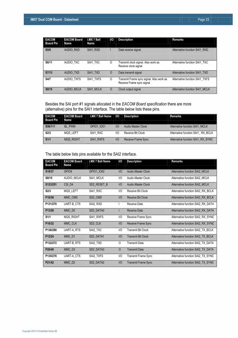
iMX7 Dual COM Board - Datasheet Page 33
Copyright 2016 © Embedded Artists AB
EACOM Board Pin
EACOM Board Name
i.MX 7 Ball Name
I/O Description Remarks
S5/9 AUDIO_RXD SAI1_RXD I Data receive signal Alternative function SAI1_RXD
S6/11 AUDIO_TXC SAI1_TXC O Transmit clock signal. Also work as Receive clock signal
Alternative function SAI1_TXC
S7/13 AUDIO_TXD SAI1_TXD O Data transmit signal Alternative function SAI1_TXD
S4/7 AUDIO_TXFS SAI1_TXFS O Transmit Frame sync signal. Also work as Receive Frame sync signal
Alternative function SAI1_TXFS
S8/15 AUDIO_MCLK SAI1_MCLK O Clock output signal Alternative function SAI1_MCLK
Besides the SAI port #1 signals allocated in the EACOM Board specification there are more (alternative) pins for the SAI1 interface. The table below lists these pins.
EACOM Board Pin
EACOM Board Name
i.MX 7 Ball Name I/O Description Remarks
S56/111 BL_PWM GPIO1_IO01 I/O Audio Master Clock Alternative function SAI1_MCLK
S2/3 MQS_LEFT SAI1_RXC I/O Receive Bit Clock Alternative function SAI1_ RX_BCLK
S1/1 MQS_RIGHT SAI1_RXFS I/O Receive Frame Sync Alternative function SAI1_RX_SYNC
The table below lists pins available for the SAI2 interface.
EACOM Board Pin
EACOM Board Name
i.MX 7 Ball Name I/O Description Remarks
S19/37 GPIO9 GPIO1_IO02 I/O Audio Master Clock Alternative function SAI2_MCLK
S8/15 AUDIO_MCLK SAI1_MCLK I/O Audio Master Clock Alternative function SAI2_MCLK
S123/251 CSI_D4 SD2_RESET_B I/O Audio Master Clock Alternative function SAI2_MCLK
S2/3 MQS_LEFT SAI1_RXC I/O Receive Bit Clock Alternative function SAI2_RX_BCLK
P18/36 MMC_CMD SD2_CMD I/O Receive Bit Clock Alternative function SAI2_RX_BCLK
P131/270 UART-B_CTS SAI2_RXD I Receive Data Alternative function SAI2_RX_DATA
P13/26 MMC_D0 SD2_DATA0 I Receive Data Alternative function SAI2_RX_DATA
S1/1 MQS_RIGHT SAI1_RXFS I/O Receive Frame Sync Alternative function SAI2_RX_SYNC
P16/32 MMC_CLK SD2_CLK I/O Receive Frame Sync Alternative function SAI2_RX_SYNC
P136/280 UART-A_RTS SAI2_TXC I/O Transmit Bit Clock Alternative function SAI2_TX_BCLK
P12/24 MMC_D1 SD2_DATA1 I/O Transmit Bit Clock Alternative function SAI2_TX_BCLK
P132/272 UART-B_RTS SAI2_TXD O Transmit Data Alternative function SAI2_TX_DATA
P20/40 MMC_D3 SD2_DATA3 O Transmit Data Alternative function SAI2_TX_DATA
P135/278 UART-A_CTS SAI2_TXFS I/O Transmit Frame Sync Alternative function SAI2_TX_SYNC
P21/42 MMC_D2 SD2_DATA2 I/O Transmit Frame Sync Alternative function SAI2_TX_SYNC

iMX7 Dual COM Board - Datasheet Page 34
Copyright 2016 © Embedded Artists AB
The table below lists pins available for the SAI3 interface.
EACOM Board Pin
EACOM Board Name
i.MX 7 Ball Name I/O Description Remarks
P138/284 PWM GPIO1_IO03 I/O Audio Master Clock Alternative function SAI3_MCLK
P4/8 GPIO3 SD1_RESET_B I/O Audio Master Clock Alternative function SAI3_MCLK
P137/282 UART-A_TXD UART1_TXD I/O Audio Master Clock Alternative function SAI3_MCLK
P8/16 SD_CMD SD1_CMD I/O Receive Bit Clock Alternative function SAI3_RX_BCLK
P130/268 UART-B_RXD UART2_RXD I/O Receive Bit Clock Alternative function SAI3_RX_BCLK
P6/12 SD_D0 SD1_DATA0 I Receive Data Alternative function SAI3_RX_DATA
P133/274 UART-B_TXD UART2_TXD I Receive Data Alternative function SAI3_RX_DATA
P7/14 SD_CLK SD1_CLK I/O Receive Frame Sync Alternative function SAI3_RX_SYNC
P128/264 UART-C_RXD UART3_RXD I/O Receive Frame Sync Alternative function SAI3_RX_SYNC
P5/10 SD_D1 SD1_DATA1 I/O Transmit Bit Clock Alternative function SAI3_TX_BCLK
P129/266 UART-C_TXD UART3_TXD I/O Transmit Bit Clock Alternative function SAI3_TX_BCLK
P9/18 SD_D3 SD1_DATA3 O Transmit Data Alternative function SAI3_TX_DATA
P116/240 COM specific UART3_RTS O Transmit Data Alternative function SAI3_TX_DATA
P10/20 SD_D2 SD1_DATA2 I/O Transmit Frame Sync Alternative function SAI3_TX_SYNC
P113/234 COM specific UART3_CTS I/O Transmit Frame Sync Alternative function SAI3_TX_SYNC
5.4 Digital Audio Interface: Medium Quality Speaker (MQS)
This section lists signals related to the Medium Quality Speaker (MQS) function.
The i.MX 7 SoC has one MQS block that can generate audio via PWM modulation on digital output pins. It convert the I2S audio data from SAI1 to PWM signals that can drive external speaker directly. MQS provides only simple audio reproduction. No internal pop, click or distortion artifact reduction methods are provided.
See Figure 6 on page 32 for a block diagram how the MQS block is connected.
The EACOM Board specification defines a stereo output for MQS sound signals. The table below lists the pin assignment according to EACOM Board specification.
EACOM Board Pin
EACOM Board Name
i.MX 7 Ball Name
I/O Description Remarks
S2/3 MQS_LEFT SAI1_RXC O Left signal output Alternative function MQS_LEFT
S1/1 MQS_RIGHT SAI1_RXFS O Right signal output Alternative function MQS_ RIGHT
The table below lists these the alternative pin locations are.
EACOM Board Pin
EACOM Board Name
i.MX 7 Ball Name
I/O Description Remarks
P18/36 MMC_CMD SD2_CMD O Left signal output Alternative function MQS_LEFT
P16/32 MMC_CLK SD2_CLK O Right signal output Alternative function MQS_ RIGHT
iMX7 Dual COM Board - Datasheet Page 35
Copyright 2016 © Embedded Artists AB
5.5 Ethernet
This section lists signals related to the Ethernet interface.
The i.MX 7 has two Gigabit Ethernet controllers (10/100/1000Mbps) that are IEEE1588 compliant. There is one on-board 10/100/1000 Mbps Ethernet interface. Atheros AR8031 Integrated 10/100/1000 Mbps Ethernet Transceiver is used as PHY and is connected via the RGMII interface to the i.MX 7 SoC.
The EACOM Board Specification defines two Ethernet interfaces. The i.MX 7 SoC Ethernet interface is assigned to ETH1. ETH2 is left unconnected.
If a second Ethernet interface is needed it must be implemented with an external Ethernet-PHY.
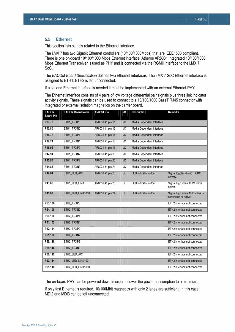
The Ethernet interface consists of 4 pairs of low voltage differential pair signals plus three link indicator activity signals. These signals can be used to connect to a 10/100/1000 BaseT RJ45 connector with integrated or external isolation magnetics on the carrier board.
EACOM Board Pin
EACOM Board Name AR8031 Pin I/O Description Remarks
P39/78 ETH1_TRXP0 AR8031 #1 pin 11 I/O Media Dependent Interface
P40/80 ETH1_TRXN0 AR8031 #1 pin 12 I/O Media Dependent Interface
P36/72 ETH1_TRXP1 AR8031 #1 pin 14 I/O Media Dependent Interface
P37/74 ETH1_TRXN1 AR8031 #1 pin 15 I/O Media Dependent Interface
P48/96 ETH1_TRXP2 AR8031 #1 pin 17 I/O Media Dependent Interface
P47/94 ETH1_TRXN2 AR8031 #1 pin 18 I/O Media Dependent Interface
P45/90 ETH1_TRXP3 AR8031 #1 pin 20 I/O Media Dependent Interface
P44/88 ETH1_TRXN3 AR8031 #1 pin 21 I/O Media Dependent Interface
P42/84 ETH1_LED_ACT AR8031 #1 pin 23 O LED indicator output Signal toggles during TX/RX activity.
P43/86 ETH1_LED_LINK AR8031 #1 pin 26 O LED indicator output Signal high when 100M link is active.
P41/82 ETH1_LED_LINK1000 AR8031 #1 pin 24 O LED indicator output Signal high when 1000M link is connected or active.
P53/106 ETH2_TRXP0 ETH2 interface not connected
P54/108 ETH2_TRXN0 ETH2 interface not connected
P50/100 ETH2_TRXP1 ETH2 interface not connected
P51/102 ETH2_TRXN1 ETH2 interface not connected
P62/124 ETH2_TRXP2 ETH2 interface not connected
P61/122 ETH2_TRXN2 ETH2 interface not connected
P59/118 ETH2_TRXP3 ETH2 interface not connected
P58/116 ETH2_TRXN3 ETH2 interface not connected
P56/112 ETH2_LED_ACT ETH2 interface not connected
P57/114 ETH2_LED_LINK100 ETH2 interface not connected
P55/110 ETH2_LED_LINK1000 ETH2 interface not connected
The on-board PHY can be powered down in order to lower the power consumption to a minimum.
If only fast Ethernet is required, 10/100Mbit magnetics with only 2 lanes are sufficient. In this case, MDI2 and MDI3 can be left unconnected.

iMX7 Dual COM Board - Datasheet Page 36
Copyright 2016 © Embedded Artists AB
Below is a list of suggested magnetics for 10/100/1000 Mbps Gigabit Ethernet operation:
Vendor P/N Package Temp Configuration
HanRun HR911060C Integrated RJ45 0 - 70° Celsius HP Auto-MDIX
Halo HFJ11-1G02E Integrated RJ45 0 - 70° Celsius HP Auto-MDIX
UDE RB1-BA6BT9WA Integrated RJ45 0 - 70° Celsius HP Auto-MDIX
Pulse Electronics (Recommended by Atheros)
H5007 24-pin SOIC-W 0 - 70° Celsius HP Auto-MDIX
Halo TG1G-S002NZRL 24-pin SOIC-W -40 - 85° Celsius HP Auto-MDIX
UDE RB1-BA6BT9WA Integrated RJ45 -40 - 85° Celsius HP Auto-MDIX
Halo TG1G-E012NZRL 24-pin SOIC-W -40 - 85° Celsius HP Auto-MDIX
5.5.1 Second Ethernet Interface
A second Ethernet interface can be implemented with an external Ethernet-PHY. See section 11.1 - Ethernet MAC (ENET) in the iMX7 Dual Reference Manual, document IMX7DRM.
The i.MX 7 supports the MII, RMII and RGMII interfaces and can be connected to any industry standard Ethernet-PHY. The table below lists the signals used when connecting to a second (external) Ethernet-PHY.
EACOM Board Pin
EACOM Board Name
i.MX 7 Ball Name I/O Description MII interface RMII interface RGMII interface
P92/192 COM specific EPDC1_PWRSTAT I Pin carry alternative signal ENET2_COL
MII_COL - -
P93/194 COM specific EPDC1_PWRCOM I Pin carry alternative signal ENET2_CRS
MII_CRS - -
P114/236 COM specific EPDC1_BDR1 I Pin carry alternative signal ENET2_RX_CLK
MII_RX_CLK - -
P115/238 COM specific EPDC1_BDR0 O Pin carry alternative signal ENET2_TX_CLK
MII_TX_CLK 50MHz ref clock
-
S52/103 TP_RST EPDC1_GDSP O Pin carry alternative signal ENET2_TX_ER
MII_TX_ER - RGMII_TXC
P96/200 COM specific EPDC1_SDCLK I Pin carry alternative signal RGMII2_RD0
MII_RD0 RMII_RXD0 RGMII_RXD0
P95/198 COM specific EPDC1_SDLE I Pin carry alternative signal RGMII2_RD1
MII_RD1 RMII_RXD1 RGMII_RXD1
P94/196 COM specific EPDC1_SDOE I Pin carry alternative signal RGMII2_RD2
MII_RD2 - RGMII_RXD2
S121/247 CSI_D2 EPDC1_SDSHR I Pin carry alternative signal RGMII2_RD3
MII_RD3 - RGMII_RXD3
P140/288 GPIO1 EPDC1_SDCE0 I Pin carry alternative signal RGMII2_RX_CTL
MII_RX_DV RMII_CRS_DV RGMII_RX_CTL
P139/286 GPIO2 EPDC1_SDCE1 I Pin carry alternative signal RGMII2_RXC
MII_RX_ER RMII_RXER RGMII_RXC
P2/4 GPIO5 EPDC1_SDCE2 O Pin carry alternative signal RGMII2_TD0
MII_TD0 RMII_TXD0 RGMII_TXD0
P1/2 GPIO6 EPDC1_SDCE3 O Pin carry alternative MII_TD1 RMII_TXD1 RGMII_TXD1

iMX7 Dual COM Board - Datasheet Page 37
Copyright 2016 © Embedded Artists AB
signal RGMII2_TD1
S55/109 BL_PWR_EN EPDC1_GDCLK O Pin carry alternative signal RGMII2_TD2
MII_TD2 - RGMII_TXD2
S54/107 DISP_PWR_EN EPDC1_GDOE O Pin carry alternative signal RGMII2_TD3
MII_TD3 - RGMII_TXD3
S53/105 TP_IRQ EPDC1_GDRL O Pin carry alternative signal RGMII2_TX_CTL
MII_TX_EN RMII_TXEN RGMII_TX_CTL
The MDIO interface is a two-wire management interface. The MDIO management interface implements a standardized method to access the PHY device management registers.
The two pins that are used for the on-board Ethernet-PHY are available for off-board access, see the first two rows in the table below. These can with advantage be used to control the external, off-board Ethernet-PHY. Alternatively, a second MDIO interface is also available, see row 3-8 in the table below.
EACOM Board Pin
EACOM Board Name
i.MX 7 Ball Name I/O Description Remarks
S116/237 CSI_MCLK GPIO1_IO10-ETH_PHY_MDIO
I/O Non-standard pin allocation.
Signal allocated for ETH_PHY_MDIO and used by on-board Ethernet-PHY. Signal can be used for external Ethernet-PHY for second Ethernet interface.
S115/235 CSI_VSYNC GPIO1_IO11/ ETH_PHY_MDC
O Non-standard pin allocation.
Signal allocated for ETH_PHY_MDC and used by on-board Ethernet-PHY. Signal can be used for external Ethernet-PHY for second Ethernet interface.
S12/23 CAN2_TX GPIO1_IO15 O Pin carry alternative signal ENET2_MDC
S124/253 CSI_D5 SD2_WP O Pin carry alternative signal ENET2_MDC
P133/274 UART-B_TXD UART2_TXD O Pin carry alternative signal ENET2_MDC
S13/25 CAN2_RX GPIO1_IO14 I/O Pin carry alternative signal ENET2_ MDIO
S122/249 CSI_D3 SD2_CD_B I/O Pin carry alternative signal ENET2_ MDIO
P130/268 UART-B_RXD UART2_RXD I/O Pin carry alternative signal ENET2_ MDIO
iMX7 Dual COM Board - Datasheet Page 38
Copyright 2016 © Embedded Artists AB
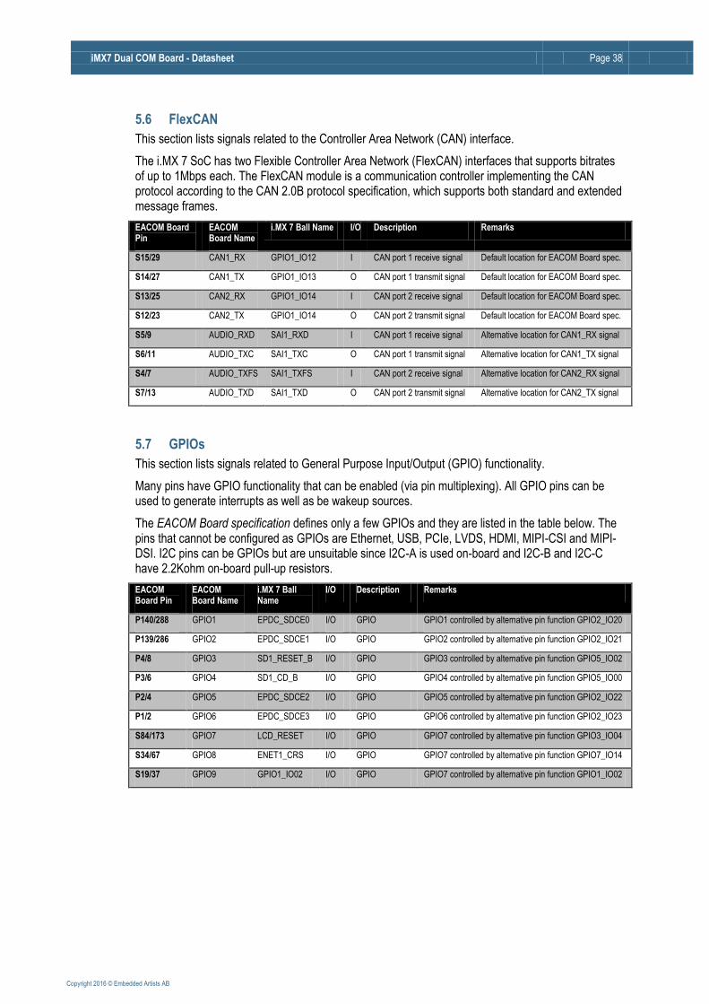
5.6 FlexCAN
This section lists signals related to the Controller Area Network (CAN) interface.
The i.MX 7 SoC has two Flexible Controller Area Network (FlexCAN) interfaces that supports bitrates of up to 1Mbps each. The FlexCAN module is a communication controller implementing the CAN protocol according to the CAN 2.0B protocol specification, which supports both standard and extended message frames.
EACOM Board Pin
EACOM Board Name
i.MX 7 Ball Name I/O Description Remarks
S15/29 CAN1_RX GPIO1_IO12 I CAN port 1 receive signal Default location for EACOM Board spec.
S14/27 CAN1_TX GPIO1_IO13 O CAN port 1 transmit signal Default location for EACOM Board spec.
S13/25 CAN2_RX GPIO1_IO14 I CAN port 2 receive signal Default location for EACOM Board spec.
S12/23 CAN2_TX GPIO1_IO14 O CAN port 2 transmit signal Default location for EACOM Board spec.
S5/9 AUDIO_RXD SAI1_RXD I CAN port 1 receive signal Alternative location for CAN1_RX signal
S6/11 AUDIO_TXC SAI1_TXC O CAN port 1 transmit signal Alternative location for CAN1_TX signal
S4/7 AUDIO_TXFS SAI1_TXFS I CAN port 2 receive signal Alternative location for CAN2_RX signal
S7/13 AUDIO_TXD SAI1_TXD O CAN port 2 transmit signal Alternative location for CAN2_TX signal
5.7 GPIOs
This section lists signals related to General Purpose Input/Output (GPIO) functionality.
Many pins have GPIO functionality that can be enabled (via pin multiplexing). All GPIO pins can be used to generate interrupts as well as be wakeup sources.
The EACOM Board specification defines only a few GPIOs and they are listed in the table below. The pins that cannot be configured as GPIOs are Ethernet, USB, PCIe, LVDS, HDMI, MIPI-CSI and MIPI-DSI. I2C pins can be GPIOs but are unsuitable since I2C-A is used on-board and I2C-B and I2C-C have 2.2Kohm on-board pull-up resistors.
EACOM Board Pin
EACOM Board Name
i.MX 7 Ball Name
I/O Description Remarks
P140/288 GPIO1 EPDC_SDCE0 I/O GPIO GPIO1 controlled by alternative pin function GPIO2_IO20
P139/286 GPIO2 EPDC_SDCE1 I/O GPIO GPIO2 controlled by alternative pin function GPIO2_IO21
P4/8 GPIO3 SD1_RESET_B I/O GPIO GPIO3 controlled by alternative pin function GPIO5_IO02
P3/6 GPIO4 SD1_CD_B I/O GPIO GPIO4 controlled by alternative pin function GPIO5_IO00
P2/4 GPIO5 EPDC_SDCE2 I/O GPIO GPIO5 controlled by alternative pin function GPIO2_IO22
P1/2 GPIO6 EPDC_SDCE3 I/O GPIO GPIO6 controlled by alternative pin function GPIO2_IO23
S84/173 GPIO7 LCD_RESET I/O GPIO GPIO7 controlled by alternative pin function GPIO3_IO04
S34/67 GPIO8 ENET1_CRS I/O GPIO GPIO7 controlled by alternative pin function GPIO7_IO14
S19/37 GPIO9 GPIO1_IO02 I/O GPIO GPIO7 controlled by alternative pin function GPIO1_IO02

iMX7 Dual COM Board - Datasheet Page 39
Copyright 2016 © Embedded Artists AB
5.8 I2C
This section lists signals related to the Inter-Integrated Circuit (I2C) interface.
The i.MX 7 SoC has four I2C interfaces. Three of these are assigned in the EACOM Board Specification. i.MX 7 I2C channel #1 is assigned to EACOM I2C channel A. I2C channel #2 is assigned to EACOM I2C channel B. I2C channel #3 is assigned to EACOM I2C channel C.
Pin assignment for I2C channel A cannot be changed since this channel is used on the iMX7 Dual COM board (for PMIC and E2PROM communication). It is recommended not to change pin assignment since for EACOM I2C channel B and C (I2C channel #2 and #3, respectively) since these four pins have 2.2Kohm pull-up resistors.
The table below lists the pin assignment as well as alternative pin locations.
EACOM Board Pin
EACOM Board Name
i.MX 7 Ball Name
I/O Description Remarks
S47/93 I2C-A_SCL I2C1_SCL I/O Clock signal of I2C channel #1
Signal has on-board 2.2Kohm pullup resistor. Signal is connected to on-board I2C channel to PMIC and E2PROM.
S46/91 I2C-A_SDA I2C1_SDA I/O Data signal of I2C channel #1
Signal has on-board 2.2Kohm pullup resistor. Signal is connected to on-board I2C channel to PMIC and E2PROM.
S49/97 I2C-B_SCL I2C2_SCL I/O Clock signal of I2C channel #2
Signal has on-board 2.2Kohm pullup resistor.
S48/95 I2C-B_SDA I2C2_SDA I/O Data signal of I2C channel #2
Signal has on-board 2.2Kohm pullup resistor.
S51/101 I2C-C_SCL I2C3_SCL I/O Clock signal of I2C channel #3
Signal has on-board 2.2Kohm pullup resistor.
S50/99 I2C-C_SDA I2C3_SDA I/O Data signal of I2C channel #3
Signal has on-board 2.2Kohm pullup resistor.
Note that the following two positions for I2C interfaces are not allowed:
I2C1_SCL on i.MX 7 pins GPIO1_IO04 and UART1_RXD should not be used. I2C
channel #1 is allocated on another pin.
I2C1_SDA on i.MX 7 pins GPIO1_IO05 and UART1_TXD should not be used. I2C
channel #1 is allocated on another pin.
i.MX 7 I2C interface #2 can are located on the following pins (as alternative functions), but note that these locations are not recommended since the EACOM Board specification has allocated this function on another pin, see above.
EACOM Board Pin
EACOM Board Name
i.MX 7 Ball Name
I/O Description Remarks
P76/160 USB_H1_OC GPIO1_IO06 I/O Clock signal of I2C channel #2
I2C2_SCL. Note that this location is not recommended since the EACOM Board specification has allocated this function on another pin, see above.
P130/268 UART-B_RXD UART2_RXD I/O Clock signal of I2C channel #2
I2C2_SCL. Note that this location is not recommended since the EACOM Board specification has allocated this function on another pin, see above.
P75/158 USB_H1_PWR_EN GPIO1_IO07 I/O Data signal of I2C channel #2
I2C2_SDA. Note that this location is not recommended since the EACOM Board specification has allocated this function on another pin, see above.
P133/274 UART-B_TXD UART2_TXD I/O Data signal of I2C channel #2
I2C2_SDA. Note that this location is not recommended since the EACOM Board specification has allocated this function on another pin, see above.

iMX7 Dual COM Board - Datasheet Page 40
Copyright 2016 © Embedded Artists AB
i.MX 7 I2C interface #3 can are located on the following pins (as alternative functions).
EACOM Board Pin
EACOM Board Name
i.MX 7 Ball Name I/O Description Remarks
P117/242 COM specific GPIO1_IO08 I/O Clock signal of I2C channel #3
I2C3_SCL. Note that this location is not recommended since the EACOM Board specification has allocated this function on another pin, see above.
S62/123 LCD_R4 LCD1_DATA20 I/O Clock signal of I2C channel #3
I2C3_SCL. Note that this location is not recommended since the EACOM Board specification has allocated this function on another pin, see above.
S117/239 CSI_PCLK GPIO1_IO09 I/O Data signal of I2C channel #3
I2C3_SDA. Note that this location is not recommended since the EACOM Board specification has allocated this function on another pin, see above.
S63/125 LCD_R5 LCD1_DATA21 I/O Data signal of I2C channel #3
I2C3_SDA. Note that this location is not recommended since the EACOM Board specification has allocated this function on another pin, see above.
i.MX 7 I2C interface #4 can are located on the following pins (as alternative functions).
EACOM Board Pin
EACOM Board Name
i.MX 7 Ball Name
I/O Description Remarks
S113/231 COM specific I2C4_SCL I/O Clock signal of I2C channel #4
Note that an external pull-up resistor is needed.
S116/237 CSI_MCLK GPIO1_IO10 I/O Clock signal of I2C channel #4
Note that an external pull-up resistor is needed.
S64/127 LCD_R6 LCD1_DATA22 I/O Clock signal of I2C channel #4
Note that an external pull-up resistor is needed.
S1/1 MQS_RIGHT SAI1_RXFS I/O Clock signal of I2C channel #4
Note that an external pull-up resistor is needed.
S112/229 COM specific I2C4_SDA I/O Data signal of I2C channel #4
Note that an external pull-up resistor is needed.
S115/235 CSI_VSYNC GPIO1_IO11 I/O Data signal of I2C channel #4
Note that an external pull-up resistor is needed.
S65/129 LCD_R7 LCD1_DATA23 I/O Data signal of I2C channel #4
Note that an external pull-up resistor is needed.
S2/3 MQS_LEFT SAI1_RXC I/O Data signal of I2C channel #4
Note that an external pull-up resistor is needed.

iMX7 Dual COM Board - Datasheet Page 41
Copyright 2016 © Embedded Artists AB
5.9 JTAG
This section lists signals related to the JTAG debug interface.
The i.MX 7 SoC has a module called System JTAG Controller (SJC) that provides a JTAG interface to internal logic, including the two ARM Cortex-A9 cores and Cortex-M4 core. The SJC complies with JTAG TAP standards. The i.MX 7 SoC use the JTAG port for production, testing, and system debugging.
The JTAG signals are not available on the MXM3 edge connector. Instead the signals are available via a 10 pos FPC connector, see picture below for location and orientation.
Figure 7 – iMX7 Dual COM Board, Top Side
The table below lists the 10 signals on the JTAG connector.
J1 Pin Number
Connected to i.MX 7 Ball Name
I/O Description Remarks
1 NVCC_JTAG O Logic level supply voltage Used by external debugger to detect logic level to use for signaling. Typically 3.3V.
2 JTAG_TMS I JTAG signal TMS
3 Ground
4 JTAG_TCK I JTAG signal TCK
5 Ground
6 JTAG_TDO O JTAG signal TDO
7 JTAG_MOD I Signal shall always be connected to ground. Signal has a 1Kohm pulldown resistor and can be left floating.
8 JTAG_TDI I JTAG signal TDI
9 JTAG_TRST I JTAG signal TRST
10 JTAG_SRST I System reset Signal is active low and controls internal system reset. Signal has a 10K ohm pullup resistor.
JTAG Interface Connector Pin 10 to 1 (top to bottom)

iMX7 Dual COM Board - Datasheet Page 42
Copyright 2016 © Embedded Artists AB
The iMX7 Dual Developer's Kit contains an adapter board for connection to common debug connectors. The 10 pos connector is Molex 512811094 and has 0.5 mm (20 mil) pitch. FPC length should be kept less than 7 cm.
5.10 PCI Express
This section lists signals related to the PCI Express interface.
The i.MX 7Dual SoC has a single lane PCI Express (PCIe) interface. The interface is compliant with the PCIe 2.1 specification that supports up to 6Gbit/s data rate. PCIe 2.1/2.0 is backward compatible with the PCIe 1.1 standard that supports 2.5Gbit/s data rate.
EACOM Board Pin
EACOM Board Name
i.MX 7 Ball Name I/O Description Remarks
S150/305 PCIE_CLK_P PCIE_REFCLKOUT_P O 100 MHz reference clock, positive signal in differential pair
S151/307 PCIE_CLK_N PCIE_REFCLKOUT_N O 100 MHz reference clock, negative signal in differential pair
S153/311 PCIE_TX_P PCIE_TX_P O Transmit data, positive signal in differential pair
S154/313 PCIE_TX_N PCIE_TX_N O Transmit data, negative signal in differential pair
S156/317 PCIE_RX_P PCIE_RX_P I Receive data, positive signal in differential pair
S157/319 PCIE_RX_N PCIE_RX_N I Receive data, negative signal in differential pair
S147/299 SATA_RX_P PCIE_REFCLKIN_P I If PCIe is used, connect to a 100MHz PCIe compatible reference clock with HCSL-signal output, positive signal
Non-standard pin allocation.
S146/297 SATA_RX_N PCIE_REFCLKIN_N I If PCIe is used, connect to a 100MHz PCIe compatible reference clock with HCSL-signal output, negative signal
Non-standard pin allocation.
A typical PCIe interface also has a USB Host, a I2C interface and (typically) three control signals; wakeup (input to iMX7), disable and reset (outputs from iMX7). These interfaces and control signals are not specifically defined in the EACOM Board specification and is up to each carrier board design to assign/allocate.
5.11 Power Management
This section lists signals related to power management, i.e., reset and external power supplies.
EACOM Board Pin
EACOM Board Name I/O Description Remarks
P143/294 RESET_OUT O Reset output, active low Open drain output. Driven low during reset. 1.5K pull-up resistor to VIN.
P142/292 RESET_IN I Reset input, active low Pull signal low to activate reset. No need to pull signal high externally. Connected to cathode of series diode, so logic level of driving signal can be anywhere between 1.5-5 V.
P141/290 PERI_PWR_EN O Enable signal (active high) for carrier board peripheral power supplies.
Uses RESET signal from the i.MX 7. More information about carrier board design can be found in EACOM Board specification.
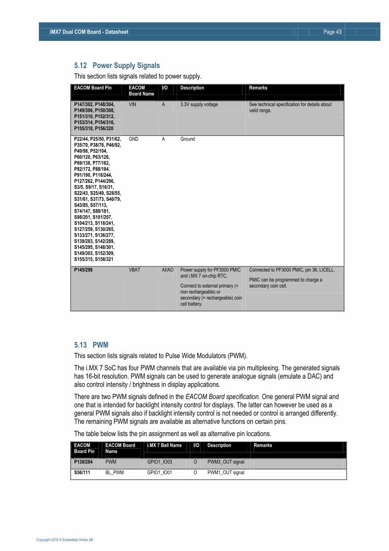
iMX7 Dual COM Board - Datasheet Page 43
Copyright 2016 © Embedded Artists AB
5.12 Power Supply Signals
This section lists signals related to power supply.
EACOM Board Pin EACOM Board Name
I/O Description Remarks
P147/302, P148/304, P149/306, P150/308, P151/310, P152/312, P153/314, P154/316, P155/318, P156/320
VIN A 3.3V supply voltage See technical specification for details about valid range.
P22/44, P25/50, P31/62, P35/70, P38/76, P46/92, P49/98, P52/104, P60/120, P63/126, P69/138, P77/162, P82/172, P88/184, P91/190, P118/244, P127/262, P144/296, S3/5, S9/17, S16/31, S22/43, S25/49, S28/55, S31/61, S37/73, S40/79, S43/85, S57/113, S74/147, S88/181, S98/201, S101/207, S104/213, S118/241, S127/259, S130/265, S133/271, S136/277, S139/283, S142/289, S145/295, S148/301, S149/303, S152/309, S155/315, S158/321
GND A Ground
P145/298 VBAT AI/AO Power supply for PF3000 PMIC and i.MX 7 on-chip RTC.
Connect to external primary (= non rechargeable) or secondary (= rechargeable) coin cell battery.
Connected to PF3000 PMIC, pin 36, LICELL.
PMIC can be programmed to charge a secondary coin cell.
5.13 PWM
This section lists signals related to Pulse Wide Modulators (PWM).
The i.MX 7 SoC has four PWM channels that are available via pin multiplexing. The generated signals has 16-bit resolution. PWM signals can be used to generate analogue signals (emulate a DAC) and also control intensity / brightness in display applications.
There are two PWM signals defined in the EACOM Board specification. One general PWM signal and one that is intended for backlight intensity control for displays. The latter can however be used as a general PWM signals also if backlight intensity control is not needed or control is arranged differently. The remaining PWM signals are available as alternative functions on certain pins.
The table below lists the pin assignment as well as alternative pin locations.
EACOM Board Pin
EACOM Board Name
i.MX 7 Ball Name I/O Description Remarks
P138/284 PWM GPIO1_IO03 O PWM3_OUT signal
S56/111 BL_PWM GPIO1_IO01 O PWM1_OUT signal

iMX7 Dual COM Board - Datasheet Page 44
Copyright 2016 © Embedded Artists AB
The table below lists the pin assignment for the alternative pin locations.
EACOM Board Pin
EACOM Board Name
i.MX 7 Ball Name I/O Description Remarks
P117/242 COM specific GPIO1_IO08 O PWM1_OUT signal
S19/37 GPIO9 GPIO1_IO02 O PWM2_OUT signal
S117/239 CSI_PCLK GPIO1_IO09 O PWM2_OUT signal
S116/237 CSI_MCLK GPIO1_IO10 O PWM3_OUT signal
S115/235 CSI_VSYNC GPIO1_IO11 O PWM4_OUT signal
5.14 SD/MMC
This section lists signals related to Ultra Secured Digital Host Controller (uSDHC) functions.
The i.MX 7 SoC has 3 uSDHC interfaces. One, uSDHC3, is allocated (on-board) for interface to eMMC Flash. The interfaces are capable of interfacing with SD Memory Cards, SDIO, MMC, CE-ATA cards and eMMC devices. The features of the uSDHC module include the following:
Conforms to the SD Host Controller Standard Specification version 3.0
Compatible with the MMC System Specification version 4.2/4.3/4.4/4.41/4.5/5.0
Compatible with the SD Memory Card Specification version 3.0 and supports the Extended Capacity SD Memory Card
Compatible with the SDIO Card Specification version 3.0
Designed to work with SD Memory, miniSD Memory, SDIO, miniSDIO, SD Combo, MMC, MMC plus, and MMC RS cards
Supports 1-bit / 4-bit SD and SDIO modes, 1-bit / 4-bit / 8-bit MMC modes
The EACOM Board specification defines one 4-databit SD interface (uSDHC1) and one 8-databit MMC interface (uSDHC2). The 8-bit MMC interface pin allocation is however only 4-bit.
The table below lists the pin assignment according to EACOM Board specification.
EACOM Board Pin
EACOM Board Name
i.MX 7 Ball Name I/O Description Remarks
P7/14 SD_CLK SD1_CLK O Clock for MMC/SD/SDIO card
P8/16 SD_CMD SD1_CMD I/O CMD line connect to card
P6/12 SD_D0 SD1_DATA0 I/O DATA0 line in all modes. Also used to detect busy status
P5/10 SD_D1 SD1_DATA1 I/O DATA1 line in 4/8-bit mode. Also used to detect interrupt in 1/4-bit mode
P10/20 SD_D2 SD1_DATA2 I/O DATA2 line or Read Wait in 4-bit mode, Read Wait in 1-bit mode
P9/18 SD_D3 SD1_DATA3 I/O DATA3 line in 4/8-bit mode or configured as card detection pin. May be configured as card detection pin in 1-bit mode
P16/32 MMC_CLK SD2_CLK O Clock for MMC/SD/SDIO card
P18/36 MMC_CMD SD2_CMD I/O CMD line connect to card
P13/26 MMC_D0 SD2_DATA0 I/O DATA0 line in all modes. Also used to detect busy status
P12/24 MMC_D1 SD2_DATA1 I/O DATA1 line in 4/8-bit mode Also used to detect interrupt in 1/4-bit mode
P10/20 MMC_D2 SD2_DATA2 I/O DATA2 line or Read Wait in 4-bit mode, Read Wait in 1-bit mode
P20/40 MMC_D3 SD2_DATA3 I/O DATA3 line in 4/8-bit mode or configured as card detection pin. May be configured as card detection pin in 1-bit mode
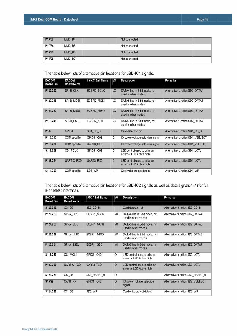
iMX7 Dual COM Board - Datasheet Page 45
Copyright 2016 © Embedded Artists AB
P19/38 MMC_D4 Not connected
P17/34 MMC_D5 Not connected
P15/30 MMC_D6 Not connected
P14/28 MMC_D7 Not connected
The table below lists of alternative pin locations for uSDHC1 signals.
EACOM Board Pin
EACOM Board Name
i.MX 7 Ball Name I/O Description Remarks
P122/252 SPI-B_CLK ECSPI2_SCLK I/O DATA4 line in 8-bit mode, not used in other modes
Alternative function SD2_DATA4
P120/248 SPI-B_MOSI ECSPI2_MOSI I/O DATA5 line in 8-bit mode, not used in other modes
Alternative function SD2_DATA5
P121/250 SPI-B_MISO ECSPI2_MISO I/O DATA6 line in 8-bit mode, not used in other modes
Alternative function SD2_DATA6
P119/246 SPI-B_SSEL ECSPI2_SS0 I/O DATA7 line in 8-bit mode, not used in other modes
Alternative function SD2_DATA7
P3/6 GPIO4 SD1_CD_B I Card detection pin Alternative function SD1_CD_B.
P117/242 COM specific GPIO1_IO08 O IO power voltage selection signal Alternative function SD1_VSELECT
P113/234 COM specific UART3_CTS O IO power voltage selection signal Alternative function SD1_VSELECT
S117/239 CSI_PCLK GPIO1_IO09 O LED control used to drive an external LED Active high
Alternative function SD1_LCTL
P128/264 UART-C_RXD UART3_RXD O LED control used to drive an external LED Active high
Alternative function SD1_LCTL
S111/227 COM specific SD1_WP I Card write protect detect Alternative function SD1_WP
The table below lists of alternative pin locations for uSDHC2 signals as well as data signals 4-7 (for full 8-bit MMC interface).
EACOM Board Pin
EACOM Board Name
i.MX 7 Ball Name I/O Description Remarks
S122/249 CSI_D3 SD2_CD_B I Card detection pin Alternative function SD2_CD_B
P126/260 SPI-A_CLK ECSPI1_SCLK I/O DATA4 line in 8-bit mode, not used in other modes
Alternative function SD2_DATA4
P124/256 SPI-A_MOSI ECSPI1_MOSI I/O DATA5 line in 8-bit mode, not used in other modes
Alternative function SD2_DATA5
P125/258 SPI-A_MISO ECSPI1_MISO I/O DATA6 line in 8-bit mode, not used in other modes
Alternative function SD2_DATA6
P123/254 SPI-A_SSEL ECSPI1_SS0 I/O DATA7 line in 8-bit mode, not used in other modes
Alternative function SD2_DATA7
S116/237 CSI_MCLK GPIO1_IO10 O LED control used to drive an external LED Active high
Alternative function SD2_LCTL
P129/266 UART-C_TXD UART3_TXD O LED control used to drive an external LED Active high
Alternative function SD2_LCTL
S123/251 CSI_D4 SD2_RESET_B O Alternative function SD2_RESET_B
S15/29 CAN1_RX GPIO1_IO12 O IO power voltage selection signal
Alternative function SD2_VSELECT
S124/253 CSI_D5 SD2_WP I Card write protect detect Alternative function SD2_WP
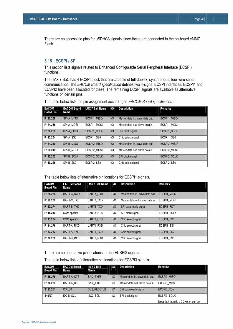
iMX7 Dual COM Board - Datasheet Page 46
Copyright 2016 © Embedded Artists AB
There are no accessible pins for uSDHC3 signals since these are connected to the on-board eMMC Flash.
5.15 ECSPI / SPI
This section lists signals related to Enhanced Configurable Serial Peripheral Interface (ECSPI) functions.
The i.MX 7 SoC has 4 ECSPI block that are capable of full-duplex, synchronous, four-wire serial communication. The EACOM Board specification defines two 4-signal ECSPI interfaces. ECSPI1 and ECSPI2 have been allocated for these. The remaining ECSPI signals are available as alternative functions on certain pins.
The table below lists the pin assignment according to EACOM Board specification.
EACOM Board Pin
EACOM Board Name
i.MX 7 Ball Name I/O Description Remarks
P125/258 SPI-A_MISO ECSPI1_MISO I/O Master data in, slave data out ECSPI1_MISO
P124/256 SPI-A_MOSI ECSPI1_MOSI I/O Master data out, slave data in ECSPI1_MOSI
P126/260 SPI-A_SCLK ECSPI1_SCLK I/O SPI clock signal ECSPI1_SCLK
P123/254 SPI-A_SS0 ECSPI1_SS0 I/O Chip select signal ECSPI1_SS0
P121/250 SPI-B_MISO ECSPI2_MISO I/O Master data in, slave data out ECSPI2_MISO
P120/248 SPI-B_MOSI ECSPI2_MOSI I/O Master data out, slave data in ECSPI2_MOSI
P122/252 SPI-B_SCLK ECSPI2_SCLK I/O SPI clock signal ECSPI2_SCLK
P119/246 SPI-B_SS0 ECSPI2_SS0 I/O Chip select signal ECSPI2_SS0
The table below lists of alternative pin locations for ECSPI1 signals.
EACOM Board Pin
EACOM Board Name
i.MX 7 Ball Name I/O Description Remarks
P128/264 UART-C_RXD UART3_RXD I/O Master data in, slave data out ECSPI1_MISO
P129/266 UART-C_TXD UART3_TXD I/O Master data out, slave data in ECSPI1_MOSI
P133/274 UART-B_TXD UART2_TXD I/O SPI data ready signal ECSPI1_RDY
P116/240 COM specific UART3_RTS I/O SPI clock signal ECSPI1_SCLK
P113/234 COM specific UART3_CTS I/O Chip select signal ECSPI1_SS0
P134/276 UART-A_RXD UART1_RXD I/O Chip select signal ECSPI1_SS1
P137/282 UART-A_TXD UART1_TXD I/O Chip select signal ECSPI1_SS2
P130/268 UART-B_RXD UART2_RXD I/O Chip select signal ECSPI1_SS3
There are no alternative pin locations for the ECSPI2 signals.
The table below lists of alternative pin locations for ECSPI3 signals.
EACOM Board Pin
EACOM Board Name
i.MX 7 Ball Name
I/O Description Remarks
P135/278 UART-A_CTS SAI2_TXFS I/O Master data in, slave data out ECSPI3_MISO
P136/280 UART-A_RTS SAI2_TXC I/O Master data out, slave data in ECSPI3_MOSI
S123/251 CSI_D4 SD2_RESET_B I/O SPI data ready signal ECSPI3_RDY
S49/97 I2C-B_SCL I2C2_SCL I/O SPI clock signal ECSPI3_SCLK
Note that there is a 2.2Kohm pull-up
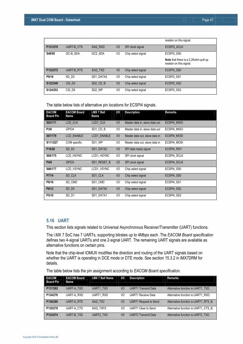
iMX7 Dual COM Board - Datasheet Page 47
Copyright 2016 © Embedded Artists AB
resistor on this signal.
P131/270 UART-B_CTS SAI2_RXD I/O SPI clock signal ECSPI3_SCLK
S48/95 I2C-B_SDA I2C2_SDA I/O Chip select signal ECSPI3_SS0
Note that there is a 2.2Kohm pull-up resistor on this signal.
P132/272 UART-B_RTS SAI2_TXD I/O Chip select signal ECSPI3_SS0
P9/18 SD_D3 SD1_DATA3 I/O Chip select signal ECSPI3_SS1
S122/249 CSI_D3 SD2_CD_B I/O Chip select signal ECSPI3_SS2
S124/253 CSI_D5 SD2_WP I/O Chip select signal ECSPI3_SS3
The table below lists of alternative pin locations for ECSPI4 signals.
EACOM Board Pin
EACOM Board Name
i.MX 7 Ball Name
I/O Description Remarks
S83/171 LCD_CLK LCD1_CLK I/O Master data in, slave data out ECSPI4_MISO
P3/6 GPIO4 SD1_CD_B I/O Master data in, slave data out ECSPI4_MISO
S87/179 LCD_ENABLE LCD1_ENABLE I/O Master data out, slave data in ECSPI4_MOSI
S111/227 COM specific SD1_WP I/O Master data out, slave data in ECSPI4_MOSI
P10/20 SD_D2 SD1_DATA2 I/O SPI data ready signal ECSPI4_RDY
S85/175 LCD_HSYNC LCD1_HSYNC I/O SPI clock signal ECSPI4_SCLK
P4/8 GPIO3 SD1_RESET_B I/O SPI clock signal ECSPI4_SCLK
S86/177 LCD_VSYNC LCD1_VSYNC I/O Chip select signal ECSPI4_SS0
P7/14 SD_CLK SD1_CLK I/O Chip select signal ECSPI4_SS0
P8/16 SD_CMD SD1_CMD I/O Chip select signal ECSPI4_SS1
P6/12 SD_D0 SD1_DATA0 I/O Chip select signal ECSPI4_SS2
P5/10 SD_D1 SD1_DATA1 I/O Chip select signal ECSPI4_SS3
5.16 UART
This section lists signals related to Universal Asynchronous Receiver/Transmitter (UART) functions.
The i.MX 7 SoC has 7 UARTs, supporting bitrates up to 4Mbps each. The EACOM Board specification defines two 4-signal UARTs and one 2-signal UART. The remaining UART signals are available as alternative functions on certain pins.
Note that the chip-level IOMUX modifies the direction and routing of the UART signals based on whether the UART is operating in DCE mode or DTE mode. See section 15.3.2 in IMX7DRM for details.
The table below lists the pin assignment according to EACOM Board specification.
EACOM Board Pin
EACOM Board Name
i.MX 7 Ball Name I/O Description Remarks
P137/282 UART-A_TXD UART1_TXD I/O UART1 Transmit Data Alternative function is UART1_TXD.
P134/276 UART-A_RXD UART1_RXD I/O UART1 Receive Data Alternative function is UART1_RXD.
P136/280 UART-A_RTS SAI2_TXC I/O UART1 Request to Send Alternative function is UART1_RTS_B.
P135/278 UART-A_CTS SAI2_TXFS I/O UART1 Clear to Send Alternative function is UART1_CTS_B.
P133/274 UART-B_TXD UART2_TXD I/O UART2 Transmit Data Alternative function is UART2_TXD.

iMX7 Dual COM Board - Datasheet Page 48
Copyright 2016 © Embedded Artists AB
P130/268 UART-B_RXD UART2_RXD I/O UART2 Receive Data Alternative function is UART2_RXD.
P132/272 UART-B_RTS SAI2_TXD I/O UART2 Request to Send Alternative function is UART2_RTS_B.
P131/270 UART-B_CTS SAI2_RXD I/O UART2 Clear to Send Alternative function is UART2_CTS_B.
P129/266 UART-C_TXD UART3_TXD I/O UART3 Transmit Data Alternative function is UART3_TXD.
P128/264 UART-C_RXD UART3_RXD I/O UART3 Receive Data Alternative function is UART3_RXD.
There are no alternative pin locations for UART1 signals.
The table below lists of alternative pin locations for UART2 signals.
EACOM Board Pin
EACOM Board Name
i.MX 7 Ball Name I/O Description Remarks
S87/179 LCD_ENABLE LCD1_ENABLE I/O UART2 Transmit Data Alternative function is UART2_TXD.
S83/171 LCD_CLK LCD1_CLK I/O UART2 Receive Data Alternative function is UART2_RXD.
S85/175 LCD_HSYNC LCD1_HSYNC I/O UART2 Request to Send Alternative function is UART2_RTS_B.
S86/177 LCD_VSYNC LCD1_VSYNC I/O UART2 Clear to Send Alternative function is UART2_CTS_B.
The table below lists of alternative pin locations for UART3 signals.
EACOM Board Pin
EACOM Board Name
i.MX 7 Ball Name I/O Description Remarks
S117/239 CSI_PCLK GPIO1_IO09 I/O UART3 Transmit Data Alternative function is UART3_TXD.
P117/242 COM specific GPIO1_IO08 I/O UART3 Receive Data Alternative function is UART3_RXD.
S116/237 CSI_MCLK GPIO1_IO10 I/O UART3 Request to Send Alternative function is UART3_RTS_B.
P116/240 COM specific UART3_RTS I/O UART3 Request to Send Alternative function is UART3_RTS_B.
S115/235 CSI_VSYNC GPIO1_IO11 I/O UART3 Clear to Send Alternative function is UART3_CTS_B.
P113/234 COM specific UART3_CTS I/O UART3 Clear to Send Alternative function is UART3_CTS_B.
The table below lists of alternative pin locations for UART4 signals.
EACOM Board Pin
EACOM Board Name
i.MX 7 Ball Name I/O Description Remarks
S48/95 I2C-B_SDA I2C2_SDA I/O UART4 Transmit Data Alternative function is UART4_TXD.
Note that there is a 2.2Kohm pull-up resistor on this signal.
P136/280 UART-A_RTS SAI2_TXC I/O UART4 Transmit Data Alternative function is UART4_TXD.
P12/24 MMC_D1 SD2_DATA1 I/O UART4 Transmit Data Alternative function is UART4_TXD.
S49/97 I2C-B_SCL I2C2_SCL I/O UART4 Receive Data Alternative function is UART4_RXD.
Note that there is a 2.2Kohm pull-up resistor on this signal.
P135/278 UART-A_CTS SAI2_TXFS I/O UART4 Receive Data Alternative function is UART4_RXD.
P13/26 MMC_D0 SD2_DATA0 I/O UART4 Receive Data Alternative function is UART4_RXD.
P132/272 UART-B_RTS SAI2_TXD I/O UART4 Request to Send Alternative function is UART4_RTS_B.
P20/40 MMC_D3 SD2_DATA3 I/O UART4 Request to Send Alternative function is UART4_RTS_B.
P131/270 UART-B_CTS SAI2_RXD I/O UART4 Clear to Send Alternative function is UART4_CTS_B.
P21/42 MMC_D2 SD2_DATA2 I/O UART4 Clear to Send Alternative function is UART4_CTS_B.

iMX7 Dual COM Board - Datasheet Page 49
Copyright 2016 © Embedded Artists AB
The table below lists of alternative pin locations for UART5 signals.
EACOM Board Pin
EACOM Board Name
i.MX 7 Ball Name I/O Description Remarks
P75/158 USB_H1_PWR_EN GPIO1_IO07 I/O UART5 Transmit Data Alternative function is UART5_TXD.
S112/229 COM specific I2C4_SDA I/O UART5 Transmit Data Alternative function is UART5_TXD.
S6/11 AUDIO_TXC SAI1_TXC I/O UART5 Transmit Data Alternative function is UART5_TXD.
P76/160 USB_H1_OC GPIO1_IO06 I/O UART5 Receive Data Alternative function is UART5_RXD.
S113/231 COM specific I2C4_SCL I/O UART5 Receive Data Alternative function is UART5_RXD.
S5/9 AUDIO_RXD SAI1_RXD I/O UART5 Receive Data Alternative function is UART5_RXD.
S7/13 AUDIO_TXD SAI1_TXD I/O UART5 Request to Send Alternative function is UART5_RTS_B.
S50/99 HDMI/I2C-C_SDA I2C3_SDA I/O UART5 Request to Send Alternative function is UART5_RTS_B.
Note that there is a 2.2Kohm pull-up resistor on this signal.
P73/146 USB_O1_PWR_EN GPIO1_IO05 I/O UART5 Request to Send Alternative function is UART5_RTS_B.
S4/7 AUDIO_TXFS SAI1_TXFS I/O UART5 Clear to Send Alternative function is UART5_CTS_B.
S51/101 HDMI/I2C-C_SCL I2C3_SCL I/O UART5 Clear to Send Alternative function is UART5_CTS_B.
Note that there is a 2.2Kohm pull-up resistor on this signal.
P74/148 USB_O1_OC GPIO1_IO04 I/O UART5 Clear to Send Alternative function is UART5_CTS_B.
The table below lists of alternative pin locations for UART6 signals.
EACOM Board Pin
EACOM Board Name
i.MX 7 Ball Name I/O Description Remarks
P124/256 SPI-A_MOSI ECSPI1_MOSI I/O UART6 Transmit Data Alternative function is UART6_TXD.
P103/214 COM specific EPDC1_DATA09 I/O UART6 Transmit Data Alternative function is UART6_TXD.
S111/227 COM specific SD1_WP I/O UART6 Transmit Data Alternative function is UART6_TXD.
P126/260 SPI-A_CLK ECSPI1_SCLK I/O UART6 Receive Data Alternative function is UART6_RXD.
P104/216 COM specific EPDC1_DATA08 I/O UART6 Receive Data Alternative function is UART6_RXD.
P3/6 GPIO4 SD1_CD_B I/O UART6 Receive Data Alternative function is UART6_RXD.
P125/258 SPI-A_MISO ECSPI1_MISO I/O UART6 Request to Send Alternative function is UART6_RTS_B.
P102/212 COM specific EPDC1_DATA10 I/O UART6 Request to Send Alternative function is UART6_RTS_B.
P4/8 GPIO3 SD1_RESET_B I/O UART6 Request to Send Alternative function is UART6_RTS_B.
P123/254 SPI-A_SSEL ECSPI1_SS0 I/O UART6 Clear to Send Alternative function is UART6_CTS_B.
P101/210 COM specific EPDC1_DATA11 I/O UART6 Clear to Send Alternative function is UART6_CTS_B.
P7/14 SD_CLK SD1_CLK I/O UART6 Clear to Send Alternative function is UART6_CTS_B.
The table below lists of alternative pin locations for UART7 signals.
EACOM Board Pin
EACOM Board Name
i.MX 7 Ball Name I/O Description Remarks
P120/248 SPI-B_MOSI ECSPI2_MOSI I/O UART7 Transmit Data Alternative function is UART7_TXD.
P99/206 COM specific EPDC1_DATA13 I/O UART7 Transmit Data Alternative function is UART7_TXD.
P5/10 SD_D1 SD1_DATA1 I/O UART7 Transmit Data Alternative function is UART7_TXD.
P122/252 SPI-B_CLK ECSPI2_SCLK I/O UART7 Receive Data Alternative function is UART7_RXD.

iMX7 Dual COM Board - Datasheet Page 50
Copyright 2016 © Embedded Artists AB
P100/208 COM specific EPDC1_DATA12 I/O UART7 Receive Data Alternative function is UART7_RXD.
P6/12 SD_D0 SD1_DATA0 I/O UART7 Receive Data Alternative function is UART7_RXD.
P121/250 SPI-B_MISO ECSPI2_MISO I/O UART7 Request to Send Alternative function is UART7_RTS_B.
P98/204 COM specific EPDC1_DATA14 I/O UART7 Request to Send Alternative function is UART7_RTS_B.
P9/18 SD_D3 SD1_DATA3 I/O UART7 Request to Send Alternative function is UART7_RTS_B.
P119/246 SPI-B_SSEL ECSPI2_SS0 I/O UART7 Clear to Send Alternative function is UART7_CTS_B.
P97/202 COM specific EPDC1_DATA15 I/O UART7 Clear to Send Alternative function is UART7_CTS_B.
P10/20 SD_D2 SD1_DATA2 I/O UART7 Clear to Send Alternative function is UART7_CTS_B.
5.17 USB
This section lists signals related to the USB interfaces.
The EACOM Board Specification has one USB 3.0 OTG port, one USB 3.0 Host port and one USB 2.0 Host port. The i.MX 7 has two USB 2.0 OTG ports and one HSIC port. Further, USB 3.0 is backward compatible with USB 2.0. The pins that are specific for USB 3.0 are just left unconnected and are for future upgrade.
The carrier board must provide a +5V supply (with enable and over-current functionality) for USB Host interfaces.
EACOM Board Pin
EACOM Board Name i.MX 7 Ball Name I/O Description Remarks
P64/128 USB_O1_DN USB_OTG1_DN I/O Negative Differential USB Signal, OTG compatible
P65/130 USB_O1_DP USB_OTG1_DP I/O Positive Differential USB Signal, OTG compatible
P66/132 USB_O1_ID USB_OTG1_ID I USB OTG ID pin
P67/134 USB_O1_SSTXN Not connected
P68/136 USB_O1_SSTXP Not connected
P70/140 USB_O1_SSRXN Not connected
P71/142 USB_O1_SSRXP Not connected
P72/144 USB_O1_VBUS USB_OTG1_VBUS I +5V USB VBUS detect input This pin is +5V tolerant.
P73/146 USB_O1_PWR_EN GPIO1_IO05 O Enable external USB voltage supply. Active high output.
Alternative function is USB_OTG1_PWR
P74/148 USB_O1_OC GPIO1_IO04 I Signals an over-current condition on the USB voltage supply. Active low input.
Alternative function is USB_OTG1_OC
P75/158 USB_H1_PWR_EN GPIO1_IO07 O Enable external USB voltage supply. Active high output.
Alternative function is USB_OTG2_PWR
P76/160 USB_H1_OC GPIO1_IO06 I Signals an over-current condition on the USB voltage supply. Active low input.
Alternative function is USB_OTG2_OC
P78/164 USB_H1_DN USB_OTG2_DN I/O Negative Differential USB Signal
P79/166 USB_H1_DP USB_OTG2_DP I/O Positive Differential USB Signal
P80/168 USB_H1_SSTXN Not connected
P81/170 USB_H1_SSTXP USB_OTG2_ID I/O Not standard pin allocation. Signal can optionally be used to create a OTG port of the EACOM USB Host post.
P83/174 USB_H1_SSRXN SNVS_TAMPER2 I/O Not standard pin allocation. Not connected for USB

iMX7 Dual COM Board - Datasheet Page 51
Copyright 2016 © Embedded Artists AB
functionality
P84/176 USB_H1_SSRXP SNVS_TAMPER1 I/O Not standard pin allocation. Not connected for USB functionality
P85/178 USB_H1_VBUS USB_OTG2_VBUS I +5V USB VBUS detect input This pin is +5V tolerant.
The table below lists of alternative pin locations for USB signals.
EACOM Board Pin
EACOM Board Name
i.MX 7 Ball Name I/O Description Remarks
S19/37 GPIO9 GPIO1_IO02 I USB OTG1 ID Alternative function is USB OTG1 ID
S15/29 CAN1_RX GPIO1_IO12 I USB OTG1 ID Alternative function is USB OTG1 ID
S113/231 COM specific I2C4_SCL I USB OTG1 ID Alternative function is USB OTG1 ID
S124/253 CSI_D5 SD2_WP I USB OTG1 ID Alternative function is USB OTG1 ID
P128/264 UART-C_RXD UART3_RXD I USB OTG1 OC Signals an over-current condition on the USB voltage supply. Active low input.
P129/266 UART-C_TXD UART3_TXD O USB OTG1 PWR EN Enable external USB voltage supply. Active high output.
P138/284 PWM GPIO1_IO03 I USB OTG2 ID Alternative function is USB OTG2 ID
S14/27 CAN1_TX GPIO1_IO13 I USB OTG2 ID Alternative function is USB OTG2 ID
S112/229 COM specific I2C4_SDA I USB OTG2 ID Alternative function is USB OTG2 ID
S123/251 CSI_D4 SD2_RESET_B I USB OTG2 ID Alternative function is USB OTG2 ID
P116/240 COM specific UART3_RTS I USB OTG2 OC Signals an over-current condition on the USB voltage supply. Active low input.
P113/234 COM specific UART3_CTS O USB OTG2 PWR EN Enable external USB voltage supply. Active high output.
Note that EACOM USB Host port #2 is connected to the High-Speed Inter-Chip (HSIC) interface on the i.MX 7. Some other signals are connected to these pins in a non-standard way, see table below.
EACOM Board Pin
EACOM Board Name
i.MX 7 Ball Name I/O Description Remarks
P86/180 USB_H2_PWR_EN SNVS_TAMPER0 signal, i.MX 7 ball AA7
I Not connected for USB functionality
Not standard pin allocation.
P87/182 USB_H2_OC ONOFF signal, i.MX 7 ball AC8
Not connected for USB functionality
Not standard pin allocation.
P89/186 USB_H2_DN HSIC_STROBE I/O HSIC strobe signal Not standard pin allocation.
P90/188 USB_H2_DP HSIC_DATA I/O HSIC data signal Not standard pin allocation.

iMX7 Dual COM Board - Datasheet Page 52
Copyright 2016 © Embedded Artists AB
6 Boot Options This chapter presents the different boot settings that the iMX7 Dual COM Board supports. This chapter will only present how the different options are controlled. Other documents discuss the pros and cons with different options and what general system architectures (with different booting phases) that are suitable in different situations.
The iMX7Dual COM Board supports booting (i.e., from where the i.MX 7Dual SoC starts downloading code to start executing from) from different sources:
1. On-board eMMC Flash (signal E2PROM_WP high/floating - default)
2. USB OTG download (also called 'serial download'), (signal E2PROM_WP low)
3. Other sources, like QSPI memory, external SD/MMC memory cards, etc. Note that the OTP fuses must be programmed to set these sources, see below.
Signal E2PROM_WP controls the booting source. If signal E2PROM_WP is high/floating, which is the default, booting takes place from eMMC. If Signal EPROM_WP is low, the i.MX 7Dual SoC boots into USB OTG mode. This latter mode it typically only used during production when the program images shall be downloaded the first time.
There are three main boot modes that controls which boot source to use.
1. Boot according to on-board configuration pull-up/pull-down resistors
- eMMC is set as default boot source.
- Note that signals LCD1_DATA00 - LCD1_DATA19 (EACOM pins LCD_B0-B7, LCD_G0-G7, LCD_R0-R3) must not be driven externally. This is normally not a problem since these signals are typically used for a parallel RGB display output. There are often driving buffers between these pins and an external display. The reason why the pins must not be driven externally is that on-board resistors pull these signals high/low to select eMMC booting. Driving any of these signals can change this default behavior. If any of the signals are driven externally the on-chip OTP fuses must be programmed to force eMMC booting instead.
2. Boot from USB OTG interface
- This mode is used in production to download the first stage bootloader and is typically not used by iMX7 Dual COM Board integrators. Sometimes this mode is called "Recovery mode".
- This mode is activated by pulling signal E2PROM_WP low.
3. Boot according to how internal (i.MX 7Dual on-chip) OTP fuses have been programmed
- Any boot mode supported by the i.MX 7Dual SoC and the hardware connected to it can be selected. See i.MX7 Dual Applications Processor Reference Manual for details about available sources and OTP fuse settings.
- Note that OTP fuse BT_FUSE_SEL must be set to 1 in order to override the default setting to boot from eMMC and to have OTP fuse settings controlling boot source instead.
- Note that the iMX7 Dual COM Boards have not programmed the on-chip OTP fuses. Users have full control over these. This mode can only be used after having programmed the OTP fuses.
- Programming OTP fuses is a critical operation. If wrong fuses are programmed boards will likely become unusable and there is no recovery.

iMX7 Dual COM Board - Datasheet Page 53
Copyright 2016 © Embedded Artists AB
To summarize, the iMX7 Dual COM board is setup to boot from eMMC as default. If another source is needed, program the OTP fuses.
If using the default setup (boot from eMMC), make sure the boot control pins (LCD1_DATA00 - LCD1_DATA19, which are the EACOM pins LCD_B0-B7, LCD_G0-G7, LCD_R0-R3) are not driven externally.
An optional USB OTG boot mode can be enabled by pulling signal E2PROM_WP low.

iMX7 Dual COM Board - Datasheet Page 54
Copyright 2016 © Embedded Artists AB
7 Power Modes One of the primary features of the i.MX7 SoC is low power consumption. The iMX7 Dual COM Board supports these features in the design. There are several different power modes that gives varying trade-offs between active functionality and power consumption. The table below lists, from lowest to highest power consumption, the available mode. There are three different versions of what is called the Low Power mode. These are variations on the basic mode.
Note that software support for these power modes vary between BSPs.
Mode Description DRAM state
Off All power rails are off Off
SNVS (RTC only) Only RTC and tamper detection logic is active Off
LPSR Low Power State Retention mode: This is an extension of the SNVS mode. All digital/analog modules are powered down but 16 GPIOs are also active for wakeup.
Off or DRAM stay in self-refresh, controlled by SW, pin SNVS_TAMPER9.
Low Power: Deep Sleep or Suspend
CPU power gated, most of the peripherals are power gated. All system clock shut off.
DRAM stay in self-refresh.
Low Power: Low Power Idle
CPU power gated, most of the peripherals are clock gated. Timer or other low speed peripheral can be running at 1MHz clock.
DRAM stay in self-refresh.
Low Power: System Idle
CPU automatically clock gated when in WFI state. Most of the peripherals remain active and running at 24MHz clock.
DRAM stay in self-refresh.
RUN All external power rails are on, CPU is active and running, other internal module can be on/off based on application
DRAM stay in self-refresh.
Valid power modes transitions are presented in the state machine diagram below.
Figure 8 – i.MX7 Power Modes Transitions
OFF
SNVS (RTC only)
RUN
LPSR
Low Power
RTC_VBAT supply present SW: Low Power request
Wake event (RTC, IRQ, tamper, etc)
ONOFF press or wake event (GPIO, RTC, IRQ, tamper, etc)
SW: LPSR sleep request
RTC_VBAT supply not present
ONOFF press, RTC or tamper event
SW, ONOFF long press or remove 3.3V VIN

iMX7 Dual COM Board - Datasheet Page 55
Copyright 2016 © Embedded Artists AB
The table below presents the different power supply voltage rails and their state in different power modes.
Power Rail Off SVNS (RTC only)
LPSR Low Power
Run
VDD_ARM (CPU cores) OFF OFF OFF ON/OFF ON
VDD_SOC OFF OFF OFF ON ON
VDD_DRAM OFF OFF ON/OFF ON ON
On-board Ethernet PHY OFF OFF OFF ON/OFF ON/OFF
Off-board peripherals controlled by PERI_PWR_EN
OFF OFF OFF ON ON
LPSR I/O OFF OFF ON ON ON
3.3V VIN OFF OFF ON ON ON
RTC_VBAT OFF ON ON ON ON
The different power modes are presented in more detail below.
7.1 Power Mode: OFF
This mode is self explanatory; all power rails are off.
7.2 Power Mode: SNVS (RTC only)
In this mode, only the RTC_VBAT power rail is on. All other power rails are off. The on-board Real-Time Clock (RTC) is running, i.e., keeping track of time.
Note that the power consumption of the RTC can quickly drain a standard (lithium) coin cell. A rechargeable battery solution is recommended. If this is not an option, an ultra-low power RTC (few uA) can be placed on the carrier board instead. In case, the RTC_VBAT power rail shall be connected to the 3.3V VIN power rail.
7.3 Power Mode: LPSR
This mode is an extension of the SNVS (RTC only) mode. In this state, the 3.3V VIN power rail is on but the CPUs and all digital/analog modules are powered down. IO rails are also off. The 16 LPSR IO pins are however active in this mode. One of the LPSR pins is used internally on the board (for watchdog functionality) but 15 LPSR IO pins are available for external expansion. These pins (GPIO1_IO01 - GPIO1_IO15) will keep their state in the LPSR mode and can be used to wake up the system again.
The DDR3L DRAM can optionally be kept in self-refresh mode, else it is switched off. Pin SNVS_TAMPER9 controls the self-refresh mode. A low pin level keeps the DRAM in self-refresh. A high pin level shuts down the DRAM.
7.4 Power Modes: Low Power
In this mode, the CPU is not running but the DRAM stays in self-refresh mode. There are three variations with different levels of power save and resulting response times.
Suspend/Deep Sleep
This is the lowest power consumption mode of the three. All clocks and peripherals that are
not used are turned off. Exiting this mode take the longest of these three modes.

iMX7 Dual COM Board - Datasheet Page 56
Copyright 2016 © Embedded Artists AB
Low Power Idle
In this mode, some peripherals blocks are active and some are not. The time to exiting this
mode is between the other two modes.
System Idle
This is the highest power consumption mode of the three. This mode can be entered
automatically if there is no system activity (i.e., no thread running). When entering this mode,
the peripheral blocks that shall still be active are defined. Exiting this mode is the fastest of
the three modes, resulting in short interrupt response.
7.5 Power Mode: RUN
In this mode, the system is up and running. All power rails are on. Functionality, like the Ethernet PHY, can be controlled via software to save power. The VDD_ARM (core voltage) can be adjusted via Dynamic Voltage Frequency Scaling (DVFS) techniques to reduce power consumption slightly. Basically, if the system load is low, the core operating frequency can be reduced and this allows the core voltage to also be reduced.
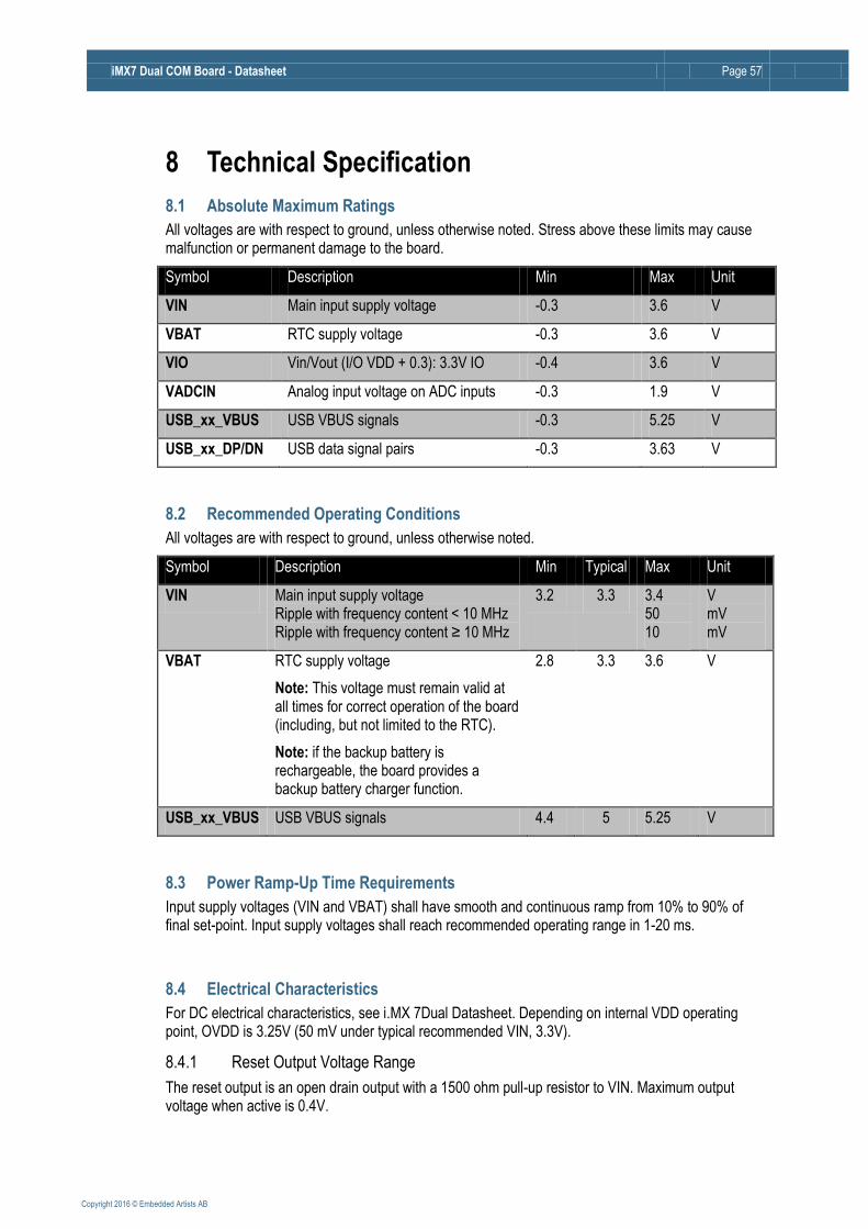
iMX7 Dual COM Board - Datasheet Page 57
Copyright 2016 © Embedded Artists AB
8 Technical Specification
8.1 Absolute Maximum Ratings
All voltages are with respect to ground, unless otherwise noted. Stress above these limits may cause malfunction or permanent damage to the board.
Symbol Description Min Max Unit
VIN Main input supply voltage -0.3 3.6 V
VBAT RTC supply voltage -0.3 3.6 V
VIO Vin/Vout (I/O VDD + 0.3): 3.3V IO -0.4 3.6 V
VADCIN Analog input voltage on ADC inputs -0.3 1.9 V
USB_xx_VBUS USB VBUS signals -0.3 5.25 V
USB_xx_DP/DN USB data signal pairs -0.3 3.63 V
8.2 Recommended Operating Conditions
All voltages are with respect to ground, unless otherwise noted.
Symbol Description Min Typical Max Unit
VIN Main input supply voltage Ripple with frequency content < 10 MHz Ripple with frequency content ≥ 10 MHz
3.2 3.3 3.4 50 10
V mV mV
VBAT RTC supply voltage
Note: This voltage must remain valid at all times for correct operation of the board (including, but not limited to the RTC).
Note: if the backup battery is rechargeable, the board provides a backup battery charger function.
2.8 3.3 3.6 V
USB_xx_VBUS USB VBUS signals 4.4 5 5.25 V
8.3 Power Ramp-Up Time Requirements
Input supply voltages (VIN and VBAT) shall have smooth and continuous ramp from 10% to 90% of final set-point. Input supply voltages shall reach recommended operating range in 1-20 ms.
8.4 Electrical Characteristics
For DC electrical characteristics, see i.MX 7Dual Datasheet. Depending on internal VDD operating point, OVDD is 3.25V (50 mV under typical recommended VIN, 3.3V).
8.4.1 Reset Output Voltage Range
The reset output is an open drain output with a 1500 ohm pull-up resistor to VIN. Maximum output voltage when active is 0.4V.

iMX7 Dual COM Board - Datasheet Page 58
Copyright 2016 © Embedded Artists AB
8.4.2 Reset Input
The reset input is triggered by pulling the reset input low (0.2 V max) for 20 uS minimum. The internal reset pulse will be 140-280 mS long, before the i.MX 7Dual boot process starts.
8.5 Power Consumption
There are several factors that determine power consumption of the iMX7 Dual COM Board, like input voltage, operating temperature, DDR3L activity, operating frequencies for the different cores, DVFS levels and software executed (i.e., Linux distribution).
The values presented are typical values and should be regarded as an estimate. Always measure current consumption in the real system to get a more accurate estimate.
Symbol Description (VIN = 3.3V, Toperating = 25°C) Typical Max Observed
Unit
IVIN_MAX Maximum CPU load, 996MHz ARM frequency, without Ethernet
360 mA
IVIN_IDLE System idle state, uBoot prompt Linux prompt, without Ethernet Linux prompt, with Ethernet
175 172 300
mA
IVIN_DSM Deep-Sleep mode (DSM), aka "Dormant mode" or "Suspend-to-RAM" in Linux BSP
40 mA
IVIN_STB Linux standby 43 mA
IVBAT_BACKUP Current consumption to keep internal RTC running
116 uA
IVIN_A7ACT Android 7 Desktop active 190 267 mA
IVIN_A7OFF Android 7 Display off 41 mA
8.6 Mechanical Dimensions
The board use the SMARC mechanical form factor.
Dimension Value (±0.1 mm) Unit
Module width 82 mm
Module height 50 mm
Module top side height 3.0 mm
Module bottom side height 1.3 mm
PCB thickness 1.2 mm
Mounting hole diameter
Note: This measurement is not identical with SMARC specification.
3.2 mm
Module weight 16 ±1 gram gram

iMX7 Dual COM Board - Datasheet Page 59
Copyright 2016 © Embedded Artists AB
The picture below show the mechanical details of the 82 x 50 mm module, including the pin numbering and edge finger pattern. The picture comes from the SMARC HW specification and show pin numbering in the Px and Sx format.
Picture source: SMARC HW Specification V1.1 © 2014 SGeT e.V.
4X ø3.2
THROUGH
4X ø6
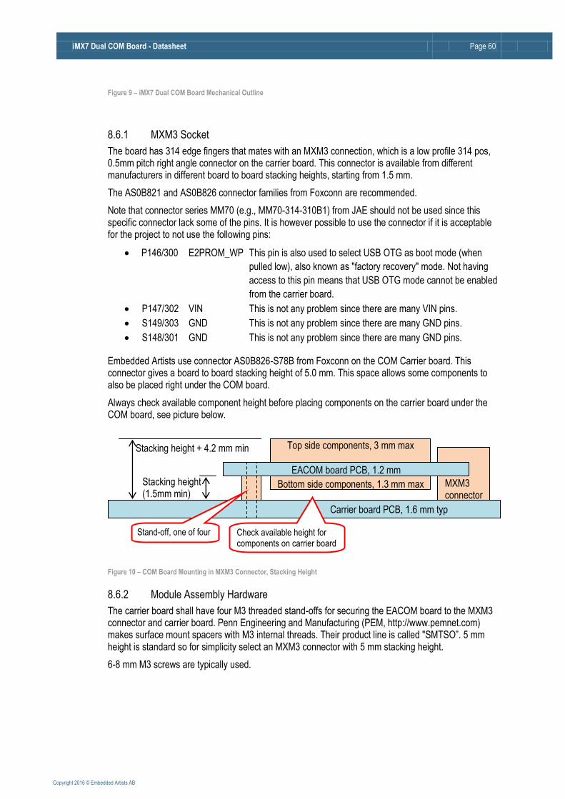
iMX7 Dual COM Board - Datasheet Page 60
Copyright 2016 © Embedded Artists AB
Figure 9 – iMX7 Dual COM Board Mechanical Outline
8.6.1 MXM3 Socket
The board has 314 edge fingers that mates with an MXM3 connection, which is a low profile 314 pos, 0.5mm pitch right angle connector on the carrier board. This connector is available from different manufacturers in different board to board stacking heights, starting from 1.5 mm.
The AS0B821 and AS0B826 connector families from Foxconn are recommended.
Note that connector series MM70 (e.g., MM70-314-310B1) from JAE should not be used since this specific connector lack some of the pins. It is however possible to use the connector if it is acceptable for the project to not use the following pins:
P146/300 E2PROM_WP This pin is also used to select USB OTG as boot mode (when
pulled low), also known as "factory recovery" mode. Not having
access to this pin means that USB OTG mode cannot be enabled
from the carrier board.
P147/302 VIN This is not any problem since there are many VIN pins.
S149/303 GND This is not any problem since there are many GND pins.
S148/301 GND This is not any problem since there are many GND pins.
Embedded Artists use connector AS0B826-S78B from Foxconn on the COM Carrier board. This connector gives a board to board stacking height of 5.0 mm. This space allows some components to also be placed right under the COM board.
Always check available component height before placing components on the carrier board under the COM board, see picture below.
Figure 10 – COM Board Mounting in MXM3 Connector, Stacking Height
8.6.2 Module Assembly Hardware
The carrier board shall have four M3 threaded stand-offs for securing the EACOM board to the MXM3 connector and carrier board. Penn Engineering and Manufacturing (PEM, http://www.pemnet.com) makes surface mount spacers with M3 internal threads. Their product line is called "SMTSO”. 5 mm height is standard so for simplicity select an MXM3 connector with 5 mm stacking height.
6-8 mm M3 screws are typically used.
Carrier board PCB, 1.6 mm typ
MXM3 connector
Bottom side components, 1.3 mm max
Top side components, 3 mm max
Stand-off, one of four
EACOM board PCB, 1.2 mm
Stacking height + 4.2 mm min
Stacking height (1.5mm min)
Check available height for components on carrier board

iMX7 Dual COM Board - Datasheet Page 61
Copyright 2016 © Embedded Artists AB
8.7 Environmental Specification
8.7.1 Operating Temperature
Ambient temperature (TA)
Parameter Min Max Unit
Operating temperature range: commercial temperature range industrial temperature range
0 -20
70[1]
85[1] °C °C
Storage temperature range -40 85 °C
Junction temperature i.MX 7Dual SoC, operating: comm. temp. range ind. temp. range.
0 -20
95 105
°C °C
[1] Depends on cooling solution.
8.7.2 Relative Humidity (RH)
Parameter Min Max Unit
Operating: 0°C ≤ TA ≤ 70°C, non-condensing (comm. temp. range) Operating: -20°C ≤ TA ≤ 85°C, non-condensing (ind. temp. range)
10 90 %
Non-operating/Storage: -40°C ≤ TA ≤ 85°C, non-condensing 5 90 %
8.8 Thermal Design Considerations
Heat dissipation from the i.MX 7Dual SoC depending on many operating conditions, like operating frequency, operating voltage, activity type, activity cycle duration and duty cycle. Dissipated heat is less than 1 Watt.
If external cooling is needed, or not, depends on dissipated heat and ambient temperature range. In most cases it is possible to operate the iMX7 Dual COM Board without external cooling, at least with ambient temperature up to +60° Celsius. Above this, care must be taken not to exceed max junction temperature of the i.MX 7Dual.
The i.MX 7Dual SoC and PMIC (PF3000) together implement DVFS (Dynamic Voltage and Frequency Scaling) and Thermal Throttling. This enables the system to continuously adjust operating frequency and voltage in response to changes in workload and temperature. In general this result in higher performance at lower average power consumption.
The .iMX 7Dual SoC has an integrated temperature sensor for monitoring the junction (i.e., die) temperature, which affect several factors:
A lower junction temperature, Tj, will result in longer SoC lifetime. See the following document for details: AN5334, i.MX7 Dual/Solo Product Lifetime Usage.
A lower die temperature will result in lower power consumption due to lower leakage current.
8.8.1 Thermal Parameters
The i.MX 7Dual SoC thermal parameters are listed in the table below.
Parameter Typical Unit
Thermal Resistance, CPU Junction to ambient (RθJA), natural convection 30.2 °C/W
Thermal Resistance, CPU Junction to package top (ψJT) 0.2 °C/W

iMX7 Dual COM Board - Datasheet Page 62
Copyright 2016 © Embedded Artists AB
8.9 Product Compliance
Visit Embedded Artists' website at http://www.embeddedartists.com/product_compliance for up to date information about product compliances such as CE, RoHS2, Conflict Minerals, REACH, etc.

iMX7 Dual COM Board - Datasheet Page 63
Copyright 2016 © Embedded Artists AB
9 Functional Verification and RMA There is a separate document that presents a number of functional tests that can be performed on the iMX7 Dual COM Board to verify correct operation on the different interfaces. Note that these tests must be performed on the carrier board that is supplied with the iMX7 Dual COM Developer's Kit and with a precompiled kernel from Embedded Artists.
The tests can also be done to troubleshoot a board that does not seem to operate properly. It is strongly advised to read through the list of tests and actions that can be done before contacting Embedded Artists. The different tests can help determine if there is a problem with the board, or not. For return policy, please read Embedded Artists’ General Terms and Conditions document (http://www.embeddedartists.com/sites/default/files/docs/General_Terms_and_Conditions.pdf).

iMX7 Dual COM Board - Datasheet Page 64
Copyright 2016 © Embedded Artists AB
10 Things to Note This chapter presents a number of issues and considerations that users must note.
10.1 Shared Pins and Multiplexing
The i.MX 7Dual SoC has multiple on-chip interfaces that are multiplexed on the external pins. It is not possible to use all interfaces simultaneously and some interface usage is prohibited by the iMX7 Dual COM on-board design. Check if the needed interfaces are available to allocation before starting a design. See chapter 4 for details.
10.2 Cannot Access Some Memory Cards
Some memory cards have a very high current consumption peak when turned on. This can cause problems accessing the memory cards because there voltage dip becomes too big.
As a solution, move the zero-ohm resistor in SJ8 to position 2-3 (instead of the default position: 1-2). This will power the memory card from the COM Carrier Board 3.3V supply instead of a supply from the iMX7 Dual COM board.
The picture below illustrates where SJ8 can be found on the bottom side of the COM Carrier Board.
Figure 11 – Location of SJ8 on COM Carrier Board
SJ8 Upper position: 1-2 Lower position: 2-3

iMX7 Dual COM Board - Datasheet Page 65
Copyright 2016 © Embedded Artists AB
10.3 Only Use EA Board Support Package (BSP)
The iMX7 Dual COM board use multiple on-board interfaces for the internal design, for example PMIC, eMMC and watchdog. Only use the BSP that is delivered from Embedded Artists. Do not change interface initialization and/or pin assignment for the on-board interfaces. Changing BSP settings can result in permanent board failure.
Note that Embedded Artists does not replace iMX7 Dual COM Boards that have been damaged because of improper interface initialization and/or improper pin assignment.
10.4 OTP Fuse Programming
The i.MX 7Dual SoC has on-chip OTP fuses that can be programmed, see NXP documents iMX 7Dual Datasheet and iMX 7Dual Reference Manual for details. Once programmed, there is no possibility to reprogram them.
iMX7 Dual COM Boards are delivered without any OTP fuse programming. It is completely up to the COM board user to decide if OTP fuses shall be programmed and in that case, which ones.
Note that Embedded Artists does not replace iMX7 Dual COM Boards because of wrong OTP programming. It’s the user’s responsibility to be absolutely certain before OTP programming and not to program the fuses by accident.
10.5 Write Protect on Parameter Storage E2PROM
The parameter storage E2PROM contains important system data like DDR memory initialization settings and Ethernet MAC addresses. The content should not be erased or overwritten. The E2PROM is write protected if signal E2PROM_WR (pin P146/300) is left unconnected, i.e. floating. This should always be the case.
Note that all carrier board design should include the possibility to ground this pin.
The signal E2PROM_WR has dual functions. By pulling the signal low, the i.MX 7 SoC will boot into USB OTG boot mode (also called 'serial download' or 'factory recovery' mode).
10.6 Integration - Contact Embedded Artists
It is strongly recommended to contact Embedded Artists at an early stage in your project. A wide range of support during evaluation and the design-in phase are offered, including but not limited to:
Developer's Kit to simplify evaluation
Custom Carrier board design, including 'ready-to-go' standard carrier boards
Display solutions
Mechanical solutions
Schematic review of customer carrier board designs
Driver and application development
The iMX7 Dual COM Board targets a wide range of applications, such as:
Portable systems
HMI/GUI solutions
Portable medical and health care
Connected vending machines
Point-of-Sale (POS) applications
Access control panels
Audio
IP phones
Smart appliances
eReaders

iMX7 Dual COM Board - Datasheet Page 66
Copyright 2016 © Embedded Artists AB
Wearables
Home energy management systems
Industrial automation
HVAC Building and Control Systems
Smart Grid and Smart Metering
Smart Toll Systems
Data acquisition
Communication gateway solutions
Connected real-time systems
...and much more
For more harsh use and environments, and where fail-safe operation, redundancy or other strict reliability or safety requirements exists, always contact Embedded Artists for a discussion about suitability.
There are application areas that the iMX7 Dual COM Board is not designed for (and such usage is strictly prohibited), for example:
Military equipment
Aerospace equipment
Control equipment for nuclear power industry
Medical equipment related to life support, etc.
Gasoline stations and oil refineries
If not before, it is essential to contact Embedded Artists before production begins. In order to ensure a reliable supply for you, as a customer, we need to know your production volume estimates and forecasts. Embedded Artists can typically provide smaller volumes of the iMX7 Dual COM Board directly from stock (for evaluation and prototyping), but larger volumes need to be planned.
The more information you can share with Embedded Artists about your plans, estimates and forecasts the higher the likelihood is that we can provide a reliable supply to you of the iMX7 Dual COM Board.
10.7 ESD Precaution when Handling iMX7 Dual COM Board
Please note that the iMX7 Dual COM Board come without any case/box and all components are exposed for finger touches – and therefore extra attention must be paid to ESD (electrostatic discharge) precaution, for example use of static-free workstation and grounding strap. Only qualified personnel shall handle the product.
Make it a habit always to first touch the mounting hole (which is grounded) for a few seconds with both hands before touching any other parts of the boards. That way, you will have the same potential as the board and therefore minimize the risk for ESD.
In general touch as little as possible on the boards in order to minimize the risk of ESD damage. The only reasons to touch the board are when mounting/unmounting it on a carrier board.
Note that Embedded Artists does not replace boards that have been damaged by ESD.
10.8 EMC / ESD
The iMX7 Dual COM Board has been developed according to the requirements of electromagnetic compatibility (EMC). Nevertheless depending on the target system, additional anti-interference measurement may still be necessary to adherence to the limits for the overall system.
The iMX7 Dual COM Board must be mounted on carrier board (typically an application specific board) and therefore EMC and ESD tests only makes sense on the complete solution.

iMX7 Dual COM Board - Datasheet Page 67
Copyright 2016 © Embedded Artists AB
No specific ESD protection has been implemented on the iMX7 Dual COM Board. ESD protection on board level is the same as what is specified in the i.MX 7Dual SoC datasheet. It is strongly advised to implement protection against electrostatic discharges (ESD) on the carrier board on all signals to and from the system. Such protection shall be arranged directly at the inputs/outputs of the system.

iMX7 Dual COM Board - Datasheet Page 68
Copyright 2016 © Embedded Artists AB
11 Custom Design This document specify the standard iMX7 Dual COM Board design. Embedded Artists offers many custom design services. Contact Embedded Artists for a discussion about different options.
Examples of custom design services are:
Different memory sizes on DDR3L SDRAM and eMMC Flash.
Different I/O voltage levels on all or parts of the pins.
Different mounting options, for example remove QSPI and/or Ethernet interface.
Different pinning on MXM3 edge pins, including but not limited to, SMARC compatible pinning.
Different board form factor, for example SODIMM-200, high-density connectors on bottom side or MXM3 compatible boards that are higher (>50 mm).
Different input supply voltage range, for example 5V input.
Single Board Computer solutions, where the core design of the iMX7 Dual COM Board is integrated together with selected interfaces.
Replace eMMC Flash with (unmanaged) MLC/SLC NAND Flash.
Changed internal pinning to make certain pins available.
Embedded Artists also offers a range of services to shorten development time and risk, such as:
Standard Carrier boards ready for integration
Custom Carrier board design
Display solutions
Mechanical solutions
iMX7 Dual COM Board - Datasheet Page 69
Copyright 2016 © Embedded Artists AB
12 Disclaimers Embedded Artists reserves the right to make changes to information published in this document, including, without limitation, specifications and product descriptions, at any time and without notice. This document supersedes and replaces all information supplied prior to the publication hereof.
Customer is responsible for the design and operation of their applications and products using Embedded Artists’ products, and Embedded Artists accepts no liability for any assistance with applications or customer product design. It is customer’s sole responsibility to determine whether the Embedded Artists’ product is suitable and fit for the customer’s applications and products planned, as well as for the planned application and use of customer’s third party customer(s). Customers should provide appropriate design and operating safeguards to minimize the risks associated with their applications and products. Customer is required to have expertise in electrical engineering and computer engineering for the installation and use of Embedded Artists’ products.
Embedded Artists does not accept any liability related to any default, damage, costs or problem which is based on any weakness or default in the customer’s applications or products, or the application or use by customer’s third party customer(s). Customer is responsible for doing all necessary testing for the customer’s applications and products using Embedded Artists’ products in order to avoid a default of the applications and the products or of the application or use by customer’s third party customer(s). Embedded Artists does not accept any liability in this respect.
Embedded Artists does not accept any liability for errata on individual components. Customer is responsible to make sure all errata published by the manufacturer of each component are taken note of. The manufacturer's advice should be followed.
Embedded Artists does not accept any liability and no warranty is given for any unexpected software behavior due to deficient components.
Customer is required to take note of manufacturer's specification of used components, for example PMIC and eMMC. Such specifications, if applicable, contains additional information that must be taken note of for the safe and reliable operation. These documents are stored on Embedded Artists' product support page.
All Embedded Artists’ products are sold pursuant to Embedded Artists’ terms and conditions of sale: http://www.embeddedartists.com/sites/default/files/docs/General_Terms_and_Conditions.pdf
No license, express or implied, by estoppel or otherwise, to any intellectual property rights is granted under this document. If any part of this document refers to any third party products or services it shall not be deemed a license grant by Embedded Artists for the use of such third party products or services, or any intellectual property contained therein or considered as a warranty covering the use in any manner whatsoever of such third party products or services or any intellectual property contained therein.
UNLESS OTHERWISE SET FORTH IN EMBEDDED ARTISTS’ TERMS AND CONDITIONS OF SALE EMBEDDED ARTISTS DISCLAIMS ANY EXPRESS OR IMPLIED WARRANTY WITH RESPECT TO THE USE AND/OR SALE OF EMBEDDED ARTISTS PRODUCTS INCLUDING WITHOUT LIMITATION IMPLIED WARRANTIES OF MERCHANTABILITY, FITNESS FOR A PARTICULAR PURPOSE (AND THEIR EQUIVALENTS UNDER THE LAWS OF ANY JURISDICTION), OR INFRINGEMENT OF ANY PATENT, COPYRIGHT OR OTHER INTELLECTUAL PROPERTY RIGHT.
UNLESS EXPRESSLY APPROVED IN WRITING BY THE CEO OF EMBEDDED ARTISTS, PRODUCTS ARE NOT RECOMMENDED, AUTHORIZED OR WARRANTED FOR USE IN MILITARY, AIR CRAFT, SPACE, NUCLEAR, LIFE SAVING, OR LIFE SUSTAINING APPLICATIONS, NOR IN PRODUCTS OR SYSTEMS WHERE FAILURE OR MALFUNCTION MAY RESULT IN PERSONAL INJURY, DEATH, OR SEVERE PROPERTY OR ENVIRONMENTAL DAMAGE.
Resale of Embedded Artists’ products with provisions different from the statements and/or technical features set forth in this document shall immediately void any warranty granted by Embedded Artists

iMX7 Dual COM Board - Datasheet Page 70
Copyright 2016 © Embedded Artists AB
for the Embedded Artists’ product or service described herein and shall not create or extend in any manner whatsoever, any liability of Embedded Artists.
This document as well as the item(s) described herein may be subject to export control regulations. Export might require a prior authorization from national authorities.
12.1 Definition of Document Status
Preliminary – The document is a draft version only. The content is still under internal review and subject to formal approval, which may result in modifications or additions. Embedded Artists does not give any representations or warranties as to the accuracy or completeness of information included herein and shall have no liability for the consequences of use of such information. The document is in this state until the product has passed Embedded Artists product qualification tests.
Approved – The information and data provided define the specification of the product as agreed between Embedded Artists and its customer, unless Embedded Artists and customer have explicitly agreed otherwise in writing.