Embed Size (px)
Citation preview

Rev.20190905
IMU (Inertial Measurement Unit)
M-G365PDData Sheet
Rev.20190905
NOTICE No part of this material may be reproduced or duplicated in any form or by any means without the written permission of Seiko Epson. Seiko Epson reserves the right to make changes to this material without notice. Seiko Epson does not assume any liability of any kind arising out of any inaccuracies contained in this material or due to its application or use in any product or circuit. This product is not designed to be used in the equipment that demands extremely high reliability and where its failure may threaten human life or property (for example, aerospace equipment, submarine repeater, nuclear power control equipment, life support equipment, medical equipment, transportation control equipment, etc.). Therefore, Seiko Epson Corporation will not be liable for any damages caused by the use of the product for those applications. Moreover, no license to any intellectual property rights is granted by implication or otherwise, and there is no representation or warranty that anything made in accordance with this material will be free from any patent or copyright infringement of a third party. When exporting the products or technology described in this material, you should comply with the applicable export control laws and regulations and follow the procedures required by such laws and regulations. You are requested not to use, to resell, to export and/or to otherwise dispose of the products (and any technical information furnished, if any) for the development and/or manufacture of weapon of mass destruction or for other military purposes.
All brands or product names mentioned herein are trademarks and/or registered trademarks of their respective companies.
©SEIKO EPSON CORPORATION 2019, All rights reserved.
M-G365PD Data Sheet SEIKO EPSON CORPORATION i Rev.20190905
Table of Contents
Table of Contents .............................................................................................................. i
1. General Description ................................................................................................... 1
1.1 Features ....................................................................................................................................... 1
1.2 Applications ................................................................................................................................ 1
1.3 Functional Block Diagram ......................................................................................................... 1
2. Product Specifications .............................................................................................. 2
2.1 Absolute Maximum Ratings ...................................................................................................... 2
2.2 Recommended Operating Condition ........................................................................................ 2
2.3 Characteristics and Electrical Specifications ......................................................................... 3
2.4 Timing Specifications ................................................................................................................ 5
2.5 Connector Pin Layout and Functions ...................................................................................... 7
3. Mechanical Dimensions ............................................................................................ 8
3.1 Outline Dimensions .................................................................................................................... 8
3.2 Connector Dimensions ............................................................................................................ 10
4. Typical Performance Characteristics ...................................................................... 11
5. Basic Operation ....................................................................................................... 13
5.1 Connection to Host .................................................................................................................. 13
5.2 Operation Mode ........................................................................................................................ 14
5.3 Functional Block Diagram ....................................................................................................... 15
5.4 Data Output Timing .................................................................................................................. 16
5.5 Data Ready Signal .................................................................................................................... 17
5.6 Sampling Counter..................................................................................................................... 17
5.7 GPIO ........................................................................................................................................... 17
5.8 Self Test ..................................................................................................................................... 17
5.9 External Trigger Input .............................................................................................................. 18
5.10 External Counter Reset Input .................................................................................................. 22
5.11 Checksum ................................................................................................................................. 23
5.12 Automatic Start (For UART Auto Mode Only) ....................................................................... 24
5.13 Filter ........................................................................................................................................... 24
5.14 Delta Angle/Delta Velocity Output .......................................................................................... 28
5.15 Attitude Output ......................................................................................................................... 30
5.16 Frame Alignment Correction ................................................................................................... 31
6. Digital Interface ......................................................................................................................... 32
6.1 SPI Interface .............................................................................................................................. 33 6.1.1 SPI Read Timing (Normal Mode) ........................................................................................ 34 6.1.2 SPI Write Timing (Normal Mode) ......................................................................................... 35 6.1.3 SPI Read Timing (Burst Mode) ............................................................................................ 36
6.2 UART Interface .......................................................................................................................... 37 6.2.1 UART Read Timing (Normal Mode) .................................................................................... 38 6.2.2 UART Read Timing (Burst Mode) ........................................................................................ 39 6.2.3 UART Write Timing .............................................................................................................. 39 6.2.4 UART Auto Mode Operation ................................................................................................ 40
6.3 Data Packet Format .................................................................................................................. 41
ii SEIKO EPSON CORPORATION M-G365PD Data Sheet
Rev.20190905
7. User Registers .......................................................................................................... 51
7.1 BURST Register (Window 0) ................................................................................................... 54
7.2 MODE_CTRL Register (Window 0) ......................................................................................... 54
7.3 DIAG_STAT Register (Window 0) ............................................................................................ 55
7.4 FLAG(ND/EA) Register (Window 0) ........................................................................................ 56
7.5 GPIO Register (Window 0) ....................................................................................................... 57
7.6 COUNT Register (Window 0) ................................................................................................... 57
7.7 RANGE OVER Register (Window 0) ....................................................................................... 58
7.8 TEMP Register (Window 0) ...................................................................................................... 58
7.9 GYRO Register (Window 0) ..................................................................................................... 59
7.10 ACCL Register (Window 0) ...................................................................................................... 59
7.11 DELTA_ANGLE Register (Window 0)...................................................................................... 60
7.12 DELTA_VELOCITY Register (Window 0) ................................................................................ 60
7.13 ATTI Register (Window 0) ........................................................................................................ 61
7.14 SIG_CTRL Register (Window 1) .............................................................................................. 61
7.15 MSC_CTRL Register (Window 1) ............................................................................................ 62
7.16 SMPL_CTRL Register (Window 1) .......................................................................................... 63
7.17 FILTER_CTRL Register (Window 1) ........................................................................................ 66
7.18 UART_CTRL Register (Window 1) .......................................................................................... 67
7.19 GLOB_CMD Register (Window 1) ........................................................................................... 68
7.20 BURST_CTRL1 Register (Window 1) ...................................................................................... 69
7.21 BURST_CTRL2 Register (Window 1) ...................................................................................... 70
7.22 POL_CTRL Register (Window 1) ............................................................................................. 71
7.23 DLT_CTRL Register (Window 1) ............................................................................................. 72
7.24 ATTI_CTRL Register (Window 1) ............................................................................................ 74
7.25 GLOB_CMD2 Register (Window 1) ......................................................................................... 76
7.26 EXT_SYNC_CTRL Register (Window 1) ................................................................................. 76
7.27 R_MATRIX Register (Window 1).............................................................................................. 77
7.28 PROD_ID Register (Window 1) ................................................................................................ 78
7.29 VERSION Register (Window 1)................................................................................................ 78
7.30 SERIAL_NUM Register (Window 1) ........................................................................................ 78
7.31 WIN_CTRL Register (Window 0,1) .......................................................................................... 79
8. Sample Program Sequence ..................................................................................... 80
8.1 SPI Sequence ............................................................................................................................ 80 8.1.1 Power-on sequence (SPI) ................................................................................................... 80 8.1.2 Register read and write (SPI) .............................................................................................. 80 8.1.3 Sampling data (SPI) ............................................................................................................ 80 8.1.4 Selftest (SPI) ........................................................................................................................ 83 8.1.5 Software reset (SPI) ............................................................................................................ 84 8.1.6 Flash test (SPI) .................................................................................................................... 84 8.1.7 Flash backup (SPI) .............................................................................................................. 84 8.1.8 Filter setting (SPI) ................................................................................................................ 85 8.1.9 Attitude output (SPI) ............................................................................................................ 85
8.2 UART Sequence ........................................................................................................................ 87 8.2.1 Power-on sequence (UART) ............................................................................................... 87 8.2.2 Register read and write (UART) .......................................................................................... 87 8.2.3 Sampling data (UART) ........................................................................................................ 87 8.2.4 Selftest (UART) .................................................................................................................... 90
M-G365PD Data Sheet SEIKO EPSON CORPORATION iii Rev.20190905
8.2.5 Software reset (UART) ........................................................................................................ 90 8.2.6 Flash test (UART) ................................................................................................................ 90 8.2.7 Flash backup (UART) .......................................................................................................... 91 8.2.8 Filter setting (UART) ............................................................................................................ 91 8.2.9 Auto Start (UART only) ........................................................................................................ 91 8.2.10 Attitude output (UART) ........................................................................................................ 92
9. Handling Notes ......................................................................................................... 94
9.1 Cautions for use ....................................................................................................................... 94
9.2 Cautions for storage ................................................................................................................ 94
9.3 Other cautions .......................................................................................................................... 95
9.4 Limited warranty ....................................................................................................................... 95
10. Part Number / Ordering Info. ................................................................................... 95
11. Evaluation Tools ...................................................................................................... 95
Revision History ............................................................................................................. 96
M-G365PD Data Sheet SEIKO EPSON CORPORATION 1 Rev.20190704
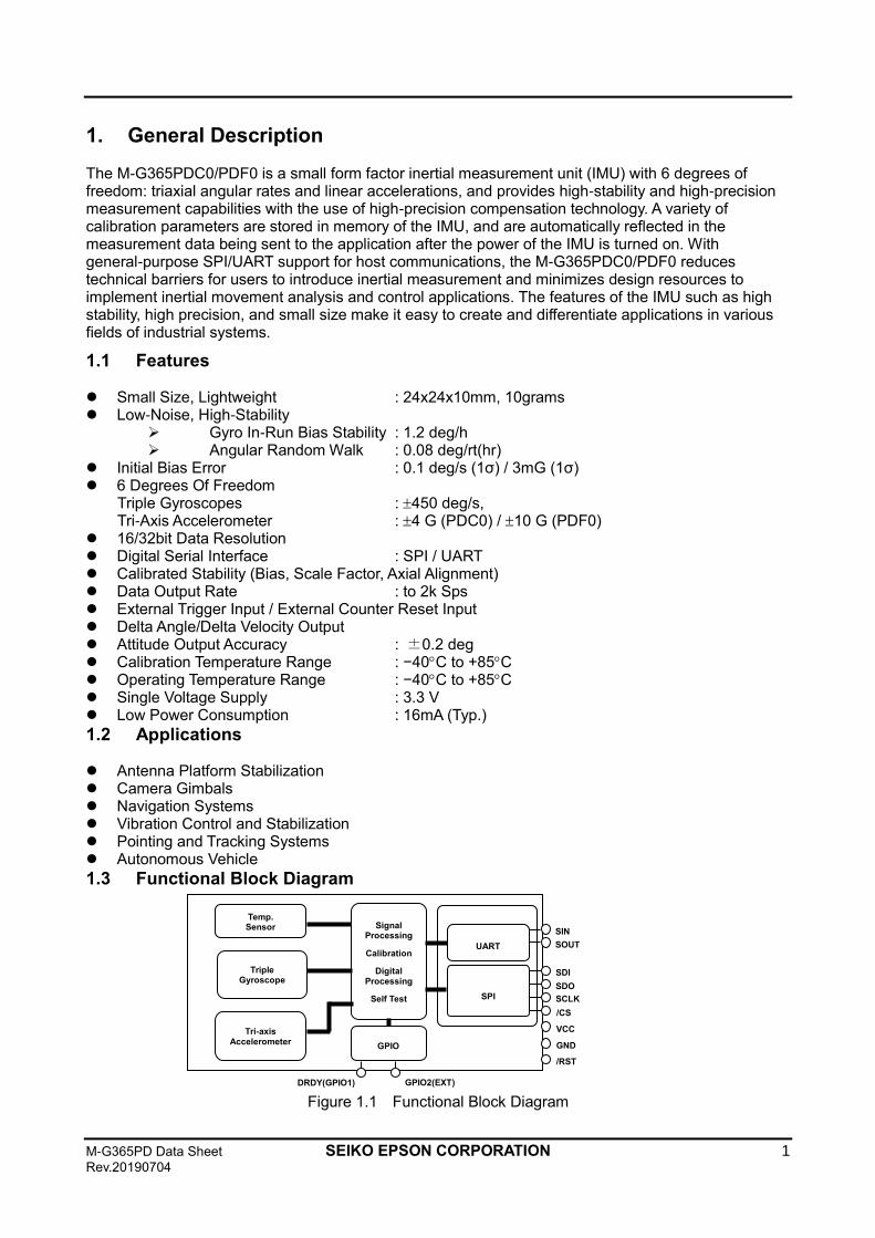
1. General Description
The M-G365PDC0/PDF0 is a small form factor inertial measurement unit (IMU) with 6 degrees of freedom: triaxial angular rates and linear accelerations, and provides high-stability and high-precision measurement capabilities with the use of high-precision compensation technology. A variety of calibration parameters are stored in memory of the IMU, and are automatically reflected in the measurement data being sent to the application after the power of the IMU is turned on. With general-purpose SPI/UART support for host communications, the M-G365PDC0/PDF0 reduces technical barriers for users to introduce inertial measurement and minimizes design resources to implement inertial movement analysis and control applications. The features of the IMU such as high stability, high precision, and small size make it easy to create and differentiate applications in various fields of industrial systems.
1.1 Features
⚫ Small Size, Lightweight : 24x24x10mm, 10grams ⚫ Low-Noise, High-Stability
➢ Gyro In-Run Bias Stability : 1.2 deg/h ➢ Angular Random Walk : 0.08 deg/rt(hr)
⚫ Initial Bias Error : 0.1 deg/s (1σ) / 3mG (1σ) ⚫ 6 Degrees Of Freedom Triple Gyroscopes : 450 deg/s, Tri-Axis Accelerometer : 4 G (PDC0) / 10 G (PDF0) ⚫ 16/32bit Data Resolution ⚫ Digital Serial Interface : SPI / UART ⚫ Calibrated Stability (Bias, Scale Factor, Axial Alignment) ⚫ Data Output Rate : to 2k Sps ⚫ External Trigger Input / External Counter Reset Input ⚫ Delta Angle/Delta Velocity Output ⚫ Attitude Output Accuracy : ±0.2 deg ⚫ Calibration Temperature Range : −40C to +85C ⚫ Operating Temperature Range : −40C to +85C ⚫ Single Voltage Supply : 3.3 V ⚫ Low Power Consumption : 16mA (Typ.)
1.2 Applications
⚫ Antenna Platform Stabilization ⚫ Camera Gimbals ⚫ Navigation Systems ⚫ Vibration Control and Stabilization ⚫ Pointing and Tracking Systems ⚫ Autonomous Vehicle
1.3 Functional Block Diagram
Figure 1.1 Functional Block Diagram
Temp. Sensor
Triple Gyroscope
Tri-axis Accelerometer
Signal Processing
Calibration
Digital Processing
Self Test
GPIO
SDI
SDO
SCLK
/CS
SIN
SOUT
DRDY(GPIO1)
GND
SPI
UART
/RST
VCC
GPIO2(EXT)
2 SEIKO EPSON CORPORATION M-G365PD Data Sheet
Rev.20190905
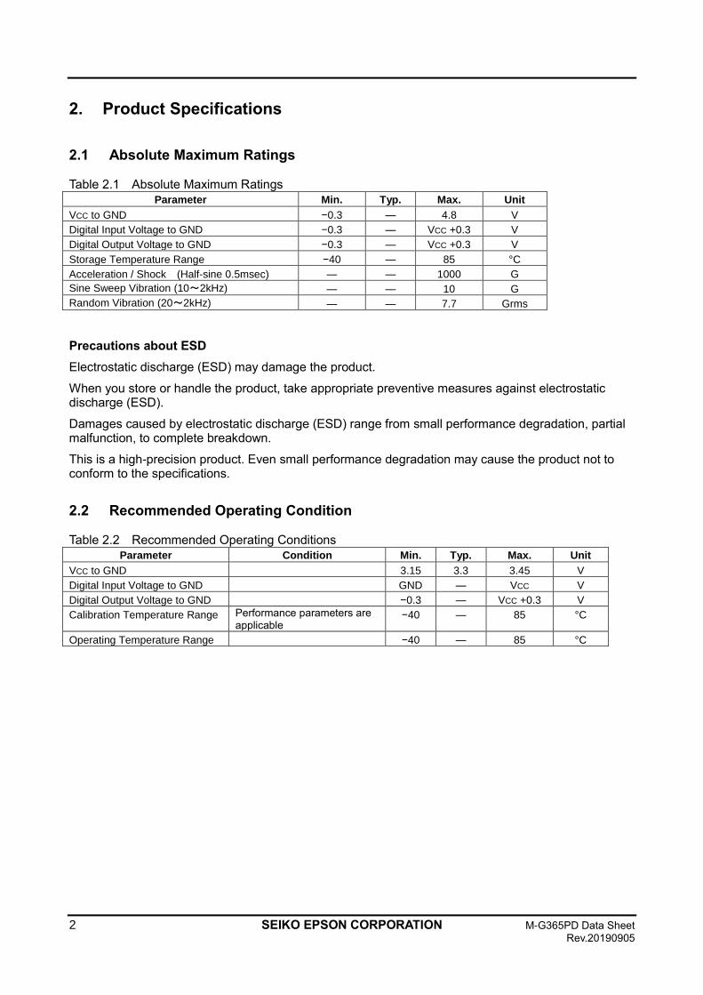
2. Product Specifications
2.1 Absolute Maximum Ratings
Table 2.1 Absolute Maximum Ratings
Parameter Min. Typ. Max. Unit
VCC to GND −0.3 - 4.8 V
Digital Input Voltage to GND −0.3 - VCC +0.3 V
Digital Output Voltage to GND −0.3 - VCC +0.3 V
Storage Temperature Range −40 - 85 °C
Acceleration / Shock (Half-sine 0.5msec) - - 1000 G
Sine Sweep Vibration (10~2kHz) - - 10 G
Random Vibration (20~2kHz) - - 7.7 Grms
Precautions about ESD
Electrostatic discharge (ESD) may damage the product.
When you store or handle the product, take appropriate preventive measures against electrostatic discharge (ESD).
Damages caused by electrostatic discharge (ESD) range from small performance degradation, partial malfunction, to complete breakdown.
This is a high-precision product. Even small performance degradation may cause the product not to conform to the specifications.
2.2 Recommended Operating Condition
Table 2.2 Recommended Operating Conditions
Parameter Condition Min. Typ. Max. Unit
VCC to GND 3.15 3.3 3.45 V
Digital Input Voltage to GND GND - VCC V
Digital Output Voltage to GND −0.3 - VCC +0.3 V
Calibration Temperature Range Performance parameters are applicable
−40 - 85 °C
Operating Temperature Range −40 - 85 °C
M-G365PD Data Sheet SEIKO EPSON CORPORATION 3 Rev.20190704
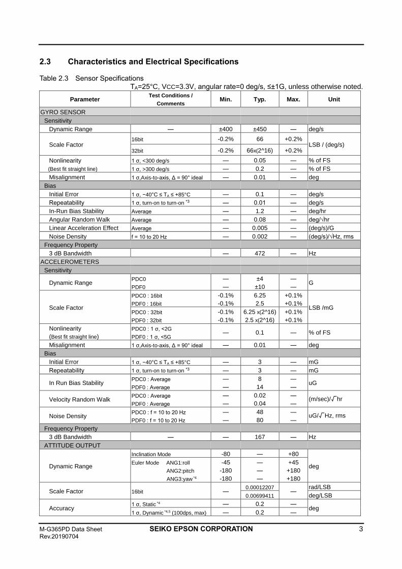
2.3 Characteristics and Electrical Specifications
Table 2.3 Sensor Specifications TA=25°C, VCC=3.3V, angular rate=0 deg/s, ≤±1G, unless otherwise noted.
Parameter Test Conditions /
Comments Min. Typ. Max. Unit
GYRO SENSOR
Sensitivity
Dynamic Range - ±400 ±450 - deg/s
Scale Factor 16bit -0.2% 66 +0.2%
LSB / (deg/s) 32bit -0.2% 66x(2^16) +0.2%
Nonlinearity
(Best fit straight line)
1 σ, <300 deg/s - 0.05 - % of FS
1 σ, >300 deg/s - 0.2 - % of FS
Misalignment 1 σ,Axis-to-axis, Δ = 90° ideal - 0.01 - deg
Bias
Initial Error 1 σ, −40°C ≤ TA ≤ +85°C - 0.1 - deg/s
Repeatability 1 σ, turn-on to turn-on *3 - 0.01 - deg/s
In-Run Bias Stability Average - 1.2 - deg/hr
Angular Random Walk Average - 0.08 - deg/√hr
Linear Acceleration Effect Average - 0.005 - (deg/s)/G
Noise Density f = 10 to 20 Hz - 0.002 - (deg/s)/√Hz, rms
Frequency Property
3 dB Bandwidth - 472 - Hz
ACCELEROMETERS
Sensitivity
Dynamic Range PDC0
PDF0
-
-
±4
±10
-
- G
Scale Factor
PDC0 : 16bit
PDF0 : 16bit
-0.1%
-0.1%
6.25
2.5
+0.1%
+0.1% LSB /mG
PDC0 : 32bit
PDF0 : 32bit
-0.1%
-0.1%
6.25 x(2^16)
2.5 x(2^16)
+0.1%
+0.1%
Nonlinearity
(Best fit straight line)
PDC0 : 1 σ, <2G
PDF0 : 1 σ, <5G - 0.1 - % of FS
Misalignment 1 σ,Axis-to-axis, Δ = 90° ideal - 0.01 - deg
Bias
Initial Error 1 σ, −40°C ≤ TA ≤ +85°C - 3 - mG
Repeatability 1 σ, turn-on to turn-on *3 - 3 - mG
In Run Bias Stability PDC0 : Average
PDF0 : Average
-
-
8
14
-
- uG
Velocity Random Walk PDC0 : Average
PDF0 : Average
-
-
0.02
0.04
-
- (m/sec)/√hr
Noise Density PDC0 : f = 10 to 20 Hz
PDF0 : f = 10 to 20 Hz
-
-
48
80
-
- uG/√Hz, rms
Frequency Property
3 dB Bandwidth - - 167 - Hz
ATTITUDE OUTPUT
Dynamic Range
Inclination Mode -80 - +80
deg Euler Mode ANG1:roll
ANG2:pitch
ANG3:yaw *4
-45
-180
-180
-
-
-
+45
+180
+180
Scale Factor 16bit - 0.00012207
- rad/LSB
0.00699411 deg/LSB
Accuracy 1 σ, Static *4 - 0.2 -
deg 1 σ, Dynamic *4,5 (100dps, max) - 0.2 -
4 SEIKO EPSON CORPORATION M-G365PD Data Sheet
Rev.20190905
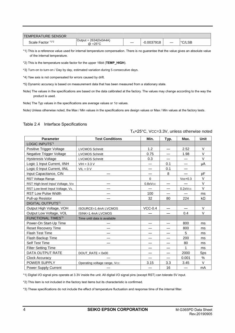
TEMPERATURE SENSOR
Scale Factor *1*2 Output = 2634(0x0A4A)
@ +25°C - -0.0037918 - °C/LSB
*1) This is a reference value used for internal temperature compensation. There is no guarantee that the value gives an absolute value
of the internal temperature.
*2) This is the temperature scale factor for the upper 16bit (TEMP_HIGH).
*3) Turn-on to turn-on / Day by day, estimated variation during 5 consecutive days.
*4) Yaw axis is not compensated for errors caused by drift.
*5) Dynamic accuracy is based on measurement data that has been measured from a stationary state.
Note) The values in the specifications are based on the data calibrated at the factory. The values may change according to the way the
product is used.
Note) The Typ values in the specifications are average values or 1σ values.
Note) Unless otherwise noted, the Max / Min values in the specifications are design values or Max / Min values at the factory tests.
Table 2.4 Interface Specifications
TA=25°C, VCC=3.3V, unless otherwise noted
Parameter Test Conditions Min. Typ. Max. Unit
LOGIC INPUTS*1
Positive Trigger Voltage LVCMOS Schmitt 1.2 - 2.52 V
Negative Trigger Voltage LVCMOS Schmitt 0.75 - 1.98 V
Hysteresis Voltage LVCMOS Schmitt 0.3 - - V
Logic 1 Input Current, IINH VIH = 3.3 V - 0.1 - μA
Logic 0 Input Current, IINL VIL = 0 V - 0.1 -
Input Capacitance, CIN - - 8 - pF
RST Voltage Range 0 Vcc+0.3 V
RST High-level Input Voltage, VIH - 0.8xVCC - - V
RST Low-level Input Voltage, VIL - - - 0.2xVCC V
RST Low Pulse Width - 100 - - ms
Pull-up Resistor - 32 80 224 kΩ
DIGITAL OUTPUTS*1
Output High Voltage, VOH ISOURCE=1.4mA LVCMOS VCC-0.4 - - V
Output Low Voltage, VOL ISINK=1.4mA LVCMOS - - 0.4 V
FUNCTIONAL TIMES*3 Time until data is available
Power-On Start-Up Time - - - 800 ms
Reset Recovery Time - - - 800 ms
Flash Test Time - - - 5 ms
Flash Backup Time - - - 200 ms
Self Test Time - - - 80 ms
Filter Setting Time - - 1 ms
DATA OUTPUT RATE DOUT_RATE = 0x00 - - 2000 Sps
Clock Accuracy - - - 0.001 %
POWER SUPPLY Operating voltage range, VCC 3.15 3.3 3.45 V
Power Supply Current - - 16 - mA
*1) Digital I/O signal pins operate at 3.3V inside the unit. All digital I/O signal pins (except RST) can tolerate 5V input.
*2) This item is not included in the factory test items but its characteristic is confirmed.
*3) These specifications do not include the effect of temperature fluctuation and response time of the internal filter.
M-G365PD Data Sheet SEIKO EPSON CORPORATION 5 Rev.20190704
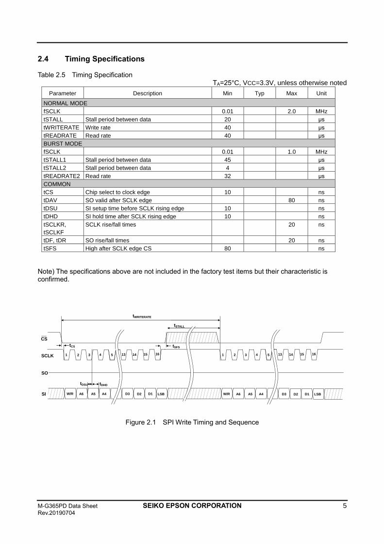
2.4 Timing Specifications
Table 2.5 Timing Specification TA=25°C, VCC=3.3V, unless otherwise noted
Parameter Description Min Typ Max Unit
NORMAL MODE
fSCLK 0.01 2.0 MHz
tSTALL Stall period between data 20 μs
tWRITERATE Write rate 40 μs
tREADRATE Read rate 40 μs
BURST MODE
fSCLK 0.01 1.0 MHz
tSTALL1 Stall period between data 45 μs
tSTALL2 Stall period between data 4 μs
tREADRATE2 Read rate 32 μs
COMMON
tCS Chip select to clock edge 10 ns
tDAV SO valid after SCLK edge 80 ns
tDSU SI setup time before SCLK rising edge 10 ns
tDHD SI hold time after SCLK rising edge 10 ns
tSCLKR,
tSCLKF
SCLK rise/fall times 20 ns
tDF, tDR SO rise/fall times 20 ns
tSFS High after SCLK edge CS 80 ns
Note) The specifications above are not included in the factory test items but their characteristic is confirmed.
CS
SCLK
SO
SI W/R
1 2 16 15 3
LSB A6 D1
4 5
D2 D3 A5 A4
14 13
W/R
1 2 16 15 3
LSB A6 D1
4 5
D2 D3 A5 A4
14 13
tDHD tDSU
tCS tSFS
tSTALL
tWRITERATE
Figure 2.1 SPI Write Timing and Sequence
6 SEIKO EPSON CORPORATION M-G365PD Data Sheet
Rev.20190905
CS
SCLK
SO
SI
MSB
W/R
LSB DB14 DB2
1 2 16 15 3
LSB A6 D1
4 5
D2 D3 A5 A4
DB13 DB12 DB3 DB1
14 13
MSB
W/R
LSB DB14 DB2
1 2 16 15 3
LSB A6 D1
4 5
D2 D3 A5 A4
DB13 DB12 DB3 DB1
14 13
tDHD tDSU
tDAV
tCS tSFS
tSTALL
tREADRATE
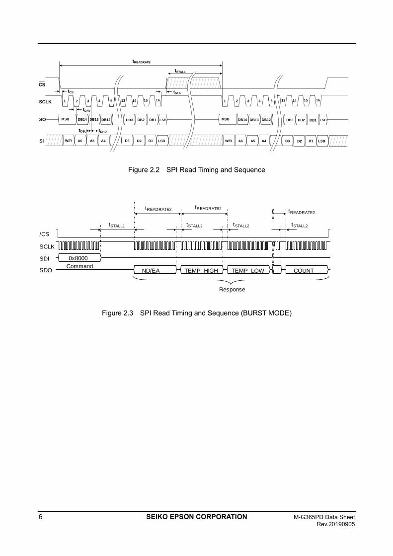
Figure 2.2 SPI Read Timing and Sequence
Figure 2.3 SPI Read Timing and Sequence (BURST MODE)
/CS
tSTALL1 tSTALL2
tREADRATE2
Response
SCLK
SDO
SDI
CommandND/EA TEMP_HIGH TEMP_LOW COUNT
tSTALL2tSTALL2
tREADRATE2tREADRATE2
0x8000
M-G365PD Data Sheet SEIKO EPSON CORPORATION 7 Rev.20190704
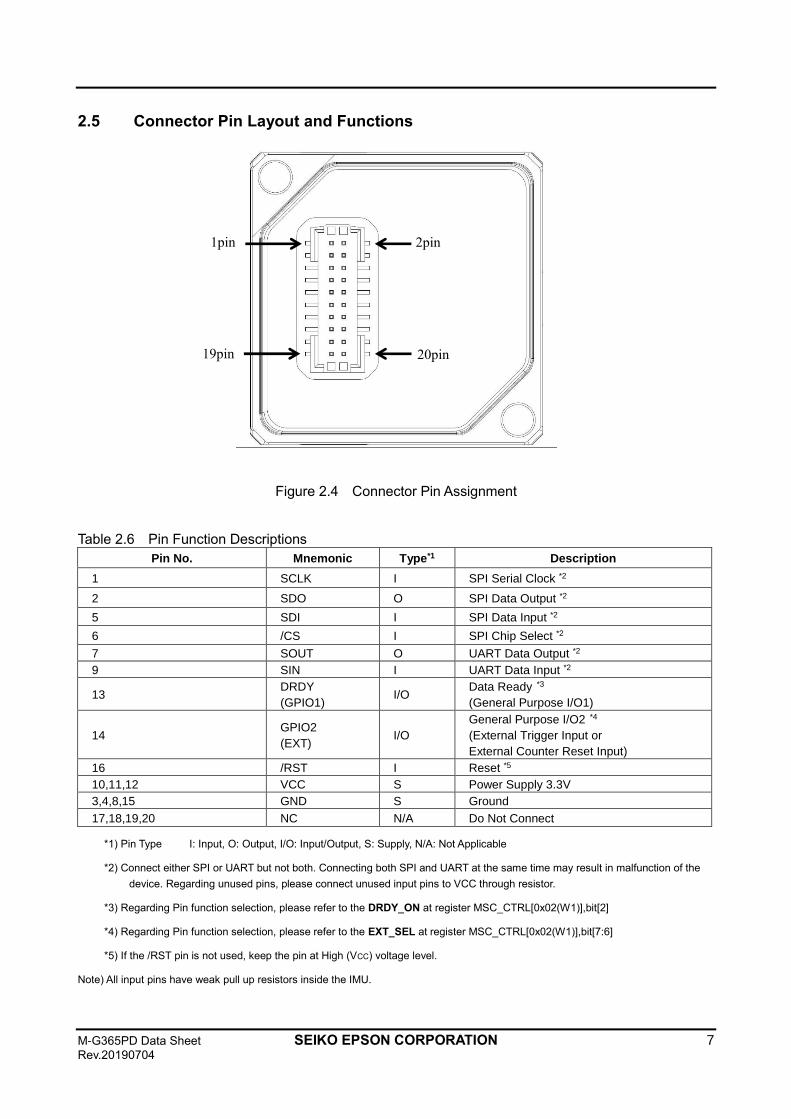
2.5 Connector Pin Layout and Functions
Figure 2.4 Connector Pin Assignment
Table 2.6 Pin Function Descriptions
Pin No. Mnemonic Type*1 Description
1 SCLK I SPI Serial Clock *2
2 SDO O SPI Data Output *2
5 SDI I SPI Data Input *2
6 /CS I SPI Chip Select *2
7 SOUT O UART Data Output *2
9 SIN I UART Data Input *2
13 DRDY
(GPIO1) I/O
Data Ready *3
(General Purpose I/O1)
14 GPIO2
(EXT) I/O
General Purpose I/O2 *4
(External Trigger Input or
External Counter Reset Input)
16 /RST I Reset *5
10,11,12 VCC S Power Supply 3.3V
3,4,8,15 GND S Ground
17,18,19,20 NC N/A Do Not Connect
*1) Pin Type I: Input, O: Output, I/O: Input/Output, S: Supply, N/A: Not Applicable
*2) Connect either SPI or UART but not both. Connecting both SPI and UART at the same time may result in malfunction of the
device. Regarding unused pins, please connect unused input pins to VCC through resistor.
*3) Regarding Pin function selection, please refer to the DRDY_ON at register MSC_CTRL[0x02(W1)],bit[2]
*4) Regarding Pin function selection, please refer to the EXT_SEL at register MSC_CTRL[0x02(W1)],bit[7:6]
*5) If the /RST pin is not used, keep the pin at High (VCC) voltage level.
Note) All input pins have weak pull up resistors inside the IMU.
1pin 2pin
19pin 20pin
8 SEIKO EPSON CORPORATION M-G365PD Data Sheet
Rev.20190905
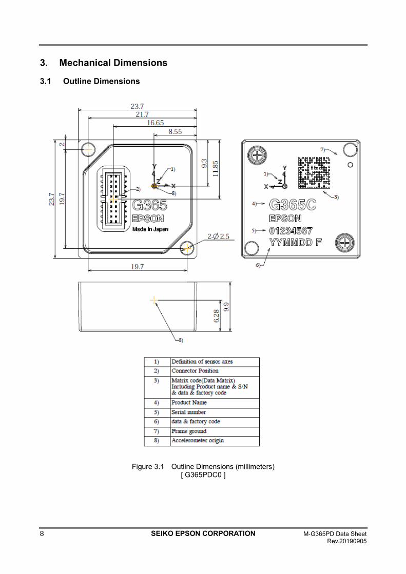
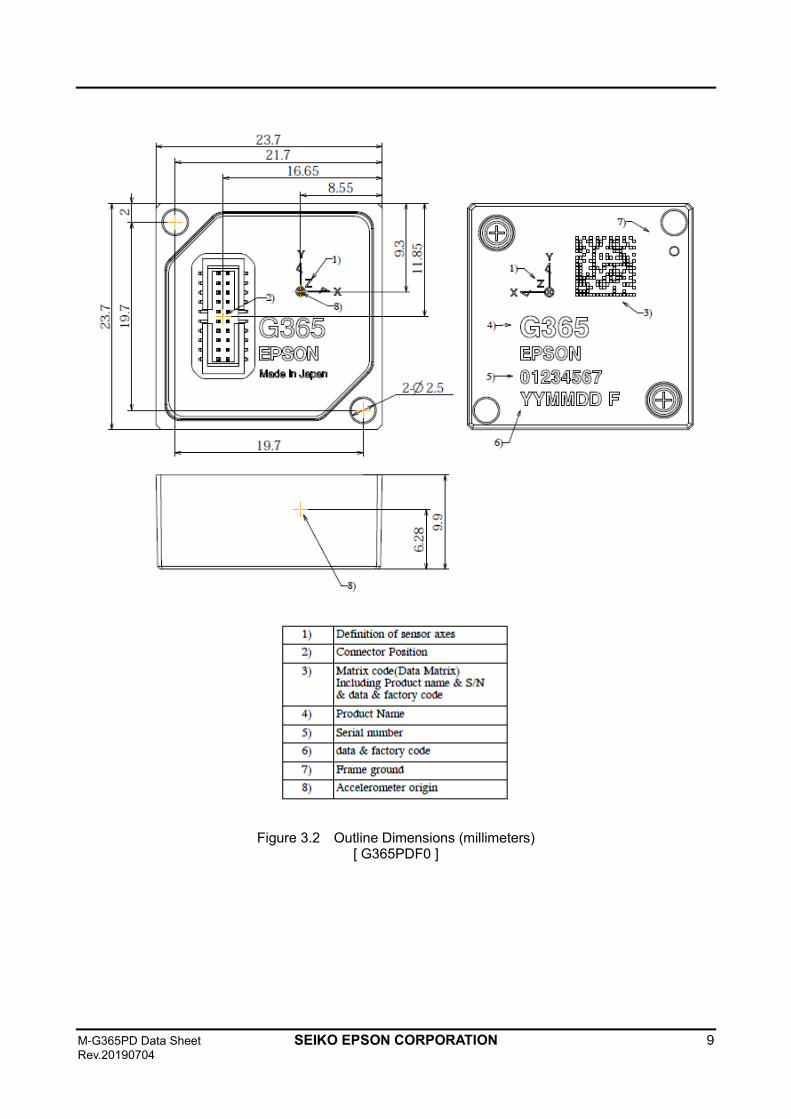
3. Mechanical Dimensions
3.1 Outline Dimensions
Figure 3.1 Outline Dimensions (millimeters) [ G365PDC0 ]
M-G365PD Data Sheet SEIKO EPSON CORPORATION 9 Rev.20190704
Figure 3.2 Outline Dimensions (millimeters) [ G365PDF0 ]
10 SEIKO EPSON CORPORATION M-G365PD Data Sheet
Rev.20190905
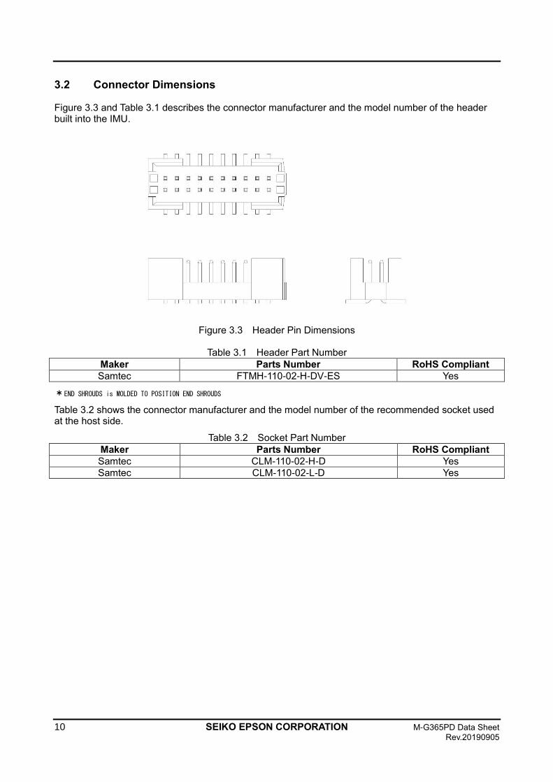
3.2 Connector Dimensions
Figure 3.3 and Table 3.1 describes the connector manufacturer and the model number of the header built into the IMU.
Figure 3.3 Header Pin Dimensions
Table 3.1 Header Part Number
Maker Parts Number RoHS Compliant
Samtec FTMH-110-02-H-DV-ES Yes
*END SHROUDS is MOLDED TO POSITION END SHROUDS
Table 3.2 shows the connector manufacturer and the model number of the recommended socket used at the host side.
Table 3.2 Socket Part Number
Maker Parts Number RoHS Compliant
Samtec CLM-110-02-H-D Yes
Samtec CLM-110-02-L-D Yes
M-G365PD Data Sheet SEIKO EPSON CORPORATION 11 Rev.20190704
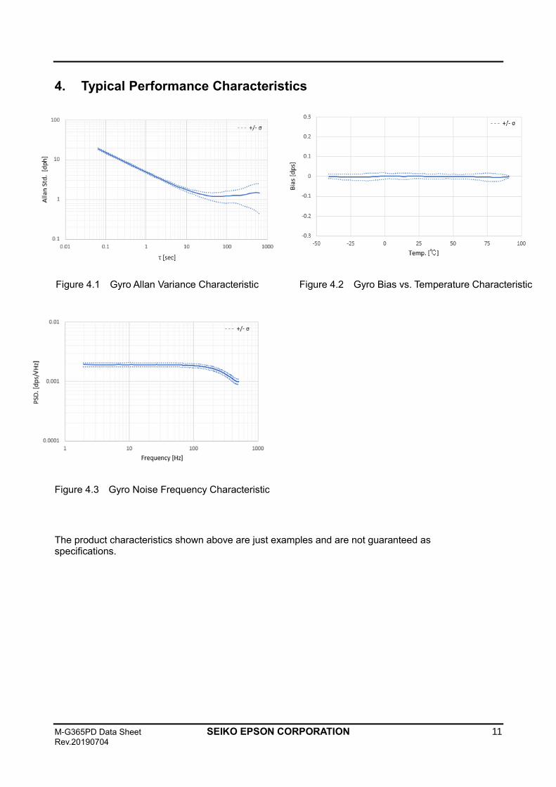
4. Typical Performance Characteristics
Figure 4.3 Gyro Noise Frequency Characteristic
The product characteristics shown above are just examples and are not guaranteed as specifications.
Figure 4.1 Gyro Allan Variance Characteristic
Figure 4.2 Gyro Bias vs. Temperature Characteristic
12 SEIKO EPSON CORPORATION M-G365PD Data Sheet
Rev.20190905
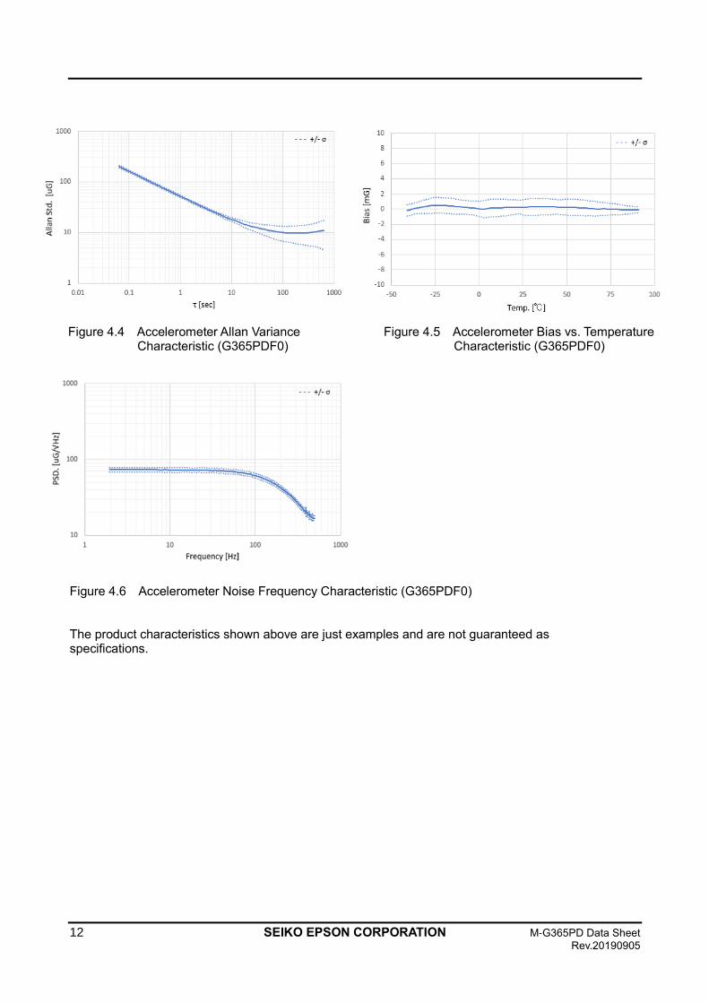
Figure 4.6 Accelerometer Noise Frequency Characteristic (G365PDF0)
The product characteristics shown above are just examples and are not guaranteed as specifications.
Figure 4.4 Accelerometer Allan Variance Characteristic (G365PDF0)
Figure 4.5 Accelerometer Bias vs. Temperature Characteristic (G365PDF0)
M-G365PD Data Sheet SEIKO EPSON CORPORATION 13 Rev.20190704
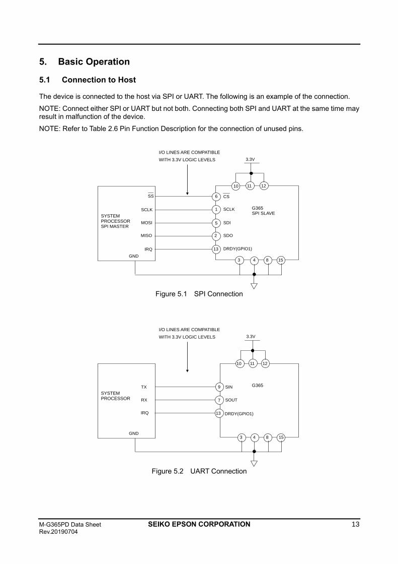
5. Basic Operation
5.1 Connection to Host
The device is connected to the host via SPI or UART. The following is an example of the connection.
NOTE: Connect either SPI or UART but not both. Connecting both SPI and UART at the same time may result in malfunction of the device.
NOTE: Refer to Table 2.6 Pin Function Description for the connection of unused pins.
SS
SCLK
MOSI
MISO
IRQ
SYSTEM PROCESSOR SPI MASTER
I/O LINES ARE COMPATIBLE
WITH 3.3V LOGIC LEVELS
6
1
5
2
13
10 11
8
G365 SPI SLAVE
CS
SCLK
SDI
SDO
DRDY(GPIO1)
3.3V
15 4 GND
3
12
Figure 5.1 SPI Connection
TX
RX
IRQ
SYSTEM PROCESSOR
I/O LINES ARE COMPATIBLE
WITH 3.3V LOGIC LEVELS
9
7
13
10 12
3 8
G365 SIN
SOUT
DRDY(GPIO1)
3.3V
15 4 GND
11
Figure 5.2 UART Connection
14 SEIKO EPSON CORPORATION M-G365PD Data Sheet
Rev.20190905
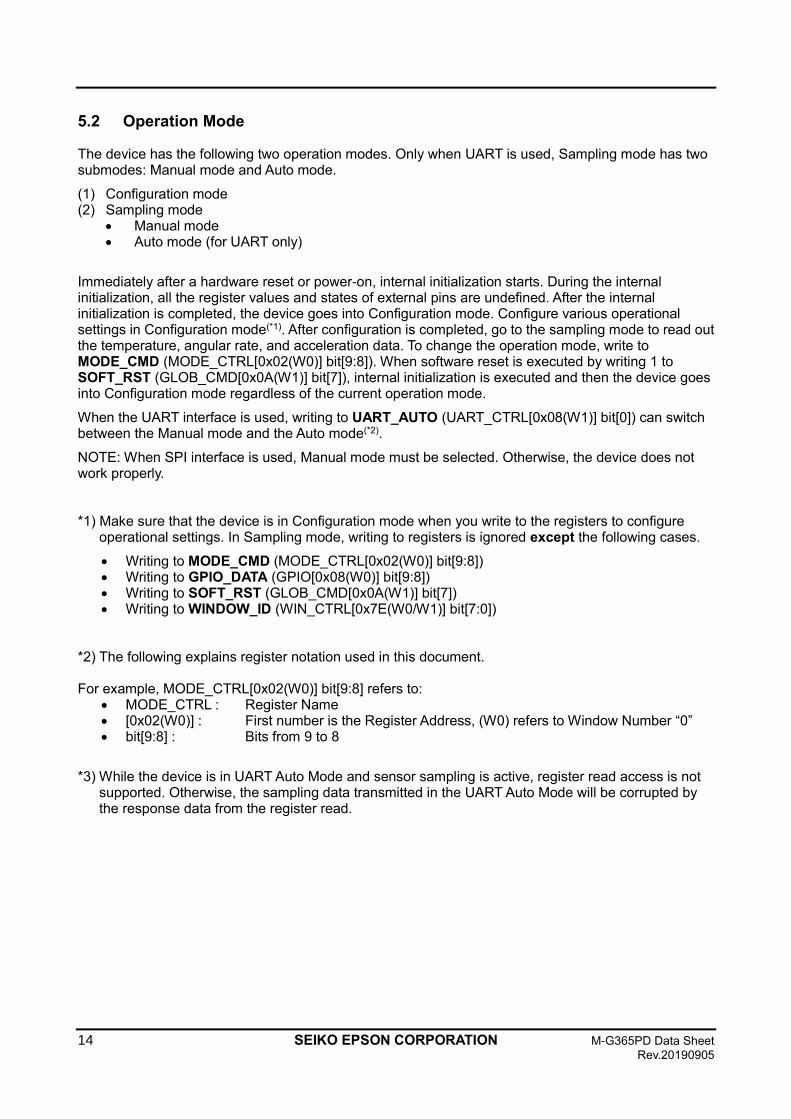
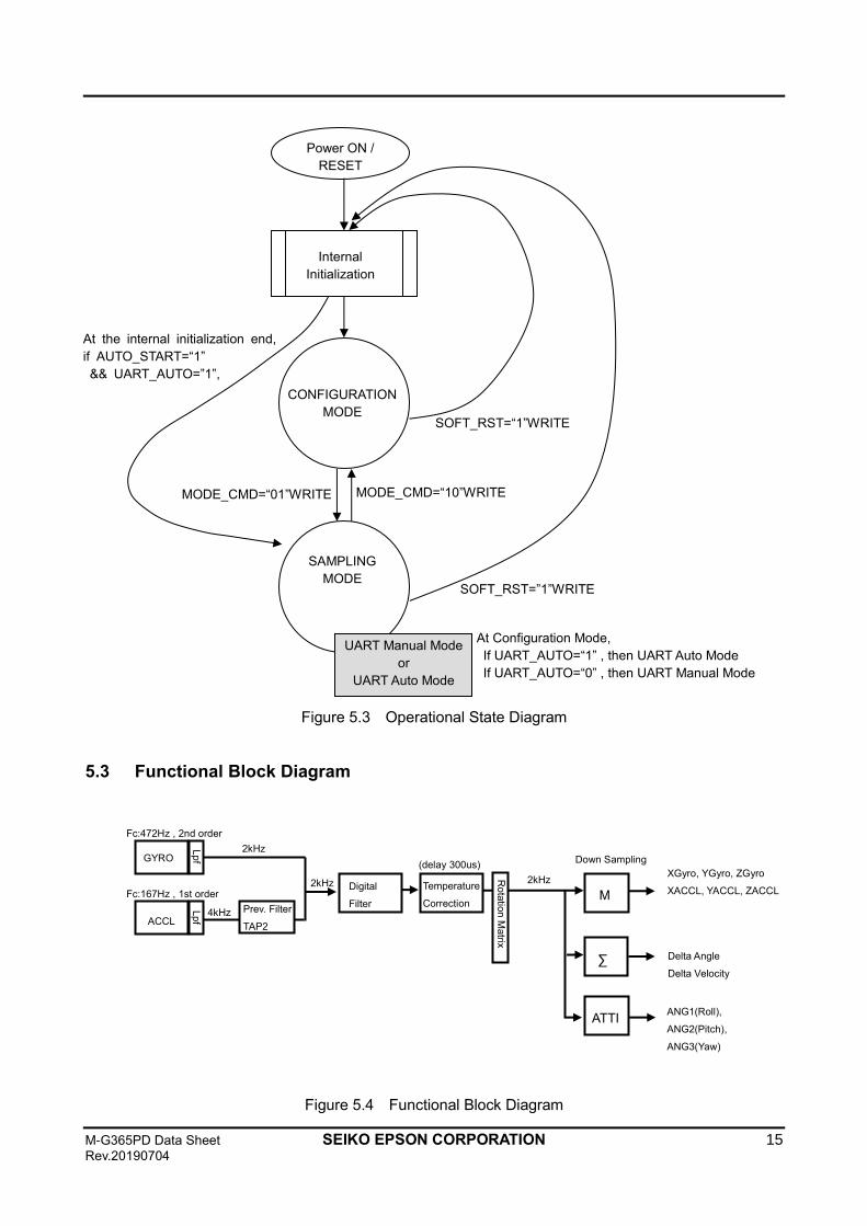
5.2 Operation Mode
The device has the following two operation modes. Only when UART is used, Sampling mode has two submodes: Manual mode and Auto mode.
(1) Configuration mode (2) Sampling mode
• Manual mode • Auto mode (for UART only)
Immediately after a hardware reset or power-on, internal initialization starts. During the internal initialization, all the register values and states of external pins are undefined. After the internal initialization is completed, the device goes into Configuration mode. Configure various operational settings in Configuration mode(*1). After configuration is completed, go to the sampling mode to read out the temperature, angular rate, and acceleration data. To change the operation mode, write to MODE_CMD (MODE_CTRL[0x02(W0)] bit[9:8]). When software reset is executed by writing 1 to SOFT_RST (GLOB_CMD[0x0A(W1)] bit[7]), internal initialization is executed and then the device goes into Configuration mode regardless of the current operation mode.
When the UART interface is used, writing to UART_AUTO (UART_CTRL[0x08(W1)] bit[0]) can switch between the Manual mode and the Auto mode(*2).
NOTE: When SPI interface is used, Manual mode must be selected. Otherwise, the device does not work properly.
*1) Make sure that the device is in Configuration mode when you write to the registers to configure operational settings. In Sampling mode, writing to registers is ignored except the following cases.
• Writing to MODE_CMD (MODE_CTRL[0x02(W0)] bit[9:8]) • Writing to GPIO_DATA (GPIO[0x08(W0)] bit[9:8]) • Writing to SOFT_RST (GLOB_CMD[0x0A(W1)] bit[7]) • Writing to WINDOW_ID (WIN_CTRL[0x7E(W0/W1)] bit[7:0])
*2) The following explains register notation used in this document. For example, MODE_CTRL[0x02(W0)] bit[9:8] refers to:
• MODE_CTRL : Register Name • [0x02(W0)] : First number is the Register Address, (W0) refers to Window Number “0” • bit[9:8] : Bits from 9 to 8
*3) While the device is in UART Auto Mode and sensor sampling is active, register read access is not supported. Otherwise, the sampling data transmitted in the UART Auto Mode will be corrupted by the response data from the register read.
M-G365PD Data Sheet SEIKO EPSON CORPORATION 15 Rev.20190704
Figure 5.3 Operational State Diagram
5.3 Functional Block Diagram
Figure 5.4 Functional Block Diagram
At Configuration Mode,
If UART_AUTO=“1” , then UART Auto Mode
If UART_AUTO=“0” , then UART Manual Mode
CONFIGURATION
MODE
SAMPLING
MODE
Power ON /
RESET
Internal
Initialization
MODE_CMD=“01”WRITE MODE_CMD=“10”WRITE
UART Manual Mode
or
UART Auto Mode
SOFT_RST=”1”WRITE
SOFT_RST=“1”WRITE
At the internal initialization end,
if AUTO_START=“1”
&& UART_AUTO=”1”,
GYRO
ACCL Prev. Filter TAP2
Digital
Filter Filter
Temperature
Correction M
M
∑
ATTI
Down Sampling XGyro, YGyro, ZGyro XACCL, YACCL, ZACCL
Delta Angle Delta Velocity
ANG1(Roll),
ANG2(Pitch),
ANG3(Yaw)
Lpf
Lpf
Fc:472Hz , 2nd order
Fc:167Hz , 1st order 4kHz
2kHz
2kHz Rota
tion M
atrix
2kHz (delay 300us)
16 SEIKO EPSON CORPORATION M-G365PD Data Sheet
Rev.20190905
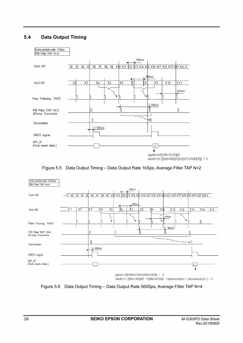
5.4 Data Output Timing
Figure 5.5 Data Output Timing – Data Output Rate 1kSps, Average Filter TAP N=2
Figure 5.6 Data Output Timing – Data Output Rate 500Sps, Average Filter TAP N=4
M-G365PD Data Sheet SEIKO EPSON CORPORATION 17 Rev.20190704
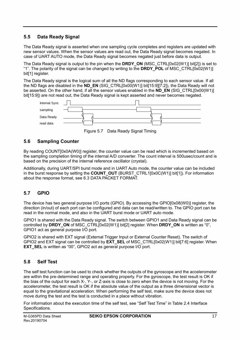
5.5 Data Ready Signal
The Data Ready signal is asserted when one sampling cycle completes and registers are updated with new sensor values. When the sensor values are read out, the Data Ready signal becomes negated. In case of UART AUTO mode, the Data Ready signal becomes negated just before data is output.
The Data Ready signal is output to the pin when the DRDY_ON (MSC_CTRL[0x02(W1)] bit[2]) is set to “1”. The polarity of the signal can be changed by writing to the DRDY_POL of MSC_CTRL[0x02(W1)] bit[1] register.
The Data Ready signal is the logical sum of all the ND flags corresponding to each sensor value. If all the ND flags are disabled in the ND_EN (SIG_CTRL[0x00(W1)] bit[15:9][7:2]), the Data Ready will not be asserted. On the other hand, if all the sensor values enabled in the ND_EN (SIG_CTRL[0x00(W1)] bit[15:9]) are not read out, the Data Ready signal is kept asserted and never becomes negated.
Figure 5.7 Data Ready Signal Timing
5.6 Sampling Counter
By reading COUNT[0x0A(W0)] register, the counter value can be read which is incremented based on the sampling completion timing of the internal A/D converter. The count interval is 500usec/count and is based on the precision of the internal reference oscillator (crystal).
Additionally, during UART/SPI burst mode and in UART Auto mode, the counter value can be included in the burst response by setting the COUNT_OUT (BURST_CTRL1[0x0C(W1)] bit[1]). For information about the response format, see 6.3 DATA PACKET FORMAT.
5.7 GPIO
The device has two general purpose I/O ports (GPIO). By accessing the GPIO[0x08(W0)] register, the direction (in/out) of each port can be configured and data can be read/written to. The GPIO port can be read in the normal mode, and also in the UART burst mode or UART auto mode.
GPIO1 is shared with the Data Ready signal. The switch between GPIO1 and Data Ready signal can be controlled by DRDY_ON of MSC_CTRL[0x02(W1)] bit[2] register. When DRDY_ON is written as “0”, GPIO1 act as general purpose I/O port.
GPIO2 is shared with EXT signal (External Trigger Input or External Counter Reset). The switch of GPIO2 and EXT signal can be controlled by EXT_SEL of MSC_CTRL[0x02(W1)] bit[7:6] register. When EXT_SEL is written as “00”, GPIO2 act as general purpose I/O port.
5.8 Self Test
The self test function can be used to check whether the outputs of the gyroscope and the accelerometer are within the pre-determined range and operating properly. For the gyroscope, the test result is OK if the bias of the output for each X-, Y-, or Z-axis is close to zero when the device is not moving. For the accelerometer, the test result is OK if the absolute value of the output as a three dimensional vector is equal to the gravitational acceleration. When performing the self test, make sure the device does not move during the test and the test is conducted in a place without vibration.
For information about the execution time of the self test, see “Self Test Time” in Table 2.4 Interface Specifications.
Internal Sync
Data Ready
sampling
read data
18 SEIKO EPSON CORPORATION M-G365PD Data Sheet
Rev.20190905
To use the self test function, see the description of the SELF_TEST (MSC_CTRL[0x02(W1)] bit[10]) and the ST_ERR_ALL (DIAG_STAT[0x04(W0)] bit[1]).
NOTE:
When executing the self-test, be sure to disable the external trigger function.
MSC_CTRL[0x02(W1)],bit[7:6]= “00”or“01”
5.9 External Trigger Input
External Trigger Input function provides control of the sample data output timing by using an externally supplied input pulse signal to GPIO2 (EXT) pin. By enabling the EXT_SEL (MSC_CTRL[0x02(W1)] bit[7:6]), GPIO2 pin can be used as External Trigger Input pin. The polarity of External Trigger Input is positive pulse.
To enable the External Trigger Input function, program the settings as shown below:
◼ 100Hz ≦ External Trigger Input frequency < 500Hz
1. Set EXT_SEL to external trigger input by writing “10" to MSC_CTRL[0x02(W1)] bit [7:6]
2. Set EXT_SYNC_ENABLE2 to external trigger input by writing “000" to EXT_SYNC_CTRL[0x19(W1)] bit [10:8] *1
3. Set EXT_SYNC_ENABLE1 to external trigger input by writing “001" to EXT_SYNC_CTRL[0x18(W1)] bit 2:0 *2
4. Set FILTER_SEL to moving average filter TAP=0 by writing “00000" to FILTER_CTRL[0x06(W1)] bit [4:0]
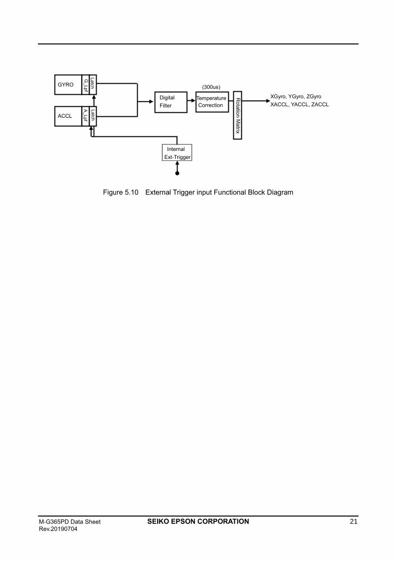
*1) A_Lpf in Figure 5.10 is set to 1.7 Hz (order: 1st)
*2) G_Lpf in Figure 5.10 is set to 9.4 Hz (order: 2nd)
◼ 500Hz ≦ External Trigger Input frequency ≦ 1000Hz
5. Set EXT_SEL to external trigger input by writing “10" to MSC_CTRL[0x02(W1)] bit [7:6]
6. Set EXT_SYNC_ENABLE2 to external trigger input by writing “001" to EXT_SYNC_CTRL[0x19(W1)] bit [10:8] *1
7. Set EXT_SYNC_ENABLE1 to external trigger input by writing “100" to EXT_SYNC_CTRL[0x18(W1)] bit 2:0 *2
8. Set FILTER_SEL to moving average filter TAP=0 by writing “00000" to FILTER_CTRL[0x06(W1)] bit [4:0]
*1) A_Lpf in Figure 5.10 is set to 16.7 Hz (order: 1st)
*2) G_Lpf in Figure 5.10 is set to 94.4 Hz (order: 2nd)
NOTE:
External triggering at frequencies below 100 Hz-signal input is not recommended as it is subject to aliasing effects. If necessary, carefully check the impact before use.
NOTE: To properly disable External Trigger Input function, perform the following steps:
1. Set EXT_SEL to GPIO2 by writing “00" to MSC_CTRL[0x02(W1)] bit [7:6]
2. Set EXT_SYNC_ENABLE2 to disable external trigger input by writing “010" to EXT_SYNC_CTRL[0x19(W1)] bit [10:8] *1
3. Set EXT_SYNC_ENABLE1 to disable trigger input by writing “111" to EXT_SYNC_CTRL[0x18(W1)] bit [2:0] *2
M-G365PD Data Sheet SEIKO EPSON CORPORATION 19 Rev.20190704
4. Set FILTER_SEL to a specified valid setting in FILTER_CTRL[0x06(W1)] bit [4:0] by referring 5.13 Filter.
*1) A_Lpf in Figure 5.10 is set to 167 Hz (order: 1st)
*2) G_Lpf in Figure 5.10 is set to 472 Hz (order: 2nd)
When this function is active, the operation is as follows:
• For UART Auto Mode:
When External Trigger Input pin is asserted, the latest sampling data is set to each register and sent to Host automatically.
• For all other modes:
When External Trigger Input pin is asserted, the latest sampling data is set to each register and Data Ready signal is asserted. The Host should then read the sampling data synchronized with Data Ready signal.
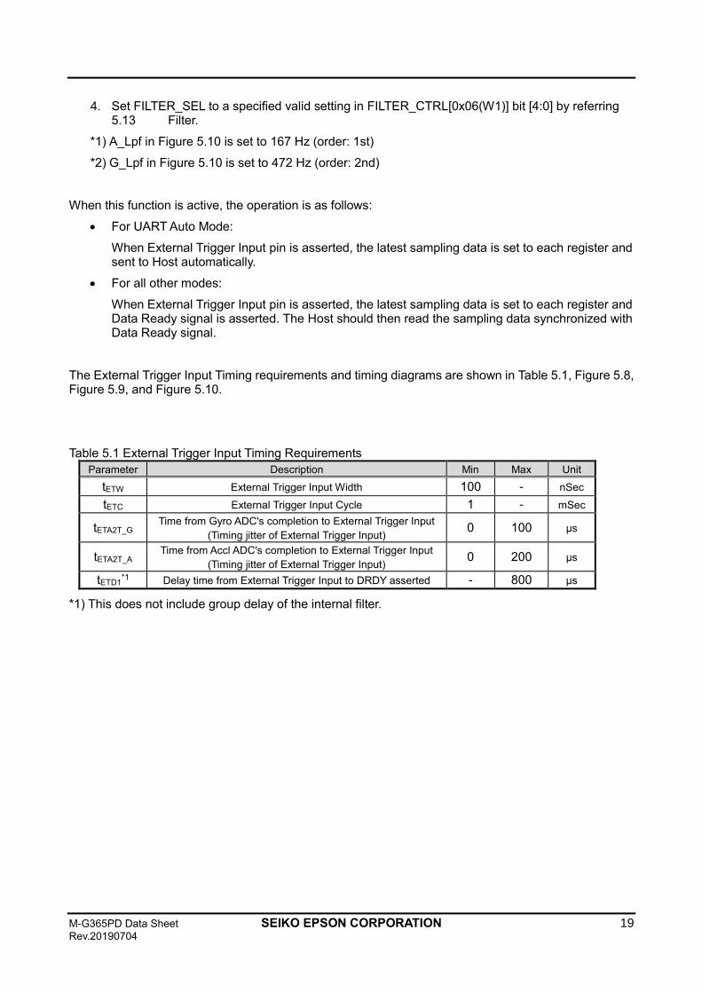
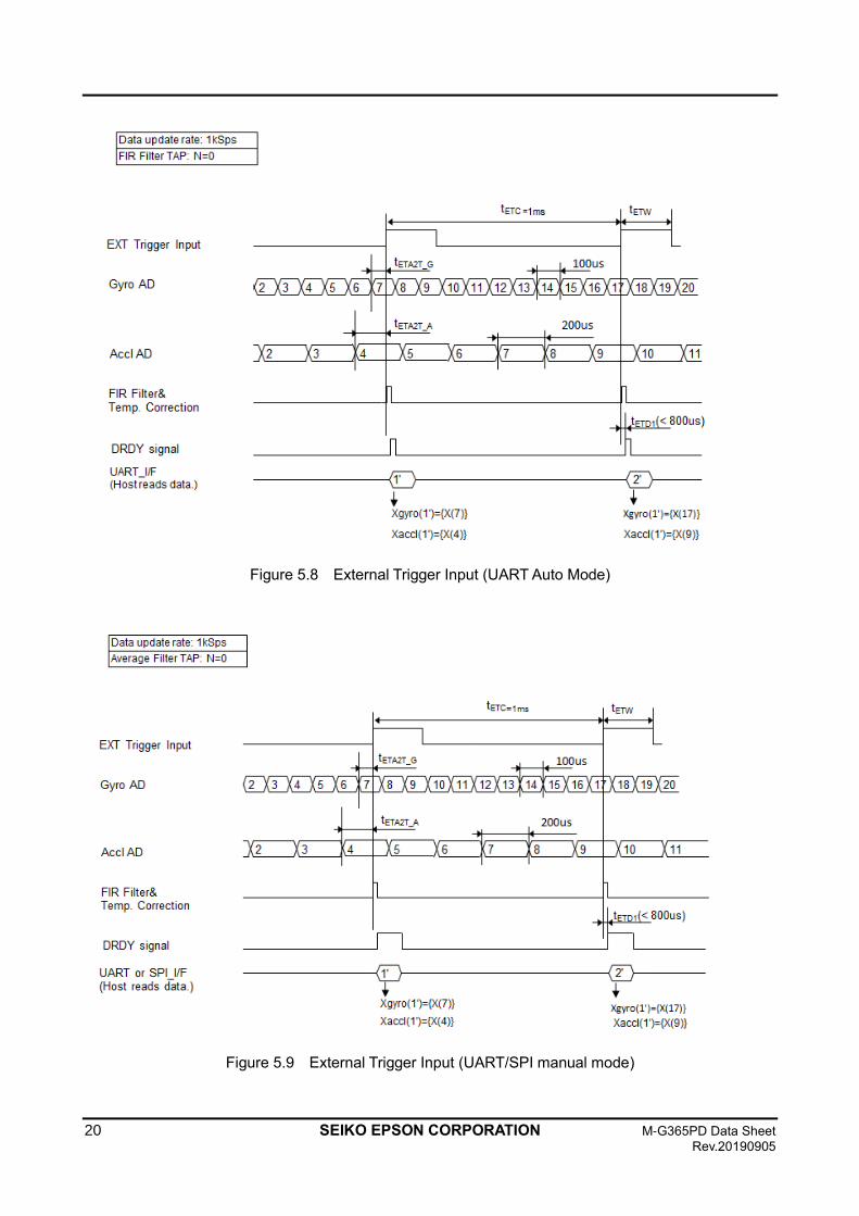
The External Trigger Input Timing requirements and timing diagrams are shown in Table 5.1, Figure 5.8, Figure 5.9, and Figure 5.10.
Table 5.1 External Trigger Input Timing Requirements
Parameter Description Min Max Unit
tETW External Trigger Input Width 100 - nSec
tETC External Trigger Input Cycle 1 - mSec
tETA2T_G Time from Gyro ADC's completion to External Trigger Input
(Timing jitter of External Trigger Input) 0 100 µs
tETA2T_A Time from Accl ADC's completion to External Trigger Input
(Timing jitter of External Trigger Input) 0 200 µs
tETD1*1 Delay time from External Trigger Input to DRDY asserted - 800 µs
*1) This does not include group delay of the internal filter.
20 SEIKO EPSON CORPORATION M-G365PD Data Sheet
Rev.20190905
Figure 5.8 External Trigger Input (UART Auto Mode)
Figure 5.9 External Trigger Input (UART/SPI manual mode)
M-G365PD Data Sheet SEIKO EPSON CORPORATION 21 Rev.20190704
Figure 5.10 External Trigger input Functional Block Diagram
GYRO
ACCL
Digital Filter
Temperature Correction
XGyro, YGyro, ZGyro
XACCL, YACCL, ZACCL
G_L
pf
A_Lpf
Rota
tion M
atrix
(300us)
Latc
h
Internal Ext-Trigger
Latc
h
22 SEIKO EPSON CORPORATION M-G365PD Data Sheet
Rev.20190905
5.10 External Counter Reset Input
The External Counter Reset Input function can be used to measure the time offset from an externally supplied input trigger on GPIO2(EXT) pin to the completion of the next ADC sampling group.
This function is enabled by writing to EXT_SEL (MSC_CTRL [0x02(W1)] bit [7:6]) to select GPIO2 for use as an External Counter Reset Input terminal. The active polarity of the input signal is positive pulse.
The following describes the operation when this function is active:
• The IMU has an internal 16-bit up counter incrementing at 62.5kHz. • The counter begins counting starting from 0 (*1) when Sampling mode begins. The counting
resolution is 16us. • The counter can be reset by assertion of an external signal on the External Counter Reset
Input terminal. After the counter is reset, the count value is cleared and begins incrementing again from 0.
• The counter value is transferred at the time of the ADC sampling completion and stored in COUNT [0x0A(W0)] register before the DataReady signal is asserted.
• The Host can obtain the time offset from External Counter Reset Input signal to ADC sampling completion time by reading the sampling data with the counter value when DataReady signal is asserted.
• The counter value is stopped (*2) when Sampling mode is stopped. • The counter will roll over and increment from 0 again, if the count value increments past
65535. *1) Enter Sampling mode from Configuration mode *2) Leave Sampling mode and enter Configuration mode
NOTE: When the External Counter Reset Input function is enabled, the COUNT [0x0A(W0)] register stores the counter value instead of the sampling count.
The timing specification and timing diagram for the External Counter Reset Input function is shown in Table 5.2 and Figure 5.11.
Table 5.2 External Counter Reset Input Timing
Parameter Description Min Max Unit
tERW External Reset Input Width 100 - nSec
tERC External Reset Input Cycle 1 1000 mSec
tER2A Time from External Reset Input to ADC completion (count*1 x 16) +⊿ER2A μs
⊿ER2A Precision of tER2A -150 150 μs
*1) The count value is read from register COUNT [0x0A(W0)] as indicated.
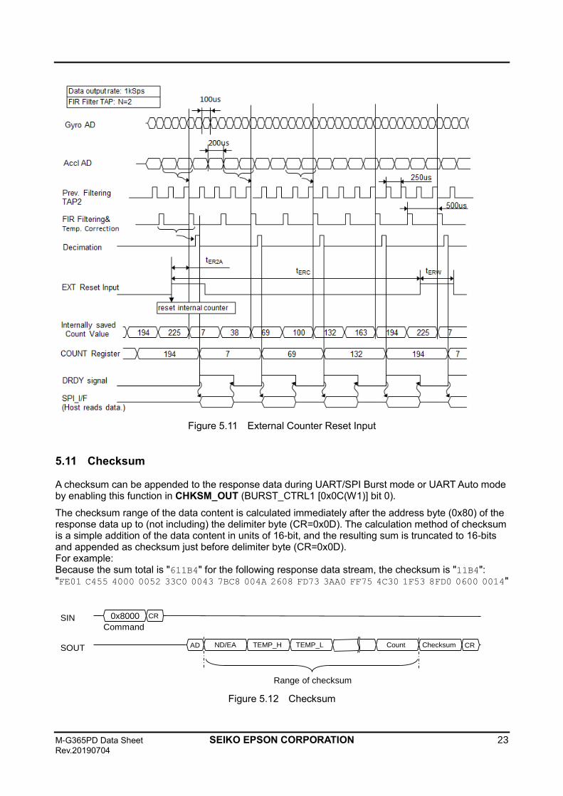
M-G365PD Data Sheet SEIKO EPSON CORPORATION 23 Rev.20190704
Figure 5.11 External Counter Reset Input
5.11 Checksum
A checksum can be appended to the response data during UART/SPI Burst mode or UART Auto mode by enabling this function in CHKSM_OUT (BURST_CTRL1 [0x0C(W1)] bit 0).
The checksum range of the data content is calculated immediately after the address byte (0x80) of the response data up to (not including) the delimiter byte (CR=0x0D). The calculation method of checksum is a simple addition of the data content in units of 16-bit, and the resulting sum is truncated to 16-bits and appended as checksum just before delimiter byte (CR=0x0D). For example: Because the sum total is "611B4" for the following response data stream, the checksum is "11B4": "FE01 C455 4000 0052 33C0 0043 7BC8 004A 2608 FD73 3AA0 FF75 4C30 1F53 8FD0 0600 0014"
Figure 5.12 Checksum
SIN
SOUT
0x8000 CR
Range of checksum
Command
ChecksumCount CRND/EA TEMP_H TEMP_LAD
24 SEIKO EPSON CORPORATION M-G365PD Data Sheet
Rev.20190905
5.12 Automatic Start (For UART Auto Mode Only)
The Automatic Start function when enabled allows the device to automatically enter Sampling Mode after completing internal initialization when power is supplied or the IMU is reset. This function is designed to be used in conjunction with the UART Auto Mode. Please refer to Figure 5.3 for the state transition.
Follow the procedures below to enable the Automatic Start function:
1. Write a “1” to both UART_AUTO (bit 0) and AUTO_START (bit 1) of UART_CTRL [0x08(W1)].
2. Store the current register settings to non-volatile memory by writing a "1" to FLASH_BACKUP (GLOB_CMD [0x0A(W1)] bit 3). After completion of the FLASH_BACKUP command, confirm the results by FLASH_BU_ERR (DIAG_STAT [0x04(W0)] bit 0).
3. The IMU will automatically enter Sampling Mode after the power supply is cycled, or a hardware reset, or a software reset command is executed.
The Automatic Start function can be enabled simultaneously with the External Trigger Input function. Follow the procedures below to enable the Automatic Start with External Trigger Input function:
1. Write a “1” to both UART_AUTO (bit 0) and AUTO_START (bit 1) of UART_CTRL [0x08(W1)].
2. Write a "10" to EXT_SEL (MSC_CTRL [0x02(W1)] bit [7:6]) to enable the External Trigger Input. Please connect the external trigger input signal to the GPIO2 pin.
3. Store the current register settings to non-volatile memory by writing a "1" to FLASH_BACKUP (GLOB_CMD [0x0A(W1)] bit 3). After completion of the FLASH_BACKUP command, confirm the results by FLASH_BU_ERR (DIAG_STAT [0x04(W0)] bit 0).
4. The IMU will automatically enter Sampling Mode after the power supply is cycled, or a hardware reset, or a software reset command is executed.
5.13 Filter
This device contains built-in user configurable digital filters that are applied to the sensor data. The type of filter (moving average filter or FIR Kaiser filter) and the numbers of TAPs can be set with the FILTER_CTRL [0x06(W1)] register.
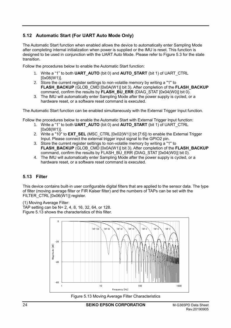
(1) Moving Average Filter: TAP setting can be N= 2, 4, 8, 16, 32, 64, or 128. Figure 5.13 shows the characteristics of this filter.
Figure 5.13 Moving Average Filter Characteristics
-60
-40
-20
0
1 10 100 1000
Frequancy [Hz]
Mag
nitude
[dB
]
TAP:128 TAP:64 TAP:32 TAP:16 TAP:8 TAP:4 TAP:2
M-G365PD Data Sheet SEIKO EPSON CORPORATION 25 Rev.20190704
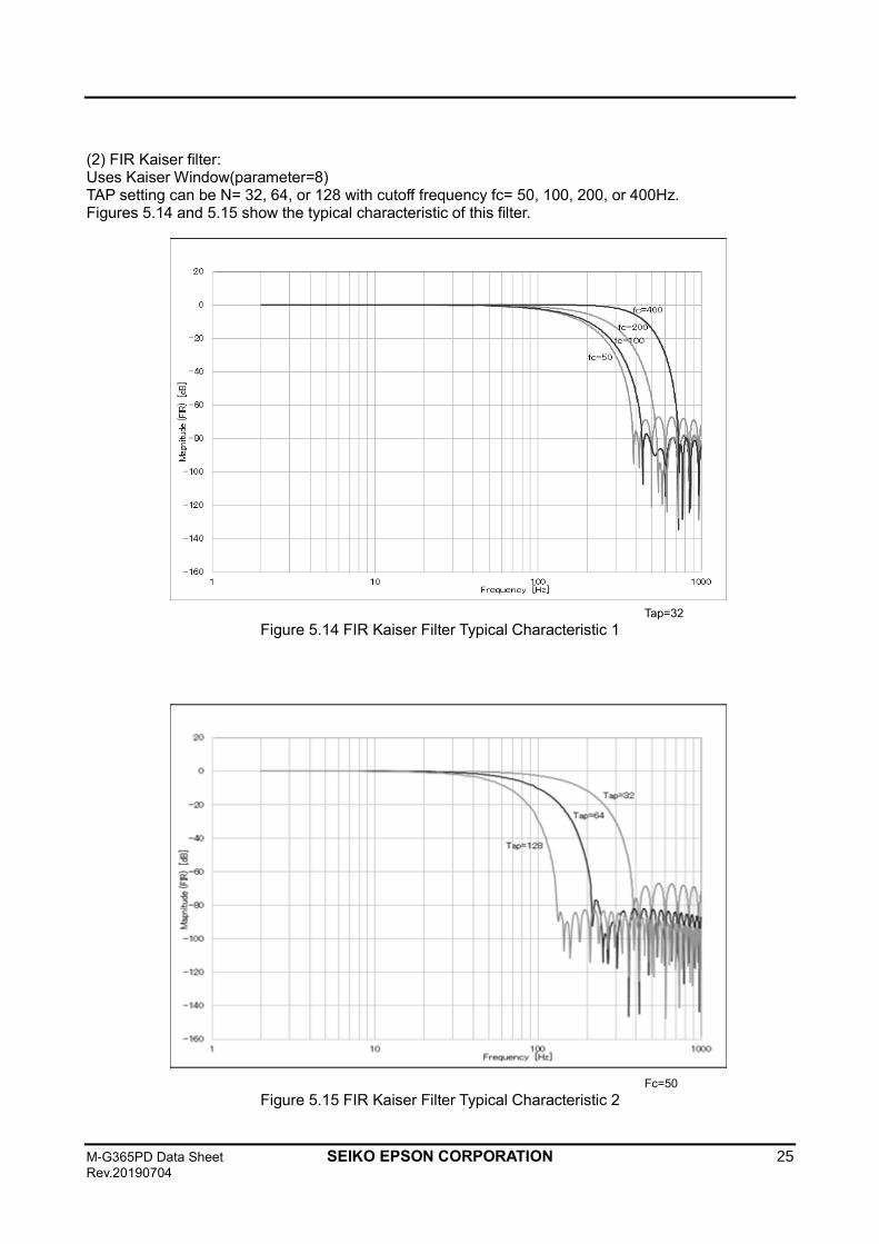
(2) FIR Kaiser filter: Uses Kaiser Window(parameter=8) TAP setting can be N= 32, 64, or 128 with cutoff frequency fc= 50, 100, 200, or 400Hz. Figures 5.14 and 5.15 show the typical characteristic of this filter.
Tap=32
Figure 5.14 FIR Kaiser Filter Typical Characteristic 1
Fc=50
Figure 5.15 FIR Kaiser Filter Typical Characteristic 2
26 SEIKO EPSON CORPORATION M-G365PD Data Sheet
Rev.20190905
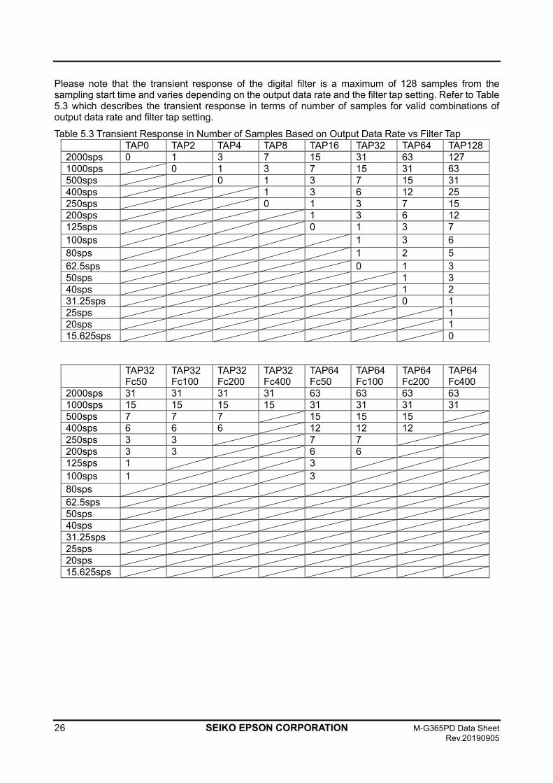
Please note that the transient response of the digital filter is a maximum of 128 samples from the sampling start time and varies depending on the output data rate and the filter tap setting. Refer to Table 5.3 which describes the transient response in terms of number of samples for valid combinations of output data rate and filter tap setting.
Table 5.3 Transient Response in Number of Samples Based on Output Data Rate vs Filter Tap
TAP0 TAP2 TAP4 TAP8 TAP16 TAP32 TAP64 TAP128
2000sps 0 1 3 7 15 31 63 127
1000sps 0 1 3 7 15 31 63
500sps 0 1 3 7 15 31
400sps 1 3 6 12 25
250sps 0 1 3 7 15
200sps 1 3 6 12
125sps 0 1 3 7
100sps 1 3 6
80sps 1 2 5
62.5sps 0 1 3
50sps 1 3
40sps 1 2
31.25sps 0 1
25sps 1
20sps 1
15.625sps 0
TAP32 Fc50
TAP32 Fc100
TAP32 Fc200
TAP32 Fc400
TAP64 Fc50
TAP64 Fc100
TAP64 Fc200
TAP64 Fc400
2000sps 31 31 31 31 63 63 63 63
1000sps 15 15 15 15 31 31 31 31
500sps 7 7 7 15 15 15
400sps 6 6 6 12 12 12
250sps 3 3 7 7
200sps 3 3 6 6
125sps 1 3
100sps 1 3
80sps
62.5sps
50sps
40sps
31.25sps
25sps
20sps
15.625sps
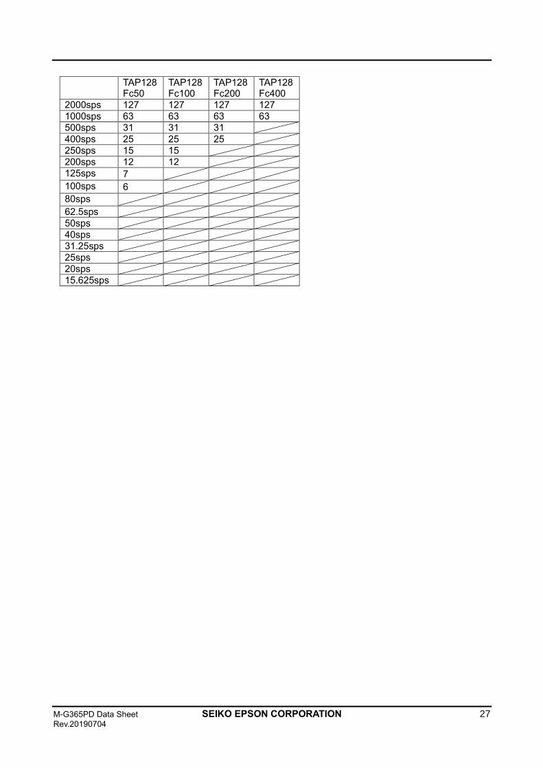
M-G365PD Data Sheet SEIKO EPSON CORPORATION 27 Rev.20190704
TAP128 Fc50
TAP128 Fc100
TAP128 Fc200
TAP128 Fc400
2000sps 127 127 127 127
1000sps 63 63 63 63
500sps 31 31 31
400sps 25 25 25
250sps 15 15
200sps 12 12
125sps 7
100sps 6
80sps
62.5sps
50sps
40sps
31.25sps
25sps
20sps
15.625sps
28 SEIKO EPSON CORPORATION M-G365PD Data Sheet
Rev.20190905
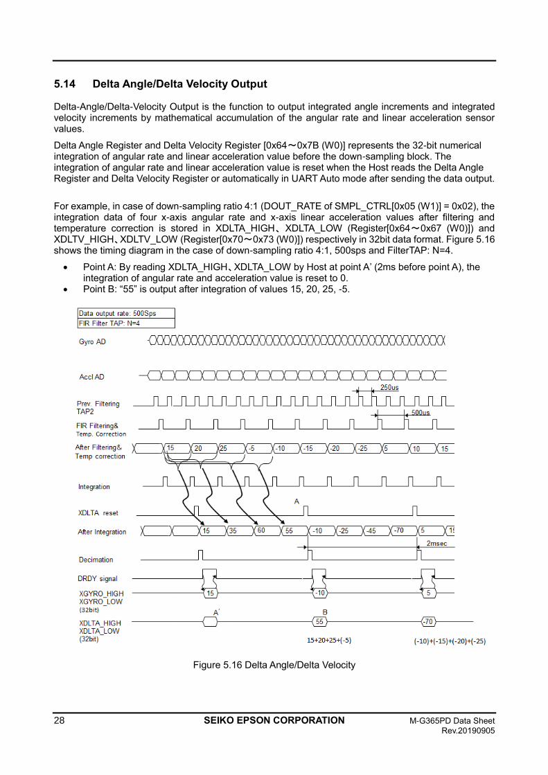
5.14 Delta Angle/Delta Velocity Output
Delta-Angle/Delta-Velocity Output is the function to output integrated angle increments and integrated velocity increments by mathematical accumulation of the angular rate and linear acceleration sensor values.
Delta Angle Register and Delta Velocity Register [0x64~0x7B (W0)] represents the 32-bit numerical integration of angular rate and linear acceleration value before the down-sampling block. The integration of angular rate and linear acceleration value is reset when the Host reads the Delta Angle Register and Delta Velocity Register or automatically in UART Auto mode after sending the data output.
For example, in case of down-sampling ratio 4:1 (DOUT_RATE of SMPL_CTRL[0x05 (W1)] = 0x02), the integration data of four x-axis angular rate and x-axis linear acceleration values after filtering and temperature correction is stored in XDLTA_HIGH、XDLTA_LOW (Register[0x64~0x67 (W0)]) and XDLTV_HIGH、XDLTV_LOW (Register[0x70~0x73 (W0)]) respectively in 32bit data format. Figure 5.16 shows the timing diagram in the case of down-sampling ratio 4:1, 500sps and FilterTAP: N=4.
• Point A: By reading XDLTA_HIGH、XDLTA_LOW by Host at point A’ (2ms before point A), the integration of angular rate and acceleration value is reset to 0.
• Point B: “55” is output after integration of values 15, 20, 25, -5.
Figure 5.16 Delta Angle/Delta Velocity

M-G365PD Data Sheet SEIKO EPSON CORPORATION 29 Rev.20190704
As described above, the numerical integration of angular rate and linear acceleration values is reset by reading Delta Angle Register and Delta Velocity Register by Host or automatically in UART Auto mode after sending the data output. However when selecting 16bit output mode in DLTA_BIT of BURST_CTRL2[0x0E(W1)] bit 11 or DLTV_BIT of BURST_CTRL2[0x0E(W1)] bit 10, the upper 16bit of the value will be output and lower 16bit will be added to the next integration cycle.
NOTE: Delta Angle/Delta Velocity output is restricted and not supported for SPI normal mode reads.
30 SEIKO EPSON CORPORATION M-G365PD Data Sheet
Rev.20190905
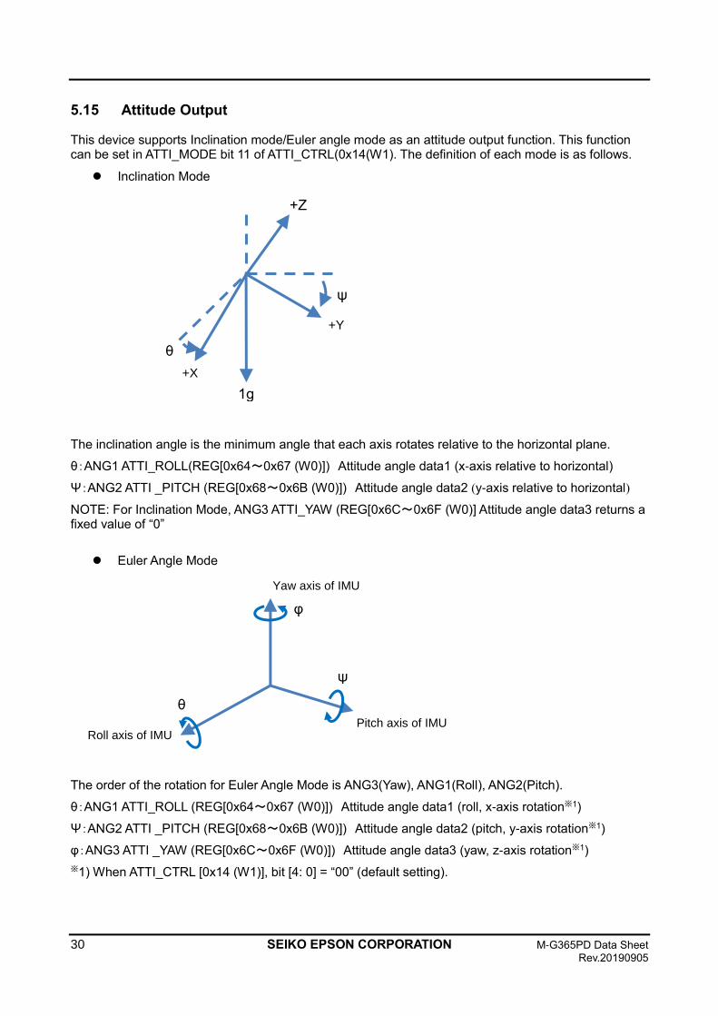
5.15 Attitude Output
This device supports Inclination mode/Euler angle mode as an attitude output function. This function can be set in ATTI_MODE bit 11 of ATTI_CTRL(0x14(W1). The definition of each mode is as follows.
⚫ Inclination Mode
The inclination angle is the minimum angle that each axis rotates relative to the horizontal plane.
θ:ANG1 ATTI_ROLL(REG[0x64~0x67 (W0)]) Attitude angle data1 (x-axis relative to horizontal)
Ψ:ANG2 ATTI _PITCH (REG[0x68~0x6B (W0)]) Attitude angle data2 (y-axis relative to horizontal)
NOTE: For Inclination Mode, ANG3 ATTI_YAW (REG[0x6C~0x6F (W0)] Attitude angle data3 returns a fixed value of “0”
⚫ Euler Angle Mode
The order of the rotation for Euler Angle Mode is ANG3(Yaw), ANG1(Roll), ANG2(Pitch).
θ:ANG1 ATTI_ROLL (REG[0x64~0x67 (W0)]) Attitude angle data1 (roll, x-axis rotation※1)
Ψ:ANG2 ATTI _PITCH (REG[0x68~0x6B (W0)]) Attitude angle data2 (pitch, y-axis rotation※1)
φ:ANG3 ATTI _YAW (REG[0x6C~0x6F (W0)]) Attitude angle data3 (yaw, z-axis rotation※1)
※1) When ATTI_CTRL [0x14 (W1)], bit [4: 0] = “00” (default setting).
Yaw axis of IMU
φ
θ
ψ
Pitch axis of IMU Roll axis of IMU
+Y
+X
+Z
ψ
θ
1g
M-G365PD Data Sheet SEIKO EPSON CORPORATION 31 Rev.20190704
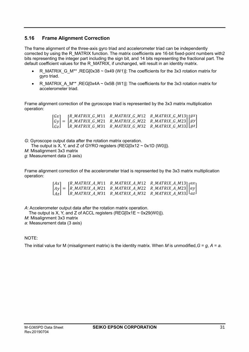
5.16 Frame Alignment Correction
The frame alignment of the three-axis gyro triad and accelerometer triad can be independently corrected by using the R_MATRIX function. The matrix coefficients are 16-bit fixed-point numbers with2 bits representing the integer part including the sign bit, and 14 bits representing the fractional part. The default coefficient values for the R_MATRIX, if unchanged, will result in an identity matrix.
• R_MATRIX_G_M** ,REG[0x38 ~ 0x49 (W1)]: The coefficients for the 3x3 rotation matrix for gyro triad.
• R_MATRIX_A_M** ,REG[0x4A ~ 0x5B (W1)]: The coefficients for the 3x3 rotation matrix for accelerometer triad.
Frame alignment correction of the gyroscope triad is represented by the 3x3 matrix multiplication operation:
[𝐺𝑥𝐺𝑦𝐺𝑧
] = [𝑅_𝑀𝐴𝑇𝑅𝐼𝑋_𝐺_𝑀11 𝑅_𝑀𝐴𝑇𝑅𝐼𝑋_𝐺_𝑀12 𝑅_𝑀𝐴𝑇𝑅𝐼𝑋_𝐺_𝑀13𝑅_𝑀𝐴𝑇𝑅𝐼𝑋_𝐺_𝑀21 𝑅_𝑀𝐴𝑇𝑅𝐼𝑋_𝐺_𝑀22 𝑅_𝑀𝐴𝑇𝑅𝐼𝑋_𝐺_𝑀23𝑅_𝑀𝐴𝑇𝑅𝐼𝑋_𝐺_𝑀31 𝑅_𝑀𝐴𝑇𝑅𝐼𝑋_𝐺_𝑀32 𝑅_𝑀𝐴𝑇𝑅𝐼𝑋_𝐺_𝑀33
] [
𝑔𝑥𝑔𝑦𝑔𝑧
]
G: Gyroscope output data after the rotation matrix operation. The output is X, Y, and Z of GYRO registers (REG[0x12 ~ 0x1D (W0)]). M: Misalignment 3x3 matrix g: Measurement data (3 axis)
Frame alignment correction of the accelerometer triad is represented by the 3x3 matrix multiplication operation:
[𝐴𝑥𝐴𝑦𝐴𝑧
] = [𝑅_𝑀𝐴𝑇𝑅𝐼𝑋_𝐴_𝑀11 𝑅_𝑀𝐴𝑇𝑅𝐼𝑋_𝐴_𝑀12 𝑅_𝑀𝐴𝑇𝑅𝐼𝑋_𝐴_𝑀13𝑅_𝑀𝐴𝑇𝑅𝐼𝑋_𝐴_𝑀21 𝑅_𝑀𝐴𝑇𝑅𝐼𝑋_𝐴_𝑀22 𝑅_𝑀𝐴𝑇𝑅𝐼𝑋_𝐴_𝑀23𝑅_𝑀𝐴𝑇𝑅𝐼𝑋_𝐴_𝑀31 𝑅_𝑀𝐴𝑇𝑅𝐼𝑋_𝐴_𝑀32 𝑅_𝑀𝐴𝑇𝑅𝐼𝑋_𝐴_𝑀33
] [𝑎𝑥𝑎𝑦𝑎𝑧
]
A: Accelerometer output data after the rotation matrix operation. The output is X, Y, and Z of ACCL registers (REG[0x1E ~ 0x29(W0)]). M: Misalignment 3x3 matrix a: Measurement data (3 axis)
NOTE:
The initial value for M (misalignment matrix) is the identity matrix. When M is unmodified,G = g, A = a.
32 SEIKO EPSON CORPORATION M-G365PD Data Sheet
Rev.20190905
6. Digital Interface
This device has the following two external interfaces.
(1) SPI interface
(2) UART interface
The SPI interface and the UART interface have almost the same functions, except additionally the UART interface supports Auto Mode function. Because both interfaces are always active, the user needs only to connect the desired interface pins SPI or UART, without needing any hardware pin configuration or selection.
NOTE: Connecting both SPI and UART at the same time is not supported and may result in malfunction of the device.
The registers inside the device are accessed via the SPI or UART interfaces.
In this document, data sent to the device is called a “Command” and data sent back in response to the command is called a “Response”. There are two types of commands: write command and read command. The write command has no response. The write command always writes to the internal register in 8-bit words. The response to the read command, i.e. the data from the internal register, is always read in 16-bit words.
When reading from the registers, there is a special mode called the burst mode in addition to the normal mode.
When the IMU output data rate is high (i.e. 1000sps), it is possible to exceed the bandwidth of the host interface and cause the data transmission to be incorrect. In this case, the user must balance the transmission data rate and the bandwidth capability of the host interface.
Adjust the following settings accordingly to optimize the host interface bandwidth: • For the UART, adjust the baud rate in BAUD_RATE (UART_CTRL [0x08(W1)] bit 8). • For the SPI, adjust the host side SPI clock frequency and SPI wait time.
Adjust the following settings accordingly to optimize the transmission data rate:
• The transmission data rate is affected by the data output rate setting in DOUT_RATE (SMPL_CTRL [0x04(W1)] bits [15:8]).
• The transmission data rate is also affected by the number of output bytes included in burst mode read transfer. The adjustment to the number of output bytes is in registers BURST_CTRL1 [0x0C(W1)] and BURST_CTRL2 [0x0E(W1)].
Several concrete examples for setting the transmission data rate and host interface bandwidth are shown below:
(1) For UART and 32-bit output:
Baudrate: 921600 Baud, Data output rate: 2000sps
• BAUD_RATE =“10" of UART_CTRL [0x08(W1)] bit[9:8]: 921600 baud
• UART_AUTO =“1" of UART_CTRL [0x08(W1)] bit [0]: UART Auto Mode
• DOUT_RATE = 0x00 of SMPL_CTRL [0x04(W1)] bit [15:8]: 2000Sps
• BURST_CTRL1 [0x0C(W1)] = 0xF006: FLAG, TEMP, angle rate, acceleration, GPIO, and COUNT output
• BURST_CTRL2 [0x0E(W1)] = 0x7000: TEMP, angle rate, and acceleration output are 32-bit.
Baudrate: 460800 Baud, Data output rate: 1000sps
• BAUD_RATE =“00" of UART_CTRL [0x08(W1)] bit[9:8]: 460800 baud
• UART_AUTO =“1" of UART_CTRL [0x08(W1)] bit [0]: UART Auto Mode
• DOUT_RATE = 0x01 of SMPL_CTRL [0x04(W1)] bit [15:8]: 1000Sps
• BURST_CTRL1 [0x0C(W1)] = 0xF006: FLAG, TEMP, angle rate, acceleration, GPIO, and COUNT output
• BURST_CTRL2 [0x0E(W1)] = 0x7000: TEMP, angle rate, and acceleration output are 32-bit.
(2) For SPI and 32-bit output:
• SPI Interface Transmission Setting: FSCLK=1MHz and tSTALL=24us for normal mode
M-G365PD Data Sheet SEIKO EPSON CORPORATION 33 Rev.20190704
• DOUT_RATE = 0x01 of SMPL_CTRL [0x04(W1)] bit [15:8]: 1000Sps
• BURST_CTRL1 [0x0C(W1)] = 0xF006: FLAG, TEMP, angle rate, acceleration, GPIO, and COUNT output
• BURST_CTRL2 [0x0E(W1)] = 0x7000: TEMP, angle rate, and acceleration output are 32-bit.
(3) For UART and 16-bit output:
• BAUD_RATE =“00" of UART_CTRL [0x08(W1)] bit[9:8]: 460800 baud
• UART_AUTO =“1" of UART_CTRL [0x08(W1)] bit [0]: UART Auto Mode
• DOUT_RATE = 0x01 of SMPL_CTRL [0x04(W1)] bit [15:8]: 1000Sps
• BURST_CTRL1 [0x0C(W1)] = 0xF006: FLAG, TEMP, angle rate, acceleration, GPIO, and COUNT output
• BURST_CTRL2 [0x0E(W1)] = 0x0000: TEMP, angle rate, and acceleration output are 16-bit.
(4) For SPI and 16-bit output:
• SPI Interface Transmission Setting: FSCLK=1MHz and tSTALL=24us for normal mode
• DOUT_RATE = 0x01 of SMPL_CTRL [0x04(W1)] bit [15:8]: 1000Sps
• BURST_CTRL1 [0x0C(W1)] = 0xF006: FLAG, TEMP, angle rate, acceleration, GPIO, and COUNT output
• BURST_CTRL2 [0x0E(W1)] = 0x0000: All TEMP, angle rate, and acceleration output are 16-bit.
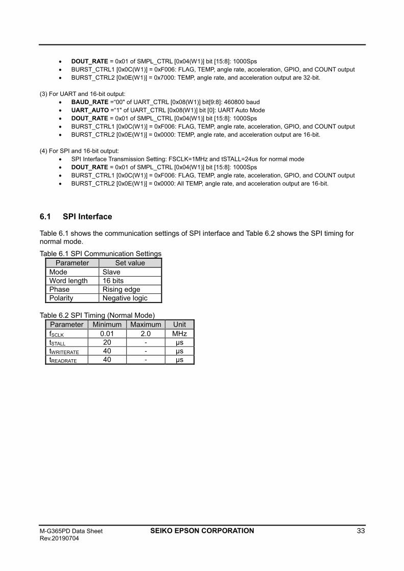
6.1 SPI Interface
Table 6.1 shows the communication settings of SPI interface and Table 6.2 shows the SPI timing for normal mode.
Table 6.1 SPI Communication Settings
Parameter Set value
Mode Slave
Word length 16 bits
Phase Rising edge
Polarity Negative logic
Table 6.2 SPI Timing (Normal Mode)
Parameter Minimum Maximum Unit
fSCLK 0.01 2.0 MHz
tSTALL 20 - μs
tWRITERATE 40 - μs
tREADRATE 40 - μs
34 SEIKO EPSON CORPORATION M-G365PD Data Sheet
Rev.20190905
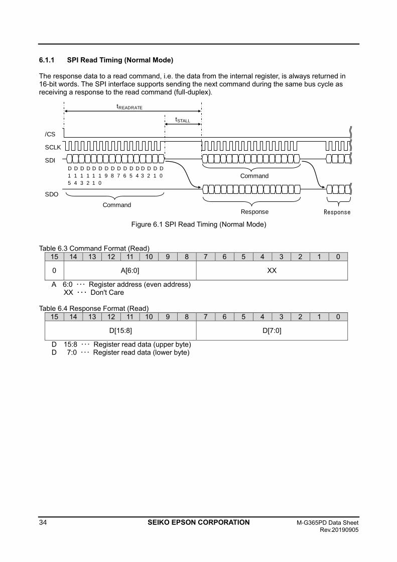
6.1.1 SPI Read Timing (Normal Mode)
The response data to a read command, i.e. the data from the internal register, is always returned in 16-bit words. The SPI interface supports sending the next command during the same bus cycle as receiving a response to the read command (full-duplex).
Figure 6.1 SPI Read Timing (Normal Mode)
Table 6.3 Command Format (Read)
15 14 13 12 11 10 9 8 7 6 5 4 3 2 1 0
0 A[6:0] XX
A 6:0 ・・・ Register address (even address) XX ・・・ Don't Care
Table 6.4 Response Format (Read)
15 14 13 12 11 10 9 8 7 6 5 4 3 2 1 0
D[15:8] D[7:0]
D 15:8 ・・・ Register read data (upper byte) D 7:0 ・・・ Register read data (lower byte)
SCLK
SDO
SDI
/CS
CommandResponse
tREADRATE
tSTALL
Command
Response
D
1
5
D
1
4
D
1
3
D
1
2
D
1
1
D
1
0
D
9
D
8
D
7
D
6
D
5
D
4
D
3
D
2
D
1
D
0
M-G365PD Data Sheet SEIKO EPSON CORPORATION 35 Rev.20190704
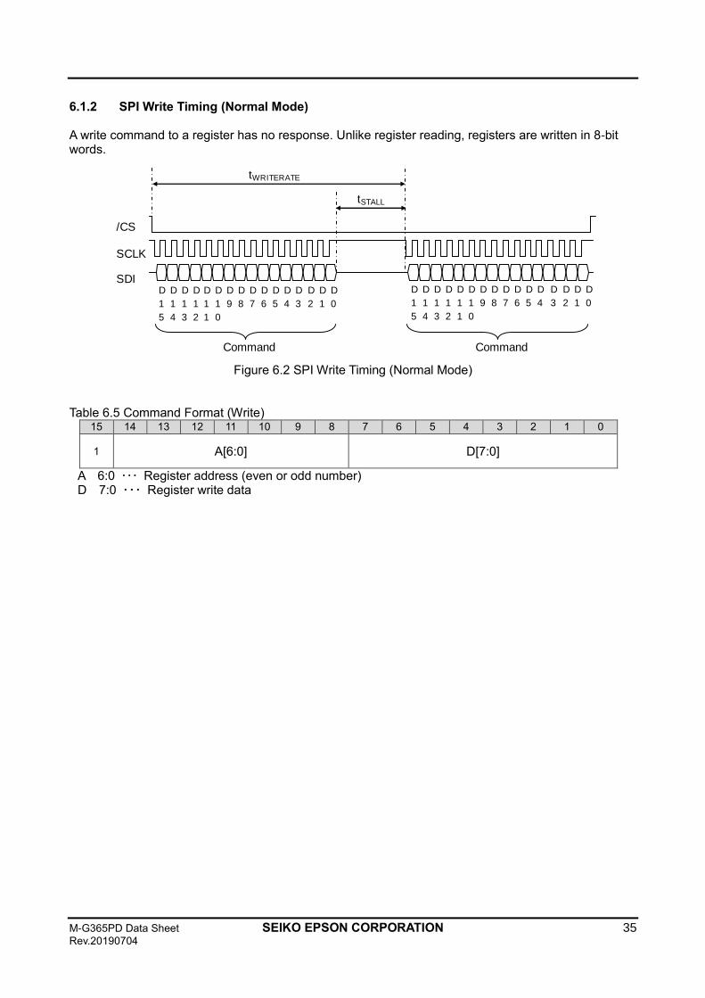
6.1.2 SPI Write Timing (Normal Mode)
A write command to a register has no response. Unlike register reading, registers are written in 8-bit words.
Figure 6.2 SPI Write Timing (Normal Mode)
Table 6.5 Command Format (Write) 15 14 13 12 11 10 9 8 7 6 5 4 3 2 1 0
1 A[6:0] D[7:0]
A 6:0 ・・・ Register address (even or odd number) D 7:0 ・・・ Register write data
SCLK
SDI
/CS
tWRITERATE
tSTALL
D
1
5
D
1
4
D
1
3
D
1
2
D
1
1
D
1
0
D
9
D
8
D
7
D
6
D
5
D
4
D
3
D
2
D
1
D
0
Command Command
D
1
5
D
1
4
D
1
3
D
1
2
D
1
1
D
1
0
D
9
D
8
D
7
D
6
D
5
D
4
D
3
D
2
D
1
D
0
36 SEIKO EPSON CORPORATION M-G365PD Data Sheet
Rev.20190905
6.1.3 SPI Read Timing (Burst Mode)
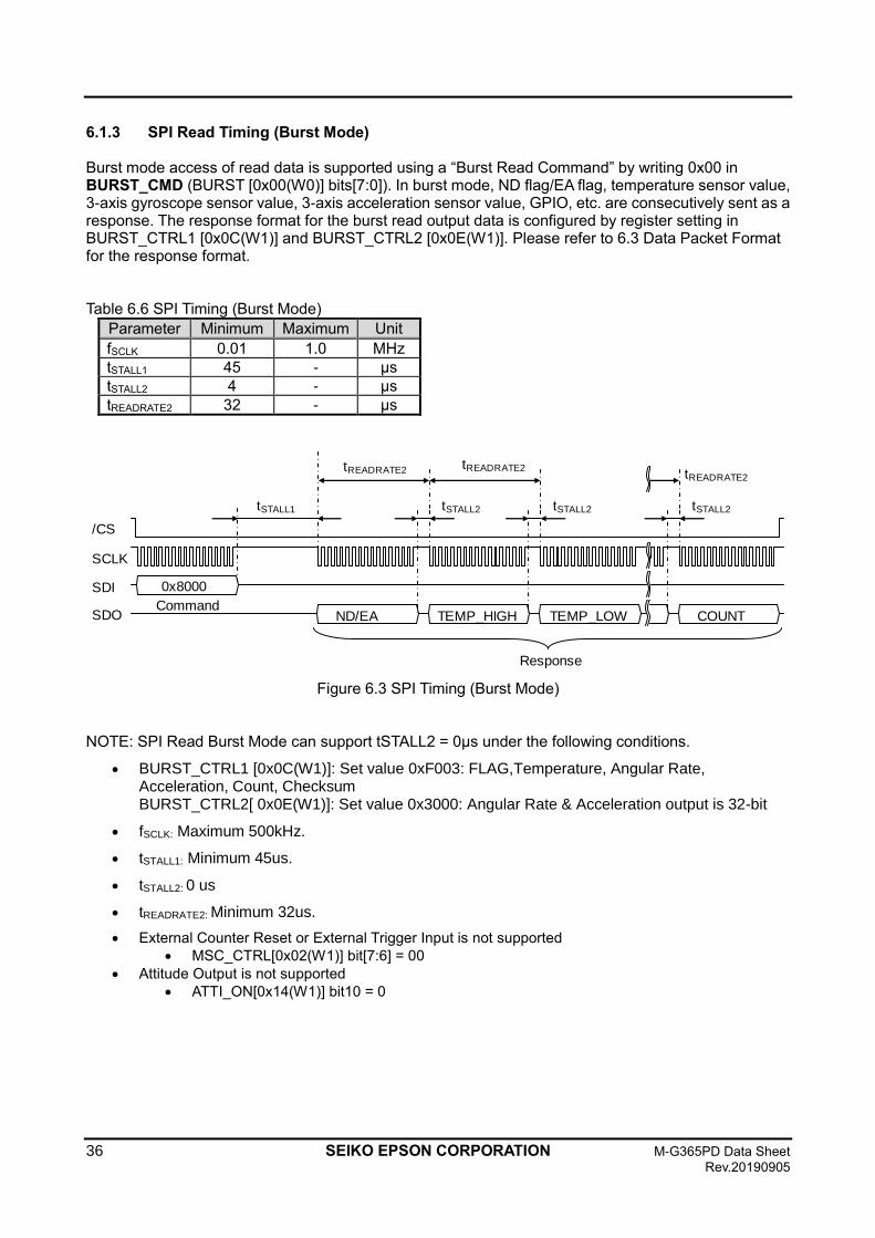
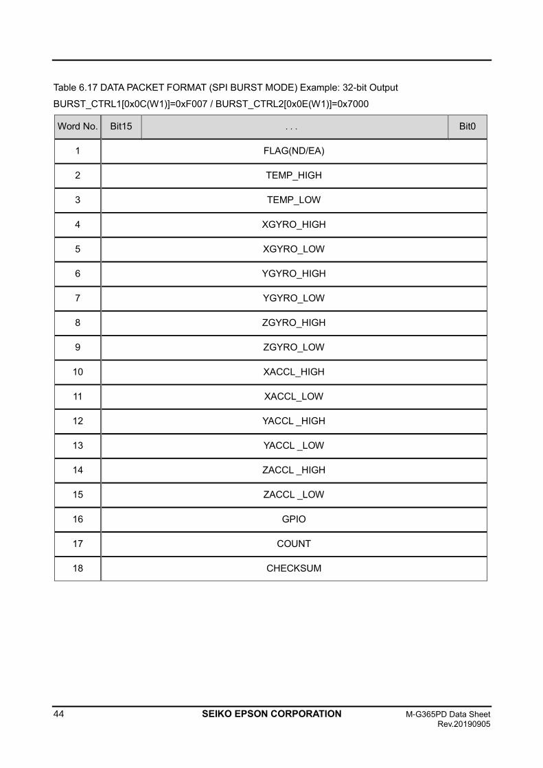
Burst mode access of read data is supported using a “Burst Read Command” by writing 0x00 in BURST_CMD (BURST [0x00(W0)] bits[7:0]). In burst mode, ND flag/EA flag, temperature sensor value, 3-axis gyroscope sensor value, 3-axis acceleration sensor value, GPIO, etc. are consecutively sent as a response. The response format for the burst read output data is configured by register setting in BURST_CTRL1 [0x0C(W1)] and BURST_CTRL2 [0x0E(W1)]. Please refer to 6.3 Data Packet Format for the response format.
Table 6.6 SPI Timing (Burst Mode)
Parameter Minimum Maximum Unit
fSCLK 0.01 1.0 MHz
tSTALL1 45 - μs
tSTALL2 4 - μs
tREADRATE2 32 - μs
Figure 6.3 SPI Timing (Burst Mode)
NOTE: SPI Read Burst Mode can support tSTALL2 = 0μs under the following conditions.
• BURST_CTRL1 [0x0C(W1)]: Set value 0xF003: FLAG,Temperature, Angular Rate, Acceleration, Count, Checksum BURST_CTRL2[ 0x0E(W1)]: Set value 0x3000: Angular Rate & Acceleration output is 32-bit
• fSCLK: Maximum 500kHz.
• tSTALL1: Minimum 45us.
• tSTALL2: 0 us
• tREADRATE2: Minimum 32us.
• External Counter Reset or External Trigger Input is not supported • MSC_CTRL[0x02(W1)] bit[7:6] = 00
• Attitude Output is not supported • ATTI_ON[0x14(W1)] bit10 = 0
/CS
tSTALL1 tSTALL2
tREADRATE2
Response
SCLK
SDO
SDI
CommandND/EA TEMP_HIGH TEMP_LOW COUNT
tSTALL2tSTALL2
tREADRATE2tREADRATE2
0x8000
M-G365PD Data Sheet SEIKO EPSON CORPORATION 37 Rev.20190704
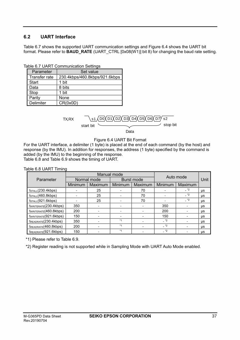
6.2 UART Interface
Table 6.7 shows the supported UART communication settings and Figure 6.4 shows the UART bit format. Please refer to BAUD_RATE (UART_CTRL [0x08(W1)] bit 8) for changing the baud rate setting.
Table 6.7 UART Communication Settings
Parameter Set value
Transfer rate 230.4kbps/460.8kbps/921.6kbps
Start 1 bit
Data 8 bits
Stop 1 bit
Parity None
Delimiter CR(0x0D)
Figure 6.4 UART Bit Format For the UART interface, a delimiter (1 byte) is placed at the end of each command (by the host) and response (by the IMU). In addition for responses, the address (1 byte) specified by the command is added (by the IMU) to the beginning of the response. Table 6.8 and Table 6.9 shows the timing of UART. Table 6.8 UART Timing
Parameter
Manual mode Auto mode
Unit Normal mode Burst mode
Minimum Maximum Minimum Maximum Minimum Maximum
tSTALL(230.4kbps) - 25 - 70 - - *2 μs
tSTALL(460.8kbps) - 25 - 70 - - *2 μs
tSTALL(921.6kbps) - 25 - 70 - - *2 µs
tWRITERATE(230.4kbps) 350 - - - 350 - μs
tWRITERATE(460.8kbps) 200 - - - 200 - μs
tWRITERATE(921.6kbps) 150 - - - 150 - µs
tREADRATE(230.4kbps) 350 - *1 - - *2 - μs
tREADRATE(460.8kbps) 200 - *1 - - *2 - μs
tREADRATE(921.6kbps) 150 - *1 - - *2 - µs
*1) Please refer to Table 6.9.
*2) Register reading is not supported while in Sampling Mode with UART Auto Mode enabled.
TX,RX s1 D0 D1 D2 D3 D4 D5 D6 D7 s2
start bit stop bit
Data
38 SEIKO EPSON CORPORATION M-G365PD Data Sheet
Rev.20190905
Table 6.9 UART Timing (tREADRATE requirements for Burst Mode)
Parameter Burst Mode (minimum) Unit
tREADRATE(230.4kbps) 300 + ( 43.4 * B ) μs
tREADRATE(460.8kbps) 200 + ( 21.7 * B ) μs
tREADRATE(921.6kbps) 150 + ( 10.9 * B ) µs
B= Number of receive data bytes (AD: address and CR: delimiter is not included).
Example tREADRATE Calculation:
BURST_CTRL1 [0x0C(W1)]: Set value 0xF006 BURST_CTRL2[ 0x0E(W1)]: Set value 0x7000 B=34 byte for the above stated register setting tREADRATE(460.8kbps) = 200 + (21.7 * 34) = 937.8(μs)
6.2.1 UART Read Timing (Normal Mode)
The response to the read command, i.e. the data from the internal register, is always returned 16-bit data at a time. The register address (AD) comes at the beginning of the response, for example, 0x02 for the MODE_CTRL [0x02(W0)] register.
Figure 6.5 UART Read Timing (Normal Mode)
Table 6.10 Command Format (Read)
First byte Second byte Third byte
7 6 5 4 3 2 1 0 7 6 5 4 3 2 1 0 7 6 5 4 3 2 1 0
0 A[6:0] XX 0x0D
A[6:0] ・・・ Register address (even address) XX ・・・ Don't Care 0x0D ・・・ Delimiter
Table 6.11 Response Format (Read)
First byte Second byte Third byte Fourth byte
7 6 5 4 3 2 1 0 7 6 5 4 3 2 1 0 7 6 5 4 3 2 1 0 7 6 5 4 3 2 1 0
0 A[6:0] D[15:8] D[7:0] 0x0D
A[6:0] ・・・ Register address (even address) D[15:8] ・・・ Register read data (upper byte) D[7:0] ・・・ Register read data (lower byte) 0x0D ・・・ Delimiter
SIN
SOUT
Command CR Command CR
Response CRAD Response CRAD
tREADRATE
tSTALL
M-G365PD Data Sheet SEIKO EPSON CORPORATION 39 Rev.20190704
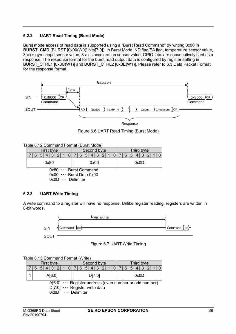
6.2.2 UART Read Timing (Burst Mode)
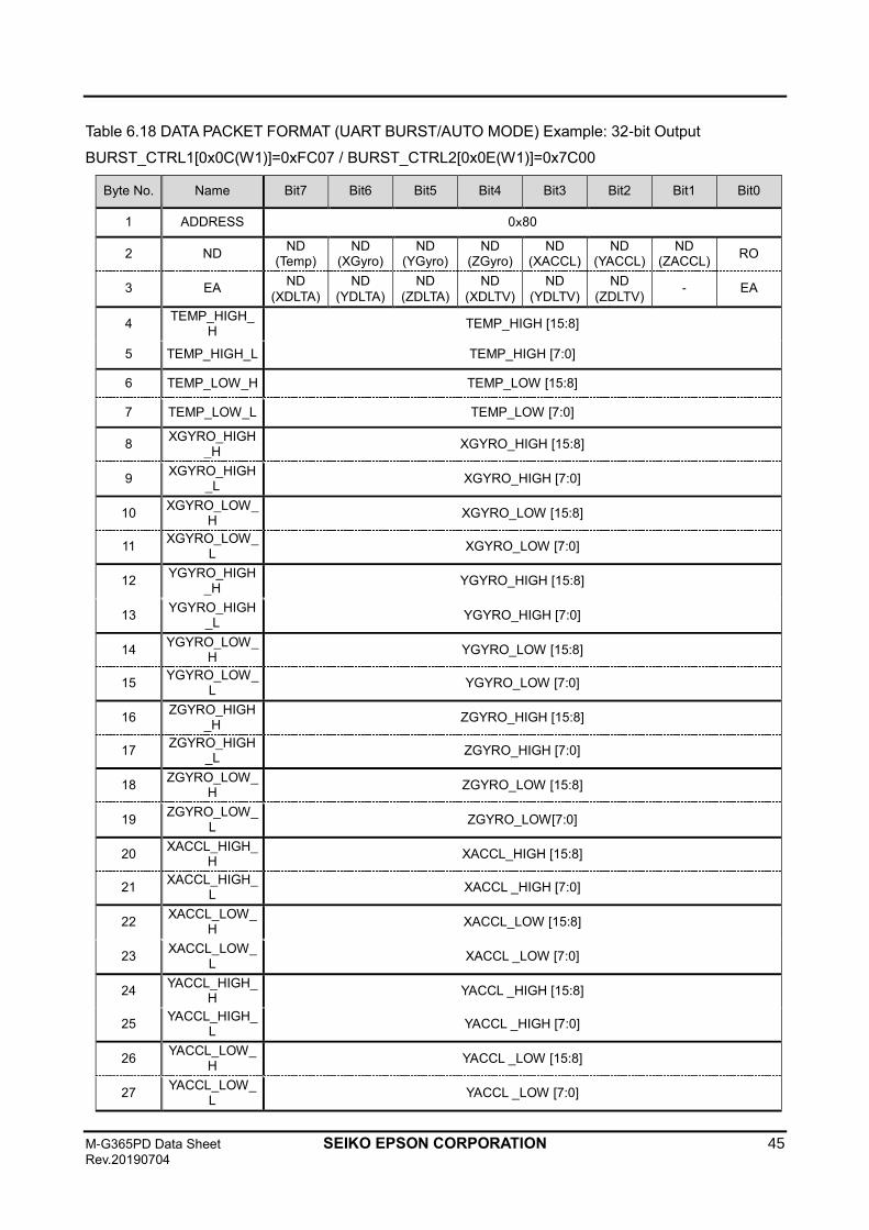
Burst mode access of read data is supported using a “Burst Read Command” by writing 0x00 in BURST_CMD (BURST [0x00(W0)] bits[7:0]). In Burst Mode, ND flag/EA flag, temperature sensor value, 3-axis gyroscope sensor value, 3-axis acceleration sensor value, GPIO, etc. are consecutively sent as a response. The response format for the burst read output data is configured by register setting in BURST_CTRL1 [0x0C(W1)] and BURST_CTRL2 [0x0E(W1)]. Please refer to 6.3 Data Packet Format for the response format.
Figure 6.6 UART Read Timing (Burst Mode)
Table 6.12 Command Format (Burst Mode)
First byte Second byte Third byte
7 6 5 4 3 2 1 0 7 6 5 4 3 2 1 0 7 6 5 4 3 2 1 0
0x80 0x00 0x0D
0x80 ・・・ Burst Command 0x00 ・・・ Burst Data 0x00 0x0D ・・・ Delimiter
6.2.3 UART Write Timing
A write command to a register will have no response. Unlike register reading, registers are written in 8-bit words.
Figure 6.7 UART Write Timing
Table 6.13 Command Format (Write)
First byte Second byte Third byte
7 6 5 4 3 2 1 0 7 6 5 4 3 2 1 0 7 6 5 4 3 2 1 0
1 A[6:0] D[7:0] 0x0D
A[6:0] ・・・ Register address (even number or odd number) D[7:0] ・・・ Register write data 0x0D ・・・ Delimiter
tREADRATE
tSTALL
Response
SIN
SOUT
0x8000 CR
Command
ChecksumCount CRND/EA TEMP_HAD
0x8000 CR
Command
SIN
SOUT
Command CR Command CR
tWRITERATE
40 SEIKO EPSON CORPORATION M-G365PD Data Sheet
Rev.20190905
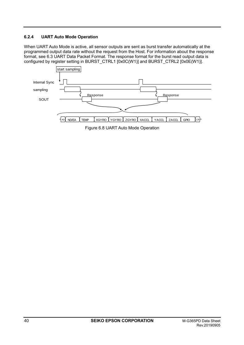
6.2.4 UART Auto Mode Operation
When UART Auto Mode is active, all sensor outputs are sent as burst transfer automatically at the programmed output data rate without the request from the Host. For information about the response format, see 6.3 UART Data Packet Format. The response format for the burst read output data is configured by register setting in BURST_CTRL1 [0x0C(W1)] and BURST_CTRL2 [0x0E(W1)].
Figure 6.8 UART Auto Mode Operation
Internal Sync
sampling
SOUT
start sampling
Response Response
ND/EAAD TEMP XGYRO YGYRO ZGYRO XACCL YACCL ZACCL GPIO CR
M-G365PD Data Sheet SEIKO EPSON CORPORATION 41 Rev.20190704
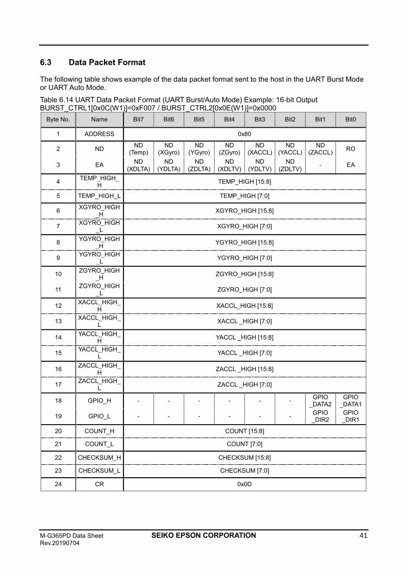
6.3 Data Packet Format
The following table shows example of the data packet format sent to the host in the UART Burst Mode or UART Auto Mode.
Table 6.14 UART Data Packet Format (UART Burst/Auto Mode) Example: 16-bit Output BURST_CTRL1[0x0C(W1)]=0xF007 / BURST_CTRL2[0x0E(W1)]=0x0000
Byte No. Name Bit7 Bit6 Bit5 Bit4 Bit3 Bit2 Bit1 Bit0
1 ADDRESS 0x80
2 ND ND
(Temp) ND
(XGyro) ND
(YGyro) ND
(ZGyro) ND
(XACCL) ND
(YACCL) ND
(ZACCL) RO
3 EA ND
(XDLTA)
ND
(YDLTA)
ND
(ZDLTA)
ND
(XDLTV)
ND
(YDLTV)
ND
(ZDLTV) - EA
4 TEMP_HIGH_
H TEMP_HIGH [15:8]
5 TEMP_HIGH_L TEMP_HIGH [7:0]
6 XGYRO_HIGH
_H XGYRO_HIGH [15:8]
7 XGYRO_HIGH
_L XGYRO_HIGH [7:0]
8 YGYRO_HIGH
_H YGYRO_HIGH [15:8]
9 YGYRO_HIGH
_L YGYRO_HIGH [7:0]
10 ZGYRO_HIGH
_H ZGYRO_HIGH [15:8]
11 ZGYRO_HIGH
_L ZGYRO_HIGH [7:0]
12 XACCL_HIGH_
H XACCL_HIGH [15:8]
13 XACCL_HIGH_
L XACCL _HIGH [7:0]
14 YACCL_HIGH_
H YACCL _HIGH [15:8]
15 YACCL_HIGH_
L YACCL _HIGH [7:0]
16 ZACCL_HIGH_
H ZACCL _HIGH [15:8]
17 ZACCL_HIGH_
L ZACCL _HIGH [7:0]
18 GPIO_H - - - - - - GPIO
_DATA2 GPIO
_DATA1
19 GPIO_L - - - - - - GPIO _DIR2
GPIO _DIR1
20 COUNT_H COUNT [15:8]
21 COUNT_L COUNT [7:0]
22 CHECKSUM_H CHECKSUM [15:8]
23 CHECKSUM_L CHECKSUM [7:0]
24 CR 0x0D
42 SEIKO EPSON CORPORATION M-G365PD Data Sheet
Rev.20190905
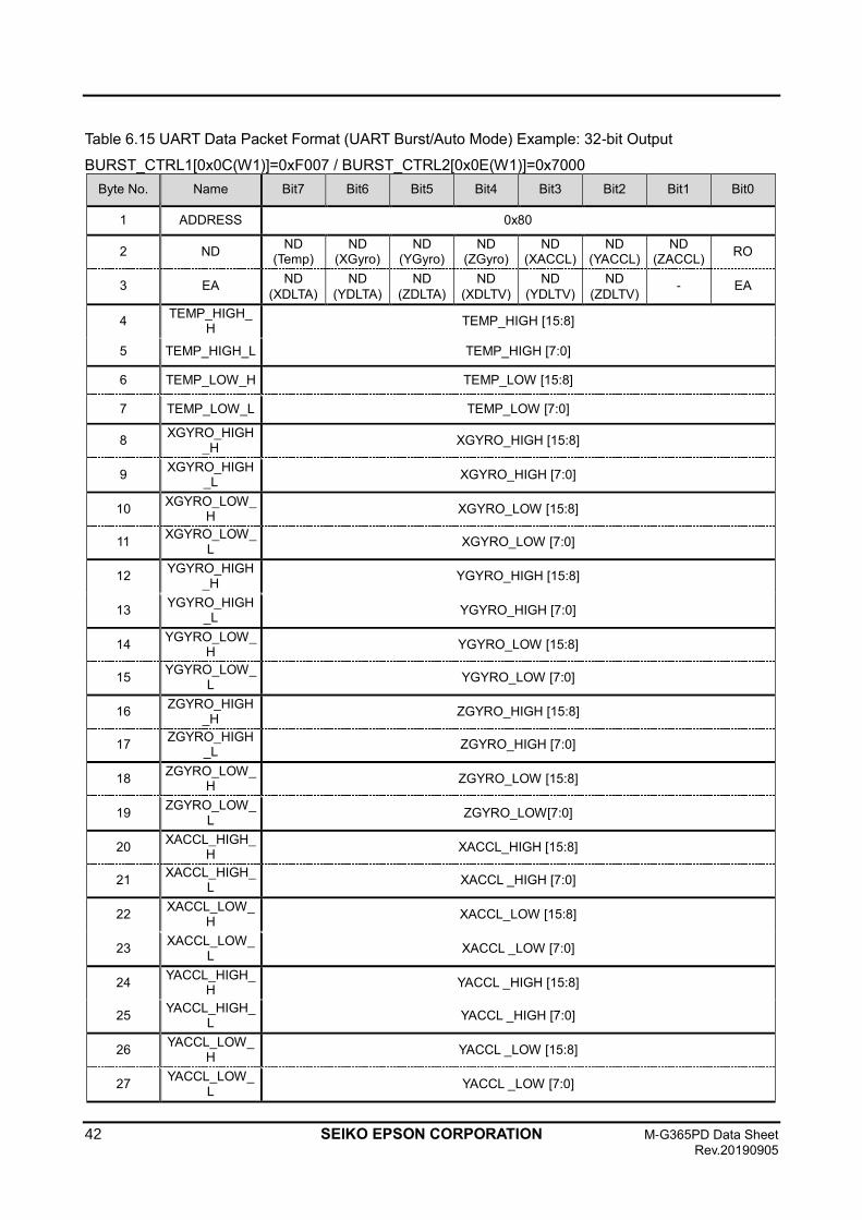
Table 6.15 UART Data Packet Format (UART Burst/Auto Mode) Example: 32-bit Output
BURST_CTRL1[0x0C(W1)]=0xF007 / BURST_CTRL2[0x0E(W1)]=0x7000
Byte No. Name Bit7 Bit6 Bit5 Bit4 Bit3 Bit2 Bit1 Bit0
1 ADDRESS 0x80
2 ND ND
(Temp) ND
(XGyro) ND
(YGyro) ND
(ZGyro) ND
(XACCL) ND
(YACCL) ND
(ZACCL) RO
3 EA ND
(XDLTA)
ND
(YDLTA)
ND
(ZDLTA)
ND
(XDLTV)
ND
(YDLTV)
ND
(ZDLTV) - EA
4 TEMP_HIGH_
H TEMP_HIGH [15:8]
5 TEMP_HIGH_L TEMP_HIGH [7:0]
6 TEMP_LOW_H TEMP_LOW [15:8]
7 TEMP_LOW_L TEMP_LOW [7:0]
8 XGYRO_HIGH
_H XGYRO_HIGH [15:8]
9 XGYRO_HIGH
_L XGYRO_HIGH [7:0]
10 XGYRO_LOW_
H XGYRO_LOW [15:8]
11 XGYRO_LOW_
L XGYRO_LOW [7:0]
12 YGYRO_HIGH
_H YGYRO_HIGH [15:8]
13 YGYRO_HIGH
_L YGYRO_HIGH [7:0]
14 YGYRO_LOW_
H YGYRO_LOW [15:8]
15 YGYRO_LOW_
L YGYRO_LOW [7:0]
16 ZGYRO_HIGH
_H ZGYRO_HIGH [15:8]
17 ZGYRO_HIGH
_L ZGYRO_HIGH [7:0]
18 ZGYRO_LOW_
H ZGYRO_LOW [15:8]
19 ZGYRO_LOW_
L ZGYRO_LOW[7:0]
20 XACCL_HIGH_
H XACCL_HIGH [15:8]
21 XACCL_HIGH_
L XACCL _HIGH [7:0]
22 XACCL_LOW_
H XACCL_LOW [15:8]
23 XACCL_LOW_
L XACCL _LOW [7:0]
24 YACCL_HIGH_
H YACCL _HIGH [15:8]
25 YACCL_HIGH_
L YACCL _HIGH [7:0]
26 YACCL_LOW_
H YACCL _LOW [15:8]
27 YACCL_LOW_
L YACCL _LOW [7:0]
M-G365PD Data Sheet SEIKO EPSON CORPORATION 43 Rev.20190704
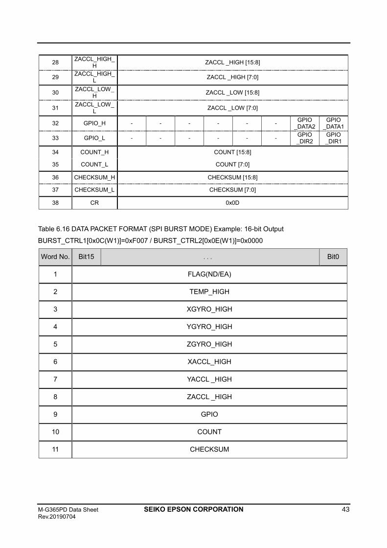
28 ZACCL_HIGH_
H ZACCL _HIGH [15:8]
29 ZACCL_HIGH_
L ZACCL _HIGH [7:0]
30 ZACCL_LOW_
H ZACCL _LOW [15:8]
31 ZACCL_LOW_
L ZACCL _LOW [7:0]
32 GPIO_H - - - - - - GPIO
_DATA2 GPIO
_DATA1
33 GPIO_L - - - - - - GPIO _DIR2
GPIO _DIR1
34 COUNT_H COUNT [15:8]
35 COUNT_L COUNT [7:0]
36 CHECKSUM_H CHECKSUM [15:8]
37 CHECKSUM_L CHECKSUM [7:0]
38 CR 0x0D
Table 6.16 DATA PACKET FORMAT (SPI BURST MODE) Example: 16-bit Output
BURST_CTRL1[0x0C(W1)]=0xF007 / BURST_CTRL2[0x0E(W1)]=0x0000
Word No. Bit15 ... Bit0
1 FLAG(ND/EA)
2 TEMP_HIGH
3 XGYRO_HIGH
4 YGYRO_HIGH
5 ZGYRO_HIGH
6 XACCL_HIGH
7 YACCL _HIGH
8 ZACCL _HIGH
9 GPIO
10 COUNT
11 CHECKSUM
44 SEIKO EPSON CORPORATION M-G365PD Data Sheet
Rev.20190905
Table 6.17 DATA PACKET FORMAT (SPI BURST MODE) Example: 32-bit Output
BURST_CTRL1[0x0C(W1)]=0xF007 / BURST_CTRL2[0x0E(W1)]=0x7000
Word No. Bit15 ... Bit0
1 FLAG(ND/EA)
2 TEMP_HIGH
3 TEMP_LOW
4 XGYRO_HIGH
5 XGYRO_LOW
6 YGYRO_HIGH
7 YGYRO_LOW
8 ZGYRO_HIGH
9 ZGYRO_LOW
10 XACCL_HIGH
11 XACCL_LOW
12 YACCL _HIGH
13 YACCL _LOW
14 ZACCL _HIGH
15 ZACCL _LOW
16 GPIO
17 COUNT
18 CHECKSUM
M-G365PD Data Sheet SEIKO EPSON CORPORATION 45 Rev.20190704
Table 6.18 DATA PACKET FORMAT (UART BURST/AUTO MODE) Example: 32-bit Output
BURST_CTRL1[0x0C(W1)]=0xFC07 / BURST_CTRL2[0x0E(W1)]=0x7C00
Byte No. Name Bit7 Bit6 Bit5 Bit4 Bit3 Bit2 Bit1 Bit0
1 ADDRESS 0x80
2 ND ND
(Temp) ND
(XGyro) ND
(YGyro) ND
(ZGyro) ND
(XACCL) ND
(YACCL) ND
(ZACCL) RO
3 EA ND
(XDLTA)
ND
(YDLTA)
ND
(ZDLTA)
ND
(XDLTV)
ND
(YDLTV)
ND
(ZDLTV) - EA
4 TEMP_HIGH_
H TEMP_HIGH [15:8]
5 TEMP_HIGH_L TEMP_HIGH [7:0]
6 TEMP_LOW_H TEMP_LOW [15:8]
7 TEMP_LOW_L TEMP_LOW [7:0]
8 XGYRO_HIGH
_H XGYRO_HIGH [15:8]
9 XGYRO_HIGH
_L XGYRO_HIGH [7:0]
10 XGYRO_LOW_
H XGYRO_LOW [15:8]
11 XGYRO_LOW_
L XGYRO_LOW [7:0]
12 YGYRO_HIGH
_H YGYRO_HIGH [15:8]
13 YGYRO_HIGH
_L YGYRO_HIGH [7:0]
14 YGYRO_LOW_
H YGYRO_LOW [15:8]
15 YGYRO_LOW_
L YGYRO_LOW [7:0]
16 ZGYRO_HIGH
_H ZGYRO_HIGH [15:8]
17 ZGYRO_HIGH
_L ZGYRO_HIGH [7:0]
18 ZGYRO_LOW_
H ZGYRO_LOW [15:8]
19 ZGYRO_LOW_
L ZGYRO_LOW[7:0]
20 XACCL_HIGH_
H XACCL_HIGH [15:8]
21 XACCL_HIGH_
L XACCL _HIGH [7:0]
22 XACCL_LOW_
H XACCL_LOW [15:8]
23 XACCL_LOW_
L XACCL _LOW [7:0]
24 YACCL_HIGH_
H YACCL _HIGH [15:8]
25 YACCL_HIGH_
L YACCL _HIGH [7:0]
26 YACCL_LOW_
H YACCL _LOW [15:8]
27 YACCL_LOW_
L YACCL _LOW [7:0]
46 SEIKO EPSON CORPORATION M-G365PD Data Sheet
Rev.20190905
28 ZACCL_HIGH_
H ZACCL _HIGH [15:8]
29 ZACCL_HIGH_
L ZACCL _HIGH [7:0]
30 ZACCL_LOW_
H ZACCL _LOW [15:8]
31 ZACCL_LOW_
L ZACCL _LOW [7:0]
32 XDLTA_HIGH_
H XDLTA_HIGH [15:8]
33 XDLTA_HIGH_
L XDLTA_HIGH [7:0]
34 XDLTA_LOW_
H XDLTA_LOW [15:8]
35 XDLTA_LOW_L XDLTA_LOW [7:0]
36 YDLTA_HIGH_
H YDLTA_HIGH [15:8]
37 YDLTA_HIGH_
L YDLTA_HIGH [7:0]
38 YDLTA_LOW_
H YDLTA_LOW [15:8]
39 YDLTA_LOW_L YDLTA_LOW [7:0]
40 ZDLTA_HIGH_
H ZDLTA_HIGH [15:8]
41 ZDLTA_HIGH_
L ZDLTA_HIGH [7:0]
42 ZDLTA_LOW_
H ZDLTA_LOW [15:8]
43 ZDLTA_LOW_L ZDLTA_LOW[7:0]
44 XDLTV_HIGH_
H XDLTV_HIGH [15:8]
45 XDLTV_HIGH_
L XDLTV_HIGH [7:0]
46 XDLTV_LOW_
H XDLTV_LOW [15:8]
47 XDLTV_LOW_L XDLTV_LOW [7:0]
48 YDLTV_HIGH_
H YDLTV_HIGH [15:8]
49 YDLTV_HIGH_
L YDLTV_HIGH [7:0]
50 YDLTV_LOW_
H YDLTV_LOW [15:8]
51 YDLTV_LOW_L YDLTV_LOW [7:0]
52 ZDLTV_HIGH_
H ZDLTV_HIGH [15:8]
53 ZDLTV_HIGH_
L ZDLTV_HIGH [7:0]
54 ZDLTV_LOW_
H ZDLTV_LOW [15:8]
55 ZDLTV_LOW_L ZDLTV_LOW[7:0]
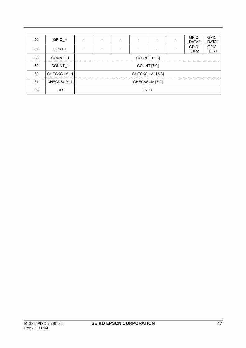
M-G365PD Data Sheet SEIKO EPSON CORPORATION 47 Rev.20190704
56 GPIO_H - - - - - - GPIO
_DATA2 GPIO
_DATA1
57 GPIO_L - - - - - - GPIO _DIR2
GPIO _DIR1
58 COUNT_H COUNT [15:8]
59 COUNT_L COUNT [7:0]
60 CHECKSUM_H CHECKSUM [15:8]
61 CHECKSUM_L CHECKSUM [7:0]
62 CR 0x0D

48 SEIKO EPSON CORPORATION M-G365PD Data Sheet
Rev.20190905
Table 6.19 UART Data Packet Format (UART Burst/Auto Mode) Example: 32-bit Output
BURST_CTRL1[0x0C(W1)]=0xF107 / BURST_CTRL2[0x0E(W1)]=0x7100
Byte No. Name Bit7 Bit6 Bit5 Bit4 Bit3 Bit2 Bit1 Bit0
1 ADDRESS 0x80
2 ND ND
(Temp) ND
(XGyro) ND
(YGyro) ND
(ZGyro) ND
(XACCL) ND
(YACCL) ND
(ZACCL) RO
3 EA ND
(XDLTA)
ND
(YDLTA)
ND
(ZDLTA)
ND
(XDLTV)
ND
(YDLTV)
ND
(ZDLTV) - EA
4 TEMP_ HIGH_H
TEMP_HIGH [15:8]
5 TEMP_ HIGH_L
TEMP_HIGH [7:0]
6 TEMP_ LOW_H
TEMP_LOW [15:8]
7 TEMP_ LOW_L
TEMP_LOW [7:0]
8 XGYRO_ HIGH_H
XGYRO_HIGH [15:8]
9 XGYRO
_HIGH_L XGYRO_HIGH [7:0]
10 XGYRO_ LOW_H
XGYRO_LOW [15:8]
11 XGYRO _LOW_L
XGYRO_LOW [7:0]
12 YGYRO
_HIGH_H YGYRO_HIGH [15:8]
13 YGYRO
_HIGH_L YGYRO_HIGH [7:0]
14 YGYRO _LOW_H
YGYRO_LOW [15:8]
15 YGYRO _LOW_L
YGYRO_LOW [7:0]
16 ZGYRO
_HIGH_H ZGYRO_HIGH [15:8]
17 ZGYRO
_HIGH_L ZGYRO_HIGH [7:0]
18 ZGYRO
_LOW_H ZGYRO_LOW [15:8]
19 ZGYRO _LOW_L
ZGYRO_LOW[7:0]
20 XACCL
_HIGH_H XACCL_HIGH [15:8]
21 XACCL
_HIGH_L XACCL_HIGH [7:0]
22 XACCL
_LOW_H XACCL_LOW [15:8]
23 XACCL
_LOW_L XACCL_LOW [7:0]
24 YACCL
_HIGH_H YACCL_HIGH [15:8]
25 YACCL
_HIGH_L YACCL_HIGH [7:0]
26 YACCL
_LOW_H YACCL_LOW [15:8]
27 YACCL YACCL_LOW [7:0]
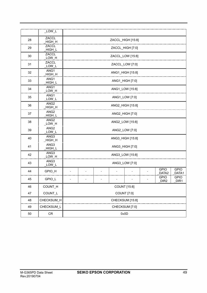
M-G365PD Data Sheet SEIKO EPSON CORPORATION 49 Rev.20190704
_LOW_L
28 ZACCL
_HIGH_H ZACCL_HIGH [15:8]
29 ZACCL
_HIGH_L ZACCL_HIGH [7:0]
30 ZACCL
_LOW_H ZACCL_LOW [15:8]
31 ZACCL
_LOW_L ZACCL_LOW [7:0]
32 ANG1
_HIGH_H ANG1_HIGH [15:8]
33 ANG1
_HIGH_L ANG1_HIGH [7:0]
34 ANG1
_LOW_H ANG1_LOW [15:8]
35 ANG1
_LOW_L ANG1_LOW [7:0]
36 ANG2
_HIGH_H ANG2_HIGH [15:8]
37 ANG2
_HIGH_L ANG2_HIGH [7:0]
38 ANG2
_LOW_H ANG2_LOW [15:8]
39 ANG2
_LOW_L ANG2_LOW [7:0]
40 ANG3
_HIGH_H ANG3_HIGH [15:8]
41 ANG3
_HIGH_L ANG3_HIGH [7:0]
42 ANG3
_LOW_H ANG3_LOW [15:8]
43 ANG3
_LOW_L ANG3_LOW [7:0]
44 GPIO_H - - - - - - GPIO
_DATA2 GPIO
_DATA1
45 GPIO_L - - - - - - GPIO _DIR2
GPIO _DIR1
46 COUNT_H COUNT [15:8]
47 COUNT_L COUNT [7:0]
48 CHECKSUM_H CHECKSUM [15:8]
49 CHECKSUM_L CHECKSUM [7:0]
50 CR 0x0D
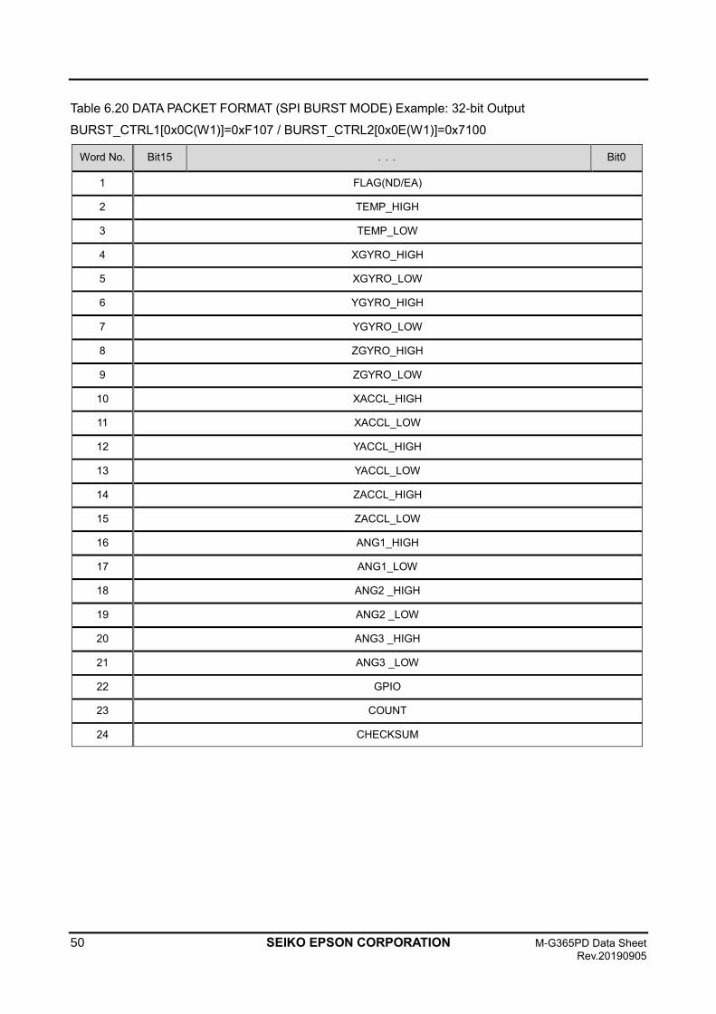
50 SEIKO EPSON CORPORATION M-G365PD Data Sheet
Rev.20190905
Table 6.20 DATA PACKET FORMAT (SPI BURST MODE) Example: 32-bit Output
BURST_CTRL1[0x0C(W1)]=0xF107 / BURST_CTRL2[0x0E(W1)]=0x7100
Word No. Bit15 ... Bit0
1 FLAG(ND/EA)
2 TEMP_HIGH
3 TEMP_LOW
4 XGYRO_HIGH
5 XGYRO_LOW
6 YGYRO_HIGH
7 YGYRO_LOW
8 ZGYRO_HIGH
9 ZGYRO_LOW
10 XACCL_HIGH
11 XACCL_LOW
12 YACCL_HIGH
13 YACCL_LOW
14 ZACCL_HIGH
15 ZACCL_LOW
16 ANG1_HIGH
17 ANG1_LOW
18 ANG2 _HIGH
19 ANG2 _LOW
20 ANG3 _HIGH
21 ANG3 _LOW
22 GPIO
23 COUNT
24 CHECKSUM
M-G365PD Data Sheet SEIKO EPSON CORPORATION 51 Rev.20190704
7. User Registers
A host device (for example, a microcontroller) can control the IMU by accessing the control registers inside the device.
The registers are accessed in this device using a WINDOW method. The prescribed window number is first written to WINDOW_ID of WIN_CTRL[0x7E(W0/W1)] bit [7:0], then the desired register address can be accessed. The WIN_CTRL [0x7E(W0/W1)] register can always be accessed without needing to set the window number.
During the Power-On Start-Up Time or the Reset Recovery time specified in the Table 2.4 Interface Specifications, all the register values are undefined because internal initialization is in progress. Ensure the IMU registers are only accessed after the Power-On Start-Up Time is over.
For information about the initial values of the control registers after internal initialization is finished, see the “Default” column in the Table 7.1. The control registers with ○ mark in the “Flash Backup” column can be saved to the non-volatile memory by the user, and the initial values after the power on will be the values read from the non-volatile memory. If the read out from the non-volatile memory fails, the FLASH_ERR (DIAG_STAT [0x04(W0)] bit[2]) is set to 1 (error).
Please ensure that the IMU is in the Configuration Mode before writing to registers. In the Sampling Mode, writing to registers is ignored except for the following cases.
• MODE_CTRL [0x02(W0)] bit [9:8] in MODE_CMD • GPIO [0x08(W0)] bit [9:8] in GPIO_DATA • GLOB_CMD [0x0A(W1)] bit 7 in SOFT_RST • WIN_CTRL [0x7E(W0/W1)] bit [7:0] in WINDOW_ID
While in the UART Auto Mode and Sampling Mode is active, register read access is not supported. Otherwise, the sampling data transmitted in the UART Auto Mode will be corrupted by the response data from the register read.
Each register is 16-bit wide and one address is assigned to every 8 bits. Registers are read in 16-bit words and are written in 8-bit words. The byte order of each 16-bit register is little endian, but the byte order of the 16-bit data transferred over the digital interface is big endian
Table 7.1 shows the register map, and Section 7.1 through Section 7.18 describes the registers in detail.
The “-” sign in the register assignment table in Section 7.1 through Section 7.18 means “reserved”.
Write a “0” to reserved bits during a write operation.
During a read operation, a reserved bit can return either 0 or 1 (“don’t care”).
Writing to a read-only register is prohibited.
NOTE: The explanation of the register notation MODE_CTRL [0x02(W0)] bit [9:8] is as follows:
• MODE_CTRL: Register name • [0x02(W0)]: First number is the Register Address, (W0) means Window Number “0” • bit[9:8]: Bits 9 to 8
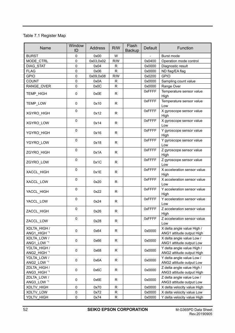
52 SEIKO EPSON CORPORATION M-G365PD Data Sheet
Rev.20190905
Table 7.1 Register Map
Name Window
ID Address R/W
Flash Backup
Default Function
BURST 0 0x00 W - Burst mode
MODE_CTRL 0 0x03,0x02 R/W 0x0400 Operation mode control
DIAG_STAT 0 0x04 R 0x0000 Diagnostic result
FLAG 0 0x06 R 0x0000 ND flag/EA flag
GPIO 0 0x09,0x08 R/W 0x0200 GPIO
COUNT 0 0x0A R 0x0000 Sampling count value
RANGE_OVER 0 0x0C R 0x0000 Range Over
TEMP_HIGH 0 0x0E R 0xFFFF Temperature sensor value
High
TEMP_LOW 0 0x10 R 0xFFFF Temperature sensor value
Low
XGYRO_HIGH 0
0x12 R 0xFFFF X gyroscope sensor value
High
XGYRO_LOW 0
0x14 R 0xFFFF X gyroscope sensor value
Low
YGYRO_HIGH 0
0x16 R 0xFFFF Y gyroscope sensor value
High
YGYRO_LOW 0
0x18 R 0xFFFF Y gyroscope sensor value
Low
ZGYRO_HIGH 0
0x1A R 0xFFFF Z gyroscope sensor value
High
ZGYRO_LOW 0
0x1C R 0xFFFF Z gyroscope sensor value
Low
XACCL_HIGH 0
0x1E R 0xFFFF X acceleration sensor value
High
XACCL_LOW 0
0x20 R 0xFFFF X acceleration sensor value
Low
YACCL_HIGH 0
0x22 R 0xFFFF Y acceleration sensor value
High
YACCL_LOW 0
0x24 R 0xFFFF Y acceleration sensor value
Low
ZACCL_HIGH 0
0x26 R 0xFFFF Z acceleration sensor value
High
ZACCL_LOW 0
0x28 R 0xFFFF Z acceleration sensor value
Low
XDLTA_HIGH /
ANG1_HIGH *1 0 0x64 R 0x0000
X delta angle value High /
ANG1 attitude output High
XDLTA_LOW /
ANG1_LOW *1 0 0x66 R 0x0000
X delta angle value Low /
ANG1 attitude output Low
YDLTA_HIGH /
ANG2_HIGH *1 0 0x68 R 0x0000
Y delta angle value High /
ANG2 attitude output High
YDLTA_LOW /
ANG2_LOW *1 0 0x6A R 0x0000
Y delta angle value Low /
ANG2 attitude output Low
ZDLTA_HIGH /
ANG3_HIGH *1 0 0x6C R 0x0000
Z delta angle value High /
ANG3 attitude output High
ZDLTA_LOW /
ANG3_LOW *1 0 0x6E R 0x0000
Z delta angle value Low /
ANG3 attitude output Low
XDLTV_HIGH 0 0x70 R 0x0000 X delta velocity value High
XDLTV_LOW 0 0x72 R 0x0000 X delta velocity value Low
YDLTV_HIGH 0 0x74 R 0x0000 Y delta velocity value High
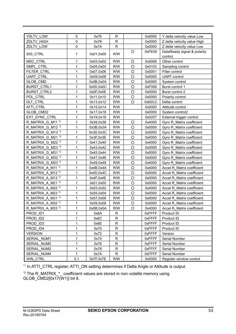
M-G365PD Data Sheet SEIKO EPSON CORPORATION 53 Rev.20190704
YDLTV_LOW 0 0x76 R 0x0000 Y delta velocity value Low
ZDLTV_HIGH 0 0x78 R 0x0000 Z delta velocity value High
ZDLTV_LOW 0 0x7A R 0x0000 Z delta velocity value Low
SIG_CTRL 1 0x01,0x00 R/W ○ 0xFE00 DataReady signal & polarity
control
MSC_CTRL 1 0x03,0x02 R/W ○ 0x0006 Other control
SMPL_CTRL 1 0x05,0x04 R/W ○ 0x0103 Sampling control
FILTER_CTRL 1 0x07,0x06 R/W ○ 0x0001 Filter control
UART_CTRL 1 0x09,0x08 R/W ○ 0x0000 UART control
GLOB_CMD 1 0x0B,0x0A R/W ○ 0x0000 System control
BURST_CTRL1 1 0x0D,0x0C R/W ○ 0xF006 Burst control 1
BURST_CTRL2 1 0x0F,0x0E R/W ○ 0x0000 Burst control 2
POL_CTRL 1 0x11,0x10 R/W ○ 0x0000 Polarity control
DLT_CTRL 1 0x13,0x12 R/W ○ 0x00CC Delta control
ATTI_CTRL 1 0x15,0x14 R/W 0x0000 Attitude control
GLOB_CMD2 1 0x17,0x16 R/W 0x0000 System control2
EXT_SYNC_CTRL 1 0x19,0x18 R/W 0x0207 External trigger control
R_MATRIX_G_M11 *2 1 0x39,0x38 R/W ○ 0x4000 Gyro R_Matrix coefficient
R_MATRIX_G_M12 *2 1 0x3B,0x3A R/W ○ 0x0000 Gyro R_Matrix coefficient
R_MATRIX_G_M13 *2 1 0x3D,0x3C R/W ○ 0x0000 Gyro R_Matrix coefficient
R_MATRIX_G_M21 *2 1 0x3F,0x3E R/W ○ 0x0000 Gyro R_Matrix coefficient
R_MATRIX_G_M22 *2 1 0x41,0x40 R/W ○ 0x4000 Gyro R_Matrix coefficient
R_MATRIX_G_M23 *2 1 0x43,0x42 R/W ○ 0x0000 Gyro R_Matrix coefficient
R_MATRIX_G_M31 *2 1 0x45,0x44 R/W ○ 0x0000 Gyro R_Matrix coefficient
R_MATRIX_G_M32 *2 1 0x47,0x46 R/W ○ 0x0000 Gyro R_Matrix coefficient
R_MATRIX_G_M33 *2 1 0x49,0x48 R/W ○ 0x4000 Gyro R_Matrix coefficient
R_MATRIX_A_M11 *2 1 0x4B,0x4A R/W ○ 0x4000 Accel R_Matrix coefficient
R_MATRIX_A_M12 *2 1 0x4D,0x4C R/W ○ 0x0000 Accel R_Matrix coefficient
R_MATRIX_A_M13 *2 1 0x4F,0x4E R/W ○ 0x0000 Accel R_Matrix coefficient
R_MATRIX_A_M21 *2 1 0x51,0x50 R/W ○ 0x0000 Accel R_Matrix coefficient
R_MATRIX_A_M22 *2 1 0x53,0x52 R/W ○ 0x4000 Accel R_Matrix coefficient
R_MATRIX_A_M23 *2 1 0x55,0x54 R/W ○ 0x0000 Accel R_Matrix coefficient
R_MATRIX_A_M31 *2 1 0x57,0x56 R/W ○ 0x0000 Accel R_Matrix coefficient
R_MATRIX_A_M32 *2 1 0x59,0x58 R/W ○ 0x0000 Accel R_Matrix coefficient
R_MATRIX_A_M33 *2 1 0x5B,0x5A R/W ○ 0x4000 Accel R_Matrix coefficient
PROD_ID1 1 0x6A R 0xFFFF Product ID
PROD_ID2 1 0x6C R 0xFFFF Product ID
PROD_ID3 1 0x6E R 0xFFFF Product ID
PROD_ID4 1 0x70 R 0xFFFF Product ID
VERSION 1 0x72 R 0xFFFF Version
SERIAL_NUM1 1 0x74 R 0xFFFF Serial Number
SERIAL_NUM2 1 0x76 R 0xFFFF Serial Number
SERIAL_NUM3 1 0x78 R 0xFFFF Serial Number
SERIAL_NUM4 1 0x7A R 0xFFFF Serial Number
WIN_CTRL 0,1 0x7F,0x7E R/W 0x0000 Register window control
*1 In ATTI_CTRL register, ATTI_ON setting determines if Delta Angle or Attitude is output.
*2 The R_MATRIX_*_ coefficient values are stored in non-volatile memory using GLOB_CMD2[0x17(W1)] bit 8.
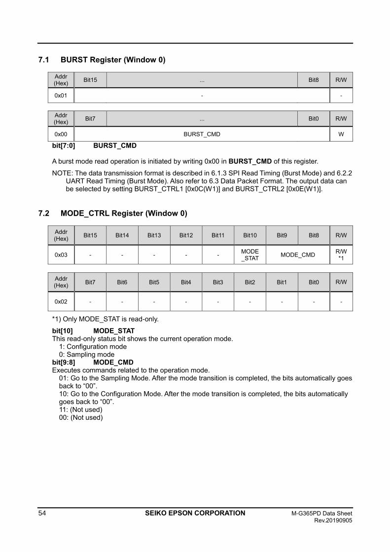
54 SEIKO EPSON CORPORATION M-G365PD Data Sheet
Rev.20190905
7.1 BURST Register (Window 0)
Addr (Hex)
Bit15 ... Bit8 R/W
0x01 - -
Addr (Hex)
Bit7 ... Bit0 R/W
0x00 BURST_CMD W
bit[7:0] BURST_CMD A burst mode read operation is initiated by writing 0x00 in BURST_CMD of this register.
NOTE: The data transmission format is described in 6.1.3 SPI Read Timing (Burst Mode) and 6.2.2 UART Read Timing (Burst Mode). Also refer to 6.3 Data Packet Format. The output data can be selected by setting BURST_CTRL1 [0x0C(W1)] and BURST_CTRL2 [0x0E(W1)].
7.2 MODE_CTRL Register (Window 0)
Addr (Hex)
Bit15 Bit14 Bit13 Bit12 Bit11 Bit10 Bit9 Bit8 R/W
0x03 - - - - - MODE _STAT
MODE_CMD R/W *1
Addr (Hex)
Bit7 Bit6 Bit5 Bit4 Bit3 Bit2 Bit1 Bit0 R/W
0x02 - - - - - - - - -
*1) Only MODE_STAT is read-only.
bit[10] MODE_STAT This read-only status bit shows the current operation mode.
1: Configuration mode 0: Sampling mode
bit[9:8] MODE_CMD Executes commands related to the operation mode.
01: Go to the Sampling Mode. After the mode transition is completed, the bits automatically goes back to “00”. 10: Go to the Configuration Mode. After the mode transition is completed, the bits automatically goes back to “00”. 11: (Not used) 00: (Not used)
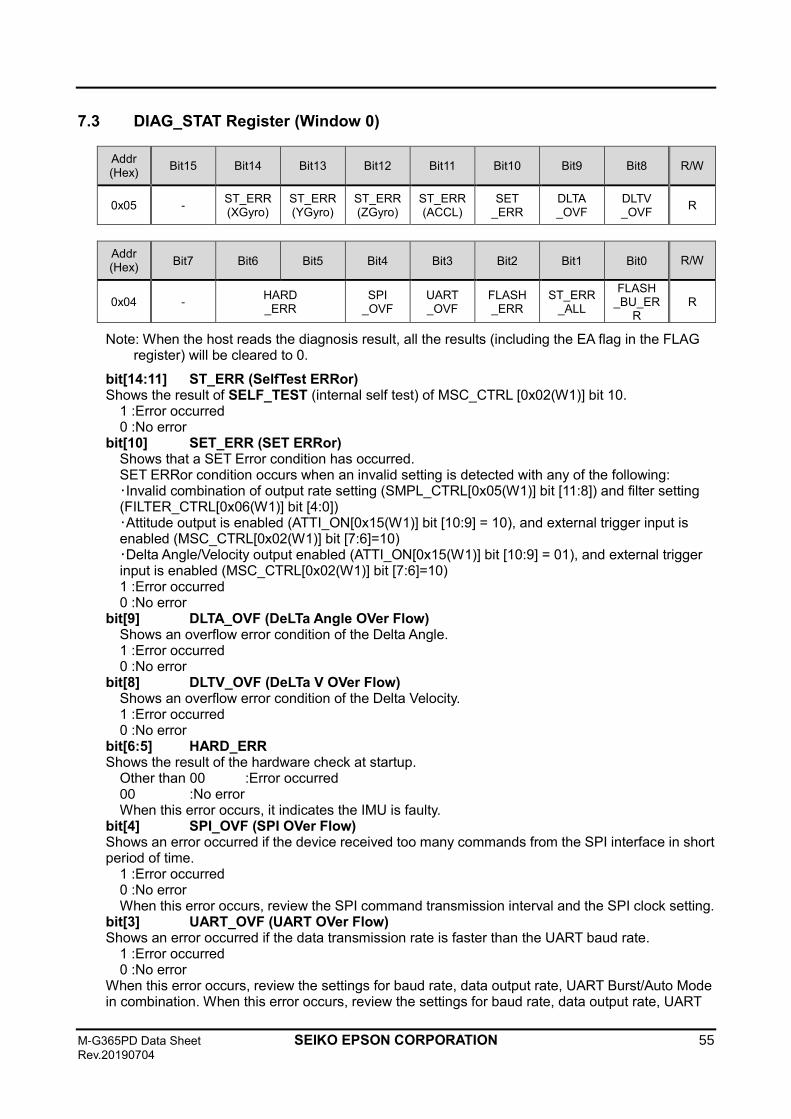
M-G365PD Data Sheet SEIKO EPSON CORPORATION 55 Rev.20190704
7.3 DIAG_STAT Register (Window 0)
Addr (Hex)
Bit15 Bit14 Bit13 Bit12 Bit11 Bit10 Bit9 Bit8 R/W
0x05 - ST_ERR (XGyro)
ST_ERR (YGyro)
ST_ERR (ZGyro)
ST_ERR (ACCL)
SET _ERR
DLTA _OVF
DLTV _OVF
R
Addr (Hex)
Bit7 Bit6 Bit5 Bit4 Bit3 Bit2 Bit1 Bit0 R/W
0x04 - HARD _ERR
SPI _OVF
UART _OVF
FLASH _ERR
ST_ERR _ALL
FLASH _BU_ER
R R
Note: When the host reads the diagnosis result, all the results (including the EA flag in the FLAG register) will be cleared to 0.
bit[14:11] ST_ERR (SelfTest ERRor) Shows the result of SELF_TEST (internal self test) of MSC_CTRL [0x02(W1)] bit 10.
1 :Error occurred 0 :No error
bit[10] SET_ERR (SET ERRor) Shows that a SET Error condition has occurred. SET ERRor condition occurs when an invalid setting is detected with any of the following: ・Invalid combination of output rate setting (SMPL_CTRL[0x05(W1)] bit [11:8]) and filter setting (FILTER_CTRL[0x06(W1)] bit [4:0]) ・Attitude output is enabled (ATTI_ON[0x15(W1)] bit [10:9] = 10), and external trigger input is enabled (MSC_CTRL[0x02(W1)] bit [7:6]=10) ・Delta Angle/Velocity output enabled (ATTI_ON[0x15(W1)] bit [10:9] = 01), and external trigger input is enabled (MSC_CTRL[0x02(W1)] bit [7:6]=10) 1 :Error occurred 0 :No error
bit[9] DLTA_OVF (DeLTa Angle OVer Flow) Shows an overflow error condition of the Delta Angle. 1 :Error occurred 0 :No error
bit[8] DLTV_OVF (DeLTa V OVer Flow) Shows an overflow error condition of the Delta Velocity. 1 :Error occurred 0 :No error
bit[6:5] HARD_ERR Shows the result of the hardware check at startup.
Other than 00 :Error occurred 00 :No error When this error occurs, it indicates the IMU is faulty.
bit[4] SPI_OVF (SPI OVer Flow) Shows an error occurred if the device received too many commands from the SPI interface in short period of time.
1 :Error occurred 0 :No error When this error occurs, review the SPI command transmission interval and the SPI clock setting.
bit[3] UART_OVF (UART OVer Flow) Shows an error occurred if the data transmission rate is faster than the UART baud rate.
1 :Error occurred 0 :No error
When this error occurs, review the settings for baud rate, data output rate, UART Burst/Auto Mode in combination. When this error occurs, review the settings for baud rate, data output rate, UART
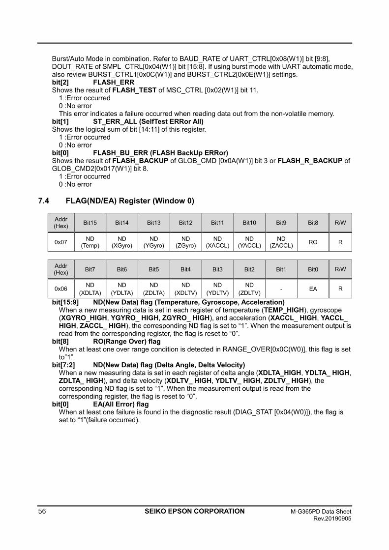
56 SEIKO EPSON CORPORATION M-G365PD Data Sheet
Rev.20190905
Burst/Auto Mode in combination. Refer to BAUD_RATE of UART_CTRL[0x08(W1)] bit [9:8], DOUT_RATE of SMPL_CTRL[0x04(W1)] bit [15:8]. If using burst mode with UART automatic mode, also review BURST_CTRL1[0x0C(W1)] and BURST_CTRL2[0x0E(W1)] settings. bit[2] FLASH_ERR Shows the result of FLASH_TEST of MSC_CTRL [0x02(W1)] bit 11.
1 :Error occurred 0 :No error This error indicates a failure occurred when reading data out from the non-volatile memory.
bit[1] ST_ERR_ALL (SelfTest ERRor All) Shows the logical sum of bit [14:11] of this register.
1 :Error occurred 0 :No error
bit[0] FLASH_BU_ERR (FLASH BackUp ERRor) Shows the result of FLASH_BACKUP of GLOB_CMD [0x0A(W1)] bit 3 or FLASH_R_BACKUP of GLOB_CMD2[0x017(W1)] bit 8.
1 :Error occurred 0 :No error
7.4 FLAG(ND/EA) Register (Window 0)
Addr (Hex)
Bit15 Bit14 Bit13 Bit12 Bit11 Bit10 Bit9 Bit8 R/W
0x07 ND
(Temp) ND
(XGyro) ND
(YGyro) ND
(ZGyro) ND
(XACCL) ND
(YACCL) ND
(ZACCL) RO R
Addr (Hex)
Bit7 Bit6 Bit5 Bit4 Bit3 Bit2 Bit1 Bit0 R/W
0x06 ND
(XDLTA)
ND
(YDLTA)
ND
(ZDLTA)
ND
(XDLTV)
ND
(YDLTV)
ND
(ZDLTV) - EA R
bit[15:9] ND(New Data) flag (Temperature, Gyroscope, Acceleration) When a new measuring data is set in each register of temperature (TEMP_HIGH), gyroscope (XGYRO_HIGH, YGYRO_ HIGH, ZGYRO_ HIGH), and acceleration (XACCL_ HIGH, YACCL_ HIGH, ZACCL_ HIGH), the corresponding ND flag is set to “1”. When the measurement output is read from the corresponding register, the flag is reset to “0”.
bit[8] RO(Range Over) flag When at least one over range condition is detected in RANGE_OVER[0x0C(W0)], this flag is set to”1”.
bit[7:2] ND(New Data) flag (Delta Angle, Delta Velocity) When a new measuring data is set in each register of delta angle (XDLTA_HIGH, YDLTA_ HIGH, ZDLTA_ HIGH), and delta velocity (XDLTV_ HIGH, YDLTV_ HIGH, ZDLTV_ HIGH), the corresponding ND flag is set to “1”. When the measurement output is read from the corresponding register, the flag is reset to “0”.
bit[0] EA(All Error) flag When at least one failure is found in the diagnostic result (DIAG_STAT [0x04(W0)]), the flag is set to “1”(failure occurred).
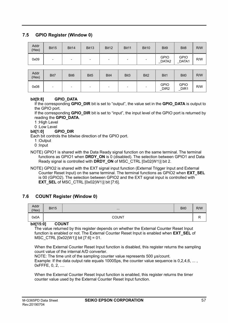
M-G365PD Data Sheet SEIKO EPSON CORPORATION 57 Rev.20190704
7.5 GPIO Register (Window 0)
Addr (Hex)
Bit15 Bit14 Bit13 Bit12 Bit11 Bit10 Bit9 Bit8 R/W
0x09 - - - - - - GPIO
_DATA2 GPIO
_DATA1 R/W
Addr (Hex)
Bit7 Bit6 Bit5 Bit4 Bit3 Bit2 Bit1 Bit0 R/W
0x08 - - - - - - GPIO _DIR2
GPIO _DIR1
R/W
bit[9:8] GPIO_DATA
If the corresponding GPIO_DIR bit is set to “output”, the value set in the GPIO_DATA is output to the GPIO port. If the corresponding GPIO_DIR bit is set to “input”, the input level of the GPIO port is returned by reading the GPIO_DATA. 1 :High Level 0 :Low Level
bit[1:0] GPIO_DIR Each bit controls the bitwise direction of the GPIO port.
1 :Output 0 :Input
NOTE) GPIO1 is shared with the Data Ready signal function on the same terminal. The terminal functions as GPIO1 when DRDY_ON is 0 (disabled). The selection between GPIO1 and Data Ready signal is controlled with DRDY_ON of MSC_CTRL [0x02(W1)] bit 2.
NOTE) GPIO2 is shared with the EXT signal input function (External Trigger Input and External Counter Reset Input) on the same terminal. The terminal functions as GPIO2 when EXT_SEL is 00 (GPIO2). The selection between GPIO2 and the EXT signal input is controlled with EXT_SEL of MSC_CTRL [0x02(W1)] bit [7:6].
7.6 COUNT Register (Window 0)
Addr (Hex)
Bit15 ... Bit0 R/W
0x0A COUNT R
bit[15:0] COUNT The value returned by this register depends on whether the External Counter Reset Input function is enabled or not. The External Counter Reset Input is enabled when EXT_SEL of MSC_CTRL [0x02(W1)] bit [7:6] = 01. When the External Counter Reset Input function is disabled, this register returns the sampling count value of the internal A/D converter. NOTE: The time unit of the sampling counter value represents 500 μs/count. Example: If the data output rate equals 1000Sps, the counter value sequence is 0,2,4,6, ... , 0xFFFE, 0, 2, .... When the External Counter Reset Input function is enabled, this register returns the timer counter value used by the External Counter Reset Input function.
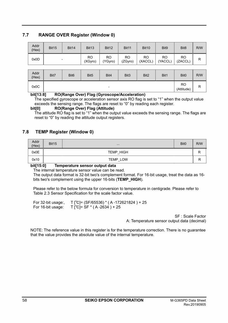
58 SEIKO EPSON CORPORATION M-G365PD Data Sheet
Rev.20190905
7.7 RANGE OVER Register (Window 0)
Addr (Hex)
Bit15 Bit14 Bit13 Bit12 Bit11 Bit10 Bit9 Bit8 R/W
0x0D - RO
(XGyro) RO
(YGyro) RO
(ZGyro) RO
(XACCL) RO
(YACCL) RO
(ZACCL) R
Addr (Hex)
Bit7 Bit6 Bit5 Bit4 Bit3 Bit2 Bit1 Bit0 R/W
0x0C - RO
(Attitude) R
bit[13:8] RO(Range Over) Flag (Gyroscope/Acceleration) The specified gyroscope or acceleration sensor axis RO flag is set to “1” when the output value exceeds the sensing range. The flags are reset to “0” by reading each register.
bit[0] RO(Range Over) Flag (Attitude) The attitude RO flag is set to “1” when the output value exceeds the sensing range. The flags are reset to “0” by reading the attitude output registers.
7.8 TEMP Register (Window 0)
Addr (Hex)
Bit15 ... Bit0 R/W
0x0E TEMP_HIGH R
0x10 TEMP_LOW R
bit[15:0] Temperature sensor output data The internal temperature sensor value can be read. The output data format is 32-bit two's complement format. For 16-bit usage, treat the data as 16- bits two's complement using the upper 16-bits (TEMP_HIGH).
Please refer to the below formula for conversion to temperature in centigrade. Please refer to Table 2.3 Sensor Specification for the scale factor value. For 32-bit usage:, T [℃]= (SF/65536) * ( A -172621824 ) + 25 For 16-bit usage: T [℃]= SF * ( A -2634 ) + 25
SF : Scale Factor
A: Temperature sensor output data (decimal) NOTE: The reference value in this register is for the temperature correction. There is no guarantee that the value provides the absolute value of the internal temperature.
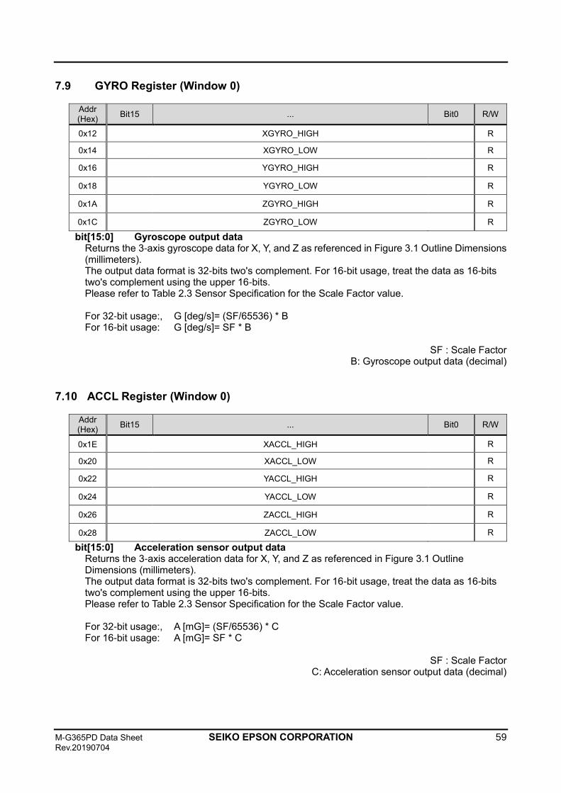
M-G365PD Data Sheet SEIKO EPSON CORPORATION 59 Rev.20190704
7.9 GYRO Register (Window 0)
Addr (Hex)
Bit15 ... Bit0 R/W
0x12 XGYRO_HIGH R
0x14 XGYRO_LOW R
0x16 YGYRO_HIGH R
0x18 YGYRO_LOW R
0x1A ZGYRO_HIGH R
0x1C ZGYRO_LOW R
bit[15:0] Gyroscope output data Returns the 3-axis gyroscope data for X, Y, and Z as referenced in Figure 3.1 Outline Dimensions (millimeters). The output data format is 32-bits two's complement. For 16-bit usage, treat the data as 16-bits two's complement using the upper 16-bits. Please refer to Table 2.3 Sensor Specification for the Scale Factor value. For 32-bit usage:, G [deg/s]= (SF/65536) * B For 16-bit usage: G [deg/s]= SF * B
SF : Scale Factor B: Gyroscope output data (decimal)
7.10 ACCL Register (Window 0)
Addr (Hex)
Bit15 ... Bit0 R/W
0x1E XACCL_HIGH R
0x20 XACCL_LOW R
0x22 YACCL_HIGH R
0x24 YACCL_LOW R
0x26 ZACCL_HIGH R
0x28 ZACCL_LOW R
bit[15:0] Acceleration sensor output data Returns the 3-axis acceleration data for X, Y, and Z as referenced in Figure 3.1 Outline Dimensions (millimeters). The output data format is 32-bits two's complement. For 16-bit usage, treat the data as 16-bits two's complement using the upper 16-bits. Please refer to Table 2.3 Sensor Specification for the Scale Factor value. For 32-bit usage:, A [mG]= (SF/65536) * C For 16-bit usage: A [mG]= SF * C
SF : Scale Factor C: Acceleration sensor output data (decimal)
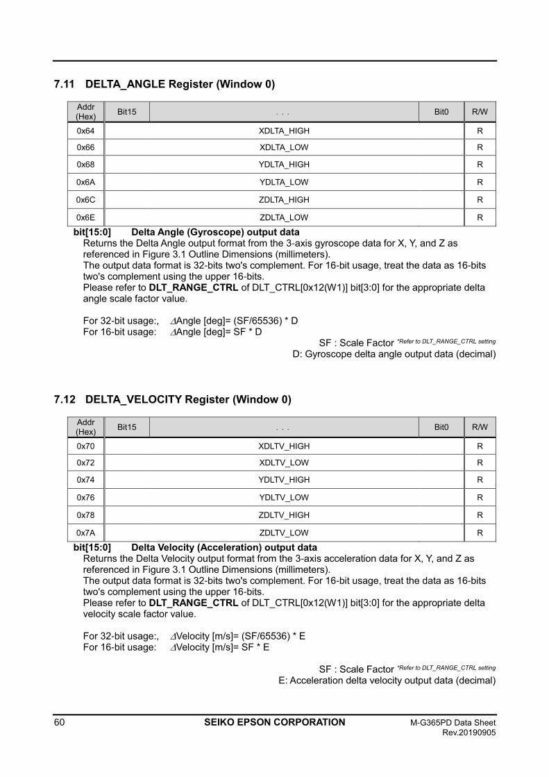
60 SEIKO EPSON CORPORATION M-G365PD Data Sheet
Rev.20190905
7.11 DELTA_ANGLE Register (Window 0)
Addr (Hex)
Bit15 ... Bit0 R/W
0x64 XDLTA_HIGH R
0x66 XDLTA_LOW R
0x68 YDLTA_HIGH R
0x6A YDLTA_LOW R
0x6C ZDLTA_HIGH R
0x6E ZDLTA_LOW R
bit[15:0] Delta Angle (Gyroscope) output data Returns the Delta Angle output format from the 3-axis gyroscope data for X, Y, and Z as referenced in Figure 3.1 Outline Dimensions (millimeters). The output data format is 32-bits two's complement. For 16-bit usage, treat the data as 16-bits two's complement using the upper 16-bits. Please refer to DLT_RANGE_CTRL of DLT_CTRL[0x12(W1)] bit[3:0] for the appropriate delta angle scale factor value. For 32-bit usage:, Angle [deg]= (SF/65536) * D For 16-bit usage: Angle [deg]= SF * D
SF : Scale Factor *Refer to DLT_RANGE_CTRL setting D: Gyroscope delta angle output data (decimal)
7.12 DELTA_VELOCITY Register (Window 0)
Addr (Hex)
Bit15 ... Bit0 R/W
0x70 XDLTV_HIGH R
0x72 XDLTV_LOW R
0x74 YDLTV_HIGH R
0x76 YDLTV_LOW R
0x78 ZDLTV_HIGH R
0x7A ZDLTV_LOW R
bit[15:0] Delta Velocity (Acceleration) output data Returns the Delta Velocity output format from the 3-axis acceleration data for X, Y, and Z as referenced in Figure 3.1 Outline Dimensions (millimeters). The output data format is 32-bits two's complement. For 16-bit usage, treat the data as 16-bits two's complement using the upper 16-bits. Please refer to DLT_RANGE_CTRL of DLT_CTRL[0x12(W1)] bit[3:0] for the appropriate delta velocity scale factor value. For 32-bit usage:, Velocity [m/s]= (SF/65536) * E For 16-bit usage: Velocity [m/s]= SF * E
SF : Scale Factor *Refer to DLT_RANGE_CTRL setting E: Acceleration delta velocity output data (decimal)
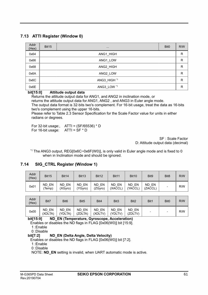
M-G365PD Data Sheet SEIKO EPSON CORPORATION 61 Rev.20190704
7.13 ATTI Register (Window 0)
Addr (Hex)
Bit15 ... Bit0 R/W
0x64 ANG1_HIGH R
0x66 ANG1_LOW R
0x68 ANG2_HIGH R
0x6A ANG2_LOW R
0x6C ANG3_HIGH *1 R
0x6E ANG3_LOW *1 R
bit[15:0] Attitude output data Returns the attitude output data for ANG1, and ANG2 in inclination mode, or returns the attitude output data for ANG1, ANG2 , and ANG3 in Euler angle mode. The output data format is 32-bits two's complement. For 16-bit usage, treat the data as 16-bits two's complement using the upper 16-bits. Please refer to Table 2.3 Sensor Specification for the Scale Factor value for units in either radians or degrees. For 32-bit usage:, ATTI = (SF/65536) * D For 16-bit usage: ATTI = SF * D
SF : Scale Factor D: Attitude output data (decimal)
*1 The ANG3 output, REG[0x6C~0x6F(W0)], is only valid in Euler angle mode and is fixed to 0
when in Inclination mode and should be ignored.
7.14 SIG_CTRL Register (Window 1)
Addr (Hex)
Bit15 Bit14 Bit13 Bit12 Bit11 Bit10 Bit9 Bit8 R/W
0x01 ND_EN (Temp)
ND_EN (XGyro)
ND_EN (YGyro)
ND_EN (ZGyro)
ND_EN (XACCL)
ND_EN (YACCL)
ND_EN (ZACCL)
- R/W
Addr (Hex)
Bit7 Bit6 Bit5 Bit4 Bit3 Bit2 Bit1 Bit0 R/W
0x00 ND_EN
(XDLTA)
ND_EN
(YDLTA)
ND_EN
(ZDLTA)
ND_EN
(XDLTV)
ND_EN
(YDLTV)
ND_EN
(ZDLTV) - - R/W
bit[15:9] ND_EN (Temperature, Gyroscope, Acceleration) Enables or disables the ND flags in FLAG [0x06(W0)] bit [15:9]. 1 :Enable 0 :Disable
bit[7:2] ND_EN (Delta Angle, Delta Velocity) Enables or disables the ND flags in FLAG [0x06(W0)] bit [7:2]. 1 :Enable 0 :Disable NOTE: ND_EN setting is invalid, when UART automatic mode is active.
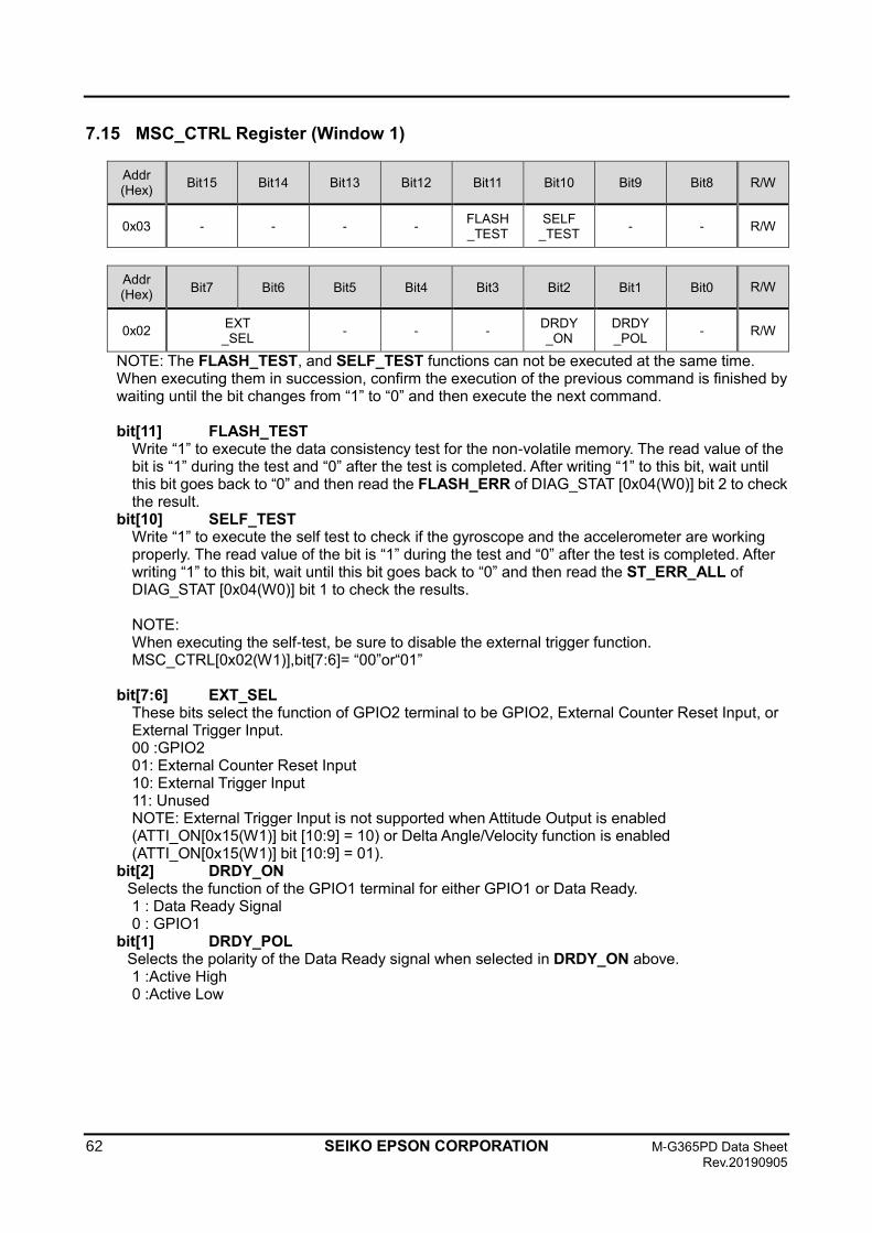
62 SEIKO EPSON CORPORATION M-G365PD Data Sheet
Rev.20190905
7.15 MSC_CTRL Register (Window 1)
Addr (Hex)
Bit15 Bit14 Bit13 Bit12 Bit11 Bit10 Bit9 Bit8 R/W
0x03 - - - - FLASH _TEST
SELF _TEST
- - R/W
Addr (Hex)
Bit7 Bit6 Bit5 Bit4 Bit3 Bit2 Bit1 Bit0 R/W
0x02 EXT _SEL
- - - DRDY _ON
DRDY _POL
- R/W
NOTE: The FLASH_TEST, and SELF_TEST functions can not be executed at the same time. When executing them in succession, confirm the execution of the previous command is finished by waiting until the bit changes from “1” to “0” and then execute the next command. bit[11] FLASH_TEST
Write “1” to execute the data consistency test for the non-volatile memory. The read value of the bit is “1” during the test and “0” after the test is completed. After writing “1” to this bit, wait until this bit goes back to “0” and then read the FLASH_ERR of DIAG_STAT [0x04(W0)] bit 2 to check the result.
bit[10] SELF_TEST Write “1” to execute the self test to check if the gyroscope and the accelerometer are working properly. The read value of the bit is “1” during the test and “0” after the test is completed. After writing “1” to this bit, wait until this bit goes back to “0” and then read the ST_ERR_ALL of DIAG_STAT [0x04(W0)] bit 1 to check the results. NOTE: When executing the self-test, be sure to disable the external trigger function. MSC_CTRL[0x02(W1)],bit[7:6]= “00”or“01”
bit[7:6] EXT_SEL These bits select the function of GPIO2 terminal to be GPIO2, External Counter Reset Input, or External Trigger Input. 00 :GPIO2 01: External Counter Reset Input 10: External Trigger Input 11: Unused NOTE: External Trigger Input is not supported when Attitude Output is enabled (ATTI_ON[0x15(W1)] bit [10:9] = 10) or Delta Angle/Velocity function is enabled (ATTI_ON[0x15(W1)] bit [10:9] = 01).
bit[2] DRDY_ON Selects the function of the GPIO1 terminal for either GPIO1 or Data Ready. 1 : Data Ready Signal 0 : GPIO1
bit[1] DRDY_POL Selects the polarity of the Data Ready signal when selected in DRDY_ON above. 1 :Active High 0 :Active Low
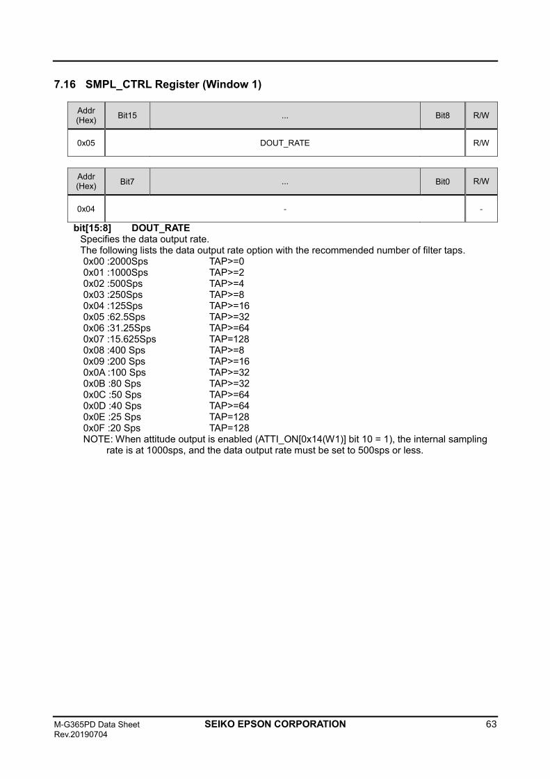
M-G365PD Data Sheet SEIKO EPSON CORPORATION 63 Rev.20190704
7.16 SMPL_CTRL Register (Window 1)
Addr (Hex)
Bit15 ... Bit8 R/W
0x05 DOUT_RATE R/W
Addr (Hex)
Bit7 ... Bit0 R/W
0x04 - -
bit[15:8] DOUT_RATE Specifies the data output rate. The following lists the data output rate option with the recommended number of filter taps. 0x00 :2000Sps TAP>=0 0x01 :1000Sps TAP>=2 0x02 :500Sps TAP>=4 0x03 :250Sps TAP>=8 0x04 :125Sps TAP>=16 0x05 :62.5Sps TAP>=32 0x06 :31.25Sps TAP>=64 0x07 :15.625Sps TAP=128 0x08 :400 Sps TAP>=8 0x09 :200 Sps TAP>=16 0x0A :100 Sps TAP>=32 0x0B :80 Sps TAP>=32 0x0C :50 Sps TAP>=64 0x0D :40 Sps TAP>=64 0x0E :25 Sps TAP=128 0x0F :20 Sps TAP=128 NOTE: When attitude output is enabled (ATTI_ON[0x14(W1)] bit 10 = 1), the internal sampling
rate is at 1000sps, and the data output rate must be set to 500sps or less.
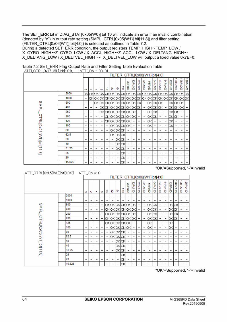
64 SEIKO EPSON CORPORATION M-G365PD Data Sheet
Rev.20190905
The SET_ERR bit in DIAG_STAT[0x05(W0)] bit 10 will indicate an error if an invalid combination (denoted by “x”) in output rate setting (SMPL_CTRL[0x05(W1)] bit[11:8]) and filter setting (FILTER_CTRL[0x06(W1)] bit[4:0]) is selected as outlined in Table 7.2. During a detected SET_ERR condition, the output registers TEMP_HIGH~TEMP_LOW / X_GYRO_HIGH~Z_GYRO_LOW / X_ACCL_HIGH~Z_ACCL_LOW / X_DELTANG_HIGH~X_DELTANG_LOW / X_DELTVEL_HIGH ~ X_DELTVEL_LOW will output a fixed value 0x7EF0.
Table 7.2 SET_ERR Flag Output Rate and Filter Setting Table Evaluation Table
“OK”=Supported, “-”=Invalid
“OK”=Supported, “-”=Invalid
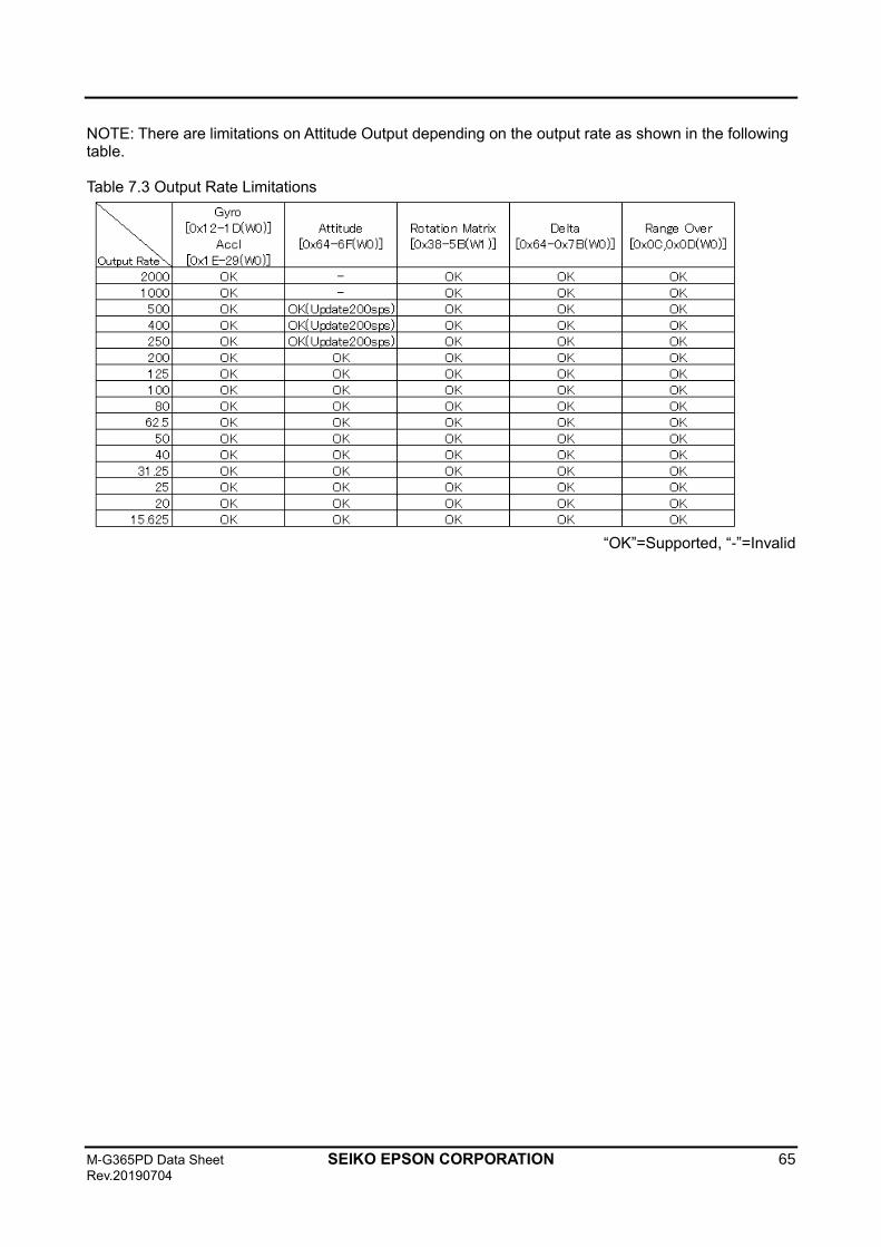
M-G365PD Data Sheet SEIKO EPSON CORPORATION 65 Rev.20190704
NOTE: There are limitations on Attitude Output depending on the output rate as shown in the following table. Table 7.3 Output Rate Limitations
“OK”=Supported, “-”=Invalid
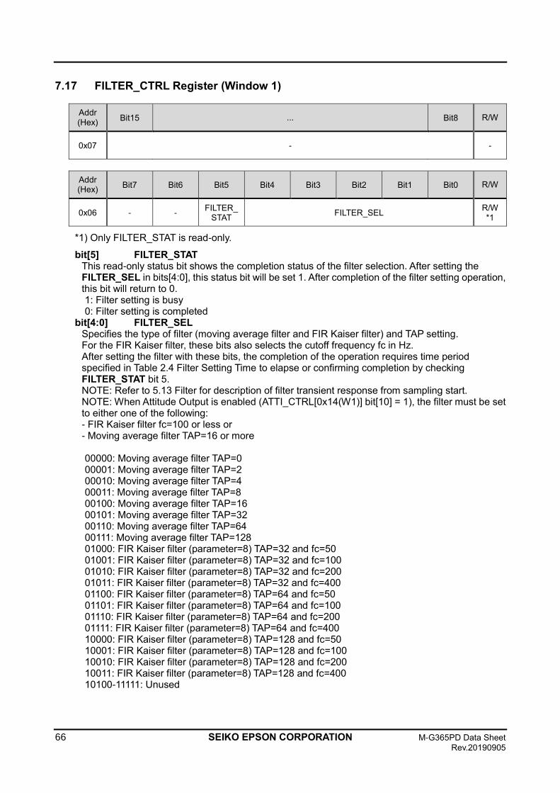
66 SEIKO EPSON CORPORATION M-G365PD Data Sheet
Rev.20190905
7.17 FILTER_CTRL Register (Window 1)
Addr (Hex)
Bit15 ... Bit8 R/W
0x07 - -
Addr (Hex)
Bit7 Bit6 Bit5 Bit4 Bit3 Bit2 Bit1 Bit0 R/W
0x06 - - FILTER_
STAT FILTER_SEL
R/W *1
*1) Only FILTER_STAT is read-only.
bit[5] FILTER_STAT This read-only status bit shows the completion status of the filter selection. After setting the FILTER_SEL in bits[4:0], this status bit will be set 1. After completion of the filter setting operation, this bit will return to 0. 1: Filter setting is busy 0: Filter setting is completed
bit[4:0] FILTER_SEL Specifies the type of filter (moving average filter and FIR Kaiser filter) and TAP setting. For the FIR Kaiser filter, these bits also selects the cutoff frequency fc in Hz. After setting the filter with these bits, the completion of the operation requires time period specified in Table 2.4 Filter Setting Time to elapse or confirming completion by checking FILTER_STAT bit 5. NOTE: Refer to 5.13 Filter for description of filter transient response from sampling start. NOTE: When Attitude Output is enabled (ATTI_CTRL[0x14(W1)] bit[10] = 1), the filter must be set to either one of the following: - FIR Kaiser filter fc=100 or less or - Moving average filter TAP=16 or more 00000: Moving average filter TAP=0 00001: Moving average filter TAP=2 00010: Moving average filter TAP=4 00011: Moving average filter TAP=8 00100: Moving average filter TAP=16 00101: Moving average filter TAP=32 00110: Moving average filter TAP=64 00111: Moving average filter TAP=128 01000: FIR Kaiser filter (parameter=8) TAP=32 and fc=50 01001: FIR Kaiser filter (parameter=8) TAP=32 and fc=100 01010: FIR Kaiser filter (parameter=8) TAP=32 and fc=200 01011: FIR Kaiser filter (parameter=8) TAP=32 and fc=400 01100: FIR Kaiser filter (parameter=8) TAP=64 and fc=50 01101: FIR Kaiser filter (parameter=8) TAP=64 and fc=100 01110: FIR Kaiser filter (parameter=8) TAP=64 and fc=200 01111: FIR Kaiser filter (parameter=8) TAP=64 and fc=400 10000: FIR Kaiser filter (parameter=8) TAP=128 and fc=50 10001: FIR Kaiser filter (parameter=8) TAP=128 and fc=100 10010: FIR Kaiser filter (parameter=8) TAP=128 and fc=200 10011: FIR Kaiser filter (parameter=8) TAP=128 and fc=400 10100-11111: Unused
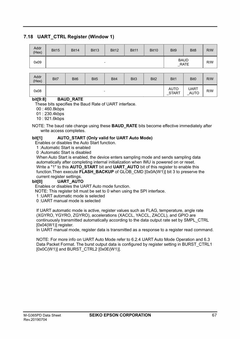
M-G365PD Data Sheet SEIKO EPSON CORPORATION 67 Rev.20190704
7.18 UART_CTRL Register (Window 1)
Addr (Hex)
Bit15 Bit14 Bit13 Bit12 Bit11 Bit10 Bit9 Bit8 R/W
0x09 - BAUD _RATE
R/W
Addr (Hex)
Bit7 Bit6 Bit5 Bit4 Bit3 Bit2 Bit1 Bit0 R/W
0x08 - AUTO
_START UART
_AUTO R/W
bit[9:8] BAUD_RATE These bits specifies the Baud Rate of UART interface. 00 : 460.8kbps 01 : 230.4kbps 10 : 921.6kbps
NOTE: The baud rate change using these BAUD_RATE bits become effective immediately after write access completes.
bit[1] AUTO_START (Only valid for UART Auto Mode) Enables or disables the Auto Start function. 1 :Automatic Start is enabled 0 :Automatic Start is disabled When Auto Start is enabled, the device enters sampling mode and sends sampling data automatically after completing internal initialization when IMU is powered on or reset. Write a "1" to this AUTO_START bit and UART_AUTO bit of this register to enable this function.Then execute FLASH_BACKUP of GLOB_CMD [0x0A(W1)] bit 3 to preserve the current register settings.
bit[0] UART_AUTO Enables or disables the UART Auto mode function. NOTE: This register bit must be set to 0 when using the SPI interface. 1 :UART automatic mode is selected 0 :UART manual mode is selected
If UART automatic mode is active, register values such as FLAG, temperature, angle rate (XGYRO, YGYRO, ZGYRO), accelerations (XACCL, YACCL, ZACCL), and GPIO are continuously transmitted automatically according to the data output rate set by SMPL_CTRL [0x04(W1)] register. In UART manual mode, register data is transmitted as a response to a register read command. NOTE: For more info on UART Auto Mode refer to 6.2.4 UART Auto Mode Operation and 6.3 Data Packet Format. The burst output data is configured by register setting in BURST_CTRL1 [0x0C(W1)] and BURST_CTRL2 [0x0E(W1)].
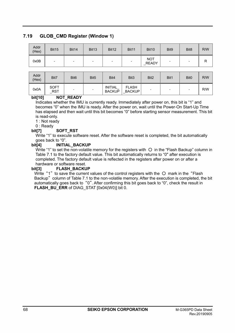
68 SEIKO EPSON CORPORATION M-G365PD Data Sheet
Rev.20190905
7.19 GLOB_CMD Register (Window 1)
Addr (Hex)
Bit15 Bit14 Bit13 Bit12 Bit11 Bit10 Bit9 Bit8 R/W
0x0B - - - - - NOT
_READY - - R
Addr (Hex)
Bit7 Bit6 Bit5 Bit4 Bit3 Bit2 Bit1 Bit0 R/W
0x0A SOFT _RST
- - INITIAL_BACKUP
FLASH _BACKUP
- - - R/W
bit[10] NOT_READY Indicates whether the IMU is currently ready. Immediately after power on, this bit is “1” and becomes “0” when the IMU is ready. After the power on, wait until the Power-On Start-Up Time has elapsed and then wait until this bit becomes “0” before starting sensor measurement. This bit is read-only. 1 : Not ready 0 : Ready
bit[7] SOFT_RST Write “1” to execute software reset. After the software reset is completed, the bit automatically goes back to “0”.
bit[4] INITIAL_BACKUP Write “1” to set the non-volatile memory for the registers with ○ in the “Flash Backup” column in Table 7.1 to the factory default value. This bit automatically returns to “0" after execution is completed. The factory default value is reflected in the registers after power on or after a hardware or software reset.
bit[3] FLASH_BACKUP Write “1” to save the current values of the control registers with the ○ mark in the “Flash Backup” column of Table 7.1 to the non-volatile memory. After the execution is completed, the bit automatically goes back to “0”. After confirming this bit goes back to “0”, check the result in FLASH_BU_ERR of DIAG_STAT [0x04(W0)] bit 0.
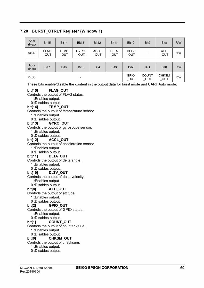
M-G365PD Data Sheet SEIKO EPSON CORPORATION 69 Rev.20190704
7.20 BURST_CTRL1 Register (Window 1)
Addr (Hex)
Bit15 Bit14 Bit13 Bit12 Bit11 Bit10 Bit9 Bit8 R/W
0x0D FLAG _OUT
TEMP _OUT
GYRO _OUT
ACCL _OUT
DLTA _OUT
DLTV _OUT
- ATTI
_OUT R/W
Addr (Hex)
Bit7 Bit6 Bit5 Bit4 Bit3 Bit2 Bit1 Bit0 R/W
0x0C - GPIO _OUT
COUNT _OUT
CHKSM _OUT
R/W
These bits enable/disable the content in the output data for burst mode and UART Auto mode.
bit[15] FLAG_OUT Controls the output of FLAG status.
1 :Enables output. 0 :Disables output.
bit[14] TEMP_OUT Controls the output of temperature sensor.
1 :Enables output. 0 :Disables output.
bit[13] GYRO_OUT Controls the output of gyroscope sensor.
1 :Enables output. 0 :Disables output.
bit[12] ACCL_OUT Controls the output of acceleration sensor.
1 :Enables output. 0 :Disables output.
bit[11] DLTA_OUT Controls the output of delta angle.
1 :Enables output. 0 :Disables output.
bit[10] DLTV_OUT Controls the output of delta velocity.
1 :Enables output. 0 :Disables output.
bit[8] ATTI_OUT Controls the output of attitude.
1 :Enables output. 0 :Disables output.
bit[2] GPIO_OUT Controls the output of GPIO status.
1 :Enables output. 0 :Disables output.
bit[1] COUNT_OUT Controls the output of counter value.
1 :Enables output. 0 :Disables output.
bit[0] CHKSM_OUT Controls the output of checksum.
1 :Enables output. 0 :Disables output.
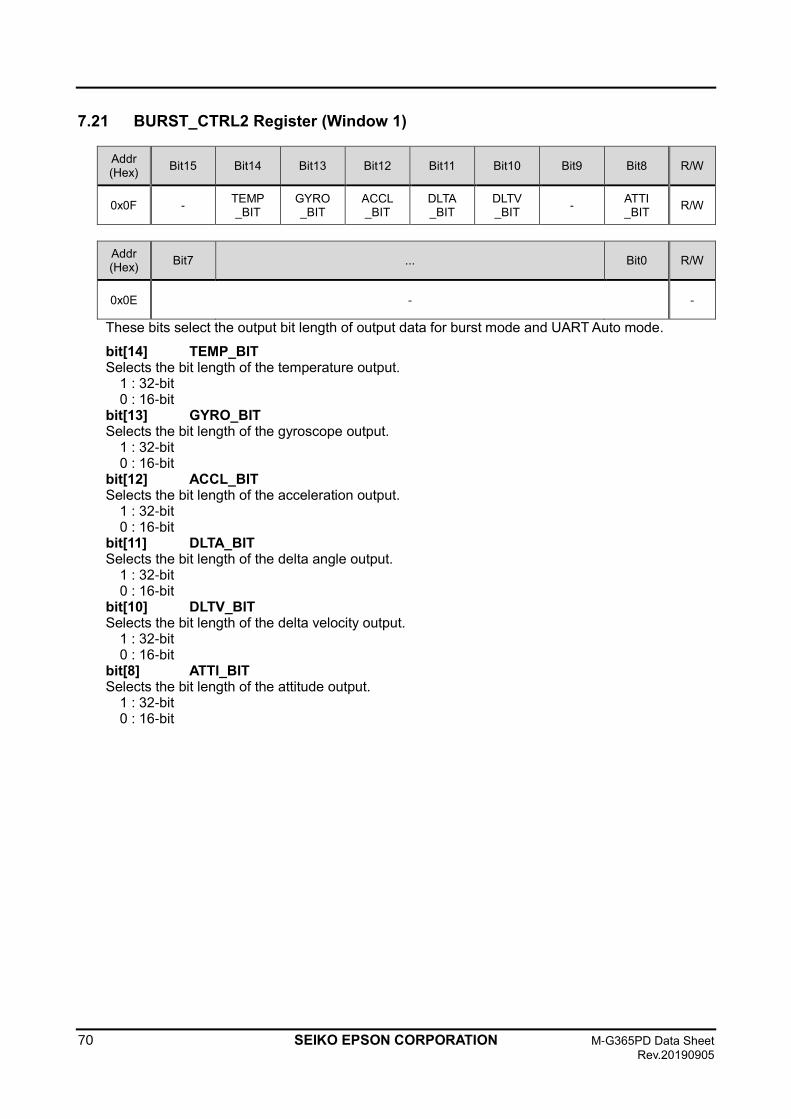
70 SEIKO EPSON CORPORATION M-G365PD Data Sheet
Rev.20190905
7.21 BURST_CTRL2 Register (Window 1)
Addr (Hex)
Bit15 Bit14 Bit13 Bit12 Bit11 Bit10 Bit9 Bit8 R/W
0x0F - TEMP _BIT
GYRO _BIT
ACCL _BIT
DLTA _BIT
DLTV _BIT
- ATTI _BIT
R/W
Addr (Hex)
Bit7 ... Bit0 R/W
0x0E - -
These bits select the output bit length of output data for burst mode and UART Auto mode.
bit[14] TEMP_BIT Selects the bit length of the temperature output.
1 : 32-bit 0 : 16-bit
bit[13] GYRO_BIT Selects the bit length of the gyroscope output.
1 : 32-bit 0 : 16-bit
bit[12] ACCL_BIT Selects the bit length of the acceleration output.
1 : 32-bit 0 : 16-bit
bit[11] DLTA_BIT Selects the bit length of the delta angle output.
1 : 32-bit 0 : 16-bit
bit[10] DLTV_BIT Selects the bit length of the delta velocity output.
1 : 32-bit 0 : 16-bit
bit[8] ATTI_BIT Selects the bit length of the attitude output.
1 : 32-bit 0 : 16-bit
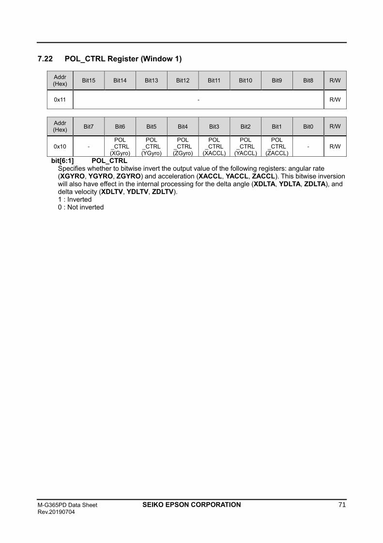
M-G365PD Data Sheet SEIKO EPSON CORPORATION 71 Rev.20190704
7.22 POL_CTRL Register (Window 1)
Addr (Hex)
Bit15 Bit14 Bit13 Bit12 Bit11 Bit10 Bit9 Bit8 R/W
0x11 - R/W
Addr (Hex)
Bit7 Bit6 Bit5 Bit4 Bit3 Bit2 Bit1 Bit0 R/W
0x10 - POL
_CTRL (XGyro)
POL _CTRL (YGyro)
POL _CTRL (ZGyro)
POL _CTRL
(XACCL)
POL _CTRL
(YACCL)
POL _CTRL
(ZACCL) - R/W
bit[6:1] POL_CTRL Specifies whether to bitwise invert the output value of the following registers: angular rate (XGYRO, YGYRO, ZGYRO) and acceleration (XACCL, YACCL, ZACCL). This bitwise inversion will also have effect in the internal processing for the delta angle (XDLTA, YDLTA, ZDLTA), and delta velocity (XDLTV, YDLTV, ZDLTV). 1 : Inverted 0 : Not inverted
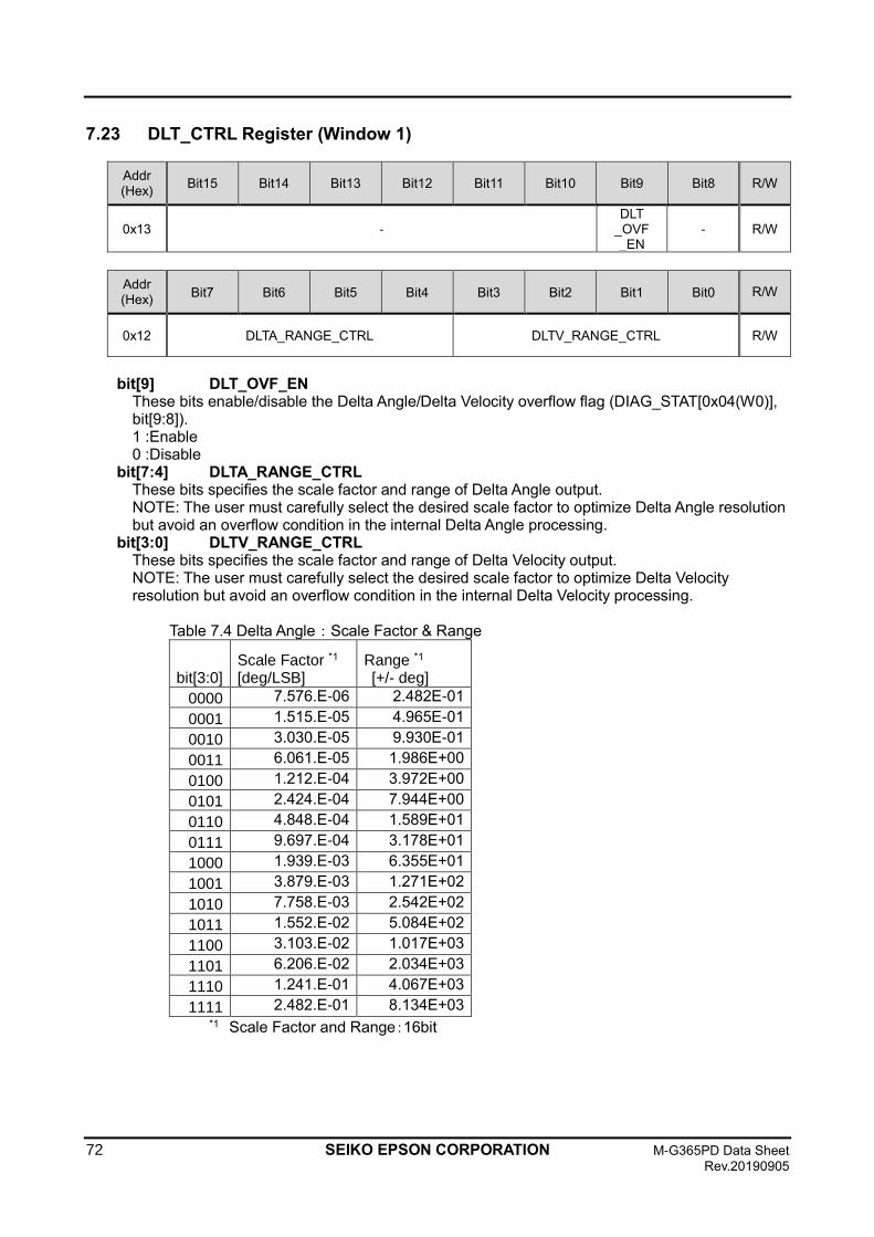
72 SEIKO EPSON CORPORATION M-G365PD Data Sheet
Rev.20190905
7.23 DLT_CTRL Register (Window 1)
Addr (Hex)
Bit15 Bit14 Bit13 Bit12 Bit11 Bit10 Bit9 Bit8 R/W
0x13 - DLT
_OVF _EN
- R/W
Addr (Hex)
Bit7 Bit6 Bit5 Bit4 Bit3 Bit2 Bit1 Bit0 R/W
0x12 DLTA_RANGE_CTRL DLTV_RANGE_CTRL R/W
bit[9] DLT_OVF_EN
These bits enable/disable the Delta Angle/Delta Velocity overflow flag (DIAG_STAT[0x04(W0)], bit[9:8]). 1 :Enable 0 :Disable
bit[7:4] DLTA_RANGE_CTRL These bits specifies the scale factor and range of Delta Angle output. NOTE: The user must carefully select the desired scale factor to optimize Delta Angle resolution but avoid an overflow condition in the internal Delta Angle processing.
bit[3:0] DLTV_RANGE_CTRL These bits specifies the scale factor and range of Delta Velocity output. NOTE: The user must carefully select the desired scale factor to optimize Delta Velocity resolution but avoid an overflow condition in the internal Delta Velocity processing.
Table 7.4 Delta Angle:Scale Factor & Range
bit[3:0] Scale Factor *1 [deg/LSB]
Range *1 [+/- deg]
0000 7.576.E-06 2.482E-01
0001 1.515.E-05 4.965E-01
0010 3.030.E-05 9.930E-01
0011 6.061.E-05 1.986E+00
0100 1.212.E-04 3.972E+00
0101 2.424.E-04 7.944E+00
0110 4.848.E-04 1.589E+01
0111 9.697.E-04 3.178E+01
1000 1.939.E-03 6.355E+01
1001 3.879.E-03 1.271E+02
1010 7.758.E-03 2.542E+02
1011 1.552.E-02 5.084E+02
1100 3.103.E-02 1.017E+03
1101 6.206.E-02 2.034E+03
1110 1.241.E-01 4.067E+03
1111 2.482.E-01 8.134E+03 *1 Scale Factor and Range:16bit
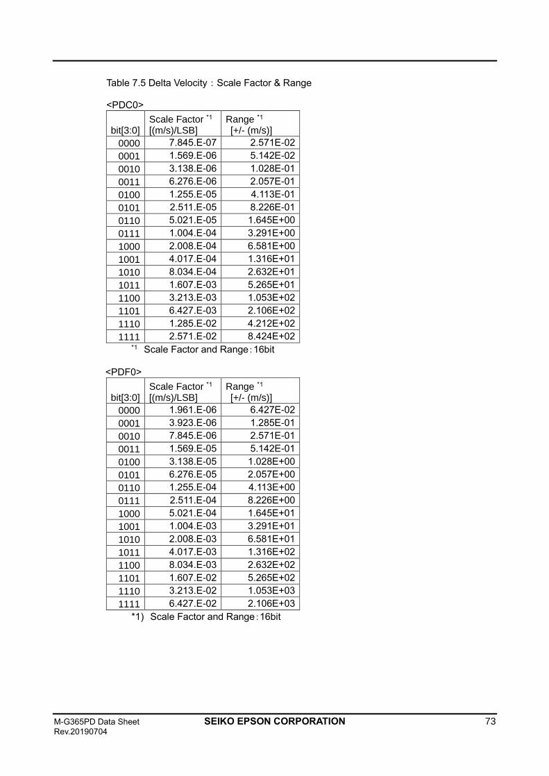
M-G365PD Data Sheet SEIKO EPSON CORPORATION 73 Rev.20190704
Table 7.5 Delta Velocity:Scale Factor & Range <PDC0>
bit[3:0] Scale Factor *1 [(m/s)/LSB]
Range *1 [+/- (m/s)]
0000 7.845.E-07 2.571E-02
0001 1.569.E-06 5.142E-02
0010 3.138.E-06 1.028E-01
0011 6.276.E-06 2.057E-01
0100 1.255.E-05 4.113E-01
0101 2.511.E-05 8.226E-01
0110 5.021.E-05 1.645E+00
0111 1.004.E-04 3.291E+00
1000 2.008.E-04 6.581E+00
1001 4.017.E-04 1.316E+01
1010 8.034.E-04 2.632E+01
1011 1.607.E-03 5.265E+01
1100 3.213.E-03 1.053E+02
1101 6.427.E-03 2.106E+02
1110 1.285.E-02 4.212E+02
1111 2.571.E-02 8.424E+02 *1 Scale Factor and Range:16bit
<PDF0>
bit[3:0] Scale Factor *1 [(m/s)/LSB]
Range *1 [+/- (m/s)]
0000 1.961.E-06 6.427E-02
0001 3.923.E-06 1.285E-01
0010 7.845.E-06 2.571E-01
0011 1.569.E-05 5.142E-01
0100 3.138.E-05 1.028E+00
0101 6.276.E-05 2.057E+00
0110 1.255.E-04 4.113E+00
0111 2.511.E-04 8.226E+00
1000 5.021.E-04 1.645E+01
1001 1.004.E-03 3.291E+01
1010 2.008.E-03 6.581E+01
1011 4.017.E-03 1.316E+02
1100 8.034.E-03 2.632E+02
1101 1.607.E-02 5.265E+02
1110 3.213.E-02 1.053E+03
1111 6.427.E-02 2.106E+03
*1) Scale Factor and Range:16bit
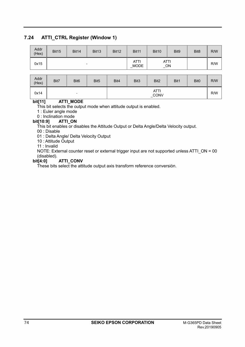
74 SEIKO EPSON CORPORATION M-G365PD Data Sheet
Rev.20190905
7.24 ATTI_CTRL Register (Window 1)
Addr (Hex)
Bit15 Bit14 Bit13 Bit12 Bit11 Bit10 Bit9 Bit8 R/W
0x15 - ATTI
_MODE ATTI _ON
R/W
Addr (Hex)
Bit7 Bit6 Bit5 Bit4 Bit3 Bit2 Bit1 Bit0 R/W
0x14 - ATTI
_CONV R/W
bit[11] ATTI_MODE This bit selects the output mode when attitude output is enabled. 1 : Euler angle mode 0 : Inclination mode
bit[10:9] ATTI_ON This bit enables or disables the Attitude Output or Delta Angle/Delta Velocity output. 00 : Disable 01 : Delta Angle/ Delta Velocity Output 10 : Attitude Output 11 : Invalid NOTE: External counter reset or external trigger input are not supported unless ATTI_ON = 00 (disabled).
bit[4:0] ATTI_CONV These bits select the attitude output axis transform reference conversión.
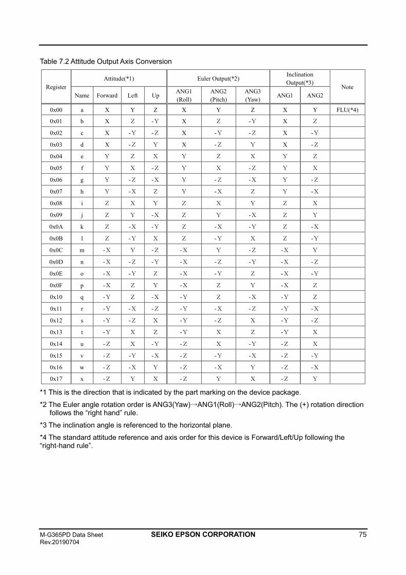
M-G365PD Data Sheet SEIKO EPSON CORPORATION 75 Rev.20190704
Table 7.2 Attitude Output Axis Conversion
Register
Attitude(*1) Euler Output(*2) Inclination
Output(*3) Note
Name Forward Left Up ANG1
(Roll)
ANG2
(Pitch)
ANG3
(Yaw) ANG1 ANG2
0x00 a X Y Z X Y Z X Y FLU(*4)
0x01 b X Z -Y X Z -Y X Z
0x02 c X -Y -Z X -Y -Z X -Y
0x03 d X -Z Y X -Z Y X -Z
0x04 e Y Z X Y Z X Y Z
0x05 f Y X -Z Y X -Z Y X
0x06 g Y -Z -X Y -Z -X Y -Z
0x07 h Y -X Z Y -X Z Y -X
0x08 i Z X Y Z X Y Z X
0x09 j Z Y -X Z Y -X Z Y
0x0A k Z -X -Y Z -X -Y Z -X
0x0B l Z -Y X Z -Y X Z -Y
0x0C m -X Y -Z -X Y -Z -X Y
0x0D n -X -Z -Y -X -Z -Y -X -Z
0x0E o -X -Y Z -X -Y Z -X -Y
0x0F p -X Z Y -X Z Y -X Z
0x10 q -Y Z -X -Y Z -X -Y Z
0x11 r -Y -X -Z -Y -X -Z -Y -X
0x12 s -Y -Z X -Y -Z X -Y -Z
0x13 t -Y X Z -Y X Z -Y X
0x14 u -Z X -Y -Z X -Y -Z X
0x15 v -Z -Y -X -Z -Y -X -Z -Y
0x16 w -Z -X Y -Z -X Y -Z -X
0x17 x -Z Y X -Z Y X -Z Y
*1 This is the direction that is indicated by the part marking on the device package.
*2 The Euler angle rotation order is ANG3(Yaw)→ANG1(Roll)→ANG2(Pitch). The (+) rotation direction follows the “right hand” rule.
*3 The inclination angle is referenced to the horizontal plane.
*4 The standard attitude reference and axis order for this device is Forward/Left/Up following the “right-hand rule”.
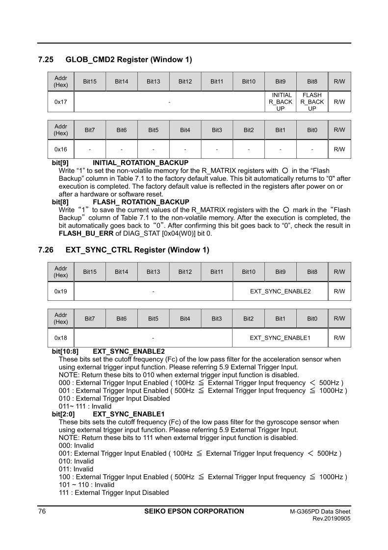
76 SEIKO EPSON CORPORATION M-G365PD Data Sheet
Rev.20190905
7.25 GLOB_CMD2 Register (Window 1)
Addr (Hex)
Bit15 Bit14 Bit13 Bit12 Bit11 Bit10 Bit9 Bit8 R/W
0x17 - INITIAL R_BACK
UP
FLASH R_BACK
UP R/W
Addr (Hex)
Bit7 Bit6 Bit5 Bit4 Bit3 Bit2 Bit1 Bit0 R/W
0x16 - - - - - - - - R/W
bit[9] INITIAL_ROTATION_BACKUP Write “1” to set the non-volatile memory for the R_MATRIX registers with ○ in the “Flash Backup” column in Table 7.1 to the factory default value. This bit automatically returns to “0" after execution is completed. The factory default value is reflected in the registers after power on or after a hardware or software reset.
bit[8] FLASH_ ROTATION_BACKUP Write “1” to save the current values of the R_MATRIX registers with the ○ mark in the “Flash Backup” column of Table 7.1 to the non-volatile memory. After the execution is completed, the bit automatically goes back to “0”. After confirming this bit goes back to “0”, check the result in FLASH_BU_ERR of DIAG_STAT [0x04(W0)] bit 0.
7.26 EXT_SYNC_CTRL Register (Window 1)
Addr (Hex)
Bit15 Bit14 Bit13 Bit12 Bit11 Bit10 Bit9 Bit8 R/W
0x19 - EXT_SYNC_ENABLE2 R/W
Addr (Hex)
Bit7 Bit6 Bit5 Bit4 Bit3 Bit2 Bit1 Bit0 R/W
0x18 - EXT_SYNC_ENABLE1 R/W
bit[10:8] EXT_SYNC_ENABLE2 These bits set the cutoff frequency (Fc) of the low pass filter for the acceleration sensor when using external trigger input function. Please referring 5.9 External Trigger Input. NOTE: Return these bits to 010 when external trigger input function is disabled. 000 : External Trigger Input Enabled ( 100Hz ≦ External Trigger Input frequency < 500Hz ) 001 : External Trigger Input Enabled ( 500Hz ≦ External Trigger Input frequency ≦ 1000Hz ) 010 : External Trigger Input Disabled 011~ 111 : Invalid
bit[2:0] EXT_SYNC_ENABLE1 These bits sets the cutoff frequency (Fc) of the low pass filter for the gyroscope sensor when using external trigger input function. Please referring 5.9 External Trigger Input. NOTE: Return these bits to 111 when external trigger input function is disabled. 000: Invalid 001: External Trigger Input Enabled ( 100Hz ≦ External Trigger Input frequency < 500Hz ) 010: Invalid 011: Invalid 100 : External Trigger Input Enabled ( 500Hz ≦ External Trigger Input frequency ≦ 1000Hz ) 101 ~ 110 : Invalid 111 : External Trigger Input Disabled
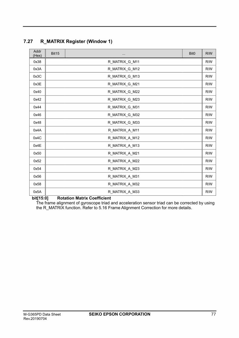
M-G365PD Data Sheet SEIKO EPSON CORPORATION 77 Rev.20190704
7.27 R_MATRIX Register (Window 1)
Addr (Hex)
Bit15 ... Bit0 R/W
0x38 R_MATRIX_G_M11 R/W
0x3A R_MATRIX_G_M12 R/W
0x3C R_MATRIX_G_M13 R/W
0x3E R_MATRIX_G_M21 R/W
0x40 R_MATRIX_G_M22 R/W
0x42 R_MATRIX_G_M23 R/W
0x44 R_MATRIX_G_M31 R/W
0x46 R_MATRIX_G_M32 R/W
0x48 R_MATRIX_G_M33 R/W
0x4A R_MATRIX_A_M11 R/W
0x4C R_MATRIX_A_M12 R/W
0x4E R_MATRIX_A_M13 R/W
0x50 R_MATRIX_A_M21 R/W
0x52 R_MATRIX_A_M22 R/W
0x54 R_MATRIX_A_M23 R/W
0x56 R_MATRIX_A_M31 R/W
0x58 R_MATRIX_A_M32 R/W
0x5A R_MATRIX_A_M33 R/W
bit[15:0] Rotation Matrix Coefficient The frame alignment of gyroscope triad and acceleration sensor triad can be corrected by using the R_MATRIX function. Refer to 5.16 Frame Alignment Correction for more details.
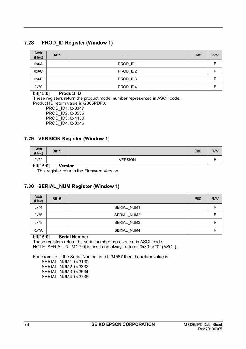
78 SEIKO EPSON CORPORATION M-G365PD Data Sheet
Rev.20190905
7.28 PROD_ID Register (Window 1)
Addr (Hex)
Bit15 ... Bit0 R/W
0x6A PROD_ID1 R
0x6C PROD_ID2 R
0x6E PROD_ID3 R
0x70 PROD_ID4 R
bit[15:0] Product ID These registers return the product model number represented in ASCII code. Product ID return value is G365PDF0.
PROD_ID1:0x3347 PROD_ID2:0x3536 PROD_ID3:0x4450 PROD_ID4:0x3046
7.29 VERSION Register (Window 1)
Addr (Hex)
Bit15 ... Bit0 R/W
0x72 VERSION R
bit[15:0] Version This register returns the Firmware Version
7.30 SERIAL_NUM Register (Window 1)
Addr (Hex)
Bit15 ... Bit0 R/W
0x74 SERIAL_NUM1 R
0x76 SERIAL_NUM2 R
0x78 SERIAL_NUM3 R
0x7A SERIAL_NUM4 R
bit[15:0] Serial Number These registers return the serial number represented in ASCII code. NOTE: SERIAL_NUM1[7:0] is fixed and always returns 0x30 or “0” (ASCII). For example, if the Serial Number is 01234567 then the return value is:
SERIAL_NUM1:0x3130 SERIAL_NUM2:0x3332 SERIAL_NUM3:0x3534 SERIAL_NUM4:0x3736
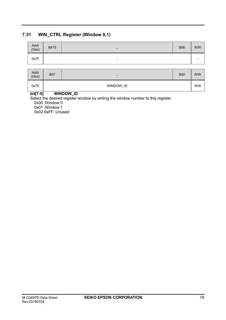
M-G365PD Data Sheet SEIKO EPSON CORPORATION 79 Rev.20190704
7.31 WIN_CTRL Register (Window 0,1)
Addr (Hex)
Bit15 ... Bit8 R/W
0x7F - -
Addr (Hex)
Bit7 ... Bit0 R/W
0x7E WINDOW_ID R/W
bit[7:0] WINDOW_ID Select the desired register window by writing the window number to this register.
0x00 :Window 0 0x01 :Window 1 0x02-0xFF: Unused
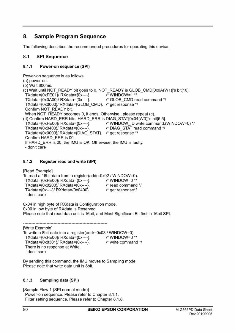
80 SEIKO EPSON CORPORATION M-G365PD Data Sheet
Rev.20190905
8. Sample Program Sequence
The following describes the recommended procedures for operating this device.
8.1 SPI Sequence
8.1.1 Power-on sequence (SPI)
Power-on sequence is as follows. (a) power-on. (b) Wait 800ms. (c) Wait until NOT_READY bit goes to 0. NOT_READY is GLOB_CMD[0x0A(W1)]'s bit[10]. TXdata={0xFE01}/ RXdata={0x----}. /* WINDOW=1 */ TXdata={0x0A00}/ RXdata={0x----}. /* GLOB_CMD read command */ TXdata={0x0000}/ RXdata={GLOB_CMD}. /* get response */ Confirm NOT_READY bit. When NOT_READY becomes 0, it ends. Otherwise , please repeat (c). (d) Confirm HARD_ERR bits. HARD_ERR is DIAG_STAT[0x04(W0)]'s bit[6:5]. TXdata={0xFE00}/ RXdata={0x----}. /* WINDOW_ID write command.(WINDOW=0) */ TXdata={0x0400}/ RXdata={0x----}. /* DIAG_STAT read command */ TXdata={0x0000}/ RXdata={DIAG_STAT}. /* get response */ Confirm HARD_ERR is 00. If HARD_ERR is 00, the IMU is OK. Otherwise, the IMU is faulty. -:don't care 8.1.2 Register read and write (SPI)
[Read Example] To read a 16bit-data from a register(addr=0x02 / WINDOW=0). TXdata={0xFE00}/ RXdata={0x----}. /* WINDOW=0 */ TXdata={0x0200}/ RXdata={0x----}. /* read command */ TXdata={0x----}/ RXdata={0x0400}. /* get response*/ -:don't care 0x04 in high byte of RXdata is Configuration mode. 0x00 in low byte of RXdata is Reserved. Please note that read data unit is 16bit, and Most Significant Bit first in 16bit SPI. ------------------------------------------------------------- [Write Example] To write a 8bit-data into a register(addr=0x03 / WINDOW=0). TXdata={0xFE00}/ RXdata={0x----}. /* WINDOW=0 */ TXdata={0x8301}/ RXdata={0x----}. /* write command */ There is no response at Write. -:don't care By sending this command, the IMU moves to Sampling mode. Please note that write data unit is 8bit. 8.1.3 Sampling data (SPI)
[Sample Flow 1 (SPI normal mode)] Power-on sequence. Please refer to Chapter 8.1.1. Filter setting sequence. Please refer to Chapter 8.1.8.
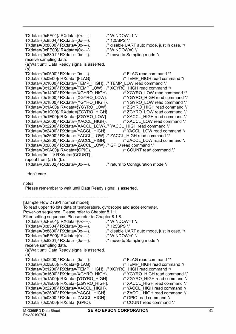
M-G365PD Data Sheet SEIKO EPSON CORPORATION 81 Rev.20190704
TXdata={0xFE01}/ RXdata={0x----}. /* WINDOW=1 */ TXdata={0x8504}/ RXdata={0x----}. /* 125SPS */ TXdata={0x8800}/ RXdata={0x----}. /* disable UART auto mode, just in case. */ TXdata={0xFE00}/ RXdata={0x----}. /* WINDOW=0 */ TXdata={0x8301}/ RXdata={0x----}. /* move to Sampling mode */ receive sampling data. (a)Wait until Data Ready signal is asserted. (b) TXdata={0x0600}/ RXdata={0x----}. /* FLAG read command */ TXdata={0x0E00}/ RXdata={FLAG}. /* TEMP_HIGH read command */ TXdata={0x1000}/ RXdata={TEMP_HIGH}. /* TEMP_LOW read command */ TXdata={0x1200}/ RXdata={TEMP_LOW}. /* XGYRO_HIGH read command */ TXdata={0x1400}/ RXdata={XGYRO_HIGH}. /* XGYRO_LOW read command */ TXdata={0x1600}/ RXdata={XGYRO_LOW}. /* YGYRO_HIGH read command */ TXdata={0x1800}/ RXdata={YGYRO_HIGH}. /* YGYRO_LOW read command */ TXdata={0x1A00}/ RXdata={YGYRO_LOW}. /* ZGYRO_HIGH read command */ TXdata={0x1C00}/ RXdata={ZGYRO_HIGH}. /* ZGYRO_LOW read command */ TXdata={0x1E00}/ RXdata={ZGYRO_LOW}. /* XACCL_HIGH read command */ TXdata={0x2000}/ RXdata={XACCL_HIGH}. /* XACCL_LOW read command */ TXdata={0x2200}/ RXdata={XACCL_LOW}. /* YACCL_HIGH read command */ TXdata={0x2400}/ RXdata={YACCL_HIGH}. /* YACCL_LOW read command */ TXdata={0x2600}/ RXdata={YACCL_LOW}. /* ZACCL_HIGH read command */ TXdata={0x2800}/ RXdata={ZACCL_HIGH}. /* ZACCL_LOW read command */ TXdata={0x0800}/ RXdata={ZACCL_LOW}. /* GPIO read command */ TXdata={0x0A00}/ RXdata={GPIO}. /* COUNT read command */ TXdata={0x----}/ RXdata={COUNT}. repeat from (a) to (b). TXdata={0x8302}/ RXdata={0x----}. /* return to Configuration mode */ -:don't care notes Please remember to wait until Data Ready signal is asserted. ------------------------------------------------------------- [Sample Flow 2 (SPI normal mode)] To read upper 16 bits data of temperature, gyroscope and accelerometer. Power-on sequence. Please refer to Chapter 8.1.1. Filter setting sequence. Please refer to Chapter 8.1.8. TXdata={0xFE01}/ RXdata={0x----}. /* WINDOW=1 */ TXdata={0x8504}/ RXdata={0x----}. /* 125SPS */ TXdata={0x8800}/ RXdata={0x----}. /* disable UART auto mode, just in case. */ TXdata={0xFE00}/ RXdata={0x----}. /* WINDOW=0 */ TXdata={0x8301}/ RXdata={0x----}. /* move to Sampling mode */ receive sampling data. (a)Wait until Data Ready signal is asserted. (b) TXdata={0x0600}/ RXdata={0x----}. /* FLAG read command */ TXdata={0x0E00}/ RXdata={FLAG}. /* TEMP_HIGH read command */ TXdata={0x1200}/ RXdata={TEMP_HIGH}. /* XGYRO_HIGH read command */ TXdata={0x1600}/ RXdata={XGYRO_HIGH}. /* YGYRO_HIGH read command */ TXdata={0x1A00}/ RXdata={YGYRO_HIGH}. /* ZGYRO_HIGH read command */ TXdata={0x1E00}/ RXdata={ZGYRO_HIGH}. /* XACCL_HIGH read command */ TXdata={0x2200}/ RXdata={XACCL_HIGH}. /* YACCL_HIGH read command */ TXdata={0x2600}/ RXdata={YACCL_HIGH}. /* ZACCL_HIGH read command */ TXdata={0x0800}/ RXdata={ZACCL_HIGH}. /* GPIO read command */ TXdata={0x0A00}/ RXdata={GPIO}. /* COUNT read command */
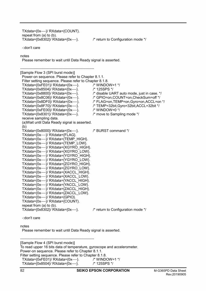
82 SEIKO EPSON CORPORATION M-G365PD Data Sheet
Rev.20190905
TXdata={0x----}/ RXdata={COUNT}. repeat from (a) to (b). TXdata={0x8302}/ RXdata={0x----}. /* return to Configuration mode */ -:don't care notes Please remember to wait until Data Ready signal is asserted. ------------------------------------------------------------- [Sample Flow 3 (SPI burst mode)] Power-on sequence. Please refer to Chapter 8.1.1. Filter setting sequence. Please refer to Chapter 8.1.8. TXdata={0xFE01}/ RXdata={0x----}. /* WINDOW=1 */ TXdata={0x8504}/ RXdata={0x----}. /* 125SPS */ TXdata={0x8800}/ RXdata={0x----}. /* disable UART auto mode, just in case. */ TXdata={0x8C06}/ RXdata={0x----}. /* GPIO=on,COUNT=on,CheckSum=off */ TXdata={0x8DF0}/ RXdata={0x----}. /* FLAG=on,TEMP=on,Gyro=on,ACCL=on */ TXdata={0x8F70}/ RXdata={0x----}. /* TEMP=32bit,Gyro=32bit,ACCL=32bit */ TXdata={0xFE00}/ RXdata={0x----}. /* WINDOW=0 */ TXdata={0x8301}/ RXdata={0x----}. /* move to Sampling mode */ receive sampling data. (a)Wait until Data Ready signal is asserted. (b) TXdata={0x8000}/ RXdata={0x----}. /* BURST command */ TXdata={0x----}/ RXdata={FLAG}. TXdata={0x----}/ RXdata={TEMP_HIGH}. TXdata={0x----}/ RXdata={TEMP_LOW}. TXdata={0x----}/ RXdata={XGYRO_HIGH}. TXdata={0x----}/ RXdata={XGYRO_LOW}. TXdata={0x----}/ RXdata={YGYRO_HIGH}. TXdata={0x----}/ RXdata={YGYRO_LOW}. TXdata={0x----}/ RXdata={ZGYRO_HIGH}. TXdata={0x----}/ RXdata={ZGYRO_LOW}. TXdata={0x----}/ RXdata={XACCL_HIGH}. TXdata={0x----}/ RXdata={XACCL_LOW}. TXdata={0x----}/ RXdata={YACCL_HIGH}. TXdata={0x----}/ RXdata={YACCL_LOW}. TXdata={0x----}/ RXdata={ZACCL_HIGH}. TXdata={0x----}/ RXdata={ZACCL_LOW}. TXdata={0x----}/ RXdata={GPIO}. TXdata={0x----}/ RXdata={COUNT}. repeat from (a) to (b). TXdata={0x8302}/ RXdata={0x----}. /* return to Configuration mode */ -:don't care notes Please remember to wait until Data Ready signal is asserted. ------------------------------------------------------------- [Sample Flow 4 (SPI burst mode)] To read upper 16 bits data of temperature, gyroscope and accelerometer. Power-on sequence. Please refer to Chapter 8.1.1. Filter setting sequence. Please refer to Chapter 8.1.8. TXdata={0xFE01}/ RXdata={0x----}. /* WINDOW=1 */ TXdata={0x8504}/ RXdata={0x----}. /* 125SPS */
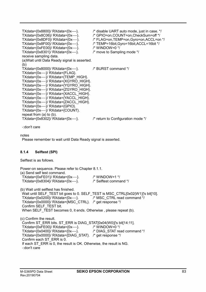
M-G365PD Data Sheet SEIKO EPSON CORPORATION 83 Rev.20190704
TXdata={0x8800}/ RXdata={0x----}. /* disable UART auto mode, just in case. */ TXdata={0x8C06}/ RXdata={0x----}. /* GPIO=on,COUNT=on,CheckSum=off */ TXdata={0x8DF0}/ RXdata={0x----}. /* FLAG=on,TEMP=on,Gyro=on,ACCL=on */ TXdata={0x8F00}/ RXdata={0x----}. /* TEMP=16bit,Gyro=16bit,ACCL=16bit */ TXdata={0xFE00}/ RXdata={0x----}. /* WINDOW=0 */ TXdata={0x8301}/ RXdata={0x----}. /* move to Sampling mode */ receive sampling data. (a)Wait until Data Ready signal is asserted. (b) TXdata={0x8000}/ RXdata={0x----}. /* BURST command */ TXdata={0x----}/ RXdata={FLAG}. TXdata={0x----}/ RXdata={TEMP_HIGH}. TXdata={0x----}/ RXdata={XGYRO_HIGH}. TXdata={0x----}/ RXdata={YGYRO_HIGH}. TXdata={0x----}/ RXdata={ZGYRO_HIGH}. TXdata={0x----}/ RXdata={XACCL_HIGH}. TXdata={0x----}/ RXdata={YACCL_HIGH}. TXdata={0x----}/ RXdata={ZACCL_HIGH}. TXdata={0x----}/ RXdata={GPIO}. TXdata={0x----}/ RXdata={COUNT}. repeat from (a) to (b). TXdata={0x8302}/ RXdata={0x----}. /* return to Configuration mode */ -:don't care notes Please remember to wait until Data Ready signal is asserted. 8.1.4 Selftest (SPI)
Selftest is as follows. Power-on sequence. Please refer to Chapter 8.1.1. (a) Send self test command. TXdata={0xFE01}/ RXdata={0x----}. /* WINDOW=1 */ TXdata={0x8304}/ RXdata={0x----}. /* Selftest command */ (b) Wait until selftest has finished. Wait until SELF_TEST bit goes to 0. SELF_TEST is MSC_CTRL[0x02(W1)]'s bit[10]. TXdata={0x0200}/ RXdata={0x----}. /* MSC_CTRL read command */ TXdata={0x0000}/ RXdata={MSC_CTRL}. /* get response */ Confirm SELF_TEST bit. When SELF_TEST becomes 0, it ends. Otherwise , please repeat (b). (c) Confirm the result. Confirm ST_ERR bits. ST_ERR is DIAG_STAT[0x04(W0)]'s bit[14:11]. TXdata={0xFE00}/ RXdata={0x----}. /* WINDOW=0 */ TXdata={0x0400}/ RXdata={0x----}. /* DIAG_STAT read command */ TXdata={0x0000}/ RXdata={DIAG_STAT}. /* get response */ Confirm each ST_ERR is 0. If each ST_ERR is 0, the result is OK. Otherwise, the result is NG. -:don't care
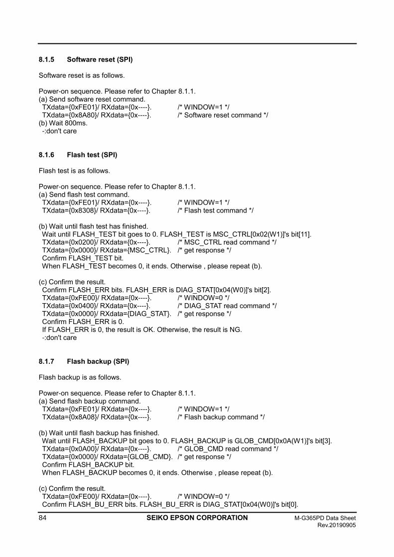
84 SEIKO EPSON CORPORATION M-G365PD Data Sheet
Rev.20190905
8.1.5 Software reset (SPI)
Software reset is as follows. Power-on sequence. Please refer to Chapter 8.1.1. (a) Send software reset command. TXdata={0xFE01}/ RXdata={0x----}. /* WINDOW=1 */ TXdata={0x8A80}/ RXdata={0x----}. /* Software reset command */ (b) Wait 800ms. -:don't care 8.1.6 Flash test (SPI)
Flash test is as follows. Power-on sequence. Please refer to Chapter 8.1.1. (a) Send flash test command. TXdata={0xFE01}/ RXdata={0x----}. /* WINDOW=1 */ TXdata={0x8308}/ RXdata={0x----}. /* Flash test command */ (b) Wait until flash test has finished. Wait until FLASH_TEST bit goes to 0. FLASH_TEST is MSC_CTRL[0x02(W1)]'s bit[11]. TXdata={0x0200}/ RXdata={0x----}. /* MSC_CTRL read command */ TXdata={0x0000}/ RXdata={MSC_CTRL}. /* get response */ Confirm FLASH_TEST bit. When FLASH_TEST becomes 0, it ends. Otherwise , please repeat (b). (c) Confirm the result. Confirm FLASH_ERR bits. FLASH_ERR is DIAG_STAT[0x04(W0)]'s bit[2]. TXdata={0xFE00}/ RXdata={0x----}. /* WINDOW=0 */ TXdata={0x0400}/ RXdata={0x----}. /* DIAG_STAT read command */ TXdata={0x0000}/ RXdata={DIAG_STAT}. /* get response */ Confirm FLASH_ERR is 0. If FLASH_ERR is 0, the result is OK. Otherwise, the result is NG. -:don't care 8.1.7 Flash backup (SPI)
Flash backup is as follows. Power-on sequence. Please refer to Chapter 8.1.1. (a) Send flash backup command. TXdata={0xFE01}/ RXdata={0x----}. /* WINDOW=1 */ TXdata={0x8A08}/ RXdata={0x----}. /* Flash backup command */ (b) Wait until flash backup has finished. Wait until FLASH_BACKUP bit goes to 0. FLASH_BACKUP is GLOB_CMD[0x0A(W1)]'s bit[3]. TXdata={0x0A00}/ RXdata={0x----}. /* GLOB_CMD read command */ TXdata={0x0000}/ RXdata={GLOB_CMD}. /* get response */ Confirm FLASH_BACKUP bit. When FLASH_BACKUP becomes 0, it ends. Otherwise , please repeat (b). (c) Confirm the result. TXdata={0xFE00}/ RXdata={0x----}. /* WINDOW=0 */ Confirm FLASH_BU_ERR bits. FLASH_BU_ERR is DIAG_STAT[0x04(W0)]'s bit[0].
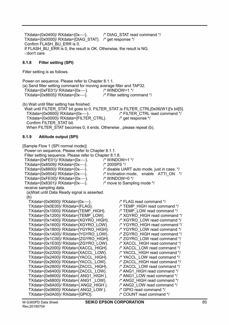
M-G365PD Data Sheet SEIKO EPSON CORPORATION 85 Rev.20190704
TXdata={0x0400}/ RXdata={0x----}. /* DIAG_STAT read command */ TXdata={0x0000}/ RXdata={DIAG_STAT}. /* get response */ Confirm FLASH_BU_ERR is 0. If FLASH_BU_ERR is 0, the result is OK. Otherwise, the result is NG. -:don't care 8.1.8 Filter setting (SPI)
Filter setting is as follows. Power-on sequence. Please refer to Chapter 8.1.1. (a) Send filter setting command for moving average filter and TAP32. TXdata={0xFE01}/ RXdata={0x----}. /* WINDOW=1 */ TXdata={0x8605}/ RXdata={0x----}. /* Filter setting command */ (b) Wait until filter setting has finished. Wait until FILTER_STAT bit goes to 0. FILTER_STAT is FILTER_CTRL[0x06(W1)]'s bit[5]. TXdata={0x0600}/ RXdata={0x----}. /* FILTER_CTRL read command */ TXdata={0x0000}/ RXdata={FILTER_CTRL}. /* get response */ Confirm FILTER_STAT bit. When FILTER_STAT becomes 0, it ends. Otherwise , please repeat (b). 8.1.9 Attitude output (SPI)
[Sample Flow 1 (SPI normal mode)] Power-on sequence. Please refer to Chapter 8.1.1. Filter setting sequence. Please refer to Chapter 8.1.8. TXdata={0xFE01}/ RXdata={0x----}. /* WINDOW=1 */ TXdata={0x8509}/ RXdata={0x----}. /* 200SPS */ TXdata={0x8800}/ RXdata={0x----}. /* disable UART auto mode, just in case. */ TXdata={0x9504}/ RXdata={0x----}. /* Inclination mode, enable ATTI_ON */
TXdata={0xFE00}/ RXdata={0x----}. /* WINDOW=0 */ TXdata={0x8301}/ RXdata={0x----}. /* move to Sampling mode */ receive sampling data. (a)Wait until Data Ready signal is asserted. (b) TXdata={0x0600}/ RXdata={0x----}. /* FLAG read command */ TXdata={0x0E00}/ RXdata={FLAG}. /* TEMP_HIGH read command */ TXdata={0x1000}/ RXdata={TEMP_HIGH}. /* TEMP_LOW read command */ TXdata={0x1200}/ RXdata={TEMP_LOW}. /* XGYRO_HIGH read command */ TXdata={0x1400}/ RXdata={XGYRO_HIGH}. /* XGYRO_LOW read command */ TXdata={0x1600}/ RXdata={XGYRO_LOW}. /* YGYRO_HIGH read command */ TXdata={0x1800}/ RXdata={YGYRO_HIGH}. /* YGYRO_LOW read command */ TXdata={0x1A00}/ RXdata={YGYRO_LOW}. /* ZGYRO_HIGH read command */ TXdata={0x1C00}/ RXdata={ZGYRO_HIGH}. /* ZGYRO_LOW read command */ TXdata={0x1E00}/ RXdata={ZGYRO_LOW}. /* XACCL_HIGH read command */ TXdata={0x2000}/ RXdata={XACCL_HIGH}. /* XACCL_LOW read command */ TXdata={0x2200}/ RXdata={XACCL_LOW}. /* YACCL_HIGH read command */ TXdata={0x2400}/ RXdata={YACCL_HIGH}. /* YACCL_LOW read command */ TXdata={0x2600}/ RXdata={YACCL_LOW}. /* ZACCL_HIGH read command */ TXdata={0x2800}/ RXdata={ZACCL_HIGH}. /* ZACCL_LOW read command */ TXdata={0x6400}/ RXdata={ZACCL_LOW}. /* ANG1_HIGH read command */ TXdata={0x6600}/ RXdata={ ANG1_HIGH }. /* ANG1_LOW read command */ TXdata={0x6800}/ RXdata={ ANG1 _LOW}. /* ANG2_HIGH read command */ TXdata={0x6A00}/ RXdata={ ANG2_HIGH }. /* ANG2_LOW read command */ TXdata={0x0800}/ RXdata={ ANG2_LOW }. /* GPIO read command */ TXdata={0x0A00}/ RXdata={GPIO}. /* COUNT read command */
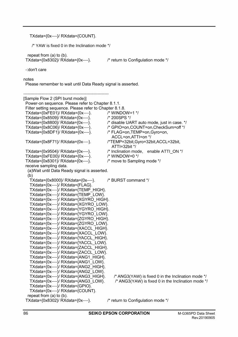
86 SEIKO EPSON CORPORATION M-G365PD Data Sheet
Rev.20190905
TXdata={0x----}/ RXdata={COUNT}.
/* YAW is fixed 0 in the Inclination mode */ repeat from (a) to (b). TXdata={0x8302}/ RXdata={0x----}. /* return to Configulation mode */ -:don't care notes Please remember to wait until Data Ready signal is asserted. ------------------------------------------------------------- [Sample Flow 2 (SPI burst mode)] Power-on sequence. Please refer to Chapter 8.1.1. Filter setting sequence. Please refer to Chapter 8.1.8. TXdata={0xFE01}/ RXdata={0x----}. /* WINDOW=1 */ TXdata={0x8509}/ RXdata={0x----}. /* 200SPS */ TXdata={0x8800}/ RXdata={0x----}. /* disable UART auto mode, just in case. */ TXdata={0x8C06}/ RXdata={0x----}. /* GPIO=on,COUNT=on,CheckSum=off */
TXdata={0x8DF1}/ RXdata={0x----}. /* FLAG=on,TEMP=on,Gyro=on, ACCL=on,ATTI=on */
TXdata={0x8F71}/ RXdata={0x----}. /*TEMP=32bit,Gyro=32bit,ACCL=32bit, ATTI=32bit */
TXdata={0x9504}/ RXdata={0x----}. /* Inclination mode, enable ATTI_ON */ TXdata={0xFE00}/ RXdata={0x----}. /* WINDOW=0 */ TXdata={0x8301}/ RXdata={0x----}. /* move to Sampling mode */ receive sampling data. (a)Wait until Data Ready signal is asserted. (b) TXdata={0x8000}/ RXdata={0x----}. /* BURST command */ TXdata={0x----}/ RXdata={FLAG}. TXdata={0x----}/ RXdata={TEMP_HIGH}. TXdata={0x----}/ RXdata={TEMP_LOW}. TXdata={0x----}/ RXdata={XGYRO_HIGH}. TXdata={0x----}/ RXdata={XGYRO_LOW}. TXdata={0x----}/ RXdata={YGYRO_HIGH}. TXdata={0x----}/ RXdata={YGYRO_LOW}. TXdata={0x----}/ RXdata={ZGYRO_HIGH}. TXdata={0x----}/ RXdata={ZGYRO_LOW}. TXdata={0x----}/ RXdata={XACCL_HIGH}. TXdata={0x----}/ RXdata={XACCL_LOW}. TXdata={0x----}/ RXdata={YACCL_HIGH}. TXdata={0x----}/ RXdata={YACCL_LOW}. TXdata={0x----}/ RXdata={ZACCL_HIGH}. TXdata={0x----}/ RXdata={ZACCL_LOW}.
TXdata={0x----}/ RXdata={ANG1_HIGH}. TXdata={0x----}/ RXdata={ANG1_LOW}. TXdata={0x----}/ RXdata={ANG2_HIGH}. TXdata={0x----}/ RXdata={ANG2_LOW}. TXdata={0x----}/ RXdata={ANG3_HIGH}. /* ANG3(YAW) is fixed 0 in the Inclination mode */ TXdata={0x----}/ RXdata={ANG3_LOW}. /* ANG3(YAW) is fixed 0 in the Inclination mode */
TXdata={0x----}/ RXdata={GPIO}. TXdata={0x----}/ RXdata={COUNT}. repeat from (a) to (b). TXdata={0x8302}/ RXdata={0x----}. /* return to Configulation mode */
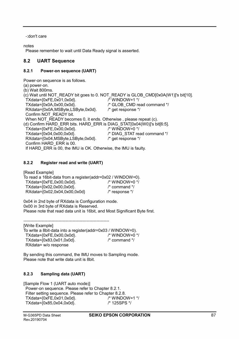
M-G365PD Data Sheet SEIKO EPSON CORPORATION 87 Rev.20190704
-:don't care notes Please remember to wait until Data Ready signal is asserted.
8.2 UART Sequence
8.2.1 Power-on sequence (UART)
Power-on sequence is as follows. (a) power-on. (b) Wait 800ms. (c) Wait until NOT_READY bit goes to 0. NOT_READY is GLOB_CMD[0x0A(W1)]'s bit[10]. TXdata={0xFE,0x01,0x0d}. /* WINDOW=1 */ TXdata={0x0A,0x00,0x0d}. /* GLOB_CMD read command */ RXdata={0x0A,MSByte,LSByte,0x0d}. /* get response */ Confirm NOT_READY bit. When NOT_READY becomes 0, it ends. Otherwise , please repeat (c). (d) Confirm HARD_ERR bits. HARD_ERR is DIAG_STAT[0x04(W0)]'s bit[6:5]. TXdata={0xFE,0x00,0x0d}. /* WINDOW=0 */ TXdata={0x04,0x00,0x0d}. /* DIAG_STAT read command */ RXdata={0x04,MSByte,LSByte,0x0d}. /* get response */ Confirm HARD_ERR is 00. If HARD_ERR is 00, the IMU is OK. Otherwise, the IMU is faulty. 8.2.2 Register read and write (UART)
[Read Example] To read a 16bit-data from a register(addr=0x02 / WINDOW=0). TXdata={0xFE,0x00,0x0d}. /* WINDOW=0 */ TXdata={0x02,0x00,0x0d}. /* command */ RXdata={0x02,0x04,0x00,0x0d} /* response */ 0x04 in 2nd byte of RXdata is Configuration mode. 0x00 in 3rd byte of RXdata is Reserved. Please note that read data unit is 16bit, and Most Significant Byte first. ------------------------------------------------------------- [Write Example] To write a 8bit-data into a register(addr=0x03 / WINDOW=0). TXdata={0xFE,0x00,0x0d}. /* WINDOW=0 */ TXdata={0x83,0x01,0x0d}. /* command */ RXdata= w/o response By sending this command, the IMU moves to Sampling mode. Please note that write data unit is 8bit. 8.2.3 Sampling data (UART)
[Sample Flow 1 (UART auto mode)] Power-on sequence. Please refer to Chapter 8.2.1. Filter setting sequence. Please refer to Chapter 8.2.8. TXdata={0xFE,0x01,0x0d}. /* WINDOW=1 */ TXdata={0x85,0x04,0x0d}. /* 125SPS */
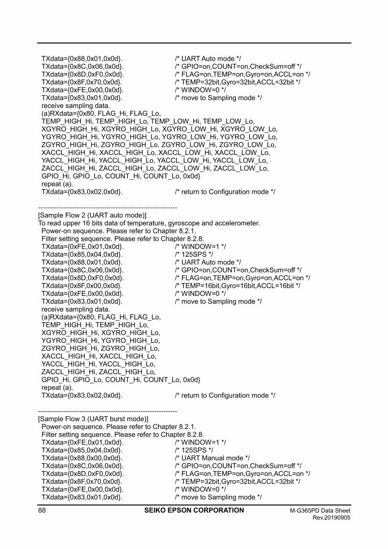
88 SEIKO EPSON CORPORATION M-G365PD Data Sheet
Rev.20190905
TXdata={0x88,0x01,0x0d}. /* UART Auto mode */ TXdata={0x8C,0x06,0x0d}. /* GPIO=on,COUNT=on,CheckSum=off */ TXdata={0x8D,0xF0,0x0d}. /* FLAG=on,TEMP=on,Gyro=on,ACCL=on */ TXdata={0x8F,0x70,0x0d}. /* TEMP=32bit,Gyro=32bit,ACCL=32bit */ TXdata={0xFE,0x00,0x0d}. /* WINDOW=0 */ TXdata={0x83,0x01,0x0d}. /* move to Sampling mode */ receive sampling data. (a)RXdata={0x80, FLAG_Hi, FLAG_Lo, TEMP_HIGH_Hi, TEMP_HIGH_Lo, TEMP_LOW_Hi, TEMP_LOW_Lo, XGYRO_HIGH_Hi, XGYRO_HIGH_Lo, XGYRO_LOW_Hi, XGYRO_LOW_Lo, YGYRO_HIGH_Hi, YGYRO_HIGH_Lo, YGYRO_LOW_Hi, YGYRO_LOW_Lo, ZGYRO_HIGH_Hi, ZGYRO_HIGH_Lo, ZGYRO_LOW_Hi, ZGYRO_LOW_Lo, XACCL_HIGH_Hi, XACCL_HIGH_Lo, XACCL_LOW_Hi, XACCL_LOW_Lo, YACCL_HIGH_Hi, YACCL_HIGH_Lo, YACCL_LOW_Hi, YACCL_LOW_Lo, ZACCL_HIGH_Hi, ZACCL_HIGH_Lo, ZACCL_LOW_Hi, ZACCL_LOW_Lo, GPIO_Hi, GPIO_Lo, COUNT_Hi, COUNT_Lo, 0x0d} repeat (a). TXdata={0x83,0x02,0x0d}. /* return to Configuration mode */ ------------------------------------------------------------- [Sample Flow 2 (UART auto mode)] To read upper 16 bits data of temperature, gyroscope and accelerometer. Power-on sequence. Please refer to Chapter 8.2.1. Filter setting sequence. Please refer to Chapter 8.2.8. TXdata={0xFE,0x01,0x0d}. /* WINDOW=1 */ TXdata={0x85,0x04,0x0d}. /* 125SPS */ TXdata={0x88,0x01,0x0d}. /* UART Auto mode */ TXdata={0x8C,0x06,0x0d}. /* GPIO=on,COUNT=on,CheckSum=off */ TXdata={0x8D,0xF0,0x0d}. /* FLAG=on,TEMP=on,Gyro=on,ACCL=on */ TXdata={0x8F,0x00,0x0d}. /* TEMP=16bit,Gyro=16bit,ACCL=16bit */ TXdata={0xFE,0x00,0x0d}. /* WINDOW=0 */ TXdata={0x83,0x01,0x0d}. /* move to Sampling mode */ receive sampling data. (a)RXdata={0x80, FLAG_Hi, FLAG_Lo, TEMP_HIGH_Hi, TEMP_HIGH_Lo, XGYRO_HIGH_Hi, XGYRO_HIGH_Lo, YGYRO_HIGH_Hi, YGYRO_HIGH_Lo, ZGYRO_HIGH_Hi, ZGYRO_HIGH_Lo, XACCL_HIGH_Hi, XACCL_HIGH_Lo, YACCL_HIGH_Hi, YACCL_HIGH_Lo, ZACCL_HIGH_Hi, ZACCL_HIGH_Lo, GPIO_Hi, GPIO_Lo, COUNT_Hi, COUNT_Lo, 0x0d} repeat (a). TXdata={0x83,0x02,0x0d}. /* return to Configuration mode */ ------------------------------------------------------------- [Sample Flow 3 (UART burst mode)] Power-on sequence. Please refer to Chapter 8.2.1. Filter setting sequence. Please refer to Chapter 8.2.8. TXdata={0xFE,0x01,0x0d}. /* WINDOW=1 */ TXdata={0x85,0x04,0x0d}. /* 125SPS */ TXdata={0x88,0x00,0x0d}. /* UART Manual mode */ TXdata={0x8C,0x06,0x0d}. /* GPIO=on,COUNT=on,CheckSum=off */ TXdata={0x8D,0xF0,0x0d}. /* FLAG=on,TEMP=on,Gyro=on,ACCL=on */ TXdata={0x8F,0x70,0x0d}. /* TEMP=32bit,Gyro=32bit,ACCL=32bit */ TXdata={0xFE,0x00,0x0d}. /* WINDOW=0 */ TXdata={0x83,0x01,0x0d}. /* move to Sampling mode */
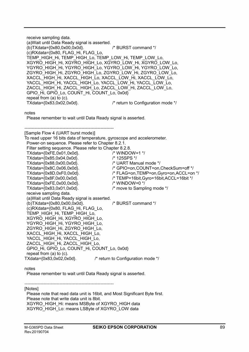
M-G365PD Data Sheet SEIKO EPSON CORPORATION 89 Rev.20190704
receive sampling data. (a)Wait until Data Ready signal is asserted. (b)TXdata={0x80,0x00,0x0d}. /* BURST command */ (c)RXdata={0x80, FLAG_Hi, FLAG_Lo, TEMP_HIGH_Hi, TEMP_HIGH_Lo, TEMP_LOW_Hi, TEMP_LOW_Lo, XGYRO_HIGH_Hi, XGYRO_HIGH_Lo, XGYRO_LOW_Hi, XGYRO_LOW_Lo, YGYRO_HIGH_Hi, YGYRO_HIGH_Lo, YGYRO_LOW_Hi, YGYRO_LOW_Lo, ZGYRO_HIGH_Hi, ZGYRO_HIGH_Lo, ZGYRO_LOW_Hi, ZGYRO_LOW_Lo, XACCL_HIGH_Hi, XACCL_HIGH_Lo, XACCL_LOW_Hi, XACCL_LOW_Lo, YACCL_HIGH_Hi, YACCL_HIGH_Lo, YACCL_LOW_Hi, YACCL_LOW_Lo, ZACCL_HIGH_Hi, ZACCL_HIGH_Lo, ZACCL_LOW_Hi, ZACCL_LOW_Lo, GPIO_Hi, GPIO_Lo, COUNT_Hi, COUNT_Lo, 0x0d} repeat from (a) to (c). TXdata={0x83,0x02,0x0d}. /* return to Configuration mode */ notes Please remember to wait until Data Ready signal is asserted. ------------------------------------------------------------- [Sample Flow 4 (UART burst mode)] To read upper 16 bits data of temperature, gyroscope and accelerometer. Power-on sequence. Please refer to Chapter 8.2.1. Filter setting sequence. Please refer to Chapter 8.2.8. TXdata={0xFE,0x01,0x0d}. /* WINDOW=1 */ TXdata={0x85,0x04,0x0d}. /* 125SPS */ TXdata={0x88,0x00,0x0d}. /* UART Manual mode */ TXdata={0x8C,0x06,0x0d}. /* GPIO=on,COUNT=on,CheckSum=off */ TXdata={0x8D,0xF0,0x0d}. /* FLAG=on,TEMP=on,Gyro=on,ACCL=on */ TXdata={0x8F,0x00,0x0d}. /* TEMP=16bit,Gyro=16bit,ACCL=16bit */ TXdata={0xFE,0x00,0x0d}. /* WINDOW=0 */ TXdata={0x83,0x01,0x0d}. /* move to Sampling mode */ receive sampling data. (a)Wait until Data Ready signal is asserted. (b)TXdata={0x80,0x00,0x0d}. /* BURST command */ (c)RXdata={0x80, FLAG_Hi, FLAG_Lo, TEMP_HIGH_Hi, TEMP_HIGH_Lo, XGYRO_HIGH_Hi, XGYRO_HIGH_Lo, YGYRO_HIGH_Hi, YGYRO_HIGH_Lo, ZGYRO_HIGH_Hi, ZGYRO_HIGH_Lo, XACCL_HIGH_Hi, XACCL_HIGH_Lo, YACCL_HIGH_Hi, YACCL_HIGH_Lo, ZACCL_HIGH_Hi, ZACCL_HIGH_Lo, GPIO_Hi, GPIO_Lo, COUNT_Hi, COUNT_Lo, 0x0d} repeat from (a) to (c). TXdata={0x83,0x02,0x0d}. /* return to Configuration mode */ notes Please remember to wait until Data Ready signal is asserted. ------------------------------------------------------------- [Notes] Please note that read data unit is 16bit, and Most Significant Byte first. Please note that write data unit is 8bit. XGYRO_HIGH_Hi: means MSByte of XGYRO_HIGH data XGYRO_HIGH_Lo: means LSByte of XGYRO_LOW data
90 SEIKO EPSON CORPORATION M-G365PD Data Sheet
Rev.20190905
8.2.4 Selftest (UART)
Selftest is as follows. Power-on sequence. Please refer to Chapter 8.2.1. (a) Send self test command. TXdata={0xFE,0x01,0x0d}. /* WINDOW=1 */ TXdata={0x83,0x04,0x0d}. /* Selftest command */ (b) Wait until selftest has finished. Wait until SELF_TEST bit goes to 0. SELF_TEST is MSC_CTRL[0x02(W1)]'s bit[10]. TXdata={0x02,0x00,0x0d}. /* MSC_CTRL read command */ RXdata={0x02,MSByte,LSByte,0x0d}. /* get response */ Confirm SELF_TEST bit. When SELF_TEST becomes 0, it ends. Otherwise , please repeat (b). (c) Confirm the result. Confirm ST_ERR bits. ST_ERR is DIAG_STAT[0x04(W0)]'s bit[14:11]. TXdata={0xFE,0x00,0x0d}. /* WINDOW=0 */ TXdata={0x04,0x00,0x0d}. /* DIAG_STAT read command */ RXdata={0x04,MSByte,LSByte,0x0d}. /* get response */ Confirm each ST_ERR is 0. If each ST_ERR is 0, the result is OK. Otherwise, the result is NG. 8.2.5 Software reset (UART)
Software reset is as follows. Power-on sequence. Please refer to Chapter 8.2.1. (a) Send software reset command. TXdata={0xFE,0x01,0x0d}. /* WINDOW=1 */ TXdata={0x8A,0x80,0x0d}. /* Software reset command */ (b) Wait 800ms. 8.2.6 Flash test (UART)
Flash test is as follows. Power-on sequence. Please refer to Chapter 8.2.1. (a) Send flash test command. TXdata={0xFE,0x01,0x0d}. /* WINDOW=1 */ TXdata={0x83,0x08,0x0d}. /* Flash test command */ (b) Wait until flash test has finished. Wait until FLASH_TEST bit goes to 0. FLASH_TEST is MSC_CTRL[0x02(W1)]'s bit[11]. TXdata={0x02,0x00,0x0d}. /* MSC_CTRL read command */ RXdata={0x02,MSByte,LSByte,0x0d}. /* get response */ Confirm FLASH_TEST bit. When FLASH_TEST becomes 0, it ends. Otherwise , please repeat (b). (c) Confirm the result. Confirm FLASH_ERR bits. FLASH_ERR is DIAG_STAT[0x04(W0)]'s bit[2]. TXdata={0xFE,0x00,0x0d}. /* WINDOW=0 */ TXdata={0x04,0x00,0x0d}. /* DIAG_STAT read command */ RXdata={0x04,MSByte,LSByte,0x0d}. /* get response */ Confirm FLASH_ERR is 0.
M-G365PD Data Sheet SEIKO EPSON CORPORATION 91 Rev.20190704
If FLASH_ERR is 0, the result is OK. Otherwise, the result is NG. 8.2.7 Flash backup (UART)
Flash backup is as follows. Power-on sequence. Please refer to Chapter 8.2.1. (a) Send flash backup command. TXdata={0xFE,0x01,0x0d}. /* WINDOW=1 */ TXdata={0x8A,0x08,0x0d}. /* Flash backup command */ (b) Wait until flash backup has finished. Wait until FLASH_BACKUP bit goes to 0. FLASH_BACKUP is GLOB_CMD[0x0A(W1)]'s bit[3]. TXdata={0x0A,0x00,0x0d}. /* GLOB_CMD read command */ RXdata={0x0A,MSByte,LSByte,0x0d}. /* get response */ Confirm FLASH_BACKUP bit. When FLASH_BACKUP becomes 0, it ends. Otherwise , please repeat (b). (c) Confirm the result. Confirm FLASH_BU_ERR bits. FLASH_BU_ERR is DIAG_STAT[0x04(W0)]'s bit[0]. TXdata={0xFE,0x00,0x0d}. /* WINDOW=0 */ TXdata={0x04,0x00,0x0d}. /* DIAG_STAT read command */ RXdata={0x04,MSByte,LSByte,0x0d}. /* get response */ Confirm FLASH_BU_ERR is 0. If FLASH_BU_ERR is 0, the result is OK. Otherwise, the result is NG. 8.2.8 Filter setting (UART)
Filter setting is as follows. Power-on sequence. Please refer to Chapter 8.2.1. (a) Send filter setting command for moving average filter and TAP32. TXdata={0xFE,0x01,0x0d}. /* WINDOW=1 */ TXdata={0x86,0x05,0x0d}. /* Filter setting command */ (b) Wait until filter setting has finished. Wait until FILTER_STAT bit goes to 0. FILTER_STAT is FILTER_CTRL[0x06(W1)]'s bit[5]. TXdata={0x06,0x00,0x0d}. /* FILTER_CTRL read command */ RXdata={0x06,MSByte,LSByte,0x0d}. /* get response */ Confirm FILTER_STAT bit. When FILTER_STAT becomes 0, it ends. Otherwise , please repeat (b). 8.2.9 Auto Start (UART only)
Auto Start is as follows. Power-on sequence. Please refer to Chapter 8.2.1. (a) Set registers. TXdata={0xFE,0x01,0x0d}. /* WINDOW=1 */ TXdata={0x85,0x04,0x0d}. /* 125SPS */ TXdata={0x86,0x05,0x0d}. /* TAP=32 */ TXdata={0x88,0x03,0x0d}. /* UART Auto mode, Auto start=on */ TXdata={0x8C,0x06,0x0d}. /* GPIO=on,COUNT=on,CheckSum=off */ TXdata={0x8D,0xF0,0x0d}. /* FLAG=on,TEMP=on,Gyro=on,ACCL=on */ TXdata={0x8F,0x70,0x0d}. /* TEMP=32bit,Gyro=32bit,ACCL=32bit */ (b) Execute Flash backup. Please refer to Chapter 8.2.7. (c) Power-off. (d) power-on.
92 SEIKO EPSON CORPORATION M-G365PD Data Sheet
Rev.20190905
(e) Wait 800ms. (f) receive sampling data. (i) Wait until Data Ready signal is asserted. (ii) RXdata={0x80, FLAG_Hi, FLAG_Lo, TEMP_HIGH_Hi, TEMP_HIGH_Lo, TEMP_LOW_Hi, TEMP_LOW_Lo, XGYRO_HIGH_Hi, XGYRO_HIGH_Lo, XGYRO_LOW_Hi, XGYRO_LOW_Lo, YGYRO_HIGH_Hi, YGYRO_HIGH_Lo, YGYRO_LOW_Hi, YGYRO_LOW_Lo, ZGYRO_HIGH_Hi, ZGYRO_HIGH_Lo, ZGYRO_LOW_Hi, ZGYRO_LOW_Lo, XACCL_HIGH_Hi, XACCL_HIGH_Lo, XACCL_LOW_Hi, XACCL_LOW_Lo, YACCL_HIGH_Hi, YACCL_HIGH_Lo, YACCL_LOW_Hi, YACCL_LOW_Lo, ZACCL_HIGH_Hi, ZACCL_HIGH_Lo, ZACCL_LOW_Hi, ZACCL_LOW_Lo, GPIO_Hi, GPIO_Lo, COUNT_Hi, COUNT_Lo, 0x0d} repeat from (i) to (ii). (g) If you want to stop sampling, TXdata={0x83,0x02,0x0d}. /* return to Configuration mode */ 8.2.10 Attitude output (UART)
[Sample Flow 1 (UART auto mode)] Power-on sequence. Please refer to Chapter 8.2.1. Filter setting sequence. Please refer to Chapter 8.2.8. TXdata={0xFE,0x01,0x0d}. /* WINDOW=1 */ TXdata={0x85,0x09,0x0d}. /* 200SPS */ TXdata={0x88,0x01,0x0d}. /* UART Auto mode */ TXdata={0x8C,0x06,0x0d}. /* GPIO=on,COUNT=on,CheckSum=off */ TXdata={0x8D,0xF1,0x0d}. /* FLAG=on,TEMP=on,Gyro=on,ACCL=on,
ATTI=on */ TXdata={0x8F,0x71,0x0d}. /* TEMP=32bit,Gyro=32bit,ACCL=32bit ATTI=32bit */ TXdata={0x95,0x04,0x0d}. /* Inclination mode, enable ATTI_ON */ TXdata={0xFE,0x00,0x0d}. /* WINDOW=0 */ TXdata={0x83,0x01,0x0d}. /* move to Sampling mode */ receive sampling data. (a)RXdata={0x80, FLAG_Hi, FLAG_Lo, TEMP_HIGH_Hi, TEMP_HIGH_Lo, TEMP_LOW_Hi, TEMP_LOW_Lo, XGYRO_HIGH_Hi, XGYRO_HIGH_Lo, XGYRO_LOW_Hi, XGYRO_LOW_Lo, YGYRO_HIGH_Hi, YGYRO_HIGH_Lo, YGYRO_LOW_Hi, YGYRO_LOW_Lo, ZGYRO_HIGH_Hi, ZGYRO_HIGH_Lo, ZGYRO_LOW_Hi, ZGYRO_LOW_Lo, XACCL_HIGH_Hi, XACCL_HIGH_Lo, XACCL_LOW_Hi, XACCL_LOW_Lo, YACCL_HIGH_Hi, YACCL_HIGH_Lo, YACCL_LOW_Hi, YACCL_LOW_Lo, ZACCL_HIGH_Hi, ZACCL_HIGH_Lo, ZACCL_LOW_Hi, ZACCL_LOW_Lo, ANG1_HIGH_Hi, ANG1_HIGH_Lo, ANG1_LOW_Hi, ANG1_LOW_Lo,
ANG2_HIGH_Hi, ANG2_HIGH_Lo, ANG2_LOW_Hi, ANG2_LOW_Lo, ANG3_HIGH_Hi, ANG3_HIGH_Lo, ANG3_LOW_Hi, ANG3_LOW_Lo, GPIO_Hi, GPIO_Lo, COUNT_Hi, COUNT_Lo, 0x0d} /* ANG3(YAW) is fixed 0 in the Inclination mode */
repeat (a). TXdata={0x83,0x02,0x0d}. /* return to Configulation mode */ ------------------------------------------------------------- [Sample Flow 2 (UART auto mode)] To read upper 16 bits data of temperature, gyroscope and accelerometer.
Power-on sequence. Please refer to Chapter 8.2.1. Filter setting sequence. Please refer to Chapter 8.2.8. TXdata={0xFE,0x01,0x0d}. /* WINDOW=1 */
M-G365PD Data Sheet SEIKO EPSON CORPORATION 93 Rev.20190704
TXdata={0x85,0x09,0x0d}. /* 200SPS */ TXdata={0x88,0x01,0x0d}. /* UART Auto mode */ TXdata={0x8C,0x06,0x0d}. /* GPIO=on,COUNT=on,CheckSum=off */ TXdata={0x8D,0xF1,0x0d}. /* FLAG=on,TEMP=on,Gyro=on,ACCL=on,
ATTI=on */ TXdata={0x8F,0x00,0x0d}. /* TEMP=16bit,Gyro=16bit,ACCL=16bit
ATTI=16bit */ TXdata={0x95,0x04,0x0d}. /* Inclination mode, enable ATTI_ON */
TXdata={0xFE,0x00,0x0d}. /* WINDOW=0 */ TXdata={0x83,0x01,0x0d}. /* move to Sampling mode */ receive sampling data. (a)RXdata={0x80, FLAG_Hi, FLAG_Lo, TEMP_HIGH_Hi, TEMP_HIGH_Lo, XGYRO_HIGH_Hi, XGYRO_HIGH_Lo, YGYRO_HIGH_Hi, YGYRO_HIGH_Lo, ZGYRO_HIGH_Hi, ZGYRO_HIGH_Lo, XACCL_HIGH_Hi, XACCL_HIGH_Lo, YACCL_HIGH_Hi, YACCL_HIGH_Lo, ZACCL_HIGH_Hi, ZACCL_HIGH_Lo, ANG1_HIGH_Hi, ANG1_HIGH_Lo,
ANG2_HIGH_Hi, ANG2_HIGH_Lo, ANG3_HIGH_Hi, ANG3_HIGH_Lo, GPIO_Hi, GPIO_Lo, COUNT_Hi, COUNT_Lo, 0x0d} /* ANG3(YAW) is fixed 0 in the Inclination mode */
GPIO_Hi, GPIO_Lo, COUNT_Hi, COUNT_Lo, 0x0d} repeat (a). TXdata={0x83,0x02,0x0d}. /* return to Configulation mode */
94 SEIKO EPSON CORPORATION M-G365PD Data Sheet
Rev.20190905
9. Handling Notes
9.1 Cautions for use
• When you attach the product to a housing, equipment, jig, or tool, make sure you attach it properly so that no mechanical stress is added to create a distortion such as a warp or twist. In addition, tighten the screws firmly but not too firmly because the mount of the product may break. Use screw locking techniques as necessary.
• When you set up the product, make sure the equipment, jigs, tools, and workers maintain a good ground in order not to generate high voltage leakage. If you add overcurrent or static electricity to the product, the product may be damaged permanently.
• When you install the product, make sure metallic or other conductors do not enter the product. Otherwise, malfunction or damage of the product may result.
• If excessive shock is added to the product when, for example, the product falls, the quality of the product may be degraded. Make sure the product does not fall when you handle it.
• Before you start using the product, test it in the actual equipment under the actual operating environment.
• Since the product has capacitors inside, inrush current will occur during power-on. Evaluate in the actual environment in order to check the effect of the supply voltage drop by inrush current in the system.
• If water enters the product, malfunction or damage of the product may result. If the product can be exposed to water, the system must have a waterproof structure. We do not guarantee the operation of the product when the product is exposed to condensation, dust, oil, corrosive gas (salt, acid, alkaline, or the like) , or direct sunlight.
• This product is not designed to be radiation resistant. • Never use this product if the operating condition is over the absolute maximum rating. If you do, the
characteristics of the product may never recover. • If the product is exposed to excessive exogenous noise or the like, degradation of the precision,
malfunction, or damage of the product may result. The system needs to be designed so that the noise itself is suppressed or the system is immune to the noise.
• Mechanical vibration or shock, continuous mechanical stress, rapid temperature change, or the like may cause cracks or disconnections at the various connecting parts.
• Take sufficient safety measure for the equipment this product is built into. • This product is not intended for general use by the consumer but instead for engineering design.
For the customer, please consider it safely with the proper use. • This product is not designed to be used in the equipment that demands extremely high reliability
and where its failure may threaten human life or property (for example, aerospace equipment, submarine repeater, nuclear power control equipment, life support equipment, medical equipment, transportation control equipment, etc.). Therefore, Seiko Epson Corporation will not be liable for any damages caused by the use of the product for those applications.
• Do not alter or disassemble the product. • The casing of this product is electrically conductive. When the product is connected or mounted to
the circuit board, ensure the board substrate or board wiring pattern does not short-circuit or contact to the case.
9.2 Cautions for storage
• Do not add shock or vibration to the packing box. Do not spill water over the packing box. Do not store or use the product in the environment where dew condensation occurs due to rapid temperature change.
• To suppress the characteristic change by prolonged storage, it is recommended to maintain the environment at normal temperature and normal humidity. Normal temperature: +5 ~ +35 °C Normal humidity: 45%RH ~ 85%DH (JIS Z 8703).
• Do not store the product in a location subject to High Temperature, high humidity, under direct sunlight, corrosive gas or dust.
• Do not put mechanical stress on the product while it is stored.
M-G365PD Data Sheet SEIKO EPSON CORPORATION 95 Rev.20190704
9.3 Other cautions
• When you connect the socket to the header of this product, make sure you do not insert the header in the reverse orientation. If you do, the IMU may be damaged permanently. In addition, if you attach the product to the equipment, etc. using connection harness, connect the connection harness to the product first, and then attach it to the equipment, etc.
• The gloss marks derived from the adhesive material may have appeared on the casing surface of the product, but it does not affect the function and quality of the product.
• The Parting line as a result of die cast manufacturing process may have appeared on the casing surface of the product, but it is not an abnormality.
• Please take care not to tamper with or accidently disturb the assembly screw on the surface where the serial number is printed when attaching and detaching the product to the system. We do not guarantee the performance and the quality of the product in case the assembly screw is manipulated.
9.4 Limited warranty
• The product warranty period is one year from the date of shipment. If a defect due to a quality failure of the product is found during the warranty period, we will promptly provide a replacement.
10. Part Number / Ordering Info.
The following is the ordering code for the IMU:
• E91E615C50 : M-G365PDC0 (±4G) • E91E615F50 : M-G365PDF0 (±10G)
11. Evaluation Tools
Evaluation tools can be provided for the IMU. For details, contact our representatives.
• PCB BOARD • USB I/F BOARD & Logger Software
Revision History
96 SEIKO EPSON CORPORATION M-G365PD Data Sheet
Rev.20190905
Revision History
Attachment-1
Rev. No. Date Page Category Contents
Rev 20190704 2019/7/4 All new Newly established
Rev 20190905 2019/9/5 All Addition
Update Updated Transient Response in Number
Updated DATA PACKET FORMAT
ROLL →ANG1
PITCH →ANG2
YAW →ANG3
Updated Sample Program Sequence
ROLL →ANG1
PITCH →ANG2
YAW →ANG3
Added SelfTest
NOTE:
When executing the self-test, be sure to disable
the external trigger function.
MSC_CTRL[0x02(W1)],bit[7:6]= “00”or“01”
International Sales Operations
AMERICA
EPSON AMERICA, INC.
214 Devcon Drive,
San Jose, CA 95112, USA
Phone: +1-800-228-3964 FAX: +1-408-922-0238
EUROPE
EPSON EUROPE ELECTRONICS GmbH
Riesstrasse 15, 80992 Munich,
GERMANY
Phone: +49-89-14005-0 FAX: +49-89-14005-110
ASIA
EPSON (CHINA) CO., LTD.
7F, Jinbao Bldg., No.89 Jinbao St.,
Dongcheng District,
Beijing 100005, CHINA
Phone: +86-10-8522-1199 Fax: +86-10-8522-1125
SHANGHAI BRANCH
7F, Block B, Hi-Tech Bldg., 900 Yishan Road,
Shanghai 200233, CHINA
Phone: +86-21-5423-5577 Fax: +86-21-5423-4677
SHENZHEN BRANCH
12F, Dawning Mansion, Keji South 12th Road,
Hi-Tech Park, Shenzhen 518057, CHINA
Phone: +86-755-2699-3828 Fax: +86-755-2699-3838
EPSON HONG KONG LTD.
Unit 715-723, 7/F Trade Square, 681 Cheung Sha Wan Road,
Kowloon, Hong Kong
Phone: +852-2585-4600 Fax: +852-2827-4346
EPSON TAIWAN TECHNOLOGY & TRADING LTD.
14F, No. 7, Song Ren Road,
Taipei 110, TAIWAN
Phone: +886-2-8786-6688 Fax: +886-2-8786-6660
SEIKO EPSON CORP.
KOREA OFFICE
5F, KLI 63 Bldg., 60 Yoido-dong,
Youngdeungpo-Ku, Seoul 150-763, KOREA
Phone: +82-2-784-6027 Fax: +82-2-767-3677 JAPAN
SEIKO EPSON CORP.
MSM Business Project
281, Fujimi, Fujimi-cho, Nagano 399-0293, JAPAN
Phone: +81-266-61-0614 FAX: +81-266-61-2051
Revised Date SEP. 2019 in JAPAN