Embed Size (px)
Citation preview

1
Improving the Performance of Single Phase Power
Factor Correction Circuit using Parallel Boost
Converters.
A THESIS
SUBMITTED IN PARTIAL FULFILLMENT OF THE
REQUIREMENTS FOR THE DEGREE OF
BACHELOR OF TECHNOLOGY
IN
ELECTRICAL ENGINEERING
By:
HUMA KHAN
(108EE067)
Under the guidance of:
Prof. A. K. PANDA
Department of Electrical Engineering
National Institute of Technology
Rourkela-769008
2012

2
National institute of Technology
Rourkela
CERTIFICATE
This is to certify that the thesis entitled “Improving the Performance of Single Phase
Power Factor Correction Circuit using Parallel Boost Converters” submitted by Miss
Huma Khan, in partial fulfilment of the requirements for the award of Bachelor of
Technology in the Department of Electrical Engineering, at National Institute of Technology,
Rourkela (Deemed University) is an authentic work carried out by her under my supervision
and guidance.
To the best of my knowledge, the matter embodied in the thesis has not been
submitted to any other University/Institute for the award of any Degree or Diploma.
Prof. A K Panda
Department of Electrical Engineering
NIT
Rourkela-769008

3
ACKNOWLEDGEMENTS
On the submission of my thesis report of “Improving the Performance of Single
Phase Power Factor Correction Circuit using Parallel Boost Converters”, I would like to
extend my gratitude & my sincere thanks to my supervisors Prof. A K Panda, Department of
Electrical Engineering and for their constant motivation and support during the course of my
work in the last one year. I truly appreciate and value their esteemed guidance and
encouragement from the beginning to the end of this thesis. I am indebted to them for having
helped me shape the problem and providing insights towards the solution.
I express my gratitude to Prof. B. Subudhi, Professor and Head of the Department,
Electrical Engineering for his invaluable suggestions and constant encouragement all through
the thesis work.
I will be failing in my duty if I do not mention the laboratory staff and administrative
staff of this department for their timely help.
I would like to thank all whose direct and indirect support helped me completing my
thesis in time.
This thesis would have been impossible if not for the perpetual moral support from
my family members, and my friends. I would like to thank them all.
Huma Khan
108EE067

4
CONTENTS
Abstract………………………………………………………………………………………vi
List of Figures……………………………………………………………………………….vii
List of Tables………………………………………………………………………………….x
1. INTRODUCTION…………………………………………………………………..11
1.1 NON-SINUSOIDAL SYSTEMS………………………………………………...12
1.2 POWER FACTOR……………………………………………………………….13
1.3 POWER FACTOR CORRECTION……………………………………………...14
1.4 AC LINE CURRENT HARMONICS STANDARDS…………………………...16
2. DC-DC CONVERTERS……………………………………………………………19
2.1 BUCK CONVERTER……………………………………………………………20
2.2 BOOST CONVERTER…………………………………………………………..26
2.3 COMPARISON BETWEEN TWO CONVERTERS……………………………30
3. AC MODELLING APPROACH…………………………………………………..33
3.1 THE BASIC AC MODELLING OF BOOST CONVERTER…………………...34
3.2 BOOST CONVERTER TRANSFER FUNCTION……………………………...42
4. PARALLEL CONNECTION OF BOOST CONVERTER………………………44
4.1 PARALLEL CONNECTION……………………………………………………45
4.2 DUAL BOOST PFC CIRCUIT………………………………………………….46
4.3 THE CONTROL STRATEGY………………………………………………….47
4.4 SIMULATION RESULTS……………………………………………………….49
4.5 STABILITY ANALYSIS………………………………………………………..56
5. EMI FILTER……………………………………………………………………….60
5.1 EMI INPUT FILTER DESIGN…………………………………………………..61

5
5.2 IMPLEMENTING EMI FILTER………………………………………………...64
6. CONCLUSIONS AND FUTURE SCOPE………………………………………...67
References………………………………………………………………………………..….68

6
ABSTRACT
The equipment connected to an electricity distribution network usually needs some kind of
power conditioning, typically rectification, which produces a non-sinusoidal line current due
to the nonlinear input characteristic. With the steadily increasing use of such equipment, line
current harmonics have become a significant problem.
Among the various PFC technique’s we will get better power factor by using high-frequency
active PFC circuit. Any DC-DC converters can be used for this purpose, if a suitable control
method is used to shape its input current or if it has inherent PFC properties. Also, there exist
several advantages to parallel-connected DC-DC converters, including increased reliability,
decreased stress on critical components, improved efficiency, and more flexibility.
In this project, a control technique for parallel-connected boost converter is proposed. This is
an active-control scheme in which we force the current in one converter to follow that of the
other. This approach is based on phase shifting of two boost converters connected in parallel
and working at the same switching frequency. The PI controller is used to reshape the input
current so as to reduce the harmonics. The input EMI filter is inserted in the proposed
strategy so as to reduce the effects of switching harmonics.
The ac modelling of the boost converter is done and the line-to-output, the control-to-output
transfer functions are evaluated according to which stability analysis is done utilizing the
Bode plot criteria.

7
LIST OF FIGURES
1. Various Single-Phase Off-line PFC topologies……………………………………………15
2. Block diagram of system using Active PFC ……………………………………………...17
3. Proposed Dual Boost PFC Circuit…………………………………………………………18
4. Buck converter utilizing ideal switch and its output voltage waveform…………………..20
5. Insertion of a low pass filter in an ideal buck converter…………………………………..21
6. Buck converter circuit and the output voltage waveform v(t)……………………………..22
7. Buck converter circuit (a) while the switch is in position 1 (b) while the switch is in
position 2……………………………………………………………………………………..22
8. Steady-state inductor voltage and current waveform, buck converter…………………….23
9. Boost converter with ideal switch and practical realization using MOSFET and diode…..26
10. Boost converter circuit (a) when the switch is in position 1 (b) when the switch is in
position 2……………………………………………………………………………………..26
11. Boost converter voltage and current waveforms…………………………………………27
12. Boost converter inductor current waveform ………………………………………..28
13. Boost converter output voltage waveform……………………………………………….29
14. (a) Buck Converter-Schematic…………………………………………………………...31
(b) Buck Converter-Input voltage and current waveform………………………………..31
15. (a) Boost Converter- Schematics…………………………………………………………32

8
(b) Boost Converter-Input Voltage and Current Waveforms……………………………32
16. Boost converter…………………………………………………………………………..34
17. Boost converter inductor voltage waveforms…………………………………………….36
18. Boost converter inductor current waveforms…………………………………………….36
19. Boost converter: capacitor current and voltage waveform………………………………37
20. Circuit equivalent to the small-signal ac inductor loop equation………………………41
21. Circuit equivalent to the small-signal ac capacitor node equation……………………….41
22. Boost converter small-signal ac equivalent circuit………………………………………41
23. Proposed Dual Boost PFC Circuit………………………………………………………..46
24. Input currents of two interleaved PFC……………………………………………….......48
25. Input currents of two interleaved PFC in ideal working condition………………………48
26. Input currents of two PFC working with the proposed internal active filtering approach.49
27. (a) Two parallel Boost Converter- Schematic……………………………………………50
(b) Time Domain waveforms of inductor currents and input current……………………50
(c) Input Voltage and Output Voltage waveform………………………………………...51
(d) Frequency Domain Analysis of Input-Output Voltages, Inductor currents, Input
current………………………………………………………………………………………...51
28. (a) Boost PFC circuit- Schematic………………………………………………………52

9
(b) Time Domain waveforms of input-output voltages, inductor currents and input
current………………………………………………………………………………………53
(c) Frequency Domain Analysis of Input-Output Voltages, Inductor currents, Input
current………………………………………………………………………………………53
29 (a) Two parallel Boost PFC circuit- Schematic…………………………………………...54
(b) Time Domain waveforms of input-output voltages, inductor currents and input
current………………………………………………………………………………………55
(c) Frequency Domain Analysis of Input-Output Voltages, Inductor currents, Input
current………………………………………………………………………………………...55
30. Bode plot of line-to-output TF Gvg(s)……………………………………………………57
31. Bode plot of control-to-output TF Gvd(s)………………………………………………...57
32. Bode plot of the compensator Gc(s)……………………………………………………58
33. Bode plot of loop gain T(s) for boost PFC circuit………………………………………58
34. Bode plot of loop gain T(s) for parallel boost PFC circuit……………………………….59
35. One-stage LC filter for attenuating differential-mode EMI: a) Schematic; b) Phasor
diagram of line-frequency components of the system currents and voltages………………...61
36.Thevenin’s equivalent theorem…………………………………………………………...62
37. (a) Boost PFC circuit with EMI filter-Schematic………………………………………64
(b) Time Domain waveforms of input-output voltages, inductor currents and input
current………………………………………………………………………………………64

10
(c) Frequency Domain Analysis of Input-Output Voltages, Inductor currents, Input
current………………………………………………………………………………………65
38. (a) Two parallel Boost PFC circuit with EMI filter- Schematic…………………………65
(b) Time Domain waveforms of input-output voltages, inductor currents and input
current………………………………………………………………………………………...66
(c) Frequency Domain Analysis of Input-Output Voltages, Inductor currents, Input
current………………………………………………………………………………………66
LIST OF TABLES
No tables.

11
Chapter 1
Introduction
Non-sinusoidal systems
Power factor
Power factor correction
Ac line current harmonics standards

12
1.1 NON-SINUSOIDAL SYSTEMS
In earlier time’s rectification used to be a much simpler concern covering circuits
such as the peak-detection and inductor-input rectifiers, the phase-controlled bridge,
poly-phase transformer connections, and perhaps some multiplier circuits. But
recently, rectifiers have become much more sophisticated, and now complicated
systems rather than mere circuits. They include pulse-width modulated converters
such as the boost converter, with control systems that regulate the ac input current
waveform.
The reason for this trend is the undesirable ac line current harmonics, and low power
factors, of conventional rectifier circuits such as peak-detection and phase-controlled
rectifiers. The adverse effects of power system harmonics are well recognized and
include:
- Unsafe neutral current magnitudes in three-phase systems.
- Heating and reduction of life in transformers and induction motors.
- Degradation of system voltage waveforms.
- Unsafe currents in power-factor-correction capacitors.
- Malfunctioning of certain power system protection elements.
In a real sense, conventional rectifiers are harmonic polluters of the ac power
distribution system. With the widespread deployment of electronic equipment in our
society, rectifier harmonics have become significant and measurable problems. Thus
there is a need for high-quality rectifiers, which operate with high power factor, high
efficiency, and reduced generation of harmonics. Several international standards now
exist that specifically limit the magnitudes of harmonics currents, for both high-power
equipment such as industrial motor drives, and low-power equipment such as
electronic ballasts for fluorescent lamps and power supplies for office equipment.

13
1.2 POWER FACTOR
Power factor is a figure of merit that measures how effectively power is transmitted
between a source and load network.
Power factor = (average power) / (rms voltage) (rms current)
It always has a value between zero and one. The unity power factor condition occurs
for a load that obeys Ohm’s Law. In this ideal case, the voltage and current
waveforms have the same shape, contain the same harmonic spectrum, and are in
phase. The rms current and voltage can be minimized for a given average power
throughput at maximum (unity) pf, i.e. with linear resistive load.
In non-ideal cases where the voltage waveform doesn’t contain any harmonics and the
load is nonlinear, the power factor is product of two terms, one arising from phase
shift of the fundamental component of the current and other resulting from the current
harmonics. The first term named as displacement factor and other term as distortion
factor.
In electrical concern, power factor is defined as the ratio of the active power P to the
apparent power S:
For purely sinusoidal voltage and current, the ideal definition is applied as:
where is the displacement factor of the voltage and current.
When the load is nonlinear, the line current is non-sinusoidal for a sinusoidal voltage,
and the pf can be expressed as:

14
where describes the harmonic content of the current with respect to the fundamental and
is referred to as purity factor or distortion factor.
The total harmonic distortion factor is defined as
√∑
Hence the relation between and is
√ (1.5)
Advantages of high power factor:
- Reduce the distortion of voltage waveform.
- All the power is active, reactive power is negligible.
- The rms value of current is smaller.
- Number of loads that can be fed from the same source increases.
1.3 POWER FACTOR CORRECTION
It is a technique of counteracting the undesirable effects of electric loads that create a
power factor less than 1.When an electric load has a pf lower than 1, the apparent
power delivered to the load is greater than the real power which the load consumes.
Only the real power is capable of doing work, but the apparent power determines the
amount of power that flows into the load, combining both active and reactive
components.

15
The purpose of the power factor correction circuit is to minimize the input current
waveform distortion and make it in phase with the voltage one. Most of the research
on PFC for nonlinear loads is actually related to the reduction of the harmonic content
of the line current. There are several methodologies to achieve PFC but depending on
whether active switches (controllable by an external control input) are used or not,
they can be categorized as “Passive” or “Active”.
In “Passive” PFC, only passive elements are used in addition to the diode bridge
rectifier. This method improves the shape of the line current but the output voltage is
yet not controllable.
Fig 1: Various Single-Phase Off-line PFC topologies.
For “Active” PFC, active switches are used in conjunction with reactive elements in
order to increase the effectiveness of the line current shaping and to attaining
controllable output voltage. The switching frequency range further categorizes the
active PFC methodology into two classes. In “low-frequency” active PFC, switching
Single phase PFC
Passive Active
Low-Frequency
High-Frequency
Resonant PWM
Non-Isolated
Isolated
16
takes place at low-order harmonics of the line-frequency and is thus synchronized
with the line voltage. In “high-frequency” active PFC, the switching frequencies are
much higher than the line frequency.
1.4 AC LINE CURRENT HARMONICS STANDARDS
Considering the adverse effects of harmonic, a number of organizations have adopted
standards that limit the magnitudes of the harmonic currents that a load is allowed to
inject into the ac line. The US military was one of the early organizations to recognize
these problems; and the very strict 3% limit on harmonics was initially adopted. The
standards adopted by the IEC and IEEE are more recent, and are intended for
conventional utility systems.
International Electro-technical Commission Standard 1000
The IEC 1000-3-2 standard covers a number of different types of low power
equipment, with differing harmonic limits. It specifically limits harmonics for
equipment having an input current of up to 16 A, connected to 50 or 60 Hz, 220 V to
240 V single phase circuits (two or three wire), as well as 380 V to 415 V three phase
(three or four wire) circuits.
IEEE/ANSI Standard 519
In 1993, IEEE published a revised draft standard, IEEE Guide for Harmonic Control
and Reactive Compensation of Static Power Converters limiting the amplitudes of
current harmonics. More strict limits are imposed on large loads than on small loads.
The limits are similar in magnitude to IEC 1000, and cover high voltage loads (of
much higher power) which are not addressed by IEC 1000.

17
OBJECTIVE OF THIS PROJECT
Fig 2: Block diagram of system using Active PFC
Because of the growing use of computers and electronics equipment, the number of
rectifiers connected to the utility grid increasing rapidly and as such they produce
non-sinusoidal input current due to non-linear characteristics, thus injecting line
current harmonics. The power factor of the system reduces and the adverse effects are
already well-known.
The power factor correction can be performed using specific methodologies which
may be ‘Passive’ or ‘Active’. A theoretical power factor of over 95% can be obtained
using Active PFC. A high frequency active PFCs shapes input current as close as
possible to a sinusoidal waveform i.e. in phase with the input voltage and thus nearly
unity power factor. Any DC-DC converter can be used for this purpose as in this
project we prefer to use boost converter considering some merits of continuity in
input current. A suitable control topology will be adopted which will shape the input
current and thus exhibits inherent PFC properties.
Here we will propose a boost PFC circuit and its modelling aspects. The approach for
paralleling of boost converter is then considered in order to increase the current
quality and, at the same time, to reduce the switching losses. The PFCs can reduce the
line current harmonics and, at the same time, increase the energy efficiency allowing
a reduction of the utility bills.
The proposed PFC is shown in fig.3 and it is based on a dual boost PFC circuit. The

18
control strategy utilizing PI controller is modified accordingly so as to obtain THD
nearly zero. The AC modelling of the proposed system is done, the converter transfer
functions are generated and the stability margins are checked using Bode plots.
Fig 3: Proposed Dual Boost PFC Circuit.

19
Chapter 2
Dc-Dc Converters
Buck Converter
Boost Converter
Comparison between the converters

20
2.1 BUCK CONVERTER
The buck converter was initially proposed as a mean of reducing the dc voltage, using
only non-dissipative switches, inductors, and capacitors. The voltage produced from
switch is rectangular as shown in fig. 4, where it is equal to the dc input voltage when
switch is on position 1 and zero when on position 2.
Fig 4: Buck converter utilizing ideal switch and its output voltage waveform.
From Fourier analysis, the dc component of is its average value , or
∫
The integral is given by the area under the curve, or . Therefore,
( )

21
Hence the switch reduces the dc voltage by a factor of D. A low filter is inserted to pass only
the dc component of , but to reject the components at the switching frequency and its
harmonics. The output voltage is thus
Fig 5: Insertion of a low pass filter in an ideal buck converter
It is impossible to build a perfect low-pass filter so a small amount of high-frequency
harmonics are always injected into the output, thus in practice the output voltage waveform
appears as:
This ac component arising from incomplete attenuation of the switching harmonics by the
low pass filter should be small in a well-designed converter since the aim is to produce a dc
output. So it is nearly a good approximation to neglect this ripple component considering its
magnitude much smaller than the dc component.
| |
Therefore,
which is referred to as the small-ripple approximation, or the linear-ripple approximation.

22
Fig 6: Buck converter circuit and the output voltage waveform v(t)
Fig 7: Buck converter circuit (a) while the switch is in position 1 (b) while the switch is in
position 2.
When the switch is in position 1, the inductor voltage is given by:
Assuming small-ripple approximation,

23
Now, the inductor current can be found by use of definition
Thus, during the first interval, the slope of inductor current waveform is
Since the inductor voltage is constant during this interval, the inductor current slope is
essentially being constant and the inductor current increases linearly.
Fig 8: Steady-state inductor voltage and current waveform, buck converter
Similarly during the second interval, when the switch is in position 2.The inductor voltage is:
Using small-ripple approximation,
24
Hence the slope of inductor current can be :
During this interval, the inductor current decreases with a constant slope.
Referring to the inductor current waveform, the change in current is equal to the slope times
the length of the first subinterval,
(
)
The above equation is commonly used to select the value of inductance of the converter
considering the typical value of which lies in the range of 10% to 20% of the full-load
value of the dc component I.
In equilibrium condition, the net change in inductor current over one switching period is zero
which leads to the principle of inductor volt-second balance.
Integrating over one switching period, yields
∫
∫

25
An equivalent form of above derived equation is obtained by dividing both sides by the
switching period,
∫
The area under the curve is given by:
∫
( )
The average value is therefore,
( )
By equating to zero, and , we obtain
Similarly, we can obtain the capacitor charge balance equation as follows:
∫
Since the net change of capacitor charge over one cycle is zero, therefore
∫

26
2.2 BOOST CONVERTER
Fig 9: Boost converter with ideal switch and practical realization using MOSFET and diode.
This switched mode converter is capable of producing a dc output voltage greater in
magnitude than the dc input voltage.
Fig 10: Boost converter circuit (a) when the switch is in position 1 (b) when the switch is in
position 2.
During the first interval, the inductor and capacitor current are given by:

27
Using the linear ripple approximation,
When the switch in position 2,
Fig 11: Boost converter voltage and current waveforms.
The total volt-seconds applied to the inductor over one switching period are:
∫ ( ) ( )
By equating this expression to zero, we obtain

28
Similarly, applying the capacitor charge balance principle,
∫ (
) (
)
For sketching the inductor current waveform, considering the first interval
And in the second interval,
Fig 12: Boost converter inductor current waveform .

29
Thus,
This expression is used to select the inductance value of the converter given the value of .
Likewise, the capacitor voltage waveform can be sketched. So during the first interval,
And during the second interval, the slope is
Fig 13: Boost converter output voltage waveform.
The change in capacitor voltage in first interval is equal to the slope multiplied by the length
of the subinterval. The expression can be used to select the value of capacitance C.

30
2.3 COMPARISON BETWEEN TWO CONVERTERS
The Buck converter, shown in Fig 14(a), has step-down conversion ratio as specified in
simulation results. Therefore, it is possible to obtain an output voltage V2 lower than the
amplitude V1 of the input voltage. However, the converter can operate only when the
instantaneous input voltage v1 is higher than the output voltage V2, i.e. only during the
interval ωLt(α,π- α), where α =sin-1
(V2/V1). Hence, the line current of a power factor
corrector based on a Buck converter has crossover distortions. Moreover, the input current of
the converter is discontinuous.
Whereas the Boost converter as shown in Fig 15(a). has a step-up conversion ratio; hence the
output voltage V2 is always higher than the magnitude V1 of the input voltage. Operation is
possible throughout the line-cycle so the input current does not have crossover distortions. As
illustrated in Fig. 15(b), the input current is continuous, because the inductor is placed in
series at the input. Hence, an input current with reduced high-frequency content can be
obtained when operating in continuous conduction mode. For these reasons, the Boost
converter is widely used for PFC.

31
Fig 14(a): Buck Converter-Schematic
Fig 14(b) : Buck Converter-Input voltage and current waveform

32
Fig 15(a) : Boost Converter- Schematics
Fig 15(b) : Boost Converter-Input Voltage and Current Waveforms

33
Chapter 3
Ac modelling approach
The basic AC modelling of Boost converter
Boost converter Transfer function

34
3.1 THE BASIC AC MODELLING OF BOOST CONVERTER
We will derive a small signal ac model of the boost converter of figure .
s
Fig 16: Boost converter.
When the switch is in position 1, the inductor voltage and capacitor current are :
We will make the linear-ripple approximation but in spite of replacing and with
their dc component Vg and V, we now substitute them with their low-frequency averaged
values and
defined by the theorem :
∫
The equation thus become

35
Hence, during this subinterval, the inductor current and the capacitor voltage change with
essentially constant slopes.
When the switch in position 2, its inductor voltage and capacitor current are:
Using small ripple approximation, and thus replacing it with averaged values.
During second interval also, the inductor current and capacitor voltage change with the
essentially constant slope.
Averaging the Inductor Waveforms:
The low frequency average of the inductor voltage is evaluated as:
∫
where . The right hand side of above equation contains no switching
harmonics, and models only the low-frequency components of the inductor voltage

36
waveforms. The low frequency components of the inductor current vary with time according
to the equation.
[
]
[
]
Fig 17: Boost converter inductor voltage waveforms.
Fig 18: Boost converter inductor current waveforms.
Assuming that the inductor current begins at some arbitrary value i(0), the inductor current
changes with the essentially constant value and thus the value at the end of the first
subinterval is:

37
Similarly, the inductor current value at the end of the second subinterval is
By substituting, we can express in terms of ,
(
(
))
Averaging the Capacitor Waveforms
Fig 19: Boost converter: capacitor current and voltage waveform.
Considering the capacitor dynamic equation, the average capacitor current can be found as:
(
)

38
Thus the basic averaged equation for describing dc and low-frequency ac variations in the
capacitor voltage is:
The Average Input Current
Upon averaging input current waveform over one switching period, we can obtain
Perturbation and Linearization
The boost converter averaged equations are:
These equations are non-linear as they involve the multiplication of time-varying quantities.
Most of the techniques of ac modelling cannot be applied to nonlinear system, hence we need
to construct a small-signal model.
Suppose that we operate the converter at some steady-state duty ratio, , with
quiescent input voltage . Thus all transients will subside and the inductor current
, the capacitor voltage
, and the input current will reach
the values I, V and Ig ,respectively, and where

39
For constructing a small-signal ac model at a quiescent operating point, we will assume input
voltage and the duty cycle equal to some steady state values and , plus some
superimposed small ac variations and . Hence, we have
Upon applying these inputs and with any transients have subsided, the average inductor
current , the averaged capacitor voltage
, and averaged the input
current will be:
With the assumption that the ac variations are small in magnitude compared to the dc
quiescent values, the nonlinear equations can be linearized.
The inductor equation thus obtained as:
( )
(
) ( ) ( )

40
Since the derivative of I is zero, the dc terms are equated to zero obtaining the steady state
conditions. The first order ac terms are collected since they are linear functions of the ac
quantities which give the desired small-signal linearized inductor current equation. It is
desired to neglect the nonlinear second order ac terms.
The capacitor equation can be linearized in a similar manner.
( )
(
) (
) (
)
By neglecting the second-order terms, and noting that the dc terms on both sides of the
equation are equal, we obtain a linearized first-order equation, containing only the first-order
ac terms:
Similarly,
Construction of small-signal equivalent circuit model

41
Fig 20: Circuit equivalent to the small-signal ac inductor loop equation.
Fig 21: Circuit equivalent to the small-signal ac capacitor node equation.
Fig 22: Boost converter small-signal ac equivalent circuit.

42
3.2 BOOST CONVERTER TRANSFER FUNCTION
The line-to-output transfer function is found by setting duty cycle variations to zero and then
solving as shown below.
This transfer function describes how disturbances or variations in the applied input voltage
lead to disturbances on the output voltage. Its importance lies in designing of an output
voltage regulator.
The control-to-output transfer function is calculated by setting the input voltage variations to
zero, and then solving the equivalent circuit model as:
This transfer function describes the influence on output voltage by varying the control input.
It is a key component of the loop gain in an output voltage regulator system and has
significant effect on regulator performance.
Referring to the small-signal equivalent model, the transfer functions can be evaluated as:
Comparing with standard form as:
We get,

43
√
√
Similarly,
(
) (
| |
)
Comparing with standard formula,
Where,

44
Chapter 4
Parallel Connection Of Boost Converter
Parallel Connection
Dual Boost PFC Modelling
The Control Strategy
Simulation results
Stability Analysis

45
4.1 PARALLEL CONNECTION
Recently, paralleling converters has become a popular technique in power-supply design for
improving power processing capability, reliability and exibility. However, being a non-linear
system, a parallel-connected system of converters can behave in many ways that are not
predictable by the conventional linear design and analysis method.
The main design issue in paralleling converters is the control of current sharing among the
constituent converters. It is theoretically impossible to put two voltage sources in parallel
unless a suitable control method is used to ensure proper current sharing. Over the past
decade, many effective control schemes have been proposed. One common approach is to use
an active-control scheme to force the current in one converter to follow that of the other.
The advantages of this approach are: the reduction of the development cost due to the
modular design and the high reliability. For what concern the PFC the interleaved power
conversion represents one of the most interesting solutions. This approach consists in a phase
shifting of two or more boost converters connected in parallel and working at the same
switching frequency. By using this approach the following results can be achieved:
- reduction of the current ripple;
- reduction of conduction losses;
- size reduction of active and passive components as the boost choke;
46
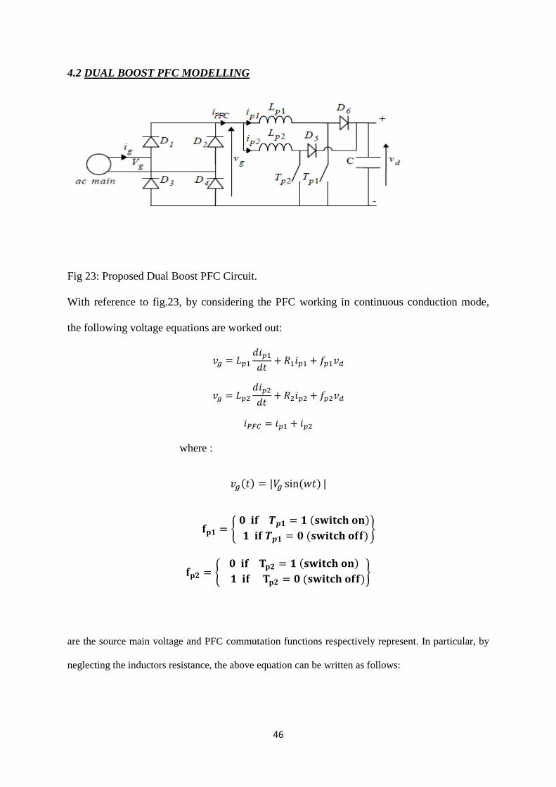
4.2 DUAL BOOST PFC MODELLING
Fig 23: Proposed Dual Boost PFC Circuit.
With reference to fig.23, by considering the PFC working in continuous conduction mode,
the following voltage equations are worked out:
where :
{
}
{
}
are the source main voltage and PFC commutation functions respectively represent. In particular, by
neglecting the inductors resistance, the above equation can be written as follows:

47
where :
because of the unidirectional ac/dc diode rectifier.
Therefore, the control of the PFC currents ip1 and ip2 can be achieved only if the following
condition occurs:
In particular if the above condition is satisfied it is possible to control the derivative of the
total PFC current iPFC :
4.3 THE CONTROL STRATEGY
The parallel connection of switch mode converter is a well-known strategy. In fig. 24 the
input currents of two interleaved PFC are shown.
The theoretically cancellation of the current iPFC ripple is possible. In particular the following
conditions have to be verified:

48
with :
where d1 and d2 the boost duty cycle respectively represents.
Unfortunately, the solutions of the above two conditions are :
and the application of the above constraints describes only an ideal working condition, fig.
25, not feasible in a real industrial application.
Fig 24: Input currents of two interleaved PFC.
Fig 25: Input currents of two interleaved PFC in ideal working condition.

49
In fig.26 the input currents of two PFC working with the proposed internal active filtering
approach are shown. Of course, by using the proposed approach, it is not possible to
completely eliminate the iPFC ripple, but a not negligible reduction is achieved.
Fig. 26: Input currents of two PFC working with the proposed internal active filtering
approach.
4.4 SIMULATION RESULTS
TWO PARALLEL BOOST CONVERTERS:
Two Boost converters working on same switching frequency are connected in parallel
supplied from the same rectified dc from ac supply mains and feeding a load.
The duty cycle of Main switch (Tp1) and Filtering switch (Tp2) are d1 and d2
respectively with condition: d2=1-d1.
The input current is found to contain fewer ripples due to the cancellation of the
current ripples of the two boost converters, that is, current quality is improved. But
the result is not much pronounced as no control strategy is used for PFC.

50
Fig 27(a): Two parallel Boost Converter- Schematic
Fig 27(b): Time Domain waveforms of inductor currents and input current

51
Fig 27(c): Input Voltage and Output Voltage waveform.
Fig 27(d): Frequency Domain Analysis of Input-Output Voltages, Inductor currents, Input
current.

52
BOOST POWER FACTOR CORRECTION CIRCUIT:
A DC-DC boost converter is used as a high-frequency active PFC circuit with a
suitable control technique, used to shape its input current and it has inherent PFC
properties. The control technique used here is a simple PI controller and a comparator
to generate the required PWM.
Although this converter operating in CICM reduces the line current harmonics, it
introduces additional losses, thus reducing the overall efficiency; it increases the
EMI, due to the high frequency content of the input current. THD is found to be
0.2119.
Fig 28(a): Boost PFC circuit- Schematic

53
Fig 28(b): Time Domain waveforms of input-output voltages, inductor currents and input
current.
Fig 28(c): Frequency Domain Analysis of Input-Output Voltages, Inductor currents, Input
current.

54
TWO PARALLEL BOOST PFC CIRCUIT:
Two boost converters are connected in parallel with same control technique used as
earlier in single boost PFC circuit, switches working with same switching frequency
and different duty cycles (phase shifting of switch conduction).As parallel connection
is used, smoothening of line current will occur and because of PFC circuit, line
current harmonics will reduce.
THD is found to be 0.0623; hence reduces substantially when parallel connection of
these two boost PFC circuit is done.
Fig 29(a): Two parallel Boost PFC circuit- Schematic

55
Fig 29(b): Time Domain waveforms of input-output voltages, inductor currents and input
current.
Fig 29(c): Frequency Domain Analysis of Input-Output Voltages, Inductor currents, Input
current.

56
4.5 STABILITY ANALYSIS
It is a well-known fact that addition of feedback loop can cause an otherwise stable system to
become unstable. Even though the transfer functions of the original converter as well as of
the loop gain contain no right half-plane poles, it is possible for the closed-loop transfer
function to contain right half-plane poles. The feedback loop then fails to regulate the system
at the desired quiescent operating point, and oscillations are mostly observed.
A Phase Margin Test is sufficient for designing most of the regulators. The phase margin is
evaluated which is given by the phase of the loop gain T calculated at the crossover
frequency and 180 degrees is added.
Where, the crossover frequency is defined as the frequency where the magnitude of the loop
gain is unity, that is
| | ⇒
If there is exactly one crossover frequency, and if the loops gain T(s) contains no right half-
plane poles, then closed loop quantities contain no right half-plane poles when the phase
margin is positive. This is an easy-to-use design tool where we simply ensure that the phase
of T is greater than -180 degrees at the crossover frequency.
But a good design should have adequate design margins, as a small phase margin causes the
closed-loop transfer functions to exhibit resonant poles with high Q in the vicinity of the
crossover frequency. The system transient response exhibits overshoot and ringing. As the
phase margin is reduced these characteristics become worse until, for , the system
becomes unstable. It is already given that for obtaining real poles (Q<0.5) requires a phase
margin of at-least 76 degrees.

57
The Bode plots of derived transfer functions of the proposed strategy:
Fig 30: Bode plot of line-to-output TF Gvg(s).
Fig 31: Bode plot of control-to-output TF Gvd(s).

58
Fig 32: Bode plot of the compensator Gc(s).
Fig 33: Bode plot of loop gain T(s) for boost PFC circuit.

59
Fig 34: Bode plot of loop gain T(s) for parallel boost PFC circuit.
As we can see the phase margin calculated for both single boost and parallel boost PFC
circuit comes positive, the systems are stable.

60
Chapter 5
EMI Filter
EMI Input Filter
Implementing EMI

61
5.1 EMI INPUT FILTER
The high-frequency ripple of the input current of switching converters generates differential-
mode EMI, while the parasitic results in common-mode EMI. Typically, the differential-
mode EMI is dominant below 2MHz, while the common-mode EMI is dominant above
2MHz.
A high-frequency active PFC stage significantly increases the differential-mode EMI,
typically by 30dB to 60dB and an EMI filter must be used to comply with EMI standards.
There are three main requirements concerning the design of the EMI filter for a PFC stage.
To discuss them, let us consider a one-stage LC filter, as shown in Fig. 5 (a).
Fig 35: One-stage LC filter for attenuating differential-mode EMI: a) Schematic; b) Phasor
diagram of line-frequency components of the system currents and voltages.
1. First requirement:
The first requirement for the EMI filter is to provide the required attenuation, in order to
ensure compliance with the EMI standards.
2. Second requirement:
Fig. 35(b) shows the phasor diagram of the line-frequency components of the system currents
and voltages. We assume that the input current ig of the PFC stage is sinusoidal and in phase
with the input voltage vg which, assuming that the voltage drop across the filter inductor La is
Diode bridge +
PFC
Vg
Zof Zic
ig
iC
Ca
La
ii
Vi
IC Ii
Ig Φ Re
Im

62
very small at line-frequency, is essentially equal to the line voltage vi . The capacitive current
IC which is proportional to Ca, introduces a displacement angle Φ between the line current Ii
and the line voltage Vi, which degrades the power factor.
This leads to the second requirement for the EMI filter: the displacement angle Φ must be
kept low. Hence, the capacitance Ca that can be used is upper limited.
Ca < Cmax,
As a consequence, the inductance La is lower limited
La > Lmin
In order to have a product LaCa that gives the required attenuation.
3. Third requirement:
The third requirement is related to the overall stability of the system. It is known that unstable
operation may occur due to the interaction between the EMI filter and the power stage. To
explain it, let us consider the thevenin equivalent circuit shown in Fig.36, of the EMI
filter/PFC stage interconnection from Fig.35 (a). Hf is the transfer function of the filter, Zof is
the output impedance of the EMI filter and Zic is the input impedance of the PFC stage.
From the equivalent circuit, we can write:
sT
sH
sZ
sZ
sH
sv
sv
f
f
ic
of
f
i
g
1
1
Zic Vg(s)
Zof
Hf.vi(s)
Fig.36 Thevenin’s equivalent
circuit

63
Where icoff ZZT can be considered as a loop gain that must satisfy the Nyquist criterion
for stability. The interaction between the EMI filter and the power converter is minimized
and no instabilities can arise in the system, if |Tf|<<1. This means that the modulus of the
output impedance of the EMI filter must be much lower than the modulus of the input
impedance of the power converter, |Zof|<<|Zic|. The aforementioned condition may be difficult
to fulfill in a PFC application. This is because, at the resonant frequency of the EMI filter, the
modulus of the output impedance Zof has a maximum that is proportional to aa CL , which
cannot be set arbitrarily low since Ca is upper limited and La is lower limited. Hence, in a
PFC application it is possible to have |Tf|>1, especially at low Zic, i.e. at low line voltage and
high load current. Therefore, if the input impedance Zic shows an excessive positive phase
shift, then icoff ZZT may not satisfy the Nyquist criterion for stability and instabilities
occur. For this reason, it is important to know the input impedance Zic of the PFC stage, in
order to be able to perform the stability analysis.

64
5.2 IMPLEMENTING EMI FILTER
BOOST PFC CIRCUIT
Fig 37(a): Boost PFC circuit with EMI filter-Schematic
Fig 37(b): Time Domain waveforms of input-output voltages, inductor currents and input
current.

65
Fig 37(c): Frequency Domain Analysis of Input-Output Voltages, Inductor currents, Input
current.
PARALLEL BOOST PFC CIRCUIT
Fig 38(a): Two parallel Boost PFC circuit with EMI filter- Schematic

66
Fig 38(b): Time Domain waveforms of input-output voltages, inductor currents and input
current.
Fig 38(c): Frequency Domain Analysis of Input-Output Voltages, Inductor currents, Input
current.

67
CONCLUSIONS
The modelling of power factor correction circuit for Boost Converter is done using a
PI controller and THD is found to be 0.2119.
When two such boost PFC circuits are connected in parallel, THD and power factor
further improves and THD came to 0.0623.
With the introduction of EMI filter at input side (LC filter), THD further reduces and
came to be 0.1084 for single boost PFC circuit and 0.022 for two parallel boost PFC
circuits.
The time domain and frequency domain analysis of input voltage and current,
inductor currents, and output voltage are done according to the modelled tuned
parameters of converters and control method.
The input current quality increases due to the filtering effect of the second boost
converter used in parallel. The switching and conduction losses also reduce.
The stability analysis of both boost PFC and dual boost PFC circuit is done and the
phase margin was found to be positive and satisfying the minimum requirement of 76
degrees for avoiding overshoot and ringing.
FUTURE SCOPE:
For further improvement, we can introduce predictive control strategy in which the
active filtering approach can be utilized so as to further reduce the current ripples and
switching losses. The switches can be made to be work under soft-switching
condition.
68
REFERENCES:
[1] Fairchild Semiconductor- “Application Note 42047,Power Factor Correction (PFC)
Basics” –www.fairchildsemi.com
[2] N. Mohan, et el. Power Electronics: Converters, Applications, and Design. New York:
NY, USA, John Wiley & Sons, Inc., 1995.
[3] R. W. Erickson, Fundamentals of power electronics. New York, NY, USA, Chapman
[4] Kurma Sai Mallika, Prof. A.K.Panda, “Topological issues in single phase power factor
correction” M.Tech thesis at National Intstitute of Technology, Rourkela. (2007).
[5] Rossetto, L., et el. “Control techniques for power factor correction converters.” University
of Padova, Via Gradenigo 6/a, 35131 Padova – ITALY. (1994): pp. 1-9.
[6] Redl, Richard, “Reducing distortion in peak-current-controlled boost power factor
correctors.” Proc. of IEEE Applied Power Electronics Conference, APEC’94. (1994): pp.
576-583.
[7] Maksimovic, Dragan, “Design of the clamped-current high-power-factor boost rectifier.”
IEEE Trans. on Industry Applications. vol. 31, no. 5, (Sept - Oct. 1995): pp. 986-992.
[8] Canesin, Carlos A., et el. “Analysis and design of constant-frequency peak-current
controlled high power-factor boost rectifier with slope compensation.” Proc. of IEEE
Applied Power Electronics Conference, APEC’96. (1996): pp. 807-813.
[9] Lai, J. S., “Design consideration for Power Factor Correction Boost converter Operating
at the Boundary of Continuous Conduction mode and Discontinuous Conduction mode.”
Proc. of IEEE Applied Power Electronics Conference, APEC’93. (1993): pp. 267-273.

69
[10] Redl, Richard, et el. “Power-Factor Correction with Interleaved Boost Converters in
Continuous-Inductor-Current Mode.” Proc. of IEEE Applied Power Electronics
Conference, APEC’93. (1993): pp.168-174.
[11] Attaianese, C.; Nardi, V.; Parillo, F.; Tomasso, G.; “ Predictive Control of Parallel Boost
Converters” in Industrial Electronics,2008, IECON 2008, 34th
Annual Conference of
IEEE.
[12] Wu, M. K. W., et el. “A review of EMI problems in switch mode power supply design.”
Journal of Electrical and Electronics Engineering, Australia. vol. 16, nos. 3&4, (1996):
pp. 193-204.
[13] Redl, Richard, “Power electronics and electromagnetic compatibility.” Proc. of IEEE
Power Electronics Specialists Conference, PESC’96. (1996): pp. 15-21.
[14] Vlatkovic, V., et el. “Input filter design for power factor correction circuits.” IEEE
Transactions on Power Electronics. vol. 11, no. 1, (Jan. 1996): pp. 199-205.
[15] Jang, Y., “Physical origins of input filter oscillations in current programmed converters.”
IEEE Transactions on Power Electronics. vol. 7, no. 4, (Oct. 1992): pp. 725-733.


![Multitrack Power Factor Correction Architectureminjie/files/multitrackpfc_slides.pdfMultilevel Boost Converter," IEEE Transactions on Power Electronics, 2015. • [Stanford TPEL18]](https://img.pdfslide.us/doc/110x75/606d4695b75a011d7207f915/multitrack-power-factor-correction-architecture-minjiefilesmultitrackpfcslidespdf.jpg)