Embed Size (px)
Citation preview
Improvement of modulation bandwidth in electroabsorption-modulated laser by utilizing
the resonance property in bonding wire
Oh Kee Kwon,1,2,*
Young Tak Han,1 Yong Soon Baek,
1 and Yun C. Chung
2
1Photonic-Wireless Convergence Components Research Department, Electronics and Telecommunications Research Institute, 138 Gajeongno, Yuseong-gu, Daejeon, South Korea
2Department of Electrical Engineering, Korea Advanced Institute of Science and Technology, 335 Gwahangno, Yuseong-gu, Daejeon 305-701, South Korea
Abstract: We present and demonstrate a simple and cost-effective technique for improving the modulation bandwidth of electroabsorption-modulated laser (EML). This technique utilizes the RF resonance caused by the EML chip (i.e., junction capacitance) and bonding wire (i.e, wire inductance). We analyze the effects of the lengths of the bonding wires on the frequency responses of EML by using an equivalent circuit model. To verify this analysis, we package a lumped EML chip on the sub-mount and measure its frequency responses. The results show that, by using the proposed technique, we can increase the modulation bandwidth of EML from ~16 GHz to ~28 GHz.
©2012 Optical Society of America
OCIS codes: (230.0230) Optical devices; (230.2090) Electro-optical devices.
References and links
1. IEEE Standard 802.3ba. 2. Y. D. Bae, B. K. Kang, B. Park, S. M. Lee, Y. H. Kim, H. K. Kim, M. K. Park, I. Kim, and D. H. Jang,
“Operation of 1550-nm electroabsorption-modulated laser at 40°C for 10-Gb/s, 40-km transmission,” IEEE J. Sel. Top. Quantum Electron. 11(1), 135–140 (2005).
3. Y. Luo, P. Cai, C. Sun, and B. Xiong, “High-speed AlGaInAs-MQW integrated EA modulator/DFB laser module based on identical epitaxial layer scheme for 40 Gb/s optic fiber communication systems,” in Proc. 19th IPRM 2007, WeB1–5 (2007).
4. C. Cole, B. Huebner, and J. E. Johnson, “Photonic integration for high-volume, low-cost applications,” IEEE Commun. Mag. 47(3), S16–S22 (2009).
5. T. Fujisawa, S. Kanazawa, N. Nunoya, H. Ishii, Y. Kawaguchi, A. Ohki, N. Fujiwara, K. Takahata, R. Iga, F. Kano, and H. Oohashi, “4×25-Gbit/s, 1.3-µm, monolithically integrated light source for 100-Gbit/s Ethernet,” in Proc. ECOC 2010, Th.9.D.1 (2010).
6. Y. H. Kwon, J. S. Choe, J. S. Sim, S. B. Kim, H. Yun, K. S. Choi, B. S. Choi, and E. S. Nam, “40 Gb/s traveling-wave electroabsorption modulator-integrated DFB lasers fabricated using selective area growth,” ETRI J. 31(6), 765–769 (2009).
7. X. Zhao, K. Hasebe, T. Sakaguchi, F. Koyama, C. J. Chang-Hasnain, N. Nishiyama, C. Caneau, and C. E. Zah, “Tunable optical equalizer using diffraction grating filters,” IEEE Photon. Technol. Lett. 20(18), 1590–1592 (2008).
8. T. Hatta, T. Miyahara, M. Ishizaki, N. Okada, S. Zaizen, K. Motoshima, and K. Kasahara, “Inductance-controlled electroabsorption modulator modules using the flip-chip bonding technique,” J. Lightwave Technol. 23(2), 582–587 (2005).
9. Y. Wang, Y. Cheng, F. Zhou, H. Zhu, L. Zhao, and W. Wang, “Design of high frequency compensation submount for 40Gbit/s lumped electroabsorption modulated lasers,” in Proc. OSA/ACP 2009, WL38 (2009).
10. G. L. Li, C. K. Sun, S. A. Pappert, W. X. Chen, and P. K. L. Yu, “Ultra-speed traveling-wave electroabsorption modulator-design and analysis,” IEEE Trans. Microw. Theory Tech. 47(7), 1177–1183 (1999).
11. H. Fukano, Y. Akage, Y. Kawaguchi, Y. Suzaki, K. Kishi, T. Yamanaka, Y. Kondo, and H. Yasaka, “Low chirp operation of 40 Gbit/s electroabsorption modulator integrated DFB laser module with low driving voltage,” IEEE J. Sel. Top. Quantum Electron. 13(5), 1129–1134 (2007).
1. Introduction
Due to the ever-increasing data traffic in the fiber-optic network, there have been many efforts to develop high-speed light sources [1–6]. These light sources should also be compact,
#158426 - $15.00 USD Received 21 Nov 2011; revised 9 Jan 2012; accepted 9 Jan 2012; published 10 May 2012(C) 2012 OSA 21 May 2012 / Vol. 20, No. 11 / OPTICS EXPRESS 11806
reliable, and cost-effective, and have superior performances such as the low chirp and low power consumption. It has been considered that the electro-absorption-modulated laser (EML) can satisfy all these requirements, thus is suitable for the use in the high-speed applications operating at 25 Gb/s or 40 Gb/s [3–6]. However, the modulation bandwidth of the EML is often limited by the RC time constant resulting from its junction capacitance. To overcome this problem, it is necessary to modify the structural parameters of the electro-absorption modulator (EAM). However, it is usually difficult to increase the modulation bandwidth without compromising other important parameters such as the extinction ratio, insertion loss, and required driving voltage.
There are several techniques commonly used to avoid these performance compromises [6–9]. For example, it has been demonstrated that the modulation bandwidth of the EML can be increased, without sacrificing other performances, by introducing the travelling-wave (TW) electrode to the EAM [6]. However, this technique requires complicated fabrication processes and stringent process tolerances. The modulation bandwidth of the EML can also be extended by utilizing the equalization technique based on the optical filter [7]. However, in spite of its excellent capability of enhancing the modulation bandwidth (e.g., from 10 to 45 GHz), this technique is problematic since it not only requires a large number of additional components and precise optical alignment, but also suffers from large excess loss.
Previously, it has also been reported that the modulation bandwidth of EAM can be improved by using the flip-chip bonding technique and controlling the inductance of the bonding lead between the EAM chip and load impedance [8]. However, when this flip-chip bonding technique applied to the EML, it can suffer from the difficulty of heat dissipation of distributed feedback laser diode (DFB LD) and the effect of RF parasitics of ceramic (or Si) sub-mount, and can require an additional alignment pattern for the chip (boned to the sub-mount in the form of p-side down). Another technique proposed to increase the modulation bandwidth of EML is using the RF resonance caused by placing a T-resonator (i.e., shunt open circuit stub) between the lumped EML chip and the load impedance on the sub-mount. Thus, the frequency response of the EML can be changed by the length of the stub [9]. This technique appears to be attractive since it can increase the modulation bandwidth of the EML without degrading other performances including the excess loss, and has a simple configuration. Previously, it has been shown that this technique can increase the modulation bandwidth of EML by only 2 GHz using a numerical simulation. No experimental data supporting this simulation result has yet been reported.
In this paper, we propose and demonstrate a simple and cost-effective technique for improving the modulation bandwidth of EML. This is based on the wire-bonding technique (widely used for most commercial transmitted optical subassembly (TOSA)) and utilizes the RF resonance generated by the junction capacitance of the EAM and the inductances of the bonding wires on its sub-mount. Compared to the flip-chip bonding technique, this technique offers sufficient heat-dissipation of the EML and has good immunity to the RF parasitics of sub-mount. Besides, there is no significant constraint to the geometry of the device and sub-mount (i.e., high degree of freedom) in doing the wire-bonding and no need to use expensive AuSn solder which is usually used for flip-chip bonding (i.e., cost-effective). The frequency response of the EML can be compensated simply by adjusting the lengths of bonding wires or by using the different types of bonding wire (i.e., simple configuration). To evaluate the effectiveness of the proposed technique, we package an EML chip on the sub-mount and investigate the effect of this inductance modification (caused by adjusting the lengths of the bonding wires between the RF feeding line and EML chip and also between the EML chip and load impedance) on its frequency responses.
The rest of this paper is organized as follows. The circuit model and simulation results are described in Section II; Section III presents the experimental results obtained by using the proposed technique. Finally, Section IV concludes the paper.
#158426 - $15.00 USD Received 21 Nov 2011; revised 9 Jan 2012; accepted 9 Jan 2012; published 10 May 2012(C) 2012 OSA 21 May 2012 / Vol. 20, No. 11 / OPTICS EXPRESS 11807
2. Circuit model and simulation results
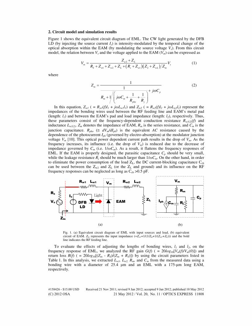
Figure 1 shows the equivalent circuit diagram of EML. The CW light generated by the DFB LD (by injecting the source current Is) is intensity-modulated by the temporal change of the optical absorption within the EAM (by modulating the source voltage Vs). From this circuit model, the relation between Vs and the voltage applied to the EAM (Vm) can be expressed as
( )( )2
1 2 1 2
w L
m s
S w w L s w wL m
Z ZV V
R Z Z Z R Z Z Z Z
+=
+ + + + + + (1)
where
1
1
1 11
m
p
m m
pho j
Z
j C
R j CR R
ω
ω
=+
+ + +
(2)
In this equation, Zw1 ( = Rw1(f)l1 + jωLw1l1) and Zw2 ( = Rw2(f)l2 + jωLw2l2) represent the impedances of the bonding wires used between the RF feeding line and EAM’s metal pad (length: l1) and between the EAM’s pad and load impedance (length: l2), respectively. Thus, these parameters consist of the frequency-dependent conduction resistance Rw1(2)(f) and inductance Lw1(2). Zm denotes the impedance of EAM, Rm is the series resistance, and Cm is the
junction capacitance. Rpho (≅ dVm/dIph) is the equivalent AC resistance caused by the dependence of the photocurrent Iph (governed by electro-absorption) at the modulator junction voltage Vm [10]. This optical power dependent current path results in the drop of Vm. As the frequency increases, its influence (i.e. the drop of Vm) is reduced due to the decrease of impedance governed by Cm (i.e. 1/ωCm). As a result, it flattens the frequency responses of EML. If the EAM is properly designed, the parasitic capacitance Cp should be very small, while the leakage resistance Rj should be much larger than 1/ωCm. On the other hand, in order to eliminate the power consumption of the load ZL, the DC current-blocking capacitance Ccb can be used between the Zw2 and ZL (or the ZL and ground) and its influence on the RF frequency responses can be neglected as long as Ccb >0.5 pF.
Vm
Rm
IphCp
RjCmVs
Rs
ZLEAM
Is
DFB
LD
VmLw2Rw1 Lw1 Rw2
Zin
Light
(a) (b)
Fig. 1. (a) Equivalent circuit diagram of EML with input sources and load, (b) equivalent circuit of EAM. Zin represents the input impedance (=Zw1+1/(1/Zm+1/(Zw2+ZL))) and the bold line indicates the RF feeding line.
To evaluate the effects of adjusting the lengths of bonding wires, l1 and l2, on the frequency response of EML, we analyzed the RF gain G(f) ( = 20log10[Vm(f)/Vm(0)]) and return loss R(f) ( = 20log10[(Zin - RS)/(Zin + RS)]) by using the circuit parameters listed in Table 1. In this analysis, we extracted Lw1, Lw2, Rm, and Cm from the measured data using a bonding wire with a diameter of 25.4 µm and an EML with a 175-µm long EAM, respectively.
#158426 - $15.00 USD Received 21 Nov 2011; revised 9 Jan 2012; accepted 9 Jan 2012; published 10 May 2012(C) 2012 OSA 21 May 2012 / Vol. 20, No. 11 / OPTICS EXPRESS 11808
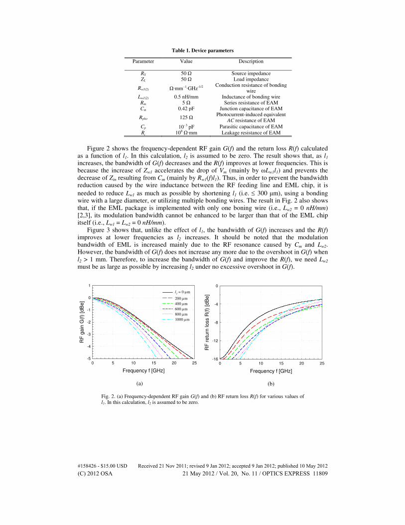
Table 1. Device parameters
Parameter
Value
Description
RS 50 Ω Source impedance ZL 50 Ω Load impedance
Rw1(2) Ω·mm−1·GHz-1/2 Conduction resistance of bonding
wire Lw1(2) 0.5 nH/mm Inductance of bonding wire Rm 5 Ω Series resistance of EAM Cm 0.42 pF Junction capacitance of EAM
Rpho 125 Ω Photocurrent-induced equivalent
AC resistance of EAM
Cp 10−3 pF Parasitic capacitance of EAM
Rj 108 Ω·mm Leakage resistance of EAM
Figure 2 shows the frequency-dependent RF gain G(f) and the return loss R(f) calculated as a function of l1. In this calculation, l2 is assumed to be zero. The result shows that, as l1 increases, the bandwidth of G(f) decreases and the R(f) improves at lower frequencies. This is because the increase of Zw1 accelerates the drop of Vm (mainly by ωLw1l1) and prevents the decrease of Zin resulting from Cm (mainly by Rw1(f)l1). Thus, in order to prevent the bandwidth reduction caused by the wire inductance between the RF feeding line and EML chip, it is
needed to reduce Lw1 as much as possible by shortening l1 (i.e. ≤ 300 µm), using a bonding wire with a large diameter, or utilizing multiple bonding wires. The result in Fig. 2 also shows that, if the EML package is implemented with only one boning wire (i.e., Lw2 = 0 nH/mm) [2,3], its modulation bandwidth cannot be enhanced to be larger than that of the EML chip itself (i.e., Lw1 = Lw2 = 0 nH/mm).
Figure 3 shows that, unlike the effect of l1, the bandwidth of G(f) increases and the R(f) improves at lower frequencies as l2 increases. It should be noted that the modulation bandwidth of EML is increased mainly due to the RF resonance caused by Cm and Lw2. However, the bandwidth of G(f) does not increase any more due to the overshoot in G(f) when l2 > 1 mm. Therefore, to increase the bandwidth of G(f) and improve the R(f), we need Lw2 must be as large as possible by increasing l2 under no excessive overshoot in G(f).
Frequency f [GHz]
0 5 10 15 20 25
RF
ga
in G
(f)
[dB
e]
-5
-4
-3
-2
-1
0
1
l1 = 0 µm
200 µm
400 µm
600 µm
800 µm
1000 µm
Frequency f [GHz]
0 5 10 15 20 25
RF
retu
rn loss R
(f)
[dB
e]
-16
-12
-8
-4
0
(a) (b)
Fig. 2. (a) Frequency-dependent RF gain G(f) and (b) RF return loss R(f) for various values of l1. In this calculation, l2 is assumed to be zero.
#158426 - $15.00 USD Received 21 Nov 2011; revised 9 Jan 2012; accepted 9 Jan 2012; published 10 May 2012(C) 2012 OSA 21 May 2012 / Vol. 20, No. 11 / OPTICS EXPRESS 11809
Frequency f [GHz]
0 5 10 15 20 25
RF
gain
G(f
) [d
Be
]
-5
-4
-3
-2
-1
0
1
l2 = 0 µm
200 µm
400 µm
600 µm
800 µm
1000 µm
Frequency f [GHz]
0 5 10 15 20 25
RF
re
turn
lo
ss R
(f)
[dB
e]
-16
-12
-8
-4
0
(a) (b)
Fig. 3. (a) Frequency-dependent RF gain G(f) and (b) RF return loss R(f) for various values of l2. In this calculation, l1 is assumed to be zero.
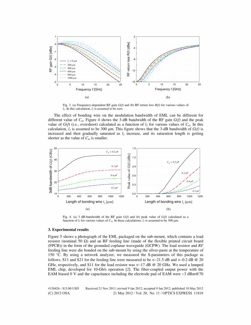
The effect of bonding wire on the modulation bandwidth of EML can be different for different value of Cm. Figure 4 shows the 3-dB bandwidth of the RF gain G(f) and the peak value of G(f) (i.e., overshoot) calculated as a function of l2 for various values of Cm. In this calculation, l1 is assumed to be 300 µm. This figure shows that the 3-dB bandwidth of G(f) is increased and then gradually saturated as l2 increase, and its saturation length is getting shorter as the value of Cm is smaller.
Length of bonding wire l2 [µm]
0 200 400 600 800 1000 1200
3d
B-b
andw
idth
of
G(f
) [G
Hz]
10
20
30
40
50
Cm = 0.2 pF
0.3 pF
0.4 pF
0.5 pF
Length of bonding wire l2 [µm]
0 200 400 600 800 1000 1200
Pea
k v
alue
of
G(f
) [d
Be]
0.0
0.3
0.6
0.9
1.2
1.5
Cm = 0.2 pF
0.3 pF
0.4 pF
0.5 pF
(a) (b)
Fig. 4. (a) 3 dB-bandwidth of the RF gain G(f) and (b) peak value of G(f) calculated as a function of l2 for various values of Cm. In these calculations, l1 is assumed to be 300 µm.
3. Experimental results
Figure 5 shows a photograph of the EML packaged on the sub-mount, which contains a load resistor (nominal 50 Ω) and an RF feeding line (made of the flexible printed circuit board (FPCB)) in the form of the grounded coplanar waveguide (GCPW). The load resistor and RF feeding line were die bonded on the sub-mount by using the silver-paste at the temperature of 150 °C. By using a network analyzer, we measured the S-parameters of this package as
follows. S11 and S21 for the feeding line were measured to be <−21.5 dB and >−0.2 dB @ 20
GHz, respectively, and S11 for the load resistor was <−17 dB @ 20 GHz. We used a lumped EML chip, developed for 10-Gb/s operation [2]. The fiber-coupled output power with the EAM biased 0 V and the capacitance including the electrode pad of EAM were ~3 dBm@70
#158426 - $15.00 USD Received 21 Nov 2011; revised 9 Jan 2012; accepted 9 Jan 2012; published 10 May 2012(C) 2012 OSA 21 May 2012 / Vol. 20, No. 11 / OPTICS EXPRESS 11810
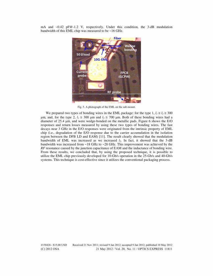
mA and ~0.42 [email protected] V, respectively. Under this condition, the 3-dB modulation bandwidth of this EML chip was measured to be ~16 GHz.
50ΩΩΩΩload
FPCB(GCPW)
RF probe
10G-EML
Wedge bonding
Currentprobe
Fiber
Fig. 5. A photograph of the EML on the sub-mount.
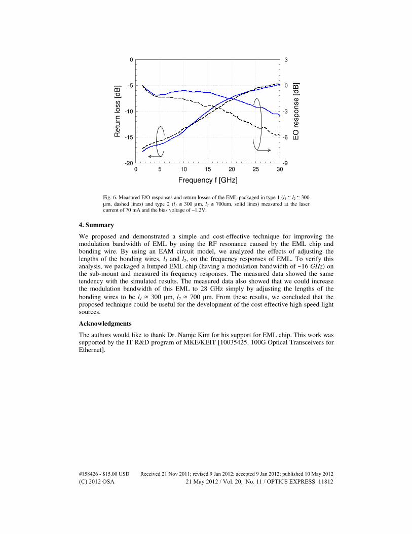
We prepared two types of bonding wires in the EML package: for the type 1, l1 ≅ l2 ≅ 300
µm, and, for the type 2, l1 ≅ 300 µm and l2 ≅ 700 µm. Both of these bonding wires had a diameter of 25.4 µm, and were wedge-bonded on the metallic pads. Figure 6 shows the E/O responses and return losses measured by using these two types of bonding wires. The fast decays near 3 GHz in the E/O responses were originated from the intrinsic property of EML chip (i.e., degradation of the E/O response due to the carrier accumulation in the isolation region between the DFB LD and EAM) [11]. The result clearly showed that the modulation bandwidth of EML was increased as we increased l2. In fact, it showed that the 3-dB bandwidth was increased from ~18 GHz to ~28 GHz. This improvement was achieved by the RF resonance caused by the junction capacitance of EAM and the inductance of bonding wire. From these results, we concluded that, by using the proposed technique, it is possible to utilize the EML chip previously developed for 10-Gb/s operation in the 25-Gb/s and 40-Gb/s systems. This technique is cost-effective since it utilizes the conventional packaging process.
#158426 - $15.00 USD Received 21 Nov 2011; revised 9 Jan 2012; accepted 9 Jan 2012; published 10 May 2012(C) 2012 OSA 21 May 2012 / Vol. 20, No. 11 / OPTICS EXPRESS 11811
Frequency f [GHz]
0 5 10 15 20 25 30
Re
turn
loss [d
B]
-20
-15
-10
-5
0
EO
re
sponse
[d
B]
-9
-6
-3
0
3
Fig. 6. Measured E/O responses and return losses of the EML packaged in type 1 (l1 ≅ l2 ≅ 300
µm, dashed lines) and type 2 (l1 ≅ 300 µm, l2 ≅ 700um, solid lines) measured at the laser current of 70 mA and the bias voltage of –1.2V.
4. Summary
We proposed and demonstrated a simple and cost-effective technique for improving the modulation bandwidth of EML by using the RF resonance caused by the EML chip and bonding wire. By using an EAM circuit model, we analyzed the effects of adjusting the lengths of the bonding wires, l1 and l2, on the frequency responses of EML. To verify this analysis, we packaged a lumped EML chip (having a modulation bandwidth of ~16 GHz) on the sub-mount and measured its frequency responses. The measured data showed the same tendency with the simulated results. The measured data also showed that we could increase the modulation bandwidth of this EML to 28 GHz simply by adjusting the lengths of the
bonding wires to be l1 ≅ 300 µm, l2 ≅ 700 µm. From these results, we concluded that the proposed technique could be useful for the development of the cost-effective high-speed light sources.
Acknowledgments
The authors would like to thank Dr. Namje Kim for his support for EML chip. This work was supported by the IT R&D program of MKE/KEIT [10035425, 100G Optical Transceivers for Ethernet].
#158426 - $15.00 USD Received 21 Nov 2011; revised 9 Jan 2012; accepted 9 Jan 2012; published 10 May 2012(C) 2012 OSA 21 May 2012 / Vol. 20, No. 11 / OPTICS EXPRESS 11812