Embed Size (px)
Citation preview
Advance in Electronic and Electric Engineering. ISSN 2231-1297, Volume 3, Number 9 (2013), pp. 1121-1134 © Research India Publications http://www.ripublication.com/aeee.htm
Improved NAND Flash Memories Storage Reliablity Using Nonlinear Multi Error Correction Codes
E. Ramakrishna Naik* and L.S. Devaraj** *M.Tech(VLSI), Dept. of ECE, Intellectual Institute Of Technology, Anantapur.
Assistant professor Dept. of ECE, Intellectual Institute Of Technolog, Anantapur. E-mail: *[email protected], **[email protected]
Abstract
Multi-level cell (MLC) NAND flash memories are popular storage media because of their power efficiency and large storage density. Conventional reliable MLC NAND flash memories based on BCH codes or Reed-Solomon (RS) codes have a large number of undetectable and miscorrected errors. Moreover, standard decoders for BCH and RS codes cannot be easily modified to correct errors beyond their error correcting capability t = [d-1/2] , where d is the Hamming distance of the code. In this paper, we propose two general constructions of nonlinear multi-error correcting codes based on concatenations or generalized from Vasil’ev codes. The proposed constructions can generate nonlinear bit-error correcting or digit-error correcting codes with very few or even no errors undetected or miscorrected for all codewords. Moreover, codes generated by the generalized Vasil’ev construction can correct some errors with multiplicities larger than t without any extra overhead in area, latency, and power consumption compared to schemes where only errors with multiplicity up to t are corrected. The design of reliable MLC NAND flash architectures can be based on the proposed nonlinear multi-error correcting codes. The reliability, area overhead and the penalty in latency and power consumption of the architectures based on the proposed codes are compared to architectures based on BCH codes and RS codes. The results show that using the proposed nonlinear error correcting codes for the protection of MLC NAND flash memories can reduce the number of errors undetected or miscorrected for all codewords to be almost 0 at the cost of less than 20% increase in
E. Ramakrishna Naik & L.S. Devaraj
1122
power and area compared to architectures based on BCH codes and RS codes. Index Terms: Multi-error correcting codes, nonlinear codes, re-liable memory.
1. Introduction The semiconductor industry has witnessed an explosive growth of the NAND flash memory market in the past several decades. Due to its high data transfer rate, low power consumption, large storage density and long mechanical durability, the NAND flash memories are widely used as storage media for devices such as portable media players, digital cameras, cell phones, and low-end netbooks.
The increase of the storage density and the reduction of the cost per bit of flash memories were traditionally achieved by the aggressive scaling of the memory cell transistor until the multi-level cell (MLC) technology was developed and implemented in 1997. MLC technology is based on the ability to precisely control the amount of charge stored into the floating gate of the memory cell for he purpose of setting the threshold voltage to a number of different levels corresponding to different logic values, which enables the storage of multiple bits per cell.
However, the increased number of programming threshold voltage levels has a negative impact on the reliability of the device due to the reduced operational margin. The raw bit error rate of the MLC NAND flash memory is around 10 and is at least two orders of magnitude worse than that of the single level cell (SLC) NAND flash memory . Moreover, the same reliability concerns as for SLC NAND flash memories, e.g., program/read disturb, data retention, programming/erasing endurance, and soft errors [may become more significant for MLC NAND flash memories.
Hence a powerful error correcting code (ECC) that is able to correct at least 4-bit errors is required for the MLC NAND flash memories to achieve an acceptable application bit error rate, which is no larger than 10 .
Several works have investigated the use of linear block codes to improve the reliability of MLC NAND flash memories. In, the authors presented a high-throughput and low-power ECC
NAND flash memory chip incorporating a 250 MHz BCH error correcting
architecture was shown. The author of demon-strated that the use of strong BCH codes (e.g., 12,15,67,102) can effectively increase the number of bits/cell thus further in-creasing the storage capacity of MLC NAND flash memories. In , an adaptive-rate ECC architecture based on BCH codes was proposed. The design had four operation modes with dif-ferent error correcting capabilities. An ECC architecture based on
Imp
Ree
equfor basebasecan
2. Mulvoltsatis
a nuareaoverin thbytebytereducritioverflex
flashretefor progprefmembursrandthe
3. Thefunc
proved NAN
ed-Solomon was pro
al to four. Tthe encodered on BCHed on asymcorrect all a MLC NAlti-level celtage level osfies a GausThe data of
umber of paa are phys-icrhead functhe total numes. More spes for 4096undant bits ical as for rhead is m
xible design Similar to Sh memorie
ention, progSLC flash
gram disturferred symmmories are mstiness or ldom symmeerror vector Construc
e error detections. The
ND Flash Me
n (RS) codesoposed in , The architecr and the d
H codes witmmetric limasymmetric
AND Flashll is able tof the cell. Inssian distribf the NANDages. Each pcally the sations such amber of bytepare bytes m6 data byteof the errorother typesostly determof more po
SLC flash mes include gram-ming/e
memories rb and data metry . Mormore likelylocal data detric error mr. The distor
ctions of Necting propnonlinearity
Memories Sto
s of length 8which can
cture achievdecoder but th the same
mited-magnitc errors of m
h Memoro store muln practice, t
bution due toD flash mempage stores me as cells
as ECC and es per pagemay be reqes . Due tor correctings of memormined by thwerful error
memories, ththreshold verasing endua lot of erretention , reover, exp
y to occur udependencymodel. Let rted output
Nonlinearperties of ny of a fun
orage Reliab
828 and 820n correct all ves higher th
needs 32 me error corrtude error c
mul-tiplicitie
ies ltiple bits bthe thresholo random m
mory is organ data byte
in the rest wear-leveli is usually 3
quired as theo the exist
g codes usedries such ashe number r correctinghe primary voltage disturance, andrrors are asfor MLC N
perimental runiformly wy. Thereby,
be the erro
r Multi-Ernonlinear conction
blity Using
0 informatiobit errors o
hroughput, rmore redundecting capacorrecting ces up to .
by preciselyld voltage o
manufacturinnized in bloes and spaof the page ing . The pr3%, e.g., 64e page sizetence of spd for NANDs SRAM anof redunda
g codes for Nfailure mectribution, pd single evesymmetric, NAND flashresults showwithin a pag
throughoutor-free outp
rror Corrodes are hi
Nonlinear M
on digits conof multiplicrequires lesdant bits thaability. In , code was p
y controllinof the wholeng variationocks. Each bare bytes. Cand are typ
roportion of4 spare bytee increases, pare bytes, D flash memnd DRAM ant bits. ThNAND flashcha-nisms foprogram/reaent upset. He.g., errors
h memoriesw that errorsge without t this pape
put of the m
recting Coighly relate
can be
Multi 1
nstructed ovcity less thass area overhan architectan architec
proposed, w
ng the threse memory as .
block consisCells in the spi-cally usedf the spare bes for 2048 e.g., 218 sthe numbe
mories is nowhere the
his allows fh memoriesor MLC NA
ad disturb, However, ws introduceds errors havs in MLC fany observr we assum
memory and
odes ed to nonlidefined
1123
ver an or head tures cture
which
shold array
sts of spare d for bytes data
spare er of ot as area
for a .
AND data
while d by
ve no flash vable me a
be
inear
112
valunon
3.1 Thecon
T
Let
not
cod
24
where ue of isnlinear funct
Multi-Erro
e first constrcatenating l
Table I: Out
Theorem 1:
on-zero erro
. Proof: Let
, The error m If andbe satisfiedAlgorithm es in theoreInput : C¯=Output : e=
denotes s, the hightion when
or Correctiruction of nlinear and n
tput of the D
: Let be a line
or will be d
b
, a
masking equ
d , ared. The error
1: Error Coem1: =(x1¯,x2¯,x3=(e1,e2,e3),E
the probabiher the corr
.
ing Codes Bnonlinear muonlinear red
Decoder for
ear code wi is the enco
etected with
be the error
and
uations can b
e not both 0will alwaysorrecting A
3¯) ERR
ility of occresponding
Based on Culti-error codundant dig
r Linear Cod
be a noith Hamminoding functi
h a probabil
r vector, wh
.
be written a
0, at least ons be detected
Algorithm fo
E. Ramakr
currence of nonlinearit
Concatenatiorrecting coits.
des that Can
onlinear funng distanceion. The cod
lity of at lea
ere
as
ne of the eqd. or the nonlin
rishna Naik
event . Tty of is.
ions odes is based
n Correct Up
nction with , where
de defined b
ast
quations sh
near multi-
& L.S. Dev
The smaller is a per
d on the ide
p to T Error
nonlinearit
by
own above
error correc
varaj
r the rfect
ea of
rs.
ty . and
will
cting
Imp
4.
In thnonconBCH 4.1 Thelinestruneedthe
is
propmuldetacorrpara
proved NAN
1. begin 2. Decode3. If Ev =04. No erro5. else if E6. Uncorre7. else if E8. Uncorre9. else 10. Ev >0; 11. If e¯1=012. Error in13. ERR=014. Else 15. Comput16. Comput17. If ŝ=0 th18. e=(e1,e19. else 20. Uncorre21. ERR=1 HardwarMulti-Erhis section,
nlinear multisumption ofH codes and
Encoder Ae encoder foear feedbackuctures for Lds clock computationthe numberCompared posed nonlltiplier and ailed architrecting codeallel LFSR p
ND Flash Me
e V, comput0 ,S=0 then
ors are detecEv =0 ,S≠0 tecteble multEv =-1 then ecteble mult
0 then n the redund0;
te x1¯= x1¯te ŝ=f(x1¯) hen 2,e3), ERR=
ecteble mult
re Design rror Corre
we presenti-error corref the proposd RS codes
Architectureor BCH codk shift regiLFSRs are wcycles whiln of the redr of informato the encolinear multtwo registe
tecture of te generated proposed in
Memories Sto
te S;
cted ,ERR=0then ti-errors are
ti-errors are
dant digits a
¯ e1¯, x2¯ =x2¯;
=0;
ti-errors are
of the Enecting Cot the encodeecting codessed architec(see Section
e des and RS cister (LFSRwell studiedle the paralldundant bits ation bits anoder for theti-error corers for the cthe encodeby Theorem
n [26]. The p
orage Reliab
0;
e detected ,E
e detected ,E
are detected
= x2¯ e2¯;
e detected ,
ncoder anodes er and the ds. We estimctures and con V).
codes are coR) architectd in the comlel LFSR nat the cost
nd is the pa e BCH coderrecting cocomputationr for the n
m 3 is showparallelism
blity Using
ERR=1;
ERR=1;
,
d the Dec
decoder archmate the area
ompare them
onventionalure. Both tmmunity. Ineeds only of higher haarallelism lees and RS des require
n of the nonnonlinear (
wn in Fig. 2. level of the
Nonlinear M
coder for
hi-tectures fa, the latencym to archite
ly implemethe serial an general, t
clock ardware comevel of the Lcodes, the es one monlinear redu(8281,8201,The design
e design is 1
Multi 1
Nonlinea
for the propy and the poectures base
ented based and the parthe serial Lcycles to fimplexity, wLFSRs. encoder for
ore finite undant bits. 11) 5-bit e
n is based on10. During
1125
ar
osed ower ed on
on a rallel
LFSR inish
where
r the field The
error n the each
E. Ramakrishna Naik & L.S. Devaraj
1126
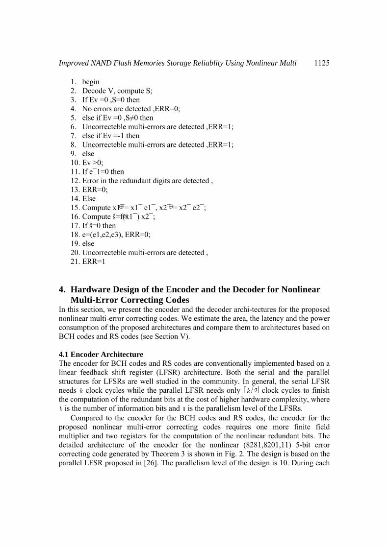
clock cycle, 10 information bits are inputted to the encoder. The most significant bit of the message is input via a separate port. The first information bit for the BCH
code is derived by XORing with the first bit of at the first clock cycle (when as shown in the figure). The bottom half of the architecture is a parallel LFSR
used to generate the redundant bits for BCH codes. is a 10 70 binary matrix . During each clock cycle, the 10 most significant bits in the shift register are XORed with the new input and then multiplied by . The output of the multiplier is XORed with the shifted data from the shift register to generate the input to the register. The top half of the architecture is for the computation of nonlinear redundant bits. During the even-numbered clock cycles, the 10-bit input is buffered. During the odd-numbered clock cycles, the buffered data is multiplied by the new input in and then added to the output registers. A 10-bit mask is XORed with the data in the output register to generate the nonlinear redundant bits. For the (8281,8201,11) 5-error-correcting code, 820 clock cy-cles are required to complete the encoding of the message.
The encoder for the (8280,8200,11) nonlinear 5-bit error correcting code based on Theorem 1 is similar to the one shown
Fig. 2: Architecture of the encoder for the (8281,8201,11) nonlinear 5-error-
correcting code.in Fig. 2. The same structure (top half) is used to compute the 10-bit nonlinear redundant bits. The main difference be-tween the two encoders is as follows. First, the encoder for the (8280,8200,11) code does not require a separate port for . All information bits are input via in 820 clock cycles, assuming a parallelism level of 10. Second, the encoding of the (8280,8200,11) code needs one more clock cycle to complete compared to the (8281,8201,11) code. At the 821th clock cycle, the input to (Fig. 2) is switched to the already-generated nonlinear check bits using a 10-bit 2:1 multiplexer.The former, however, requires that all operations are performed in
.
Imp
B. DThedecomaipolythe erroand corr
is a
Henbe throcloc
foneed
erroalgostudmin
genneed
of th
per co
conarcherro
proved NAN
Decoder Are decoding oding of a inly containynomial genBCH codes
or magnitudthen prese
recting code1) Syndromnarrow-sen. For a
, where nce only oddcomputed u
oughput of tck cycle. Figor one . ded. Error Loca
or locator porithm. Thedied in the cnimize the ar
anerated in ded for the gChien Sear
byhe error loc as
The compu
clock cycleontains -stant and hitecture is or locator po
ND Flash Me
rchitecture of the propBCH code
ns three paneration blos, the decodde. We next ent the deces.
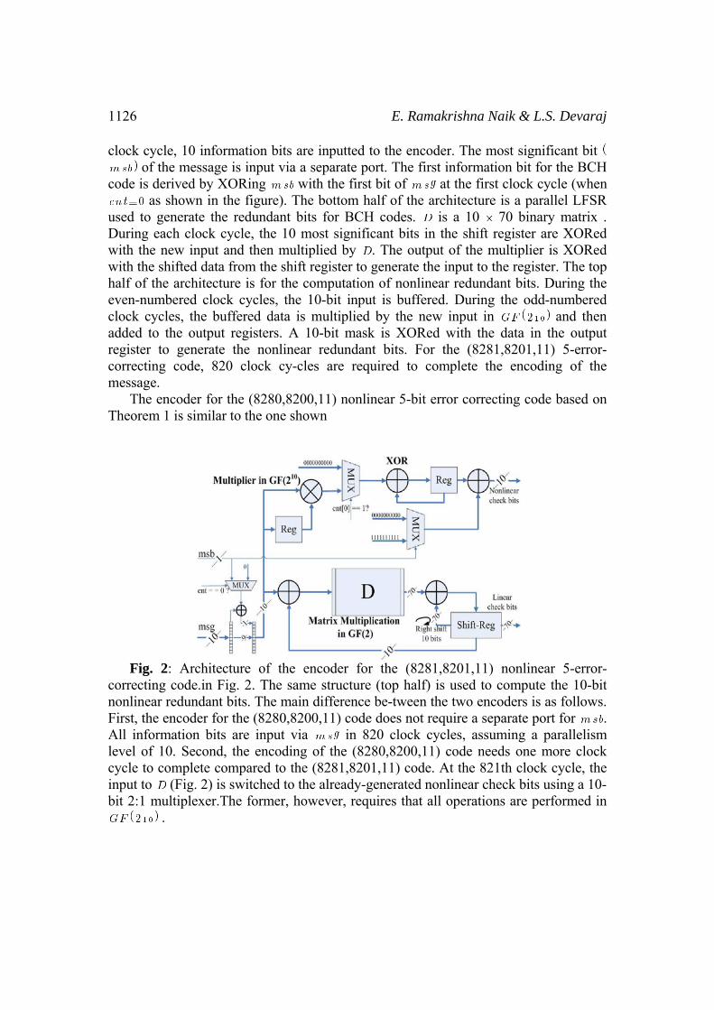
me Computanse BCH co
-
is the primd-numberedusing a muthe decoder,g. 3 shows tFor the w
ator Polynopolynomial e hardwarecommunity rea overheand two FIF
clogeneration o
rch: Let us dy . The Chcator polyno
utation comp. T
e. A typical -bit multipl adders inproposed. Tolynomial,
Memories Sto
posed nonle or a RS carts: the sy
ock and the der for the R
briefly disccoder archi
ation: Withoode . Let us -error-correc
mitive elemend needs tuch simple, a parallel dthe syn-drom
whole syndr
omial Gener will be
implemen. In our des
ad. The desigFOs. The eock cycles.of . denote the phien search omial . If
plexity is reThe algorithm
imple-mentexers and r
n The authorsmost of the
orage Reliab
linear multicode. The syndrome cChien searc
RS codes recuss the impitecture for
out loss of gdenote the rcting BCH
nt of to be compuer square cdesign can bme computarome compu
ration: Afte generated
ntations of sign a fully gn mainly r
error locato. For our d
primitive ele algorithm e
, th
duced based m can also btation of theregisters, . In , a strs showed the Galois fie
blity Using
i-error cor-rstandard deomputationch block. Coquires one mplementatior the propo
generality, areceived cocodes, the
. For binuted from ircuit in be applied tation circuitutation blo
er the syn-using the
the BM alserial struc
requires threor polynomidesign,
ement in exhaustivelyhe error loca
d on the facbe paral-lelee algorithm
multiplierength-reduhat by a simeld multiplic
Nonlinear M
recting codecoder for tn block, thompared to more block
on of the abosed nonlin
as-sume thaodeword by
syn-dromes
nary BCH c. The other
. Tto process mt with a parack, such
dromes areBerlekamp
lgorithms hcture proposee multiplierial of de and 20 cl
y tests whetation is
t that ed to test muwith a para
ers for multuced parallemple transfocations can
Multi 1
des requiresthe BCH ce error locthe decode
k to computeove four bl
near multi-e
at the BCH c
s are define
codes, r syndromesTo improvemultiple bitsallelism lev
struc-tures
e computed,p-Massey (Bhave been sed in is users in egree canlock cycles
ther is a . Rewri
ultiple positallelism levti-plication bel Chien seformation of
be replaced
1127
s the odes cator er for e the ocks error
code
ed as
. s can e the s per el of
s are
, the BM) well
ed to
n be s are
root ite
tions el of by a
earch f the d by
112
shifdeta
polypoly
Fornis thsumcom
decosimibe cFirssyndrecolinethe mis
F
slighexambit e167and BCH
28
ft operationail of the arc4) Error Mynomial , ynomial
where ney’s algorihe derivativ
m of the termpu-tation o
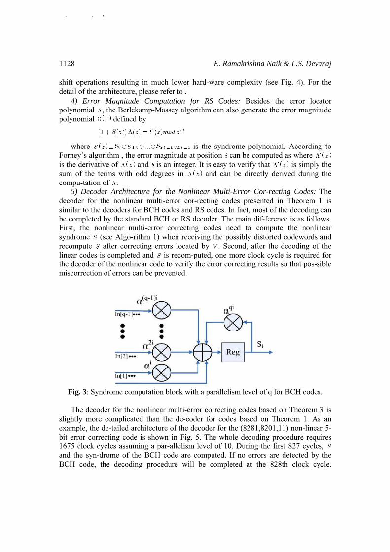
5) Decoderoder for thilar to the dcompleted bst, the nondrome (sompute aear codes is decoder of correction o
Fig. 3: Synd The decodehtly more cmple, the deerror correc5 clock cycthe syn-dr
H code, th
s resulting chitecture, pMagnitude the Berleka
defined b
ithm , the erve of anrms with odof . r Architectu
he nonlineardecoders forby the standnlinear multee Algo-rith
after correctcompleted the nonline
of errors can
drome comp
er for the nocomplicatede-tailed archcting code icles assuminrome of thehe decoding
in much loplease refer
Computatiamp-Masseyby
rror magnitund is an indd degrees
ure for the r multi-error BCH codedard BCH orti-error corhm 1) whenting errors land is re
ear code to vn be prevent
putation bloc
onlinear mud than the dhitecture ofis shown inng a par-all
e BCH codeg procedure
ower hard-wto . ion for RSy algorithm
is the
ude at positnteger. It is in an
Nonlinear or cor-rectins and RS cor RS decoderrecting codn receiving located by
ecom-puted,verify the erted.
ck with a pa
ulti-error code-coder fof the decoden Fig. 5. Thlelism levele are compue will be c
E. Ramakr
ware compl
S Codes: Bcan also ge
syndrome tion can beeasy to ver
nd can be d
Multi-Errong codes podes. In facter. The maides need tthe possibl
. Second,, one more rror correcti
arallelism le
orrecting codor codes baer for the (8he whole del of 10. Duruted. If no completed
rishna Naik
exity (see F
Besides theenerate the e
polynomiale computedrify that directly deri
or Cor-rectipresented int, most of thin dif-ferencto computely distorted , after the dclock cycleing results s
evel of q for
des based oased on The281,8201,1
ecoding proring the firserrors are at the 828t
& L.S. Dev
Fig. 4). For
e error locerror magni
l. Accordind as where
is simplyived during
ing Codes: n Theorem he decodingce is as folloe the nonli
codewordsdecoding ofe is requiredso that pos-s
r BCH code
on Theoremeorem 1. A1) non-linea
ocedure requst 827 cycledetected byth clock cy
varaj
r the
cator itude
ng to
y the g the
The 1 is
g can ows. inear and f the d for sible
es.
m 3 is As an
ar 5-uires es, y the ycle.
Imp
DepERRno egenBCH
anotsear
loca
is
archcon
Starcodregi
proved NAN
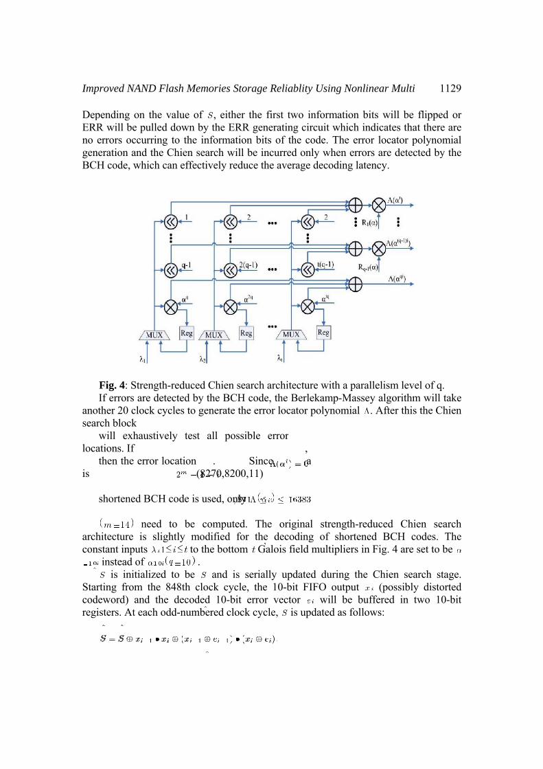
pending on R will be puerrors occureration and H code, whi
Fig. 4: StreIf errors arether 20 clocrch block will exhau
ations. If then the err
shortened B
nehitecture is stant inputs instead of
is initialrting from eword) andisters. At ea
ND Flash Me
the value oulled down rring to thethe Chien
ich can effe
ength-reducee detected bck cycles to
ustively tes
ror location
BCH code is
eed to be slightly m
s to
lized to be the 848th c
d the decodach odd-num
Memories Sto
of , either by the ERR
e informatiosearch will
ectively redu
ed Chien seby the BCH
generate th
st all possi
. (8270,8200
s used, only
computedmodified foro the bottom.
and is sclock cycleded 10-bit
mbered clock
orage Reliab
the first twR generatingon bits of th
be incurreduce the aver
arch architecode, the B
he error loca
ible error
Since 0,11)
y
. The origr the deco
m Galois fi
serially upde, the 10-bierror vectok cycle, is
blity Using
wo informatg circuit whhe code. Thd only whenrage decodin
ecture with aBerlekamp-Mator polynom
,a
ginal strengding of shield multipli
dated durinit FIFO outor will bs updated as
Nonlinear M
tion bits wihich indicatehe error locan errors are ng latency.
a parallelismMassey algomial . Afte
gth-reducedhortened BCiers in Fig. 4
ng the Chietput (pobe buffereds follows:
Multi 1
ill be flippees that thereator polynodetected by
m level of qorithm will er this the C
d Chien seCH codes. 4 are set to
en search stossibly distod in two 10
1129
ed or e are
omial y the
q. take
Chien
earch The be
tage. orted 0-bit
113
signmak
non
redunoninve(22)mulLet
real
0
Fi
At the 167nificant twoke adjustmeTheorem 3
nlinear 5-bit 1. All ope
perform2. The 5-d
serial dclock cywith a p
3. One mothe archblock an
The error muce the har
nlinear synderter in )]. In geneltipliers. Th
Given the flized using s
ig. 5: Decod
75 clock c bits are suc
ent to these t3 presentederror correcerations of
med in digit error cesign can acycles to theparallelism lore block fohitecture shnd generate
magnitude prdware ove
drome are is req
eral, invertehus a four-st
, can b
fact that a fosquare oper
der architectnonlinear 5
ycle, ccessfully ctwo bits accd in Sectiocting code af the decod
. correcting cchieve a sime decoder folevel of 10. or the comphown in Figes the final d
polynomial ierhead, mule reused to quired to coers in Galotage pipelinbe represent
our-stage pirations and
ture for the 5-error-corre
and are
corrected. Acording to thon V and are dif-feren der for the
code does nmilar de-codor the (828
putation of tg. 5. The bldecoded me
is generatedltipliers in generate th
ompute ois field hne is added ted as
ipeline is imfive multipl
E. Ramakr
proposed (8ecting code.
used to rA 2-bit errorhe check resthe decode
nt as followse 5-digit e
not require ding latency1,8201,11)
the error malock is connmory conte
d by the Be f
he error maaccording t
have much to reduce t
mplemented,lications in
rishna Naik
8281,8201,1.
recheck whr mask will sults. er for the s.
error cor-re
a par-allel y in terms o5-bit error
agni-tude isnected to thnts.
rlekamp-Mfor the calagnitude poto Forney’slonger cri
the latency
, the above .
& L.S. Dev
11)
hether the mbe generate
(8281,8201
cting code
architecturof the numbe
correcting c
s integrated he Chien se
assey blockculation of
oly-nomial. algorithm tical path of the inve
function caAgain we r
varaj
most ed to
1,11)
are
re. A er of code
into earch
k. To f the One [see than
erter.
an be reuse
Improved NAND Flash Memories Storage Reliablity Using Nonlinear Multi 1131
the multipliers in other blocks for the purpose of reducing the hardware overhead. Since the square operation is simple in , the inverter adds minimal area overhead and has a latency similar to the Galois filed multiplier in our design.
C. Area, Latency, and Power Consumption The area, latency, and the power consumption for architec-tures based on the six alternatives presented in Section V are shown in Table III. The designs are modelled in Verilog and synthesized in RTL Design Compiler using 45-nm NANGATE library [34]. In practice the logic circuits used in NAND flash memory could be different from those used in standard digital designs. The estimation presented here is only for the purpose of investigating the increase in area, power and latency of archi-tectures based on the proposed nonlinear multi-error correcting codes compared to architectures based on the widely used BCH codes and RS codes.
During the synthesis we fixed the clock rate for the encoder and the decoder and compared the area and the power consump-tion for architectures based on different codes. The encoders work at 1 GHz. The decoders work at a lower frequency— 400 MHz—due to the long critical path in Berlekamp-Massey block [12]. The six alternatives require the similar latency in terms of the number of clock cycles for encoding and decoding. Due to the computation of the error magnitude and the pipeline for the inverter in the Galois field, digit-error correcting codes (RS, etc.) need eight more clock cycles to complete the decoding compared to bit-error correcting codes (BCH, etc.).
The encoders for the digit-error correcting codes require 40% 50% more area overhead and power than the encoders for bit-error correcting codes (see Figs. 6 and 7) due to the fact that all operations are in . The decoders for digit-error correcting codes, however, require 20% 30% less overhead in area and power because of a much simpler serial architecture.
Compared to BCH codes and RS codes, the proposed non-linear multi-error correcting codes need about 10% 20% more area and power in total for the encoder and the decoder and have the similar latency in terms of the number of clock cycles required to complete the encoding and decoding. The(8281,8201,11) nonlinear 5-bit error correcting codes based on Theorem 3 (columns 6 and 7 in Table III), for example, requires 17.5% more area and consumes 10.0% more power in total for the encoder and the decoder compared to the (8262,8192,11) BCH code.
We note that the encoder and the decoder are only a very small portion in the MLC NAND flash memory chip, where the major portion is the memory cell array. Thereby the increase in area overhead for the encoder and the decoder is not significant for the reliable memory design.
5. Implementation and Results The proposed NAND Flash Memories Storage Reliablity Using Nonlinear Multi Error Correction Codes. The code is completely synthesized using Xilinx XST and
E. Ramakrishna Naik & L.S. Devaraj
1132
implemented on device family Spatran 3E, device XC3S500E, package FG 320 with speed grade -4.
6. Conclusion In this paper, the constructions of two nonlinear multi-error correcting codes are proposed. Their error correcting algorithms are presented. The proposed codes have much less undetectable and miscorrected errors than the conventional BCH codes and RS codes.
The designs of reliable MLC NAND flash memories based on the proposed nonlinear multi-error correcting codes are pre-sented. We compare the area, the latency and the power con-sumption of the reliable MLC NAND flash architectures using the proposed nonlinear multi-error correcting codes to architectures based on BCH codes and RS codes. The encoder and the decoder for all the alternatives are modeled in Verilog and synthesized in RTL Design Compiler. The results show that architectures based on nonlinear multi-error correcting codes can have close to zero undetectable and miscorrected errors while consuming less than 20% more area and power consumption than architec-tures based on the BCH codes and the RS codes.
References
[1] G. Atwood, A. Fazio, D. Mills, and B. Reaves, “Intel Strata memory technology overview,” Intel Technol. J., vol. 1, 1997 [Online]. Avail-able: http://www.intel.com/technology/itj/archive/1997.htm
[2] J. Cooke, “The inconvenient truths about NAND flash memory,” pre-sented at the Micron MEMCON Presentation, Santa Clara, CA, 2007.
[3] R. Dan and R. Singer, “Implementing MLC NAND flash for cost-effective, high capacity memory,” M-Syst. White paper, 2003 [Online]. Available: http://support.gateway.com/s/Manuals/Desk-
Improved NAND Flash Memories Storage Reliablity Using Nonlinear Multi 1133
[4] tops/5502664/Implementing_MLC_NAND_Flashwhite%20paper.pdf [5] R. Bez, E. Camerlenghi, A. Modelli, and A. Visconti, “Introduction to flash
memory,” Proc. IEEE, vol. 91, no. 4, pp. 489–502, Apr. 2003. [6] G. Cellere, S. Gerardin, M. Bagatin, A. Paccagnella, A. Visconti, Bonanomi,
S. Beltrami, R. Harboe-Sorensen, A. Virtanen, and [7] Roche, “Can atmospheric neutrons induce soft errors in NAND floating gate
memories?,” IEEE Electron Device Lett., vol. 30, no. 2, pp. 178–180, Feb. 2009.

E. Ramakrishna Naik & L.S. Devaraj
1134