Embed Size (px)
Citation preview

"Implementation Trade-offs of Triple-DES in the SRC Reconfigurable
Computing Environment"
Osman Devrim Fidanci 1, Hatim Diab 1, Tarek El-Ghazawi 1, Kris Gaj 2 and Nikitas Alexandridis 1
1: George Washington University2: George Mason University

Outline• Why Reconfigurable Computing ?
• SRC-6E General Purpose Reconfigurable Computer– Hardware Architecture– Programming Model
• Triple DES Encryption Algorithm– Single DES Algorithm– Triple DES with 2 Keys
• Implementation Trades-offs of Triple-DES in SRC
• ConclusionsFidanci D32

Why Reconfigurable Computing ?
Performance– Direct instantiation of hardware results in
better efficiency– Reduces I/O bandwidth requirements by
elimination of Load/Store paradigm
Scalability– Basic technology improving much faster than
Moore’s law– Takes advantage of parallelism found in many
programsFidanci D33

SRC-6E Hardware Architecture
L2
MIOCMIOC
L2
PCIPCISlotSlot
SSNNAAPP
PrivateMemory
µµP BoardP Board
XeonµP
L2
PCIPCISlotSlot
MIOCMIOC
PrivateMemory
SSNNAAPP
L2
µµP BoardP Board
Control ChipControl Chip
OnOn--Board Board MemoryMemory(24 MB)(24 MB)
(6x)(6x)
User User ChipChip
User User ChipChip
Control ChipControl Chip
OnOn--Board Board MemoryMemory(24 MB)(24 MB)
User User ChipChip
User User ChipChip
XeonµP
(6x)(6x)
(6x)(6x)
(6x)(6x)
XeonµP
XeonµP
MAP BoardMAP Board
Fidanci D34

SRC MAP Compiler Architecture
HLLHLLSourceSource
FORTRANFORTRAN&&CC
RC Compiling SystemRC Compiling System
MAPMAPMacrosMacros
CustomerCustomerMacrosMacros
RunRun--timetimeLibraryLibrary
ApplicationApplicationExecutableExecutableOptimization
Logic Partitioning
Synthesis Place & Route
Verilog Generation
DFG Generation
Fidanci D35
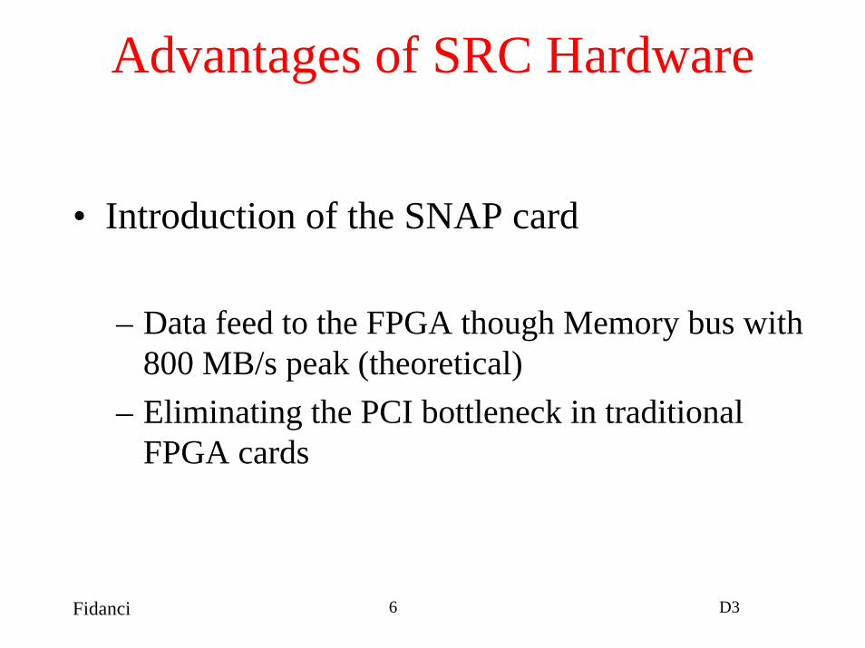
Advantages of SRC Hardware
• Introduction of the SNAP card
– Data feed to the FPGA though Memory bus with 800 MB/s peak (theoretical)
– Eliminating the PCI bottleneck in traditional FPGA cards
Fidanci D36

SRC-6E System SW
• System– Linux
• Red Hat 7.2• Driver and Library additions to support SNAP and MAP
• Compilers– Microprocessor and MAP
• Tools– WINE– FPGA
• Synplicity Synplify Pro• Xilinx Integrated Software Environment
Fidanci D37

Macro Development for SRC
• User macros can be defined in Verilog or VHDL• Three types of macros defined in SRC platform:
– Functional– Stateful– External
• System clock frequency is 100MHz. So, User macros should be optimized for this speed. Otherwise FIFO must be employed
Fidanci D38

General Depiction of DES Encryption Algorithm
Fidanci D39
64-bit inputs (plaintext and keys)
64-bit output (ciphertext)
16-round operation plus initial permutations
Pipelined, 17-clock cycles latency
Output generated at every clock cycle

Single Round of DES Algorithm
Expansion/permutation operation (E-table)
Logical XOR operations
Substitution/choice operation (S-box)
Permutation (P)
Fidanci D310

Triple DES with 2 KeysEncipher
Decipher
“Triple-DES with two keys” scheme is used for backward compatibility with DES (by setting two keys identical, provides single DES encryption/decryption).Triple DES requires 51-clock cycle to get ciphertext
Fidanci D311

Different Implementations of Triple DES in SRC
• Case 1Effect: DES macro is called three times from Fortran main file
• Case 2Effect: DES macro is called three times from Fortran subroutine file
• Case 3 Effect: Triple-DES macro is called once from Fortran main and subroutine files
Fidanci D312

Calling DES/Tri-DES macro from Fortran HLL
Main.f90
Subroutine1.mf
DES.v
Subroutine2.mf Subroutine3.mf
DES.v Tri-DES.v
3 times
3 times
Fidanci D313

Implied Architectures
Fidanci D314
DES
RAM
FPGA
3 times
17-clock cycles
RAM RAM
DES
DES
DES
TripleDES
FPGA FPGA
51-clock cycles51-clock cycles
Case 1 Case 2 Case 3

Processing Time Measurement
• The timer macro is simply a counter running at 100 MHz
• There are two calls: - start_timer: zeros out the counter- read_timer: gets the counter’s current value
Fidanci D315

Implementation Trades-Offs of Triple DES in SRC
Experiment(1) Experiment(2) Experiment(3)
Maximum Clock Speed(MHz)
102.3 100.8 101.8
CLB Slices (Tot. equiv. Gate
count)
6,177(163,835)
13,269(382,927)
11,786 (359,635)
Total Processing Time (91 blocks
of data)(ns)
4440 1820 1820
Fidanci D316

Timing Estimations
Total execution time =
Transfer time + Total processing timeµP memory ↔ on-board memory
Measuredexperimentally
Fidanci D317

Timing Estimations – cont.
Total processing time =
Load time + #pipeline_stages + (N-1) + Store timefirst block last block
x t
N – number of data blocks being processedt – number of subroutine calls
Load time + Store time = Load/Store time = TLS (unknown)
where
Fidanci D318

Timing Estimations – cont.
Case 1 Case 2 Case 3
#_pipeline stages: 17#_data blocks = N: 91#_subroutine_calls = t: 3Load/Store time: TLS
Clock period: 10ns
Estimated # of clock cycles for processing 91 blocks:[(17 + 90) + TLS] x 3 = 444
Load/Store time: TLS = 41
#_pipeline stages: 51#_data blocks = N: 91#_subroutine_calls = t: 1Load/Store time: TLS
Clock period: 10ns
Estimated # of clock cycles for processing 91 blocks:[(51 + 90) + TLS] = 182
Load/Store time: TLS = 41
#_pipeline stages: 51#_data blocks = N: 91#_subroutine_calls = t: 1Load/Store time: TLS
Clock period: 10ns
Estimated # of clock cycles for processing 91 blocks:[(51 + 90) + TLS] = 182
Load/Store time: TLS = 41
Fidanci D319

I/O Overhead (TLS/Total time)
Case 1 Case 2 Case 3
91 data blocks 27.7 % 22.5 % 22.5 %
501 data blocks 7.3 % 6.9 % 6.9 %
1001 data blocks 3.8 % 3.7 % 3.7 %
10001 data blocks 0.4 % 0.4 % 0.4 %
Fidanci D320

Ratio of processing timesCase 1 Total processing timeCase 2&3 Total processing time =
(17 + (N-1) + 41) x 3==
(51 + (N-1) + 41)
Fidanci D321
N 91 501 1,001 10,001
2.99ratio 2.44 2.83 2.91

Discussion
Case 2, i.e., calling DES macro three times fromthe Fortran subroutine, and
Case 3, i.e., calling 3DES macro once from the Fortran subroutine
almost equivalent– the same execution time– area 13% larger for Case 2 because of the default
interface between single DES modules
Fidanci D322

Discussion – cont.
Case 1, i.e., calling DES macro three times fromthe Fortran main file, and
Cases 2 and 3very different
– approximately two times smaller area for Case 1– over two times longer execution time caused by the
larger number of iterations, larger I/O overhead (communication between FPGA and on-board memory) and smaller utilization of the pipeline
Fidanci D323

Conclusions
• SRC Programming Model enables flexible choice of the hardware architecture used to implement required function
• Implied architecture depends on – function (granularity) of the hardware description
language macro– placement of macro calls in a high level language
program
Fidanci D324

Conclusions – cont.
• Common features of all implemented architectures– deep pipelining– operational clock frequency 100 MHz
• Overhead associated with the run-time communication between FPGA (User Chip) and on-board memory can be made negligible for processing of large amounts of data
Fidanci D325