Embed Size (px)
Citation preview
International Journal of Computer and Electrical Engineering, Vol. 1, No. 4, October, 2009 1793-8163
- 443 -
Abstract—Among the various power quality problems, the
voltage sags, are attracting a large amount of attention of researchers from industry. Dynamic Voltage Restorer(DVR) gives the solution to the above mentioned problem. The main function of DVR is to mitigate the voltage sag. It controls voltage applied to the load by injecting voltage of compensating amplitude, frequency and phase angle to the distribution line. The DVR is primarily responsible for restoring the quality of voltage delivered to the end user when the voltage from the source is not appropriate to be used for sensitive loads. Usage of DVR enables consumers to isolate and protect themselves from transients and disturbances caused- by sags. DVR is simulated using Matlab and it is implemented using microcontroller 89C2051. The experimental results are compared with the simulation results Index Terms— DVR, Matlab, Microcontroller 89C2051
I. INTRODUCTION With the rapid technology advancements in industrial
control processes, electric utilities are experiencing more demanding requirements on the power quality from the large industrial power consumers. Such power quality problems have been better appreciated when the price paid due to the economic losses caused by them is large. These concerns are reflected in the newer versions of power quality standards, such as IEEE 1159-1995 [1] and IEC6100-4-30 [2]. Trends of deregulation happening in Europe and America exert pressures on the utilities to accommodate such demanding requirements in a competitive electricity market environment.
Among the various power quality problems, the voltage sag, usually resulting from the faults on parallel transmission/distribution feeders, is attracting quite a large amount of attention of researchers from both industry and academia [3]-[5]. A definitive solution to this problem at large power levels has been commonly called dynamic voltage restorer (DVR), under the rubric of the custom power concept introduced by EPRI [6]. The main function of DVR is to mitigate the voltage sag, although sometimes, additional functions such as harmonic compensation and reactive power
Manuscript received April 29, 2009. N. S. Sakthivel Murugan is research scholar of Anna University, Chennai.
(Phone: +914285 228361; Mobile: +90 9003555134). Dr. A. Nirmalkumar was with N. S. S. College of Engineering, Palakkad,
Kerala, India. He is now with Bannari Amman Institute of Technology, Sathyamangalam, 638476 Erode(Dt.), Tamilnadu, India.
T. Vijayakumar was with Kumaraguru College of Technology, Coimbatore and is now with Karpagam college of Engineering, Coimbatore, Tamilnadu. India.
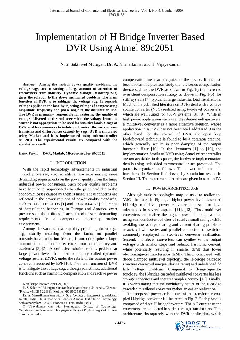
compensation are also integrated to the device. It has also been shown in a previous study that the series compensation device such as the DVR as shown in Fig. 1(a) is preferred over shunt compensation strategy as shown in Fig. 1(b) for stiff systems [7], typical of large industrial load installations. Much of the published literature on DVRs deal with a voltage source converter (VSC) realized using two-level converters, which are well suited for 480-V systems [8], [9]. While in high power applications such as at distribution voltage levels, a multilevel converter is a more attractive solution, whose application in a DVR has not been well addressed. On the other hand, for the control of DVR, the open loop feed-forward technique is found to be a common practice, which generally results in poor damping of the output harmonic filter [10]. In the literatures [1] to [10], the implementation details of DVR using Atmel microcontroller are not available. In this paper, the hardware implementation details using embedded microcontroller are presented. The paper is organized as follows. The power architecture is introduced in Section II followed by simulation results in Section III. The experimental results are given in section IV.
II. POWER ARCHITECTURE Although various topologies may be used to realize the
VSC illustrated in Fig. 1, at higher power levels cascaded H-bridge multilevel power conveners are seen to have advantages in several aspects [11], [12]. First, multilevel converters can realize the higher power and high voltage using semiconductor switches of relative small ratings while avoiding the voltage sharing and current sharing problems associated with series and parallel connection of switches commonly employed in two-level converter realization. Second, multilevel converters can synthesize the output voltage with smaller steps and reduced harmonic content, while potentially resulting in smaller dv/dt thus lower electromagnetic interference (EMI). Third, compared with diode clamped multilevel topology, the H-bridge cascaded structure can avoid unequal device rating and unbalanced dc link voltage problems. Compared to flying-capacitor topology, the H-bridge cascaded multilevel converter has less storage capacitors and requires simpler control [13]. Finally, it is worth noting that the modularity nature of the H-bridge cascaded multilevel converter makes an easier realization.
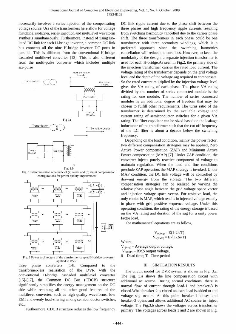
The proposed power architecture of the transformer cou-pled H-bridge converter is illustrated in Fig. 2. Each phase is composed of three H-bridge inverters. The AC outputs of the converters are connected in series through transformers. This architecture fits squarely with the DVR application, which
Implementation of H Bridge Inverter Based DVR Using Atmel 89c2051
N. S. Sakthivel Murugan, Dr. A. Nirmalkumar and T. Vijayakumar
International Journal of Computer and Electrical Engineering, Vol. 1, No. 4, October 2009 1793-8163
- 444 -
necessarily involves a series injection of the compensating voltage source. Use of the transformers here allow for voltage matching, isolation, series injection and multilevel waveform synthesis simultaneously. Furthermore, instead of using iso-lated DC link for each H-bridge inverter, a common DC link bus connects all the nine H-bridge inverter DC ports in parallel. This is different from the conventional H-bridge cascaded multilevel converter [13]. This is also different from the multi-pulse converter which includes multiple six-pulse
Fig 1a
Fig. 1.b
Fig. 1 Interconnection schematic of (a) series and (b) shunt compensation configurations for power quality improvement
Fig. 2 Power architecture of the transformer coupled H-bridge converter
applied to DVR. three phase converters [14]. Compared to the transformer-less realisation of the DVR with the conventional H-bridge cascaded multilevel converter [15]-[17], the Common DC Bus (CDCB) structure significantly simplifies the energy management on the DC side while retaining all the other good features of the multilevel converter, such as high quality waveforms, low EMI and evenly load-sharing among semiconductor switches, etc..
Furthermore, CDCB structure reduces the low frequency
DC link ripple current due to the phase shift between the three phases and high frequency ripple currents resulting from switching harmonics cancelled due to the carrier phase shift. The three transformers in each phase could be one transformer with three secondary windings, which is a preferred approach since the switching harmonics cancellation will reduce the core loss. However, to keep the modularity of the design, a separate injection transformer is used for each H-bridge.As seen in Fig.2, the primary side of the injection transformer carries the rated load current. The voltage rating of the transformer depends on the grid voltage level and the depth of the voltage sag required to compensate. So the rated current multiplied by the injection voltage level gives the VA rating of each phase. The phase VA rating divided by the number of series connected module is the rating for one module. The number of series connected modules is an additional degree of freedom that may be chosen to fulfill other requirements. The turns ratio of the transformer is determined by the available voltage and current rating of semiconductor switches for a given VA rating. The filter capacitor can be sized based on the leakage inductance of the transformer such that the cut off frequency of the LC filter is about a decade below the switching frequency.
Depending on the load condition, mainly the power factor, two different compensation strategies may be applied, Zero Active Power compensation (ZAP) and Minimum Active Power compensation (MAP) [7]. Under ZAP condition, the converter injects purely reactive component of voltage to maintain regulation. When the load and line conditions preclude ZAP operation, the MAP strategy is invoked. Under MAP condition, the DC link voltage will be controlled by drawing energy from the storage. The two different compensation strategies can be realized by varying the relative phase angle between the grid voltage space vector and injection voltage space vector. For resistive load, the only choice is MAP, which results in injected voltage exactly in phase with grid positive sequence voltage. Under this operating condition, the rating of the energy storage is based on the VA rating and duration of the sag for a unity power factor load.
The mathematical equations are as follow,
Vo(Avg) = E(1-2δ/T) Vo(RMS) = E√(1-2δ/T)
Where, Vo(Avg) – Average output voltage, Vo(RMS) – RMS output voltage, δ – Dead time; T– Time period
III. .SIMULATION RESULTS The circuit model for DVR system is shown in Fig. 3.a.
The Fig. 3.a shows the line compensation circuit with additional ac source. During normal conditions, there is normal flow of current through load-1 and breaker-3 is closed.When breaker-2 is closed an extra load is added to and voltage sag occurs. At this point breaker-1 closes and breaker-3 opens and allows additional AC source to inject voltage. The Fig.3.b shows the voltages across transformer primary. The voltages across loads 1 and 2 are shown in Fig.
International Journal of Computer and Electrical Engineering, Vol. 1, No. 4, October 2009 1793-8163
- 445 -
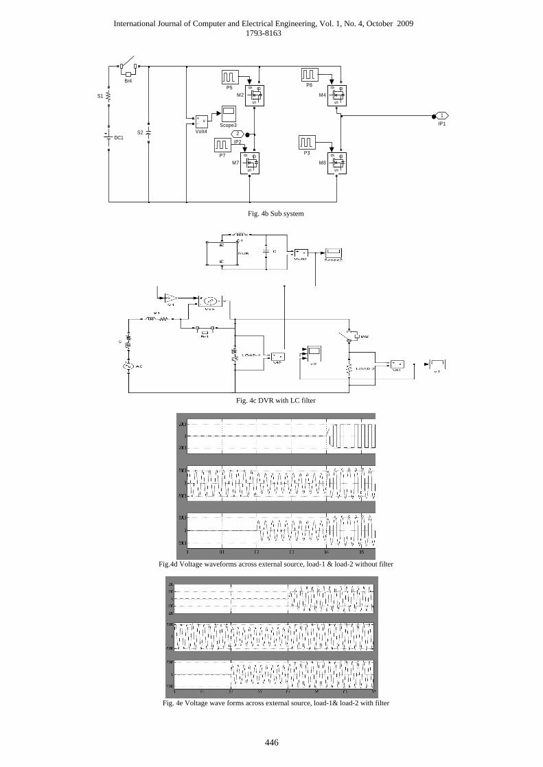
3c. The Fig.4.a shows the line compensation with DVR circuit. The DVR model is shown in Fig. 4.b. The DVR system has four MOSFETs. The driving pulses are produced by AT89C2051 microcontroller. The LC filter is added with DVR to get better output. The Fig. 4c shows the DVR circuit
with LC filter. The Fig.4d and Fig. 4e show the voltage across external source and compensated voltage across load-1 and load-2 without and with filter respectively. From this figure it can be seen that proper voltage is injected to improve the voltage profile.
e3
e2e1
v+-
Vt5
v+-
Vt2 v+-
Vt1
S1
S
12
Li
LOAD-2
LOAD-1
Br3 Br2
Br1AC2
AC
Fig.3a. Line compensation circuit with additional AC source
Fig. 3b Voltage across transformer primary
Fig. 3c Voltage across load -1 and load-2
Fig. 4a Line compensation circuit with DVR circuit
International Journal of Computer and Electrical Engineering, Vol. 1, No. 4, October 2009 1793-8163
446
2IP2
1IP1v+
-
Volt4Scope3
S2
S1
P8
P7
P5
P3 g DS
M8
g DS
M7
g DS
M4
g DS
M2
DC1
Br4
Fig. 4b Sub system
Fig. 4c DVR with LC filter
Fig.4d Voltage waveforms across external source, load-1 & load-2 without filter
Fig. 4e Voltage wave forms across external source, load-1& load-2 with filter
International Journal of Computer and Electrical Engineering, Vol. 1, No. 4, October 2009 1793-8163
- 447 -
U3
IR2110
1710
11
12
13
26395
LOHOHIN
SHDN
LIN
VSS
COMVBVCCVDDVS
47E-6
D1
1N450012
U2
L7805/TO220
1 2VIN VOUT
22E
12
22E
Y1
ZTB
M3
R10
1k
100E
M1
D2
1N450012
12
D4
1N450012
0
U1
L7812/TO3
1 2VIN VOUT
D5
1N450012
22E
SW1
SW PUSHBUTTON
47E-6
0
M2
22E
R1
1k
U5
IR2110
1710
11
12
13
26395
LOHOHIN
SHDN
LIN
VSS
COMVBVCCVDDVS
V1
FREQ = 50HZ
VAMPL = 230V
100E
C5
33E-12
47E-6
C7
33E-12
47E-6
U4
AT89C2051
1
20
54
1213141516171819
23678911
RST/VPP
VCC
XTAL1XTAL2
P1.0/AIN0P1.1/AIN1P1.2P1.3P1.4P1.5P1.6P1.7
P3.0/RXDP3.1/TXD
P3.2/INT0P3.3/INT1
P3.4/T0P3.5/T1
P3.7
12V
M4
D3
LED
C1
1000E-6
C10
10E-6
5V
TX1
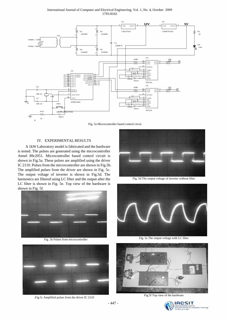
Fig. 5a Microcontroller based control circui
IV. EXPERIMENTAL RESULTS A 1kW Laboratory model is fabricated and the hardware
is tested. The pulses are generated using the microcontroller Atmel 89c2051. Microcontroller based control circuit is shown in Fig.5a. These pulses are amplified using the driver IC 2110. Pulses from the microcontroller are shown in Fig.5b. The amplified pulses from the driver are shown in Fig. 5c. The output voltage of inverter is shown in Fig.5d. The harmonics are filtered using LC filter and the output after the LC filter is shown in Fig. 5e. Top view of the hardware is shown in Fig. 5f.
Fig. 5b Pulses from microcontroller
.Fig.5c Amplified pulses from the driver IC 2110
Fig. 5d The output voltage of inverter without filter
Fig. 5e The output voltage with LC filter
Fig.5f Top view of the hardware
International Journal of Computer and Electrical Engineering, Vol. 1, No. 4, October 2009 1793-8163
- 448 -
V. CONCLUSION The Dynamic Voltage Restorer (DVR) is used to improve
voltage sags caused by abrupt increase in loads. The DVR reduces losses associated with irregularities in the production process resulting from power disturbances. DVRs tackle the problem of harmonics caused by non-linear load machinery in manufacturing facilities. The insulation wear on transformers, motors and drivers caused by power irregularities is also reduced by DVR. Therefore most industries use DVR which compensates voltage sag especially at sensitive loads by injecting an appropriate voltage through an injection transformer. The hardware is implemented using an embedded microcontroller and the results are presented. The experimental results closely agree with the simulation results.
REFERENCES [1] IEEE Recommended Practice for Monitoring Electric Power Quality,
IEEE Std, 1159-1995, 1995. [2] Testing and Measurement Techniques – Power Quality Measurement
Methods, IEC 61000-4-30, 2003. [3] J.G.Nielsen, M.Newman, H.Nielsen aned F.Blaabjerg, “control and
testing of a dynamic voltage restorer (DVR) at medium voltage level,” IEEE Trans. Power Electron., vol.19,no. 3, p. 806, May 2004.
[4] N.H. Woodley, “Field experience with dynamic voltage restorer (DVRTMMV) systems,” in Proc. IEEE Power Eng, Soc. Winter Meeting. Conf., Singapore, 2000, P. 2864.
[5] N.H. Woodley, L.Morgan, and A.Sundaram, “Experience with an inverter-based dynamic voltage restorer,” IEEE Trans. Power Delivery, vol. 14, no. 3, p. 1181, Aug, 1999.
[6] N.G.Hingorani, “Introducing custom power,” IEEE Spectrum, vol. 32, no.6, p.41, 1995.
[7] B.Wang and G.Venkataramanan, “Evaluation of shunt and series power conditioning strategies for feeding sensitive loads,” in Proc. 127th Annu. IEEE Appl. Power Electron. Conf., Anaheim, CA, 2004, pp. 1445-51
[8] Z.Changjiang, A.Arulampalam, and N.Jenkins, “Four-wire dynamic voltage restorer based on a three-dimensional voltage space vector PWM algorithm,” IEEE Trans. Power Electron., vol. 18, no. 4, p. 1093, July 2003
[9] W.E.Brumsickle, R.S.Schneider, G.A.Luckjiff, D.M.Divan, and M.F.McFranaghan, “Dynamic sag correctors: Cost-effective industrial power line conditioning,” IEEE Trans. Ind. Appl., vol.37, no. 1,p.212, Jan./Feb.2001
[10] M.Vilathgamuwa, A.A.D.R.Perera, and S.S.Choi, “Performance improvement of the dynamic voltage restorer with closed-loop load voltage and current-mode control,” IEEE Trans. Power Electron., vol. 17, no. 5, p.824, Sep.2002
[11] L.M.Tolbert, P.F.Zheng,and T.G.Habetler, “Multilevel converters for large electric drives,” IEEE Trans. Ind. Appl., vol.35, no. 1,p.36,Jan/Feb. 1999
[12] R.Kieferndorf, G.Venkataramanan, and M.D.Manjrekar, “Power electronic transformer (PET) fed nine-level H-bridge inverter for large induction motor drives,” in Proc. IAS Annu. Meeting, Rome, Italy, 2000. pp. 2489-2495
[13] J.S.Lai and F.Z.Peng, “Multilevel converters- A new breed of power converters,” IEEE Trans. Ind. Appl., vol. 32, no. 3, pp. 509-517, May/ Jun. 1996
[14] S.Mori, K.Matsuno, T.Hasegawa, S.Ohnishi, M.Takeda, M.Seto, S.Murakami, and F.Lshiguro, “Development of a large static VAR generator using self-commutated inverters for improving power system stability,” IEEE Trans. Power Syst., vol. 8, no. 1,pp. 371-377,feb. 1993.
[15] B.H.Li, S.S.Choi, and D.M.Vilathgamuwa, “Transformerless dynamic voltage restorer,” IEEE Power Electron. Lett., vol. 2, no. 4, pp. 125-130, Apr.2002.
[16] P.C.Loh, D.M.Vilathgamuwa, S.K.Tang, and H.L.Long, “Multilevel dynamic voltage restorer,” IEEE Power Electron. Lett., vol. 2 , no.4, pp. 125-130, Apr. 2004.
[17] A.J.Visser, J.H.R.Enslin, and H.D.T.Mouton, “Transformerless series sag compensation with a cascaded multilevel inverter,” IEEE Trans. Ind. Electron., vol.49, no.4, pp. 824-831, Aug.2002.
[18] Y.Fukuta and G.Venkataramanan, “DC bus ripple minimization in cascaded H-bridge multilevel converters under staircase modulation,” in Proc. IAS Annu. Meeting, Pittsburgh, PA, 2002, p. 1988.
[19] G.Venkataramanan and B.Wang, “Dynamic modeling and control of three phase pulse width modulated power converters using Phasors,” in Proc. IEEE 35th Power Electron. Spec. Con., Aachen, Germany,
About authors
N.S.Sakthivel Murugan has obtained his B.E. degree from Madras University and M.E. Degree from Annamalai University in the year 1998 and 2001 respectively. He has 11 years of teaching experience. He is presently a research scholar at Anna University. His research area is improvement
of power quality using DVR. He is a life member of ISTE.
Dr.Nirmalkumar has obtained his U.G. degree from Calicut University and P.G. Degree from Kerala University in the year 1972 and 1976 respectively. He has done his research from Bharathiyar University. He has 28 years of teaching experience. He is presently working as Prof. and Head of EEE department at BIT, Sathyamangalam. His
research area is power quality issues in power systems.
T.Vijayakumar has obtained his B.E. Degree from Bharathiar University and M.E. degree from Annamalai University in the year 1998 and 2001 respectively. He has 11 years of teaching experience. His research area is reactive power compensation in electrical power systems.