Embed Size (px)
Citation preview

IMPLEMENTATION OF A SOFTWARE DEFINED RADIO ON FPGAs
USING SYSTEM GENERATOR
A Thesis Presented for the
Master of Science Degree The University of Tennessee at Chattanooga
Tanvika M. Patel May 10, 2010

ii
Certification of Final Defense of Thesis
The Graduate School The University of Tennessee at Chattanooga
This is to certify that
Tanvika Patel Zgv565
A candidate for the Master of Science in Electrical Engineering
Passed
The defense of
IMPLEMENTATION OF A SOFTWARE DEFINED RADIO ON FPGAs USING
SYSTEM GENERATOR
05/10/2010
Committee Names and Signatures Name (Chairperson) Signature
Name (Committee Member) Signature
Name (Committee Member) Signature

i
ABSTRACT
The aim of this thesis is to implement a Software Defined Radio based wireless
communication system using a Xilinx Spartan 3E Field Programmable Gate Array.
Software Defined Radio refers to the class of reprogrammable radios in which the same
piece of hardware can perform different functions at different times. Xilinx’s System
Generator for Digital Signal Processor tool is used to simulate and implement AM
modulation on the Spartan 3E Starter Board.
This paper includes detailed procedure to create a radio design using Matlab
Simulink and download the design onto the Spartan 3E board has been documented. The
performance of a baseband radio transmitter is analyzed using waveforms for three
different modulation techniques. The Modulation techniques include Amplitude
Modulation, Amplitude Shift keying and Binary phase shift keying. The radio
performance in real time is also analyzed by implementing these modulation techniques
on the hardware using a Xilinx Spartan 3E board. By comparing the waveforms
generated by implementing on the hardware and waveforms obtained by the Simulink,
the system was validated.

ii
ACKNOWLEDGEMENTS
I would like to express my appreciation to my thesis advisor Dr. Stephen Craven
for his support and guidance. He has been constant source of inspiration and has provided
consistent support and valuable suggestion throughout this project without which this
work wouldn’t have been possible.
I would also like to thank Dr. Ahmed Eltom and Dr. Clifford Parten for their
interest in the project and for being a part of my committee. I would also like to thank
the Department of Electrical Engineering at University of Tennessee at Chattanooga for
giving me the opportunity to do Master’s degree in this honorable institution.
I would like to express my heart-felt gratitude to my family for their
encouragement and support without which I wouldn’t have come so far. Finally I would
like to thank all my friends for their invaluable support and cooperation.

iii
LIST OF TABLES TABLE PAGE 1.1 Difference between Conventional Radio and Software Defined Radio 4

iv
LIST OF FIGURES FIGURE PAGE 1.1 (a) Block diagram of Conventional Radio………………………………………….4
1.1 (b) Block Diagram of SDR…………………………………………………………4
2.1 Basic block diagram of SDR System……………………………………………8
2.2 USRP Hardware and Block diagram…………………………………………..12
2.3 Basic Architecture of GNU radio.......................................................................13
3.1 Functional block diagram of digital transceiver …………………...………….15
3.2 Demonstrating DDC On the Signal Lying In the Range of 39-40 MHz………17
3.3 Design flow using Xilinx system generator…………………………….……...19
3.4 Demonstrating DDC On the Signal Lying In the Range Of 39-40 MHz……...21
3.5 System Generator dialog box…...………………...............................................22
4.1 Radio Set Up…………………………………………..……………………….26
4.2 Simulation Model For AM Modulation………….………………………….....28
4.3 (a) Modulating Signal……………………………………………………………..29
4.3 (b) Carrier Signal……………………………………………...…………………..29
4.3 (c) Modulated Signal in Simulink………….………………….…………………..29
4.4 Modulated Waveform Viewed with Oscilloscope…………………….……..30
4.5 Basic block Diagram of ASK…………………………………………….........31
4.6 (a) ASK Modulated Signal……………………………………………………….. 32
4.6 (b) OOK Modulated Signal in Simulink…………………………….…………….32
4.7 OOK Modulated waveform viewed with Oscilloscope……...…………………33
4.8 Basic Block Diagram of BPSK Modulator……………………………………..34

v
4.9 (a) BPSK Waveform in Simulink………………………………………………….35
4.9 (b) BPSK Modulated Waveform Viewed with Oscilloscope…..………………….

vi
LIST OF ACRONYMS
ADC Analog to Digital Converter
AM Amplitude Modulation
ASK Amplitude Shift Keying
AGC Automatic Gain Control
ASIC Application Specific Integrated Circuit
BPSK Binary Phase Shift Keying
BPF Band Pass Filter
CDMA Code Division Multiple Access
DDS Direct Digital Synthesizer
DAC Digital to Analog Converter
DSP Digital Signal Processor
DDC Digital Down Converter
DSB Double Side Band
DUC Digital Up Conversion.
FCC Federal Communication Commission
FPGA Field Programmable Gate Array
FM Frequency Modulation
FIR Finite Impulse Response
FFT Fast Fourier Transform
GUI Graphical User Interface
GPP General Purpose Processors
HDL Hardware Description Language

vii
HR Hardware Radio
ISDR Ideal Software Defined Radio
IF Intermediate Frequency
ISE Integrated Software Environment
KHz Kilo Hertz
LO Local Oscillator
LUT Look Up Table
MHz Mega Hertz
MIMO Multiple Input Multiple Output
OOK On- Off Keying
PC Personal Computer
PMOD Peripheral Modules
RF Radio Frequency
RSSI Received Signal Strength Indication
RAM Random Access Memory
SDR Software Defined Radio
SCR Software Controlled Radio
TDMA Time Division Multiple Access
USRP Universal software radio peripheral
USB Universal Serial Bus
VHSIC Very High Speed Integrated Circuit
VHDL VHSIC Hardware Description Language
XST Xilinx Synthesis Tool

viii
TABLE OF CONTENTS
CHAPTER PAGE
I. ABSTRACT …………………………………………………………………………. i
II. ACKNOWLEDGEMENT…………………………………………………………… ii
III. LIST OF TABLE……………………………………………………………………. iii
IV. LIST OF FIGURE………………………………………………………………….. .iv
V. LIST OF ACRONYMS…………………………………………………………….... v
1.INTRODUCTION …………………………………………………………………….. 1
1.1 Introduction…………………………………………………………………. 1
1.2 Software Defined Radio versus Conventional Radio……………………….. 3
1.3 Outline of Thesis ………………………………………………………….......5
2.BACKGROUND………………………………………………………………………. 6
2.1 Introduction…………………………………………………………………. 6
2.2 Definitions of Software Defined Radio……………………………………....7
2.3 Characteristics of Software Defined Radio…………………………………..8
2.4 Advantages and Disadvantages of Software Defined Radio………………...9
2.5 Implementation Platform…………………………………………………….10
2.6 USRP………………………………………………………………………...11
2.7 GNU Radio…………………………………………………………………..12
2.8 System Generator…………………………………………………………….13
3. SDR DESIGN METHODOLOGY……………………………………………………15
3.1 Wireless Communication System Model for Software Defined Radio 15

ix
3.1.1 DDC and DUC……………………………………………………..15
3.1.2 Basic Transceiver Function………………………………………..17
3.2 System Generator Design Flow………...……………………………………18
3.3 Simulation with System Generator and Simulink…………………………....20
3.4 Bitstream Generation …………………..…………………………………....22
4. EXPERIMENTAL SET UP, SIMULATIONS AND RESULTS……………………24
4.1 Introduction…………………………………………………………………..24
4.2 Basic Modulation Concept……………………………………………………24
4.3 Amplitude Modulation (AM)…………………………………………………24
4.3.1 AM SDR Setup……………...………………………………………..25
4.3.2 System Generator Implementation…………………………………....26
4.4 Amplitude Shift Keying………………………………………………………..30
4.5 Binary phase shift keying (BPSK)……………………………………………..33
5. CONCLUSION AND FUTURE WORK ……………………………………………35
5.1 Conclusion…………………………………………………………………….35
5.2 Suggestion for future work…………………………………………………... 36
REFERENCES…………………………………………………………………………37

1
CHAPTER 1
Introduction
1.1 Introduction
Wireless communication networks have become more popular in the past two
decades since the advent of cellular communications. Today advancements in wireless
technology and wireless applications require flexibility in the hardware. It is very
expensive and time consuming to create new radios in response to changing wireless
standards and applications [1]. Software radio can offer solutions to these problems by
moving analog circuit components into the digital domain. Programmable logic devices,
such as Field Programmable Gate Arrays (FPGAs) can be used to implement the radio
functions.
Software Defined Radio (SDR) has gained much interest in recent years due to
the advancements in processor and FPGA technology. FPGAs provide the capability of
cheaply implementing functionality that previously was created using analog hardware
components. FPGAs are built from one basic reconfigurable logic cell duplicated
thousands of times. A logic cell is basically a small lookup table (LUT), a D flip-flop and
a 2-to-1 multiplexer. The LUT is like a small RAM that can implement any logic function
up to four inputs. Complex logic functions are created by connecting number of logic
cells together through interconnect resources (wires and multiplexer placed around logic
cell). Designs targeting FPGAs are typically described using Hardware Descriptions
Languages (HDLs). However, in this thesis digital functional blocks that needed to be
programmed in the FPGA core are designed and simulated using MATLAB and add-on
programs.

2
“In a Software Defined Radio (SDR), functions that were formerly carried out
solely in hardware, such as the generation of the transmitted signal and the tuning and
detection of the received radio signal, are performed by software that controls high speed
signal processors [6]”.
Reconfigurability in radio technology in radio development is not a new technique.
In the 1980s, the first reconfigurable receiver was developed for radio intelligence to
intercept and record enemy radio transmission and to determine their locations in the
short wave range [1]. As per SDR forum discussion the difference between different
levels of flexibility in a radio are as follows:
1) Hardware Radio (HR): Hardware Radio is defined as radio in which there is no
software control of the hardware. The function of the hardware is set so it cannot be
changed [13].
2) Software Controlled Radio (SCR): In this radio only the control functions are
implemented in software. For example, the transmitter parameters like the
transmitted power level are controlled by software, while the other functions are
fixed in hardware [6].
3) Software Defined Radio (SDR): The name itself suggests that all radio functions are
implemented by software. These functions include modulation, multiplexing,
amplification, mixing, multiple access and other transmitter and receiver processes
[6].
4) Ideal Software Defined Radio (ISDR): ISDR is same as SDR except that it does not
include front end analog. Ideal SDR is one that has a transceiver that performs up
conversion and down conversion between baseband and the Radio Frequency (RF)

3
carrier exclusively in the digital domain, reducing the RF interface to a power
amplifier in the transmit path, a low noise amplifier in the receive path, and little or
no analog filtering. ISDR is currently unachievable due to the lack of very high
frequency RF-to-Digital converters capable of converting carrier frequencies
directly to digital data [6].
1.2 Software Defined Radio versus Conventional Radio
Figure 1.1(a) shows the basic block diagram of a conventional radio. In a
conventional radio’s receive path, the radio RF signal is received by an antenna and it
goes through a band pass filter. Frequency conversion from the transmitted RF to a lower,
intermediate frequency (IF) is accomplished by multiplying the RF signal by a sinusoidal
local oscillator (LO) in the mixer. An Analog to Digital Converter (ADC) then samples
the output from the final IF stage and the digital data are processed by a Digital Signal
Processing (DSP) circuit. The components from antenna to ADC are all analog circuits. If
more stages of down conversion exist, then more analog components are needed. Analog
components have limitations on signal processing capabilities and flexibility. And also
analog components are expensive. If the number of analog components is reduced, it will
result in simplification of the radio system, which in turn will result in higher reliability
and reduced cost. It would be best if all the intermediate analog stages could be replaced
by digital components, so that the antenna is directly connected to an ADC or DAC. This
is shown clearly in Figure 1.1(b). The idea behind software defined radio is to move as
much of the radio functionality as possible into software. For low frequency SDR, all the
RF tasks (DUC,DDC) can be performed on the FPGA, allowing the ADC to sample the
antenna directly.

4
(a)
(b)
Figure 1.1 (a) Block Diagram of Conventional Radio (b) Block Diagram of SDR
Air interface is the technology used for the radio transmission between base
station and mobile units in a wireless network, such as, Time Division Multiple Access
(TDMA) and Code Division Multiple Access (CDMA). To compare the functionalities of
conventional radio and SDR, A tabulation of their functions is provided in Table 1.1.

5
Table 1.1 Difference between Conventional Radio and Software Defined Radio [19].
Conventional Radio Software Defined Radio
Radio functionalities are primarily defined in hardware with minimum configurability in software.
Radio functionalities are defined in software.
Upgrading of design is not possible. Upgrading is easy because of software based architecture.
User has to use different mobile devices because of incapability of standards.
Global mobility can be achieved by downloading the appropriate air interface (TDMA, CDMA) thus overcoming the incapability of standards.
Less efficient Reprogrammability makes SDR more efficient and compact
1.3 Outline of Thesis
In this thesis Chapter 2 presents the background of software defined radio. This
presents the fundamentals of software defined radio, general background information and
various definitions of the software defined radio. It also presents the existing technologies
in the SDR field. Chapter 3 presents a design methodology for implementation on FPGAs
using the Xilinx System Generator software. Chapter 4 presents the experimental set up.
Simulation results for the different modulation techniques such as AM modulation,
Amplitude Shift Keying (ASK), On-Off Keying (OOK), Binary Phase Shift Keying
(BPSK) modulation are analyzed. AM modulation is implemented on the Xilinx Spartan
3E Starter Kit. Chapter 5 summarizes the Thesis content and also discusses future work.

6
CHAPTER 2.
BACKGROUND
2.1 Introduction
In traditional architectures all modulation and demodulation is performed in the
analog domain. Over the last few years, analog radio systems are being replaced by
digital radio systems for various radio applications in military, civilian and commercial
spaces. In addition to this, programmable hardware modules are increasingly being used
in digital radio systems at different functional levels. SDR technology aims to take
advantage of these programmable hardware modules to build open architecture based
radio system software [12].
Traditional hardware based radio devices limit cross functionality and can only be
modified through physical intervention. This results in higher production costs and
minimal flexibility in supporting multiple waveform standards. Software Defined Radio
technology provides an efficient and comparatively inexpensive solution to this problem,
allowing multimode, multi-band or multi-functional wireless devices that can be
enhanced using software upgrades [15].
Software Defined Radio refers to the class of reprogrammable radios in which the
same piece of hardware can perform different functions at different times. A convenient
approach is to use Field Programmable Gate Arrays (FPGAs) to implement physical layer
signal processing for software defined radios. The FPGAs was first invented by Xilinx in
1984. Since its invention it has gone from being simple glue logic chips to actually
replacing custom application–specific integrated circuits (ASICs) and processors for
signal processing and control applications.

7
Currently the radio interface in a wireless system is usually implemented by
dedicated hardware. SDR came out as reprogrammable architectures were developed
with the throughput required to perform the signal processing operations common in
radios. Many of the SDR developments have been increased by the need for
reconfigurable radio receivers and transmitters [12]. For example, the radio system at a
cell site might need to be reconfigured to implement new standards or protocols, bypass
failed hardware, or reconfigure the network due to a change in the traffic pattern. By
using SDR, these changes can be performed remotely, and without changing the radio’s
hardware, thereby reducing the need for visits to the site and increasing cost efficiency
[15].
While commercial SDR products exist, they are typically geared toward military
or telecommunication use and, as such, permit the implementation of high frequency and
high-complexity radios. For simple research and educational purposes many of these
products are simply too complex and too expensive. However, several SDR systems
exist that provide limited functionality for a much reduced cost, making them appropriate
for hobby and educational use. Two such systems are discussed below.
2.2 Definitions of Software Defined Radio
Because of the many features of SDR, there are many definitions available.
Radios that include microprocessors and digital signal processors do not necessarily
qualify as a software radio. However a radio in which all the functions such as
modulation, error correction, and encryption processes can be reprogrammed is called a
software defined radio [11]. The most common definitions of Software Defined Radio are
as follow [16]:

8
• Flexible transceiver architecture, controlled and programmable by software.
• Digital signal processor able to replace, as much as possible, radio functionalities.
• Transceiver where frequency band & radio channel bandwidth, modulation &
coding scheme and radio resource and mobility management protocols can be
defined by software.
2.3 Characteristics of Software Defined Radio
Consider the system model of a SDR shown in Figure 2.3. The signal
transmission and reception is performed by the antenna. In the receiver’s first section is
the Radio Frequency (RF) front end where the signal is received at a carrier frequency
and down converted to an Intermediate frequency (IF ) or to the baseband frequency by
mixing the incoming frequency with a local oscillator frequency. The Intermediate
Frequency (IF) section digitally samples the IF signal with the help of an Analog to
Digital Converter (ADC) [9].
Figure 2.3 Basic Block Diagram of SDR System. [7]

9
Finally, the baseband section consists of either a processor or an FPGA, which
demodulates and filters the signal. The software or the code is downloaded into the
processor or FPGA hardware and it produces the output in accordance with the
programmed parameters (modulation type and frequency band). For low frequency
radios, the computational throughput of the FPGA is great enough to perform all of the
RF front end tasks (down conversion, demodulation, etc.) in the FPGA itself, allowing
the ADC to sample the antenna directly.
In the transmitter, the FPGA can be positioned between the DAC and the
computer. Here the FPGA performs the computationally expensive signal processing
which includes digital up conversion and interpolation filtering. The DAC converts the
digital signal to an analog signal. The RF front end translates the outgoing signal from IF
or baseband to the desire carrier frequency by mixing the incoming frequency to the local
oscillator frequency.
2.4 Advantages and Disadvantages of Software Defined Radio
With SDR, the same piece of hardware will be rearranged to perform different
functions [15]. By using the same piece of hardware, time and cost can be saved. Another
advantage of SDR would be the possibility to improve the software in successive steps,
and correcting errors and bugs discovered during the operation. SDR provides the
benefits like reduced size, complexity and power consumption. The most important
advantage of an SDR system is that it can support a variety of transmission standards,
modulation schemes, and protocols simultaneously. While SDRs offer benefits as
discussed above, there are drawback in the design and implementation of SDR. These
include:

10
• The difficulty of designing software or hardware for various target systems or
standards.
• The problem of poor dynamic range of the receiver in some communication
system designs. The dynamic range of the receiver describes its ability to pick up
weak signals.
2.5 Implementation Platform
Real time software defined radio designs can be implemented using a variety of
digital hardware platforms. These include FPGAs, digital signal processors, ASICs and
general purpose processors. Each is discussed and compared below.
The DSP platform is essentially a microprocessor based system optimized for
digital signal processing applications. High level languages such as C and MATLAB are
used to program DSPs. One of the main disadvantages of DSPs are that when there are
several computations to be performed, parallel executions of these computations will
slow down the rate at which data is processed.
FPGAs are general purpose integrated circuits that are programmed by a hardware
designer. An FPGA is programmed by downloading a bitstream into the static on-chip
random access memory. The unique feature of FPGA is that it can be reprogrammed,
even after it has been deployed in the system. Because of this unique quality, their
configuration can be easily modified to upgrade the system.
ASICs, as the name implies, are used for only specific applications. ASICs
implement circuits with fixed hardware and cannot be modified after manufacture.
Typically ASIC design is very expensive and time consuming.
11
General purpose processors are similar to DSPs as a hardware platform. It offers
flexibility and simplicity of design. Like DSPs, radio functionalities can be implemented
in high level languages such as C and C++.
General purpose processors are most generalized hardware that can be
programmed to perform various functions, while ASICs are designed for a specific
application. FPGAs offer a compromise in flexibility between ASIC and processor-based
platforms. There is a trade off between the maximum flexibility and high power
consumption of processor platforms and the minimum flexibility and lower power
consumption of ASICs with FPGAs lying in between. There are other advantages of
using FPGAs instead of DSPs for signal processing in telecommunication system. FPGAs
are small, faster, offer higher throughputs, while the DSPs are cheaper than FPGAs.
2.6 USRP (Universal Software Radio Peripheral)
The universal software radio peripheral is responsible for the creation of a
software defined radio using any computer with an USB 2.0 port. Usually the USRP
board consists of one mother board and up to four daughter boards. Daughter boards
operating from DC to 2.9 GHz are available [3]. Figure 2.1 shows the USRP hardware
and block diagram.
Features of USRP include:
• Four 64 MS/s 12 bit analog to digital converters and four 128 MS/s 14 bit digital
to analog converters.
• Four digital down converters with programmable decimation rates and two digital
up converters with programmable interpolation rates.

12
• High speed USB 2.0 interface (480 Mb/s) and capable of processing a signal up to
16 MHz wide.
• Modular architecture supports wide variety of RF daughter boards.
• Auxiliary analog and digital I/O support complex radio controls such AGC.
• Fully coherent multi-channel systems (MIMO capable).
Figure 2.1. USRP Hardware and Block Diagram. [3]
2.7 GNU Radio
GNU radio is an open source software toolkit which provides a library of signal
processing blocks and attaches these blocks together for building Software Defined
Radios. In GNU radio the demodulation of the received waveform is achieved using
software which also defines the transmitted waveforms. In short GNU radio is software
defined radio that can implement practically any traditional radio just by changing the
software [15]. GNU radio provides functions which can support implementing spectrum

13
analyzers, oscilloscopes, multichannel receivers, and an ever-growing collection of
modulators and demodulators.
Figure 2.2 shows the basic architecture of GNU radio. It has three sections which
includes an RF front end, USRP and PC. The user can develop and implement high
throughput radios using the Python programming language and C++. The motherboard
(USRP) includes four 12-bit 64M sample/sec ADCs, four 14-bit, 128 sample/sec DACs, a
million gate Field Programmable Gate Array and a programmable USB 2.0 controller.
The ADC and DAC are the bridge between the continuous-time analog signal and the
discrete digital signal. At the receiver side an RF front end converts the received high
frequency signal to a lower range [7].
Figure 2.2 Basic Architecture of GNU Radio [7]
2.8 System Generator
System Generator for DSP is a high-level tool for designing high-performance
DSP systems using FPGAs [17]. It allows a user to develop highly parallel systems with
advanced FPGAs. It provides system modeling and automatic code generation from
14
Simulink and MATLAB. It also integrates the Register Transfer Level (RTL) HDL,
embedded, IP, MATLAB, and hardware components of a DSP system.
Features of System Generator include:
• DSP modeling: It builds and debugs high-performance DSP systems in Simulink
using a special Xilinx Blockset that contains hardware descriptions of functions
for signal processing (e.g., FIR filters, FFTs), error correction (e.g., Viterbi
decoder, Reed-Solomon encoder/decoder), arithmetic, memories (e.g., FIFO,
RAM, ROM), and digital logic.
• Automatic code generation of HDL from Simulink: It produces hardware designs
using target-specific Xilinx IP cores from the Xilinx Blockset. System Generator,-
supports blocks generated from the AccelDSP synthesis tool, and supports custom
HDL inclusion.
• Hardware co-simulation: It supports the execution of generated hardware modules
on the FPGA, automatically importing the results into Simulink. Thus, results for
the compiled System Generator blocks are computed on the FPGA rather than
being emulated in software.
• Hardware / software co-design of embedded systems: It allows simultaneous
design of both hardware and software to be implemented in a desired function.
System Generator provides a shared memory abstraction of the HW/SW interface,
automatically generating the DSP co-processor, the bus interface logic, software
drivers, and software documentation for using the co-processor.

15
CHAPTER 3
SDR DESIGN METHODOLOGY
3.1 Wireless Communication System Model for Software Defined Radio.
The standard wireless communication system consists of a transmitter, channel,
and a receiver. Figure 3.1 shows the functional block diagram of the digital
transceiver.
Figure 3.1 Functional Block Diagram Of Digital Transceiver [20].
3.1.1 DDC and DUC
Fundamental parts of many digital communication systems are a Digital Down
Converter (DDC) and a Digital Up Conversion (DUC). DDC and DUC are widely
used in communication systems for changing the sample rate of the signals. The
baseband signal is filtered and converted to a higher sampling rate before being
modulated by the carrier frequency. Digital down conversion is a technique that takes

16
a band-limited high sample rate digitized signal, mixes the signal to a lower
frequency and reduces the sample rate.
Digital receivers often have fast AD converters to digitize the band-limited RF or
IF signal resulting in high data rates. To extract the desires frequency at this high
sample rate would require a large filter. DDC allows one to move the desired
frequency band down so that the sample rate can be reduced and ease the filtering
requirements [21].
As an example, consider a radio signal lying in the range of 39-40 MHz with a
bandwidth of 1 MHz. According to the Nyquist theorem, a sampling rate of over 80
M samples/sec would be required to correctly sample the signal. As shown in Figure
3.2, the DDC allows the selection of the 39-40 MHz band and shift its frequency
down to baseband. The sample rate can then be reduced to just over 2M samples/sec.
The basic equation for DDC is:
Fre quency (A) * Frequency (B) = Frequency (A-B) + Frequency (A+B)
In the above example, if the signal is multiplying by 39 MHz thus,
Input Signal * 39MHz = Signal at (0-1) MHz + Signal at (78-79) MHz.
So the signal is shifted to the 0-1 MHz range and it needs at least a 2 MHz sample
rate. The high frequency components (signal at 78-79 MHz) of the signal need to be
filtered out.

17
Figure 3.2. Demonstrating DDC on the Signal Lying in the Range of 39-40 MHz
3.1.2 Basic Transceiver Function
The RF section consists of an antenna and some analog hardware like mixers and
local oscillators to convert the RF signal into the intermediate frequency signal. The RF
front end is designed in such a way to reduce interference and noise. The RF front end on
the receiver performs amplification and down conversion from RF to IF. An RF front end
on the transmitter performs up conversion and RF amplification [22].
The intermediate frequency stage includes an ADC followed by a DDC on the
receive path and a Digital Up Converter (DUC) followed by a Digital to Analog
Converter (DAC) on the transmit path [22]. This allows the receiver to reconstruct the
original data in the presence of transmission errors.
The baseband section performs operations such as error correction, equalization,
frequency hopping, modulation, demodulation, and timing recovery. Forward Error
Correction (FEC) is a method of obtaining error control in data transmission in which the

18
transmitter sends redundant data allowing the receiver to reconstruct the original data in
the presence of transmission errors. In a wireless communication system analog
modulation techniques such as Amplitude Modulation (AM) and Frequency Modulation
(FM) and digital communication techniques such as Binary Phase Shift Keying (BPSK),
Amplitude Shift Keying (ASK), Frequency Shift Keying (FSK), etc. are used. In this
thesis an implementation of AM modulation on an FPGA using System Generator is
discussed in the next chapter [22].
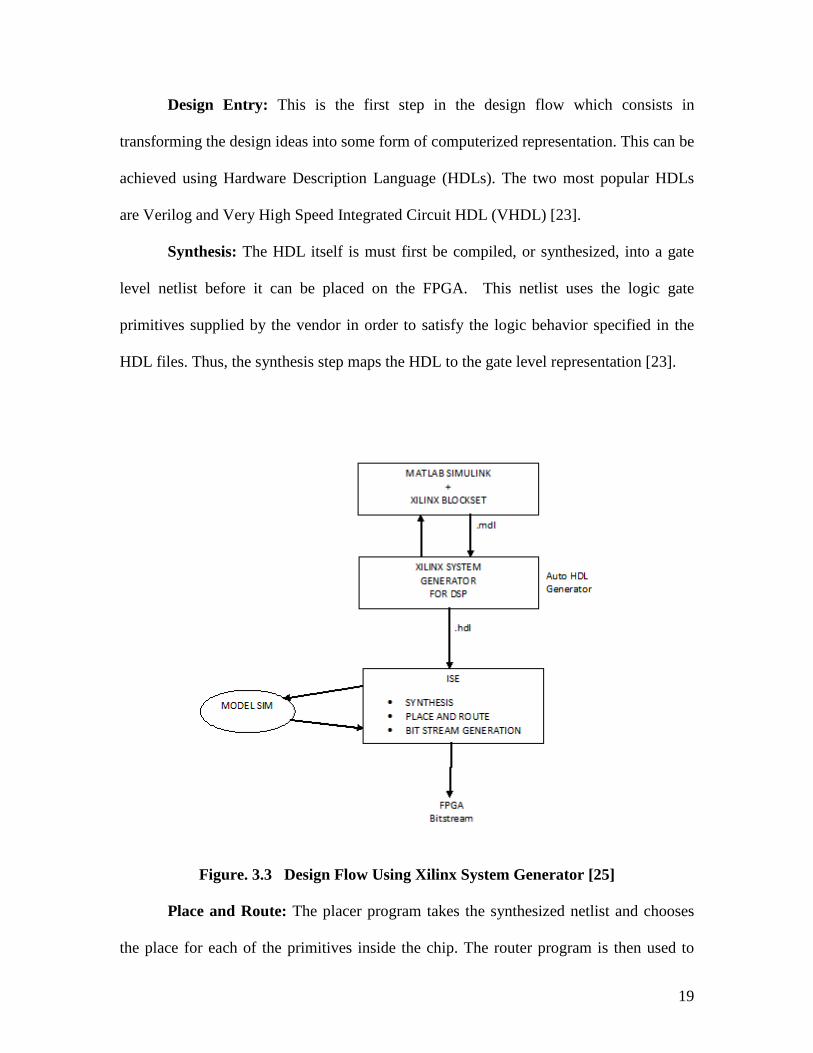
3.2 System Generator Design Flow
By using FPGAs very high throughputs can be achieved in digital signal
processing (DSP) applications. DSP application developers typically use Matlab to
develop algorithms while FPGA developers use Hardware Description Languages
(HDLs), such as Verilog and VHDL. This makes it difficult for DSP developers to
transition their applications to FPGAs.
System blocks are shared however, between DSP designers and FPGA
technology. With Xilinx, DSP designs can be implemented on FPGAs using MATLAB
and Simulink from Mathworks combined with Xilinx’s System Generator for DSP
applications. The first step of the design process is simulation of the SDR system with
Simulink. For the hardware-implementable representation of the radio, the Xilinx System
Generator block set in Simulink is used. Figure 3.3 shows the general overview of the
design flow using Xilinx system generator [24].
19
Design Entry: This is the first step in the design flow which consists in
transforming the design ideas into some form of computerized representation. This can be
achieved using Hardware Description Language (HDLs). The two most popular HDLs
are Verilog and Very High Speed Integrated Circuit HDL (VHDL) [23].
Synthesis: The HDL itself is must first be compiled, or synthesized, into a gate
level netlist before it can be placed on the FPGA. This netlist uses the logic gate
primitives supplied by the vendor in order to satisfy the logic behavior specified in the
HDL files. Thus, the synthesis step maps the HDL to the gate level representation [23].
Figure. 3.3 Design Flow Using Xilinx System Generator [25]
Place and Route: The placer program takes the synthesized netlist and chooses
the place for each of the primitives inside the chip. The router program is then used to

20
interconnect all the primitives together to satisfy the timing constraints. This can be
accomplished by Xilinx’s ISE implementation programs. The most obvious constraint for
the design is the system’s clock frequency [23].
Bit stream Generation: Placing and routing is followed by the generation of the
FPGAs programming file, called a bitstream. The design can then be downloaded into the
target FPGA [23].
3.3 Simulation with System Generator and Simulink
In this thesis, SDR algorithms are designed and simulated using Xilinx System
Generator system level tool. For timing and logic-accurate simulation of the final
hardware design, the Xilinx System Generator block sets within Simulink are used. The
Xilinx block set enables bit true and cycle true modeling and includes common blocks
such as Finite Impulse Response (FIR) filter, Fast Fourier Transform (FFT), Direct
Digital Synthesizer (DDS), multiplier and more. Below a few steps are discussed for the
processes of simulation using Simulink and System Generator [27].

21
Figure 3.4 Xilinx Gateway In, Gateway Out and System Generator Block
1. As shown in figure 3.4, Start the design by implementing Xilinx blocks in the
MATLAB Simulink program.
2. Select the Xilinx System Generator block and add it to the top of the design
model.
3. “Gateway In “and “Gateway Out” blocks are use to define the inputs and outputs
to the Xilinx design. These blocks automatically convert the double precision
floating point value used in MATLAB to the fixed point value used in the FPGA.
All the components located between these gateway blocks must be from the
Xilinx block set only.
4. The design can be simulated and the output can be verified using visual output
blocks.

22
3.4 Bitstream Generation
The System Generator system level design can be converted to a gate level
representation through the steps listed below.
Figure 3.5 System Generator Dialog Box
• The System Generator block contains the hardware setting. This is illustrated in
Figure 3.5. Xilinx XST is chosen for the Synthesis tool. HDL can be chosen as
VHDL or Verilog. In this thesis Verilog is used.
• The next step is to run the System Generator by initiating the “Generate” button.
It produces an FPGA configuration bit stream for the design that is suitable for
hardware.

23
• Once a bit stream is generated then it is downloaded on the Spartan 3E Starter Kit
board using the Xilinx ISE programming tool called Impact. [27]

24
CHAPTER 4
EXPERIMENTAL SET UP, SIMULATIONS AND RESULTS
4.1 Introduction
This chapter describes the experimental set up, simulations and results for the
different modulation techniques. Modulation techniques considered include analog
techniques such as Amplitude Modulation (AM) and digital modulation techniques such
as Amplitude Shift keying (ASK) and Binary Phase Shift Keying (BPSK). The system is
modeled and simulated using MATLAB Simulink and System Generator. The system is
then implemented on a Spartan 3E FPGA for real time measurements.
4.2 Basic Modulation Concept
Modulation is the process of converting a message into a format that can be
successfully transmitted through a medium. A sinusoid has three different parameters that
can be varied: amplitude, phase and frequency. Depending on the chosen parameter we
have modulation techniques such as amplitude modulation, phase modulation and
frequency modulation. On the receiver side the modulated sine wave is converted back to
the original information signal. In this chapter Amplitude Modulation (AM), Amplitude
Shift Keying (ASK), Binary Phase Shift Keying (BPSK) are discussed.
4.3 Amplitude Modulation (AM)
Amplitude modulation transmits information by modifying the amplitude of the
carrier signal. Let the information signal M(t) be an arbitrary waveform, called
modulating signal which is given by,
M (t) = M cos (Wm t + Φ) 4.3.1

25
Where M is the maximum value, Wm is the modulating signal frequency and Φ is
the phase angle of the modulating signal. The carrier signal is also a sine wave given by,
C(t) = C cos (Wc t + Φc) 4.3.2
Here C and Φc are arbitrary constants representing the amplitude and phase of the
carrier signal, respectively. For simplicity we consider the amplitude to be unity and
phase to be zero. The standard carrier frequency in the U.S. is in the range of the 550
KHz to 1720 KHz. Generally it is assumed that Wm << Wc.
Amplitude Modulation is created by forming the product,
Y (t) = [A + M (t)] * C (t) 4.3.3
Where A is constant and chosen to be unity in this discussion. A choice of
A being zero eliminates the carrier components. That is the Double Sideband Suppressed
Carrier (DSBSC) transmission mode. Here we choose A = 1. So it is called Double
Sideband Amplitude Modulation (DSB-AM) with carrier [14].
4.3.1 AM SDR Setup
Figure 4.1 presents the basic idea of an implementation of SDR on the Spartan 3E
Starter Kit. Peripheral Modules (PMODs) are made by Digilent in order to easily
interface peripherals to their products using a simple standard connector.
The message signal is provided from a function generator to the 12-bit ADC
housed in the peripheral board attached to the FPGA (PMOD AD1). As discussed in
Chapter 3, the bitstream file which is generated by System Generator is downloaded on
the Spartan 3E FPGA. The modulated output waveform from the 12-bit DAC peripheral
board (PMODDA2) can be observed on an oscilloscope [29].

26
Figure 4.1 Radio Set Up
4.3.2 System Generator Implementation
The simulation model for the AM modulator is shown in Figure 4.2. This diagram
is an implementation of equation 4.3.3. The message signal is given as an input to the
Gateway In block. This block converts that data from a double precision floating point
number to the Xilinx fixed point representation. The black box provides a way to include
HDL models into System Generator. The black box can be used to incorporate Verilog
files in the Simulink model. Here the first black box contains a Verilog model for the
ADC and is labeled ADC in Figure 4.2. The second black box contains a Verilog model
for the DAC and is labeled as DAC in Figure 4.2. During the hardware generation
process, the associated HDL entity is automatically wired to the other block in the design.
The output of the DAC (other black box in Figure 4.2) which contains the Verilog
module for the DAC is a 12-bit unsigned value. The Direct Digital Synthesizer (DDS)

27
compiler block is used to generate the sine wave (carrier signal), or cosine wave,
depending on the application. This capability allows users to custom build a DDS to fit
individual application needs.
Here the DDS Compiler is used to generate a 10 KHz sine wave. The output of
the DDS compiler is multiplied with constant (value of A in equation 4.3.3) using xilinx
Mult block which is shown in the Figure 4.2. Mult blocks compute the product of the data
on its two input ports. ADDSUB block performs the addition of the data on its two input
ports. The next blocks are the gain operator, constant and ADDSUB block which convert
the output of ADDSUB block to a positive 12-bit number which is a requirement of the
DAC block.

28
Figure 4.2 Simulation Model for AM Modulation
Figure 4.3 shows (a) the modulating signal, (b) the 10 KHz carrier signal and (C)
the generated modulated signal using Simulink, and Figure 4.4 presents the hardware
generated waveform. The radio design can be validated by comparing Figure 4.3 (c) and
4.4 [27, 28].

29
(a)
(b)
(c)
Figure 4.3 (a) Modulating Signal (b) Carrier Signal (c) Modulated Signal in
Simulink

30
Figure 4.4 Modulated Waveform Viewed with Oscilloscope
4.4 Amplitude Shift Keying
Figure 4.5 shows the basic block diagram for ASK modulation. In ASK the
amplitude of the carrier is changed in response to the digital data stream (information
signal). The ASK signal can be defined as,
S (t) = A1 m(t)cos(2πfc t) For Binary 1 4.4.1
S (t) = A2 m(t)cos(2πfc t) For Binary 0 4.4.2
Here A1 and A2 are two different constants representing the amplitudes of the two
carriers and m(t) is an binary input bit stream. The level of the amplitude can be used to
represent binary logic 0s and binary logic 1s. fc is the carrier frequency which is constant.
In ASK modulation a logic one is transmitted using one particular amplitude and logic
zero is transmitted by different carrier amplitude without changing the frequency. Figure
4.6 (a) shows clearly that a logic one is transmitted using a carrier of amplitude 2 and a
logic zero is transmitted by carrier of amplitude unity. Figure 4.6 (a) shows the generated
waveform for ASK. OOK is a special form of ASK modulation where a logic zero is
transmitted by carrier of amplitude zero [14].

31
Figure 4.5 Basic Block Diagram of ASK
Figure 4.6 (b) shows the waveform for OOK modulation in Simulink. Figure 4.7
shows the Hardware generated waveform for ASK Modulation. The radio design can be
validated by comparing Figure 4.6 (b) and 4.7.

32
(a)
(b)
Figure 4.6 (a) ASK Modulated Signal (b) OOK Modulated Signal in Simulink
Figure 4.7 ASK Modulated waveform viewed with Oscilloscope.

33
4.5 Binary Phase Shift Keying (BPSK)
Figure 4.8 shows the basic block diagram of the BPSK modulator. The digital
information signal (coded into digital signal) enters a multiplexer that converts the phase
of the carrier signal according to the input bit stream (information signal). Depending on
the logic condition of the input the carrier transferred to the output is either in phase or at
900 out of phase. Figure 4.8 shows clearly that a logic one is transmitted by a cosine wave
and a logic zero is transmitted by a sine wave. Figure 4.9 (a) shows the waveform for a
BPSK modulator [26]. Figure 4.9 (b) shows the Hardware generated waveform for BPSK
Modulation. The radio design can be validated by comparing Figure 4.9 (a) and 4.9 (b).
Figure 4.8 Basic Block Diagram of BPSK Modulator

34
(a)
(b)
Figure 4.9 (a) BPSK Waveform in Simulink (b) BPSK Modulated Waveform
Viewed with Oscilloscope.

35
CHAPTER 5
CONCLUSION AND FUTURE WORK
5.1 Conclusion
This thesis presents a low cost SDR platform that leverages existing educational
hardware and software. The Spartan 3E Starter Kit Board was chosen for implementing
the SDR because it is cheap and easily available. Another advantage to choosing the
Spartan 3E board is that it requires the least amount of external peripherals to implement
the radios. In this thesis just an ADC and DAC are needed as external peripherals.
This thesis used the System Generator for DSP tool developed by Xilinx for
implementing a digital signal processing application on the Xilinx FPGA platform. The
Xilinx System Generator for DSP is compatible with MATLAB Simulink. Another
advantage to choosing System Generator is that FPGA design and programming are
easily performed with its model-based approach.
The first approach in the design process was to add System Generator components
in order to simulate and implement AM modulation on the Spartan 3E Starter Board.
Results were obtained using a function generator as an input signal and an oscilloscope to
view the modulated waveform. These results were compared to simulations in System
Generator with minimal error. Based on the comparison of the results and simulations,
valid implementation was confirmed. ASK, BPSK and OOK modulation schemes were
also simulated using System Generator but not implemented on the Spartan 3E Starter
Board.

36
5.2 Suggestion for Future Work
The SDR that has been introduced in this thesis is not fully complete. Only the
baseband stage of the wireless communication system has been implemented. The other
two stages (RF and IF) have not been implemented. Therefore this can be a focus point
for future work.
This thesis could be extended by adding functionality such as channel coding, error
correction techniques, etc. In this thesis the transmitter is simulated and implemented but
not the receiver part. A typical SDR receiver involves complex techniques to recover the
frequency and phase of the transmitter’s carrier wave. The implementation of these
techniques within System Generator is left for future work.

37
REFERENCES
[1] T. Rappaport, Wireless Communication - Principle and practice, 2nd Edition.
[2] Software Defined Radio Forum. “About SDR”,
http://www.sdrforum.org/
[3] S.M.Shajedul Hasan, P. Balister, “ Prototyping a Software Defined Radio Receiver
Based on USRP and SSIE” , Technical Report No. 1, Department of Electrical &
Computer Engineering, Virginia tech, December 14,2005
[4] A. Chandrasekhar, P.Banerjee, “TDMA Implementation using GNU Radio and
USRP”, Department of Electrical and Computer Engineering, Cleveland State
University.
academic.csuohio.edu/yuc/mobile09/avi.pdf
[5] S. Naghmash, M. Ain, C. Hui,” FPGA Implemention Of Software Defined Radio
Model based 16QAM“, European Journal of Scientific Research, Vol. 35, No.2
(2009), pp.301 – 310
[6] Ke –Yu, Z. Chen, “GNU RADIO”, Department of Electrical Computer Engineering,
University of Florida, Gainesville, Florida, 2006 ,Feb ,2008.
http://www.wu.ece.ufl.edu/projects/softwareRadio/
[7] M. Hicking, “New technology facilitates true software defined radio”, Retrieved in
April 2005 from www.rfdesign.com
[8] K. Patton, “A GNU Radio Based Software – Defined Radar”, Master Thesis, Wright
State University, 2007.
[9] J. Mitola, “Software Radio Architecture,” IEEE Communication Mag, May 1995.

38
[10] H. Afshin, F. John, “Enabling Technology for Software Defined Radio”, Software
Defined Radio Technical Conference, 12 November 2002- San Diego, California.
[11] K. Jondral, “Software Defined Radio Basics and Evolution to Cognitive Radio”,
EURASIP Journal On wireless Communication and Networking 2005:3, 275 – 283
[12] Dr. Hikmat N. Abdullah, B.Sc. Hussein A. Hadi, ”Design and Implementation of
FPGA based Software Defined Radio Using Simulink HDL Coder“ CUAS Journal.
[13] J. Groati, G. Reehal, Nagarjuna, “Synthesizing FPGA Digital Modules for Software
Defined Radio”, National Aerospace and Electronics Conference, 16-18 July 2008,
Ohio.
[14] Ladimer S. Nagumey, “Software Defined Radio in the Electrical and Computer
Engineering Curriculum”, Frontiers in Education Conference, October 18-21,
2009, San Antonio, Texas.
[15] R. Schiphorst,” Demonstration of the Software – Radio Concept”, Master thesis,
University of Twente, Department Of Electrical Engineering ,Signals & System PO
Box 217, 7500 AE Enschede, the Netherlands, June 14, 2000
[16] Wipro Technologies, “Software-Defined Radio white paper,” Aug. 2002.
[17] D. Erik, P. Stefan, Communications Engineering Desk Reference, Academic press
2009-02-02.
[18] P. Mannan,”Framework for the design and implementation of Software Defined
Radio based wireless communication system”, Master Thesis to the University of
Akron, December 2005.
[19] Hunt Engineering,” The Theory of Digital down Converter”.
www.hunteng.co.uk/pdfs/tech/ddctheory.pdf

39
[20] E. Ramon, j. Carrabina, “Using FPGAs for Software Defined Radio system: a PHY
layer for an 802.15.4 transceiver”.
cephis.uab.es/resources/pdf/papers/JCRA_2005_SDR.pdf
[21] J. Serrano, Digital Signal Processing using Field Programmable Gate Arrays”, Beam
Instrumentation Workshop,2008, Geneva, Switzerland.
[22] T. Saidani, D. Dia, M. Elhamzi and R. Tourki, “Hardware Co-simulation for video
processing using Xilinx system generater”, WCE 2009 July 1 – 3 London, U.K.
[23] Xilinx,”DSP co-processing in FPGAs: Embedding high performance, low cost DSP
functions”, WP212 (v1.0) March 18, 2004.
[24] J. Ruque, D. Ruiz, C. Carrion,” Simulation and implementation of the BPSK
modulation on a FPGA Xilinx Spartan 3 xcs2004ftp256 using Simulink and the
System Generator block set for DSP/FPGA”, Group of Electricity and Electronics
System, Technical University Of Loja.
http://www.ece.unm.edu/xup/docs/collaboration/BPSK_Modulator.pdf
[26] Xilinx, “Products and Services: Design Tools,”
http://www.xilinx.com/tools/designtools.htm
[27] Math works, “Products for technical computing,”
http://www.mathworks.com/products/
[28] Digilent Inc., “Digital Designs Engineer’s Source.”
http://www.digilentinc.com/