Embed Size (px)
Citation preview

——————————————————————————————————————

[International Journal of Information Technology (IJOIT Vol-‐1 Issue-‐4 August 2017]
1
IMPLEMENTATION AND DESIGNING OF LOW POWER SR FLIP-FLOP USING 45NM CMOS
TECHNOLOGY S V S V PRABHU DEVA KUMAR1, PAGADALA VENKAT2, LOKESH NAYINI3
1 Research scholar,ITM university,
Gwalior,Madya Pradesh,India. [email protected]
2 Research scholar,ITM university,
Gwalior,Madya Pradesh,India. [email protected]
3 Research scholar,Amrita school of Engineering,
Bengaluru,Karnataka,India [email protected]
Abstract The design of low-power devices is currently an important area of research due to an increase in demand for portable devices. Since the MOS device is widespread, there is a great need for circuits to consume less power, especially for portable and handheld devices. A memory element consumes 70 percent of the total power in an integrated circuit. As flip-flop is the primary place of memory elements to use on any portable device, a wide attention to reduce energy consumption flip-flop will help reducing energy consumption in a large IC. In this paper, we designed a flip-flop with CMOS logic; It consumes less energy than conventional gates designed. Switching transistors occurs when applied input clock is applied. Proposed SR flip-flop synchronization, 0.7V power dissipation transient analysis and SR flip-flop different applications. This flip-flop is implemented using 45 nm in virtuoso cadence. Keywords: SR Flip-Flop, Operation, Designing, Low Power, CMOS Technology.
1. Introduction
Sequential circuits are logic circuits whose production in any aspect of this moment depends not only on the input current, but the problems of the past. Sequential circuits are of two types: (i) clocked and (ii) unclocked. The simplest type of sequential circuit is a memory cell in these two states. It can be 1 or 0. These two circuits are called sequential flip-flop state states from one state to another and vice versa. Flip-flops are used as memory elements which are the basic elements of an integrated circuit. They are used in many applications such as data storage registering in parallel flow, counter and frequency division, etc ... Computers and machines utilize flip-flop for your memories. A combination of the number of flip-flops can cause a certain amount of memory. Flip-flop is constructed using logic gate, which in turn is constituted by transistors. Flip-flops are the main elements of electronic memory devices. Each flip-flop can store a given one. The SR flip-flop, also known as SR Latch can be considered as one of the possible most basic sequential logic circuits. One of these "set" devices (ie output = "1") and labeled S and other "reset" devices (ie, this simple flip-flop is in fact a memory device bistable with a little ' Having two inputs, output = "0"), labeled R.
Then, SR description means "Set reset." Resetting the flip-flop reset input in its initial state at Q output will be a logic level of "1" or "0" depending on the state of the set / reset.
2. Working of SR Flip Flop Model:
Flip-flop SR is commonly used flip-flop. It is also known as a set-reset flip-flop. Notice that when inputs S = "1" and R = "1" Q and Q’ can be either logical levels "1" or "0" output, depending on state of S or R input, given input . Therefore, the condition of S = R = "1" does not change the status of output Q and Q’.
——————————————————————————————————————

[International Journal of Information Technology (IJOIT Vol-‐1 Issue-‐4 August 2017]
2
However, the input state S = "0" and R = "0" is an undesirable condition or invalid and should be avoided. The condition S = R = "0" causes both output Q and Q’ together to be high logic level "1" when reverse is usually Q. Q is losing the result of the check is that flip-flop Q and Q’ , And where the two inputs are now switched "high" after logical condition "1", the flip-flop becomes unstable and changes in a state of unknown data based on imbalance as shown in the pattern reduction Penalty.
Figure 1 SR flip-flopimplementation using transistor level logic
Table 1 SR Flip-flop truth table
S R Q Q’
0 0 0 1
0 0 1 0
0 1 0 1
1 0 1 0 1 1 0 0
If S= 0;R=1 then Q = 0; Q’ = 1 so flip flop is reset. If S = 1;R=0Q = 1; Q’ = 0 so flip flop is set.
3.Operation of SR Flip Flop:
3.1.Set State of SR Flip Flop:
Consider the circuit shown above. If R input is logic level "0" (R = 0) and S input is logic level "1" (S = 1), the NAND gate has at least one inputs in logic "0" Output Q should be a logical value "1" ( NAND gate principle). Output Q "A" input is also restored, then both input X NAND gate is at logic level "1" and then the Q output should be no logic level "0".
——————————————————————————————————————
[International Journal of Information Technology (IJOIT Vol-‐1 Issue-‐4 August 2017]
3
He leads the NAND gate again. If input R reset R changes state and goes to HIGH logic "1" and S remains high at a logic level of "1", NAND gate is now Y ,R = "1" and B = "0". As one of its inputs is still at logic level "0" Q output remains highly logical "1" and has no state change. Therefore, it is said that the flip-flop circuit is "register" or "set" Q = "1" and Q = "0".
3.2.Reset State of SR Flip Flop:
In the second static state, Q is at the level "0" (not Q = "0") of the inverse Q output is logic level "1" (Q = "1") and is given by R = "1 'And S =' 0 'When the X port is one of the inputs in the logic "0" Q output must be equal to the logic value "1" (NAND gate principle.) The Q output at input "B" Returned, so that both NAND gate inputs are logical "1", therefore, Q = "0".
If the S input set is now changing its state from the logic "1", the input R in logical "1", the Q output is still low still at logic level "0" and there is no state change. Therefore, the state of the "reset" of the flip-flop circuit also has been blocked and may specify the action to "set / reset" in the following fact tables.
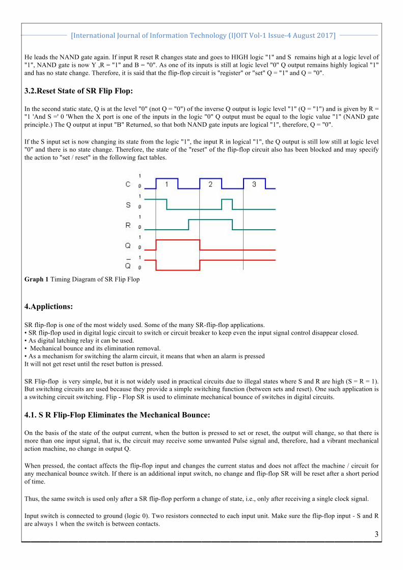
Graph 1 Timing Diagram of SR Flip Flop
4.Applictions:
SR flip-flop is one of the most widely used. Some of the many SR-flip-flop applications. • SR flip-flop used in digital logic circuit to switch or circuit breaker to keep even the input signal control disappear closed. • As digital latching relay it can be used. • Mechanical bounce and its elimination removal. • As a mechanism for switching the alarm circuit, it means that when an alarm is pressed It will not get reset until the reset button is pressed.
SR Flip-flop is very simple, but it is not widely used in practical circuits due to illegal states where S and R are high (S = R = 1). But switching circuits are used because they provide a simple switching function (between sets and reset). One such application is a switching circuit switching. Flip - Flop SR is used to eliminate mechanical bounce of switches in digital circuits.
4.1. S R Flip-Flop Eliminates the Mechanical Bounce:
On the basis of the state of the output current, when the button is pressed to set or reset, the output will change, so that there is more than one input signal, that is, the circuit may receive some unwanted Pulse signal and, therefore, had a vibrant mechanical action machine, no change in output Q.
When pressed, the contact affects the flip-flop input and changes the current status and does not affect the machine / circuit for any mechanical bounce switch. If there is an additional input switch, no change and flip-flop SR will be reset after a short period of time.
Thus, the same switch is used only after a SR flip-flop perform a change of state, i.e., only after receiving a single clock signal.
Input switch is connected to ground (logic 0). Two resistors connected to each input unit. Make sure the flip-flop input - S and R are always 1 when the switch is between contacts.
——————————————————————————————————————

[International Journal of Information Technology (IJOIT Vol-‐1 Issue-‐4 August 2017]
4
You can generate another circuit with NOR SR FLOP.
Figure 2 SR Elimination of Mechanical bounce
Input switch is connected to logic 1. Two resistors connected between input disconnections. Make sure the flip-flop input S and R are always 0 when the switch is between contacts a and b.
Integrated Circuits commonly used to eliminate mechanical switch bounce are MAX6816 - single MAX6817 – dual input, MAX6818 – octal input switch de-bouncer IC’s. Integrated circuits contain the necessary configuration of SR flip-flop.
5. Stimulated Results:
As we designed the energy-saving flip-flop logic levels of transistor SR compared to combinatorial designs, and responded more specifically to working with other technologies. We implements this technology 45nm technology.
——————————————————————————————————————

[International Journal of Information Technology (IJOIT Vol-‐1 Issue-‐4 August 2017]
5
Figure 3 Transistor level logic of SR Flip-flop using 45nm technology
——————————————————————————————————————

[International Journal of Information Technology (IJOIT Vol-‐1 Issue-‐4 August 2017]
6
Graph2 The Transient Response of SR flip flop.
6. Conclusion:
In this article, SR flip-flop has been implemented using more number of transistors. In low-power applications, and the area of the device power consumption is the key to prefer a drawing to other technological innovation models. Full-fledge measurement SR flip-flop shows better performance in terms of power dissipation and illustrations described here.
——————————————————————————————————————
[International Journal of Information Technology (IJOIT Vol-‐1 Issue-‐4 August 2017]
7
References
[1] rving, Thurman A.; Shiva, Sajjan G.; Nagle, H. Troy (March 1976). "Flip-Flops for Multiple-Valued Logic". Computers, IEEE Transactions on. C–25 (3): 237–246 [2] “Design and Implementation of S R Flip flop for Efficient power using CMOS 90nm Technology” Anjana S, Rajesh Mehra. International Journal of Scientific Research Engineering & Technology (IJSRET), ISSN 2278 – 0882 Volume 4, Issue 5, May 2015 [3] Seelam Vasavi Sai Viswanada Prabhu Deva Kumar et al.2017, “Implementation of Low Power D-Flipflop Using 45nm Cmos Technology”. Int J Recent Sci Res. 8(6), pp. 17729-17732. [4] N. Nishanth, B.Sathyabhama, “Design of Low Power Sequential Circuit Using Clocked Pair Shared Flip flop”, 2013 IEEE International Conference on Emerging Trends in Computing, Communication and Nanotechnology (ICECCN 2013). [5] “Low Power Design of Sr Flip Flop Using 45nm Technology” Pratiksha Gupta, Dr. Rajesh Mehra. IOSR Journal of VLSI and Signal Processing (IOSR-JVSP) Volume 6, Issue 2, Ver. I (Mar. -Apr. 2016), PP 54-57 e-ISSN: 2319 – 4200, p-ISSN No. : 2319 – 4197 [6] Paneti Mohan & P.C Praveen Kumar, “A Modified SR Flip- Flop with Deep Submicron Technology for Electronic Systems”, International Journal of Advanced Electrical and Electronics Engineering, (IJAEEE), 2013. [7] Pushpasaini ,Rajeshmehra “Leakage reduction power in CMOS VLSI Circuit” International Journal and Computer Application (IJCA), Volume-8,October 2012. [8] Mostafa H., Anis M., Elmasry M., “Comparative Analysis of Timing Yield Improvement under Process Variations of Flip-Flop Circuits”, IEEE Computer Society Annual Symposium on VLSI (ISVLSI '09), 2009, pp. 133 - 138. [9] Massimo Alioto, “Physical Design Aware Selection of Energy-Efficient and Low-Energy Nanometre Flip-Flops”, 22nd international conference on microelectronics ©2009 IEEE [10] IEEE Electronic Devices letters vol-29 no,26June 2008 A Novel SR latch device Realized by Integration of Three Terminal Ballistic Junctions in InGaAs/InP Jie Sun, Danniel Wallin, Ivan Maximov and H.Q.Xu
——————————————————————————————————————

[International Journal of Information Technology (IJOIT Vol-‐1 Issue-‐4 August 2017]
8
Author(s) Profile
Seelam Vasavi Sai Viswanada Prabhu Deva Kumar born in “Chintalapudi” a city in Andhra Pradesh, India on 15th June 1996. He is pursuing B.Tech in Electronics & Communication Engineering from Institute of Technology & Management University (ITMU), Gwalior in 2014-2018 and area of interest in LED Fabrication and Designing, Embedded Systems, Low Power VLSI Design, Modeling, and CMOS based memory design, Circuits for future VLSI Technology, Digital Design & FPGA Implementation.
He worked as an Intern in Fuzinix Infotech Pvt. Ltd. and SION Semiconductors Pvt. Ltd. Seelam Vasavi Sai Viswanada Prabhu Deva Kumar is authored/Co-authored published few research papers in peer reviewed international journals.
Pagadala Venkat born in “Bapatla” a city in Andhra Pradesh, India on 15th January
1997. He is pursuing B.Tech in Electronics & Communication Engineering from
Institute of Technology & Management University (ITMU), Gwalior in 2014-2018 and
area of interest in FPGA Chip Design, Embedded Systems, VLSI Technology, Digital
Circuit Design &Analog Circuit Design. Heworked as an Intern in Electronics
Corporation of India Ltd.
Lokesh Nayini born in “kodada” a city in Andhra Pradesh, India on 19th September
1996. He is pursuing B.Tech in Electronics & Communication Engineering from Amrita
University, benguluru in 2014-2018 and area of interest in FPGA chip design and PCB
design, VLSI Technology, Digital &Analog Circuit Design. He worked as an Intern in
SION Semiconductors Pvt. Ltd. and WHR power plant in Penna cement industry.
——————————————————————————————————————