Embed Size (px)
Citation preview

Impedance Matching of Transmission LinesKirk T. McDonald
Joseph Henry Laboratories, Princeton University, Princeton, NJ 08544(July 20, 2005; updated October 4, 2014)
1 Problem
This problem considers several ways of “matching” two transmission lines such that a wavepropagates from the first to the second line without reflection at the junction.
The related problem of “matching” a transmission line to a load is also considered tosome extent.
In this problem, a transmission line is a device consisting of two parallel conductors suchthat TEM (transverse electromagnetic) waves can be propagated. Examples of transmissionlines include coaxial cables, and simple 2-wire (Lecher) lines.
Take the lines to lie along the x axis. Then, the two conductors carry currents I(x, t)and −I(x, t), waves of angular frequency ω propagating in the +x direction have the form
I(x, t) = I+ cos(kx− ωt) = Re(I+ei(kx−ωt)), which we abbreviate as I = I+ei(kx−ωt), (1)
where i =√−1, k = 2π/λ is the wave number and ω/k is the wave velocity.1,2 Similarly,
waves propagating in the −x direction have the form
I(x, t) = I−ei(−kx−ωt). (2)
A voltage difference V (x, t) exists between the two conductors, which is related to thecurrent in the conductors according to
V = IZ, (3)
where Z is the impedance of the transmission line. A sign-convention is required for properuse of eq. (3); we say that V+ = I+Z for waves propagating in the +x direction, whileV− = −I−Z for waves propagating in the −x direction.
If waves are propagating in both directions along a transmission line, then the voltage isrelated to the current by
V = V+ + V− = (I+ − I−)Z. (4)
1If the conductors are surrounded by vacuum, the wave velocity is c, the speed of light. If the conductorsare embedded in dielectric and/or permeable media with (relative) dielectric constant ε and (relative) per-meability μ, the wave velocity is c/n where n =
√εμ is the index of refraction. In this case, the wave number
can be written k = nω/c, and the wave length is λ = c/2πnω. If several different sections of transmissionline are present, they can have different indices, wave numbers and wave lengths for waves of a given angu-lar frequency ω. While we ignore this possibility in the present note, it could be accommodated by minorchanges in notation.
2If the currents on the two conductors are not equal and opposite, then their average (I1 +I2)/2 is calledthe common mode current. This case is generally undesirable as it involves transfer of energy to and fromthe environment of the transmission line. We do not consider common mode currents in this problem.
1

The transmission line may be assumed to operate in vacuum (rather than in a dielectricthat can support leakage currents). The capacitance and inductance per unit length alongthe line are C and L, respectively. The resistance per unit length along the conductors isnegligible.
(a) Reflection Due to an Impedance Mismatch.
Suppose that two transmission lines are directly connected to each other, as illustratedbelow for coaxial cables of impedances Z1 and Z2.
3
Show that the power transmitted into line 2 is given by
P2 =4Z1Z2
(Z1 + Z2)2P1, (5)
where P1 is the power in line 1 that is incident on the junction. How much power isreflected back down line 1?
(b) Reflection Due to a Complex Load Impedance.
Generalize part (a) to include the case that Z2 is a complex load impedance, rather thana transmission line with a real impedance. Show that the ratio of the total voltage tothe total current in the input coaxial cable is real for a set of positions along the cable,which permits matching at these points using the techniques considered in the rest ofthis problem. A graphical representation of this insight uses the so-called Smith chart[1]. For discussion of impedance matching of the voltage source to the transmissionline, see [2].
(c) Impedance Matching via Resistors.
Show that there will be no reflected wave from an incident in line 1 if an appropriateresistor is placed at the junction. The case that Z2 > Z1 and Z2 < Z1 must be dealtwith separately if only a single resistor is to be used. Hence, this scheme for matchingworks only when the waves are incident from line 1.
Because the resistors dissipate energy, the transmitted power is less than the inci-dent power. Further, the resistive impedance matching scheme works only for wavestransmitted in one direction.
3The figure includes a load resistor of value R = Z2 at the end of transmission line 2. Without sucha load resistor there would be reflections off the end of line 2, and the analysis would need to be modifiedaccordingly.
2

(d) A λ/4 Matching Section.
Show that the power can be transmitted without loss at a particular frequency ω from atransmission line of impedance Z1 into one of impedance Z2 if the junction consists of apiece of transmission line of length λ/4 and impedance Z0 =
√Z1Z2. This prescription
is familiar from antireflection coatings on optical lenses.
This scheme works for waves transmitted in either direction, but requires a preciseimpedance for the matching section, which may not be readily available in practice.
Show also that a transmission line of impedance Z1 could be matched into a complexload Z2 = R+iX with an appropriate length l �= λ/4 of transmission line of impedanceZ0, provided that R �= Z1.
(e) A “λ/12” Matching Section.
Show that power can be transmitted without loss at a particular frequency ω from atransmission line of impedance Z1 into one of impedance Z2 if the transition consistsof two pieces of transmission line of equal lengths l ≈ λ/12 and impedance Z2 and Z1,as sketched below.
This scheme works for waves transmitted in either direction, and can be built usingonly pieces of the two transmission lines of interest. However, the matching is optimalonly at a single frequency.
The “λ/12” matching scheme was invented by P. Bramham in 1959 [3]. In 1971,F. Regier gave a generalization that permits matching a transmission line of (real)impedance Z1 to a complex load impedance Z = R+ iX, where R is the load resistanceand X is the load reactance [5].
Given impedances Z, Z1 and Z2, deduce the lengths l1 and l2 of the matching sections.
When Z = Z2 is real, then the lengths of the matching sections are l1 = l2 =(λ/4π) cos−1[(Z2
1 + Z22 )/(Z1 + Z2)
2], which is close to λ/12 = 0.08333λ as shown inthe figure below (from [4]).
3

(f) Impedance Matching via a Flux-Linked Transformer.
Show that transmission lines 1 and 2 can be matched if each line is attached to a smallcoil with N1 and N2 turns, respectively (as shown on the next page), where N1/N2 =√
Z1/Z2. All of the magnetic flux created by the current coil 1 should be linked by coil2, and vice versa, for ideal transformer action. You may ignore the internal resistancesand capacitances of the transformer windings. Even with these idealizations, showthat a transmission-line analysis predicts a reflected power that varies as 1/ω2 (at highfrequency), so that a flux-linked transformer has poor performance at low frequency.
To maximize the flux linkage in practice, it is advantageous to wind the two coilsaround a ring or “core” of a high-permeability magnetic material, such as a ferrite.See, for example, [6]. However, the performance of magnetic materials is limited atvery high frequencies, so a ferrite-based, flux-linked, impedance-matching transformerhas only a finite bandwidth.
Lenz’ law indicates that the induced current in line 2 will have the opposite sign tothat in line 1. Hence, the voltage in lines 1 and 2 are reversed at their junction, andwe speak of an inverting transformer. A noninverting transformer could be built usingtwo ferrite cores, as shown in the figure below.
A matching transformer can be constructed with no metallic connection between theconductors of line 1 and those of line 2. In this case we speak of an isolation transformer,particularly when the impedance of lines 1 and 2 is the same.
There is some special terminology associated with isolation transformers, based on theconcepts of balanced and unbalanced transmission lines. In principle, a balanced trans-mission line is one in which only a TEM wave propagates, and so the currents on its
4

two conductors are equal and opposite at each point along the line. Any transmissionline can become unbalanced due to coupling with electromagnetic fields in its environ-ment, but connecting one of the conductors to an electrical “ground” also unbalancesthe line.4 An isolation transformer connected to an unbalanced line 1 can result in line2 being balanced, and therefore the name balun (balanced-unbalanced) is sometimesgiven to isolation transformers.
(g) The Transmission-Line Transformer of Guanella.
In 1944, Guanella [7] suggested a device that can match a (primary) transmission lineof impedance ZP to a (secondary) line of impedance ZS = 4ZP using two intermediatepieces of transmission line of impedance ZI = 2ZP , as shown in the figure below.
Verify the desired functionality of this circuit, supposing that the intermediate segmentsof transmission lines are long enough that a true TEM wave propagates in them. Thishas the effect that the voltages at the two ends of these segments are isolated from oneanother, because the integral
∫E· dl along the line vanishes for a TEM mode.
For the above condition to hold, the intermediate segments need to be a wavelengthor more long, which may be inconvenient in practice. Guanella suggested that shortintermediate segments could be used if their conductors were wound into inductivehelices, rather than being simple straight wires. When his scheme was later applied tocoaxial cables, the inductive isolation was provided by looping the coax cable through aferrite core. This improves the low-frequency response of the device without changingits basic principle.
Guanella’s device has come to be known as a transmission-line transformer even though itdoes not involve any classic transformer action as first discovered by Faraday. BecauseGuanella’s transmission-line transformer provides a measure of isolation between thevoltages at its two ends, it also serves as a balun. In some applications, the isolation ismore important than the impedance match.
Many variants of the transmission-line transformer have been conceived [8, 9, 10]. Forexample, a piece of coax cable that passes through a ferrite core is called by some a1:1 transmission-line transformer [11], although it might be more correct to call it abalun.
4If the currents on the two conductors of a transmission line are labeled Ia and Ib, then we can write
Ia =Ia + Ib
2+
Ia − Ib
2≡ Icommon + ITEM, Ib =
Ia + Ib
2− Ia − Ib
2= Icommon − ITEM, (6)
where the antisymmetric currents are associated with TEM wave propagation, and the symmetric currentsare often called common mode currents. Note that the symbol ≡ means 1“is defined to be”.
5

A more nontrivial variant is obtained if a second coaxial cable is attached to the first(the one that passes through the ferrite core), with the conductors of the two cablescross connected as shown below. In this case we obtain a 1:1 inverting transmission-linetransformer.
Show that if m intermediate segments of impedance ZI = 2ZP are used instead two,shorting the inner and outer conductors of adjacent cables at their output ends, theresulting transmission-line transformer makes a 1 : m2 impedance match.
If the intermediate transmission lines are shorted to one another at appropriate placesat their input ends as well as their output ends, additional transformer ratios may beobtained. For example, if four intermediate sections of impedance ZI = (5/3)ZP areconnected as shown on the next page, we can make a match to a secondary line ofimpedance ZS = (25/9)ZP .
2 Solution
(a) Reflection Due to an Impedance Mismatch.
We first deduce the wave equations for current and voltage in a transmission line, andthen relate this to the concept of impedance.
To illustrate the steps in deducing the wave equation, we use figures based on a 2-wiretransmission line. Referring to the sketch below and recalling that L is the inductanceper unit length of the “loop” formed by the two lines, Kirchoff’s rule for the circuit oflength dx shown by dashed lines tells us
V (x) − V (x + dx) − (Ldx)∂I
∂t= 0, or − ∂V
∂x= L
∂I
∂t. (7)
6
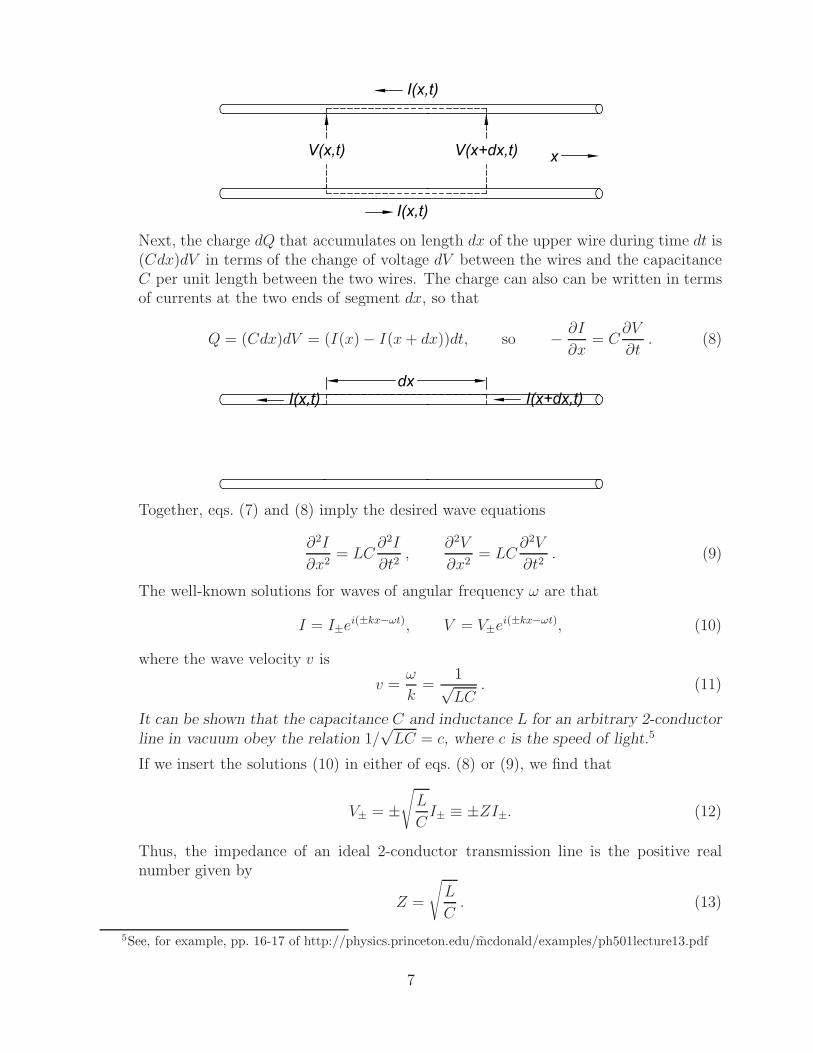
Next, the charge dQ that accumulates on length dx of the upper wire during time dt is(Cdx)dV in terms of the change of voltage dV between the wires and the capacitanceC per unit length between the two wires. The charge can also can be written in termsof currents at the two ends of segment dx, so that
Q = (Cdx)dV = (I(x)− I(x + dx))dt, so − ∂I
∂x= C
∂V
∂t. (8)
Together, eqs. (7) and (8) imply the desired wave equations
∂2I
∂x2= LC
∂2I
∂t2,
∂2V
∂x2= LC
∂2V
∂t2. (9)
The well-known solutions for waves of angular frequency ω are that
I = I±ei(±kx−ωt), V = V±ei(±kx−ωt), (10)
where the wave velocity v is
v =ω
k=
1√LC
. (11)
It can be shown that the capacitance C and inductance L for an arbitrary 2-conductorline in vacuum obey the relation 1/
√LC = c, where c is the speed of light.5
If we insert the solutions (10) in either of eqs. (8) or (9), we find that
V± = ±√
L
CI± ≡ ±ZI±. (12)
Thus, the impedance of an ideal 2-conductor transmission line is the positive realnumber given by
Z =
√L
C. (13)
5See, for example, pp. 16-17 of http://physics.princeton.edu/mcdonald/examples/ph501lecture13.pdf
7

The time-average power carried by either the + or the − wave is given by
P± =Re(V±I�
±)
2=
V±I±2
= ±ZI2±
2= ±V 2
±2Z
, (14)
where the sign of the power indicates the direction of propagation of the wave alongthe x axis.
After these lengthy preliminaries, we return to the question of the power transmittedacross the junction between transmission lines of impedances Z1 and Z2.
Assuming that the incident wave arrives from x = −∞ on line 1, this wave is describedby current and voltage I1+ and V1+ = I1+Z1. At the junction with line 2, the incidentwave splits in to a transmitted wave described by current and voltage I2+ and V2+ =I2+Z2, and a reflected wave described by current and voltage I1− and V1− = −I1−Z1.
Both current and voltage are continuous at the junction, so we have
V2+ = V1+ + V1−, (15)
I2+ = I1+ + I1−. (16)
Using eq. (12) to eliminate the voltages in favor of the currents, eq. (15) becomes
I2+Z2
Z1= I1+ − I1−. (17)
Solving eqs. (16) and (17) we find
I1− =Z1 − Z2
Z1 + Z2I1+, I2+ =
2Z1
Z1 + Z2I1+. (18)
So, whenever there is an impedance mismatch, i.e., whenever Z1 �= Z2, there is areflected wave created by the junction.
Using eq. (14) we calculate the reflected and tranmitted power to be
P1− =(
Z1 − Z2
Z1 + Z2
)2
P1+, P2+ =4Z1Z2
(Z1 + Z2)2P1+. (19)
These powers obey P1− + P2+ = P1+, which also follows from conservation of energyat the junction, which has been assumed to be lossless.
(b) Reflection Due to a Complex Load Impedance.
The analysis of eqs. (15)-(18) does not actually depend on the assumption that theimpedances Z1 and Z2 are real numbers. For the case of complex impedances, eq. (14)becomes P± = ±Re(Z) |I±|2 /2, so that the generalization of eq. (19) for Z1 real butZ2 complex is
P1− =
∣∣∣∣Z2 − Z1
Z2 + Z1
∣∣∣∣2
P1+, P2+ =4Z1 Re(Z2)
|Z2 + Z1|2P1+. (20)
8

The first of eq. (18) is often rewritten as
Ir =1 − Z2/Z1
1 + Z2/Z2Ii =
1 − z
1 + zIi ≡ −γIi, (21)
where subscript i means incident, subscript r means reflected, z = Z2/Z1 is the normal-ized load impedance, and
γ =z − 1
z + 1(22)
is the complex voltage reflection coefficient, since Vr = γVi according to the sign con-vention (12). We note that
z =1 + γ
1 − γ. (23)
At a point x < 0 on line 1, the total voltage is6
V1(x, t) = V1+ei(kx−ωt) + V1−ei(−kx−ωt) = Z1I1+(eikx + γe−ikx)e−iωt, (26)
and the total current is
I1(x, t) = I1+ei(kx−ωt) + I1−ei(−kx−ωt) = I1+(eikx − γe−ikx)e−iωt, (27)
We introduce the complex, position-dependent impedance Z(x) defined so that V1(x, t) =I1(x, t)Z(x),
Z(x) = Z11 + γe−2ikx
1 − γe−2ikx. (28)
If line 1 were terminated at position x by a load of impedance Z(x), the reflected wavewould be just the same as when the line is terminated at x = 0 by impedance Z2.
As a check, note that Z(0) = Z1(1 + γ)/(1 − γ) = Z1z = Z2 using eq. (23).
If Z(x) is real, then a “match” could be made at position x using techniques appropriatefor real, i.e., purely resistive, loads as considered in parts (c) and (d). From eq. (28)
6A practical diagnostic of the modulated traveling wave (26) can be obtained by placing a “square-law”detector across the transmission line at position x, which measures the DC root-mean-square (rms) voltage,
Vrms(x) =
√Re(V1V
�1 )
2= V1+
√1 + |γ|2 + 2 |γ| cos(φ − 2kx)
2, (24)
where we write the complex reflection coefficient (22) as γ = |γ| eiφ. The maxima and minima of Vrms(x)occur at values of x separated by λ/4 and have magnitudes V1+(1±|γ|)/√2. The ratio of the maximum rmsvoltage to the minimum is called the VSWR,
VSWR =1 + |γ|1 − |γ| . (25)
VSWR is an acronym for voltage standing wave ratio, although strictly speaking the waveform (26) is not apure standing wave unless γ = 1. An applet that illustrates the waveform (26) for real values of γ is availableat http://www.bessernet.com/Ereflecto/tutorialFrameset.htm Note that
√2Vrms(x) is the envelope of the
waveform V1(x, t).
9
we see that Z(x) will be real if γe−2ikx is real also. After some algebra, we find thedesired value(s) of x to be
x =λ
4πtan−1
(2Im(z)
1 − |z|2)
=λ
4πtan−1
(2Z1Im(Z2)
Z21 − |Z2|2
)=
λ
4πtan−1
(2Z1X2
Z21 − R2
2 − X22
),
(29)where we write Z2 = R2 + iX2. Recall that we desire x to be negative, so we rewriteeq. (29) as
− x =λ
4πtan−1
(2Z1X2
R22 + X2
2 − Z21
), (30)
so that we can use the smallest positive value of the arctangent as our solution.
As expected, if the load reactance X2 is zero, we obtain x = 0 as the position closestto the load at which the impedance Z(x) is real.
The real value of the impedance Z(x) for x given by eq. (30) is
Z(x) = Z1
√Z2
1 + R22 + X2
2 + 2Z1R2 −√
Z21 + R2
2 + X22 − 2Z1R2√
Z21 + R2
2 + X22 + 2Z1R2 +
√Z2
1 + R22 + X2
2 − 2Z1R2
. (31)
If X2 = 0 then according to eq. (31), Z(x) = R2 as expected.
The Smith Chart.
Before computers and pocket calculators were common, P.H. Smith [1] gave a graphicalmethod for finding the values of x for which Z(x) is real, as well as the real values forZ(x).
Converting eq. (28) to a normalized impedance, we write
z(x) =1 + γe−2ikx
1 − γe−2ikx=
z + i tan(kx)
1 + iz tan(kx), (32)
using eq. (22). We can also define a complex, position-dependent reflection coefficientaccording to
γ(x) =z(x) − 1
z(x) + 1= γe−2ikx = |γ| ei(φγ−2kx). (33)
The complex, position-dependent reflection coefficient γ(x) moves in a circle of radius|γ| ≤ 1 on the complex plane, and completes one clockwise rotation around this circlewhen x increases by λ/2. This insight is represented graphically on a so-called Smithchart, with is a plot of the complex reflection coefficient γ = u+ iv on the complex u-vplane.
10
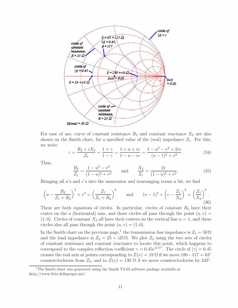
For ease of use, curve of constant resistance R2 and constant reactance X2 are alsoshown on the Smith chart, for a specified value of the (real) impedance Z1. For this,we write
z =R2 + iX2
Z1=
1 + γ
1 − γ=
1 + u + iv
1 − u − iv=
1 − u2 − v2 + 2iv
(u − 1)2 + v2. (34)
Thus,R2
Z1=
1 − u2 − v2
(1 − u)2 + v2and
X2
Z1=
2v
(1 − u)2 + v2. (35)
Bringing all u’s and v’s into the numerator and rearranging terms a bit, we find
(u − R2
Z1 + R2
)2
+ v2 =(
Z1
Z1 + R2
)2
and (u − 1)2 +(v − Z1
X2
)2
=(
Z1
X2
)2
.
(36)These are both equations of circles. In particular, circles of constant R2 have theircenter on the u (horizontal) axis, and these circles all pass through the point (u, v) =(1, 0). Circles of constant X2 all have their centers on the vertical line u = 1, and thesecircles also all pass through the point (u, v) = (1, 0).
In the Smith chart on the previous page,7 the transmission line impedance is Z1 = 50Ωand the load impedance is Z2 = 25 + i25Ω. We plot Z2 using the two sets of circlesof constant resistance and constant reactance to locate this point, which happens tocorrespond to the complex reflection coefficient γ = 0.45ei117◦. The circle of |γ| = 0.45crosses the real axis at points corresponding to Z(x) = 19 Ω if we move 180−117 = 63◦
counterclockwise from Z2, and to Z(x) = 130 Ω if we move counterclockwise by 243◦.
7The Smith chart was generated using the Smith V2.03 software package available athttp://www.fritz.dellsperger.net/
11

The corresponding distances along the coaxial cable are x = (λ/2)(63/360) = 0.05λ,and x = (λ/2)(243/360) = 0.34λ.
We leave it to the reader to judge whether the graphic construction is more or lessconvenient than using the algegbraic relations (30)-(31). Either way, one could “match”the complex load impedance Z2 to the coaxial cable of impedance Z1 by cutting intothe cable at position x and adding an appropriate matching resistor either in seriesor parallel, depending on whether Z(x) is greater or less than Z1, as discussed in thefollowing section.
(c) Impedance Matching via Resistors.
According to eq. (18) or (19), there will be no reflected wave at a junction if the totalimpedance beyond the junction is the same as that before the junction.
So, if Z2 < Z1, placing a resistor of value R = Z1 − Z2 in series with line 2 brings theimpedance beyond the junction to Z1, and no reflection will occur.
The currents in both lines are equal: I1+ = I2+. However, the series resistance reducesthe voltage in line 2 to
V2+ = I2+Z2 = I1+Z2 =Z2
Z1
V1+. (37)
Hence, the transmitted power is
P2+ =V2+I2+
2=
Z2
Z1
V1+I1+
2=
Z2
Z1P1+ (Z2 < Z1). (38)
Similarly, if Z2 > Z1, then the impedance beyond the junction can be reduced to Z1
by adding a resistor in parallel (i.e., between the two conductors at the junction) ofvalue R given by
1
R=
1
Z1− 1
Z2, so that R =
Z1Z2
Z2 − Z1. (39)
In this case the voltages on the two lines are equal, V2+ = V1+, while the currents arerelated by
I2+ =V2+
Z2=
V1+
Z2=
Z1
Z2I1+, (40)
and the transmitted power is only
P2+ =V2+I2+
2=
Z1
Z2
V1+I1+
2=
Z1
Z2
P1+ (Z2 > Z1). (41)
(d) A λ/4 Matching Section.
We suppose that the transmission line of impedance Z1 occupies the region x < 0, thetransition section of impedance Z0 runs from x = 0 to x = l, and the line of impedanceZ2 extends over the region x > l.
12
The incident wave in line 1 moves in the +x direction, and we desire no reflected wavethis line. The matching section can support waves in both direction, while the wavein line 2 should move only in the +x direction.
We can write the various waves as8
V1+ = V1+ei(kx−ωt) = I1+Z1, (42)
V0+ = V0+ei(kx−ωt) = I0+Z0, (43)
V0− = V0−ei(−kx−ωt) = −I0−Z0, (44)
V2+ = V2+ei(kx−ωt) = I2+Z2. (45)
Continuity of the current and voltage at the junction x = 0 tells us that
I1+ = I0+ + I0−, (46)
V1+ = V0+ + V0−. (47)
Eliminating voltage in favor of current in eq. (47), we have
I1+Z1
Z0= I0+ − I0−. (48)
Solving eqs. (46) and (48), we find the currents in the matching section to be
I0± =Z0 ± Z1
2Z0I1+. (49)
Similarly, continuity of the current and voltage at the junction x = l tells us that
I0+eikl + I0−e−ikl = I2+eikl, (50)
V0+eikl + V0−e−ikl = V2+eikl. (51)
Eliminating voltage in favor of current in eq. (51), we have
Z0
Z2(I0+eikl − I0−e−ikl) = I2+eikl. (52)
Using eq. (49) in eq. (50), we find current I2+ to be
I2+eikl =(Z0 + Z1)e
ikl + (Z0 − Z1)e−ikl
2Z0I1+, (53)
while using eq. (49) in eq. (52), we find
I2+eikl =(Z0 + Z1)e
ikl − (Z0 − Z1)e−ikl
2Z2I1+. (54)
8It is not necessary to represent the behavior in line 2 as a traveling wave; all that is needed for theanalysis is the relation V2+ = I2+Z2. Line 2 could be replaced by a resistor of value R = Z2.
13

Combining eqs. (53) and eq. (54), we must have
Z0Z2 + Z1Z2 − Z20 − Z0Z1 = −(Z2
0 − Z0Z1 + Z0Z2 − Z1Z2)e−2ikl. (55)
Since the impedances Zi are real, eq. (55) can be consistent only if e−2ikl is real also.The options are e−2ikl = ±1, corresponding to length l of the matching section beingeven or odd integer multiples of λ/4, recalling that k = 2π/λ. When l = mλ/2 forinteger m, we can have only the trivial case that Z1 = Z2 (for any value of Z0).
The nontrivial solution is that l = mλ/4 for odd integer m, in which case eq. (55)reduces to the condition that
Z20 = Z1Z2, Z0 =
√Z1Z2. (56)
We now explore the option that Z2 = R+ iX is a load with complex impedance ratherthan a transmission line with real impedance. The analysis up to and including eq. (55)holds whether Z2 is real or complex. So, in the latter case we multiply eq. (55) by eikl
and rearrange it to find
Z0(Z1 − Z2) = i tan(kl)(Z1Z2 − Z20 ), (57)
and substituting Z2 = R + iX, we have
Z0(Z1 −R) + Z1X tan(kl) = i[Z1X + tan(kl)(Z1R − Z20)]. (58)
The lefthand side of eq. (58) is real while the righthand side is imaginary. Therefore,both sides must vanish, which requires that
tan(kl) =Z0(R − Z1)
Z1X=
Z1X
Z20 − Z1R
. (59)
Thus, the impedance Z0 obeys the cubic equation,
Z30 − Z1RZ0 − Z2
1X2
R − Z1= 0. (60)
So long as R does not equal Z1 there is at least one real solution for Z0. The threeroots of the cubic equation (60) are
Z0 = A+ + A−, −A+ + A−2
+ ±i√
3A+ −A−
2(61)
where
A± = 3
√√√√√ Z21X2
2(R − Z1)
⎛⎝1 ±
√1 − 4
27
R3(R − Z1)2
Z1X4
⎞⎠. (62)
Of course, the solution could be implemented with a physical transmission line only ifZ0 is both real and positive.
14

(e) A “λ/12” Matching Section.
We analyze the more general case of a load impedance Z = R + iX.
The input line of impedance Z1 extends over the region x < 0. This connects to thefirst matching section, of impedance Z2 and length l2, followed by the second matchingsection, of impedance Z1 and length l1. The load impedance is located at x = l1 + l2.
We desire that the wave in the input line 1 be only in the +x direction. In the matchingsections there are waves moving in both directions. These waves can be written as
V1+ = V1+ei(kx−ωt) = I1+Z1, (63)
V2+ = V2+ei(kx−ωt) = I2+Z2, (64)
V2− = V2−ei(−kx−ωt) = −20−Z2, (65)
V ′1+ = V ′
1+ei(kx−ωt) = I ′1+Z1, (66)
V ′1− = V ′
1−ei(kx−ωt) = I ′1−Z1, (67)
where the currents and voltages I ′1± and V ′
1± refer to the matching section of impedanceZ1. The current and voltage in the load are related by V = IZ.
The analysis proceeds as in part (c). Continuity of the current and voltage at thejunction x = 0 tells us that
I1+ = I2+ + I2−, (68)
V1+ = V2+ + V2−. (69)
Eliminating voltage in favor of current in eq. (69), we have
I1+Z1
Z2= I2+ − I2−. (70)
Solving eqs. (68) and (70), we find the currents in the matching section to be
I2± =Z2 ± Z1
2Z2
I1+. (71)
Similarly, continuity of the current and voltage at the junction x = l2 tells us that
I2+eikl2 + I2−e−ikl2 = I ′1+eikl2 + I ′
1−e−ikl2, (72)
V2+eikl2 + V2−e−ikl2 = V ′1+eikl2 + V ′
1−e−ikl2. (73)
Eliminating voltage in favor of current in eq. (73), we have
Z2
Z1(I2+eikl2 − I2−e−ikl2) = I ′
1+eikl2 − I ′1−e−ikl2 . (74)
Solving eqs. (72) and eq. (74), and using eq. (71), we find
I ′1+ =
(Z1 + Z2)I2+ + (Z1 − Z2)I2−e−2ikl2
2Z1=
(Z1 + Z2)2 − (Z1 − Z2)
2e−2ikl2
4Z1Z2I1+, (75)
15

I ′1− =
(Z1 − Z2)I2+e2ikl2 + (Z1 + Z2)I2−2Z1
=Z2
1 − Z22
4Z1Z2(e2ikl2 − 1)I1+. (76)
Finally, continuity of the current and voltage at the junction x = l1 + l2 tells us that
I ′1+eik(l1+l2) + I ′
1−e−ik(l1+l2) = I, (77)
V ′1+eik(l1+l2) + V ′
1−e−ik(l1+l2) = V. (78)
Eliminating voltage in favor of current in eq. (78), we have
Z1
Z(I ′
1+eik(l1+l2) − I ′1−e−ik(l1+l2)) = I. (79)
Substituting eqs. (75) and (76) in eq. (77), we find
I =(Z1 + Z2)
2eik(l1+l2) − (Z1 − Z2)2eik(l1−l2) + (Z2
1 − Z22)(e
−ik(l1−l2) − e−ik(l1+l2))
4Z1Z2I1+,
(80)while from eq. (79) we find
I =(Z1 + Z2)
2eik(l1+l2) − (Z1 − Z2)2eik(l1−l2) − (Z2
1 − Z22 )(e−ik(l1−l2) − e−ik(l1+l2))
4ZZ2I1+,
(81)Consistency of eqs. (80) and (81) requires that
(Z − Z1)[(Z1 + Z2)
2eik(l1+l2) − (Z1 − Z2)2eik(l1−l2)
]= −(Z + Z1)(Z
21 − Z2
2 )(e−ik(l1−l2) − e−ik(l1+l2)). (82)
We first consider the case that Z = Z2 and is therefore real, since Z2 is the (real)impedance of a section of transmission line. Then, we can divide eq. (82) by Z2 − Z1
to obtain
(Z1 + Z2)2eik(l1+l2) − (Z1 − Z2)
2eik(l1−l2) = (Z21 + Z2
2 )(e−ik(l1−l2) − e−ik(l1+l2)), (83)
which we rearrange as
(Z1 + Z2)2(eik(l1+l2) + e−ik(l1+l2)) = (Z1 − Z2)
2eik(l1−l2) + (Z1 + Z2)2e−ik(l1−l2), (84)
and so
(Z1 + Z2)2 cos[k(l1 + l2)] = (Z2
1 + Z22 ) cos[k(l1 − l2)] + iZ1Z2 sin[k(l1 − l2)]. (85)
Since the lefthand side of eq. (85) is real, we must have that sin[k(l1 − l2)] = 0, whichis most simply satisfied by taking
l1 = l2 ≡ l (Z = Z2). (86)
Then the real part of eq. (85) becomes
cos(2kl) = cos4πl
λ=
Z21 + Z2
2
(Z1 + Z2)2(Z = Z2). (87)
16

For Z1 ≈ Z2, the righthand side of eq. (87) is close to 1/2, so 4πl/λ ≈ π/3, and
l ≈ λ
12(Z = Z2). (88)
Returning to the case of matching into a load impedance of Z = R + iX, we rewriteeq. (82) as
(R − Z1 + iX)eikl1[(Z1 + Z2)
2eikl2 − (Z1 − Z2)2e−ikl2
]= −(R + Z1 + iX)e−ikl1(Z2
1 − Z22)(e
ikl2 − e−ikl2), (89)
and further as
(R − Z1 + iX)eikl1[2Z1Z2 cos(kl2) + i(Z2
1 + Z22 ) sin(kl2)
]= −i(R + Z1 + iX)e−ikl1(Z2
1 − Z22 ) sin(kl2). (90)
Since the length l1 appears only as a phase factor, we can eliminate it by taking theabsolute square of eq. (90). Thus,
[(R − Z1)2 + X2]
[4Z2
1Z22 cos2(kl2) + (Z2
1 + Z22 )2 sin2(kl2)
]= [(R + Z1)
2 + X2](Z21 − Z2
2)2 sin2(kl2), (91)
and hence,
tan2(kl2) =4Z2
1Z22 [(R − Z1)
2 + X2]
[(R + Z1)2 + X2](Z21 − Z2
2 )2 − [(R − Z1)2 + X2](Z21 + Z2
2)2
=(R − Z1)
2 + X2
RZ1
(Z2Z1
− Z1Z2
)2 − (R − Z1)2 − X2. (92)
The righthand side of eq. (92) must be positive, so if (R−Z1)2 +X2 is large, the ratio
Z2/Z1 must be large also.
To determine the length l1 we return to eq. (90) and equate the phases of the lefthandand righthand sides. Thus,
tan−1 X
R − Z1+ kl1 + tan−1
(Z2
1 + Z22
2Z1Z2tan(kl2)
)= −π
2+ tan−1 X
R + Z1− kl1, (93)
so that
2kl1 = −π
2+ tan−1 X
R + Z1− tan−1 X
R − Z1− tan−1
(Z2
1 + Z22
2Z1Z2tan(kl2)
). (94)
If the righthand side of eq. (94) is negative, add as many 2π’s as are needed to makeit positive.
17

Other expressions for l1 can be given. Regier [5] prefers the form
tan(kl1) =
(Z2 − RZ1
Z2
)tan(kl2) + X
R − Z1 + X Z2
Z1tan(kl2)
. (95)
We can verify that Bramham’s impedance matching scheme is a special case of eqs. (92)and (95) when Z = Z2, i.e., when R = Z2 and X = 0. Then, eq. (95) reduces totan(kl1) = tan(kl2), so that l1 = l2 ≡ l. Further, eq. 92) reduces to
tan2(kl) =Z1Z2
Z21 + Z1Z2 + Z2
2
, (96)
so that
sin2(kl) =Z1Z2
(Z1 + Z2)2and cos2(kl) =
Z21 + Z1Z2 + Z2
2
(Z1 + Z2)2, (97)
and finally,
cos(2kl) = cos2(kl)− sin2(kl) =Z2
1 + Z22
(Z1 + Z2)2(Z = Z2), (98)
as found in eq. (87).
The quarter-wave matching scheme of part (c) is also a special case of eqs. (92) and (95)where Z = R is real and Z2 =
√ZZ1. Then, eq. (95) tells us that tan(kl1) = 0, so that
the second matching section is not needed. And eq. (92) tells us that tan(kl2) = ∞,so kl2 = π/2 and l2 = λ/4.
(f) Impedance Matching via a Flux-Linked Transformer.
The coils 1 and 2 of the flux-linked transformer have self inductances L1 and L2 andmutual inductance M .
We first relate these inductances to the numbers of turns in the coils. Suppose thatcurrent I1 creates magnetic flux Φ0 in a single turn of coil 1;
Φ0 =∫
B0dArea = L0I1, (99)
where B0 is the magnetic field due to a single turn, and L0 is the self inductance of asingle turn. If coil 1 contains N1 turns, then the total magnetic field is N1B0, and thetotal flux due to current I1 that is linked by coil 1 is
Φ1 = N21 L0I1 ≡ L1I1, (100)
assuming that all the flux from each turn of the coil passes through all of the otherturns as well. Winding the turns around a ferrite core helps to make this assumptionvalid.
18
Similarly for coil 2, the flux Φ2 that it links due to its own current I2 is related by
Φ1 = N21 L0I2 ≡ L2I2. (101)
We also suppose that all the flux created by coil 1 is linked by coil 2, and vice versa,
Φ12 = N1N2L0I1 ≡ MI1, and likewise Φ21 = N2N1L0I2 ≡ MI2. (102)
In sum, the inductances are related by
L1 = N21 L0, L2 = N2
2 L0, M = N1N2L0. (103)
In general, the self and mutual inductances of two coils obey the inequality L1L2 ≥ M2,but in the ideal case (103) we have
L1L2 = M2. (104)
We now perform a “circuit analysis” of the transformer, being careful to note thatline 1 can contain waves that move in either direction, corresponding to currents I1±and voltages V1± = ±I1±Z1, while line 2 carries only a wave moving away from thetransformer (assuming that line 2 is properly terminated elsewhere). Then, the voltageacross coil 1 obeys
V1 = (I1+ − I1−)Z1 = L1((I1+ − I1−) + MI2 = −iωL1(I1+ − I1−) − iωMI2. (105)
For coil 2 we note that our convention for directions of currents implies that the currentI2 flows through coil 2 in the opposite sense to the flow of current I1 through coil 1.Hence, the voltage across coil 2 is related by
V2 = I2Z2 = −M((I1+ − I1−) − L2I2 = iωM(I1+ − I1−) + iωL2I2. (106)
We rearrange eqs. (105) and (106) to emphasize that we wish to solve for currents I1−and I2 in terms of I1+,
(Z1 − iωL1)I1− − iωMI2 = (Z1 + iωL1)I1+, (107)
−iωMI1− + (Z2 − iωL2)I2 = iωMI1+. (108)
The determinant of the coefficients of the lefthand side is
Δ = Z1Z2 + ω2(M2 − L1L2) − iω(L1Z2 + L2Z1) = Z1Z2 − iω(L1Z2 + L2Z1), (109)
recalling eq. (104). Solving for I1−, we find
I1− =Z1Z2 + iω(L1Z2 − L2Z1)
ΔI1+. (110)
To minimize the reflected current, we must have
L1Z2 = L2Z1, (111)
19

and hence eq. (103) tells us that the ratio of the number of turns in the transformercoils must be
N1
N2=
√Z1
Z2. (112)
The reflected current is then
I1− =Z1Z2
Z1Z2 − 2iωL1Z2I1+ ≈ i
Z1
ωL1I1+, (113)
where the approximation holds for high frequencies. The reflected power, P1− =I21−Z1/2 varies as 1/ω2 at high frequencies, but for low frequencies I1− ≈ I1+ and
all the power is reflected rather than transmitted by the transformer.
The current I2 is given by
I2 =2iωMZ1
Z1Z2 − 2iωL1Z2I1+ ≈ −MZ1
L1Z2I1+ = −N2Z1
N1Z2I1+ = −
√Z1
Z2I1+, (114)
where the approximation holds at high frequencies, for which the transmitted powerI22Z2/2 equals the incident power I2
1+Z1/2 as desired. The minus sign in eq. (114)reminds us that the flux-linked transformer inverts the currents and voltages.
(g) The Transmission Line Transformer of Guanella.
To analyze the 1:4 transmission-line transformer of Guanella, it is helpful to identifyseven points, a, b, c, d, e, f and g, in the circuit as shown in the figure below.
Then, the voltage Vab between points a and b is
Vab = IPZP . (115)
The primary transmission line is connected in parallel to two intermediate transmissionlines of equal impedance, so the current in each of the intermediate lines is
II =IP
2. (116)
The center conductor of the upper intermediate line connects directly to the centerconductor of the secondary line, so we have
IS = II =IP
2. (117)
20

The voltage difference Vcd between the center conductor and the outer conductor ofthe upper intermediate line is equal to the voltage difference Vab across the primaryline. Likewise, the voltage difference Vde across the lower intermediate line is equal toVab,
Vcd = Vde = Vab. (118)
Because the outer conductor of the upper intermediate line is shorted to the innerconductor of the lower intermediate line, we have
Vce = Vcd + Vde = 2Vab. (119)
And, the voltage difference VS = Vfg across the secondary line is equal to Vce. Hence,the impedance ZS of the secondary line should be
ZS =VS
IS=
Vce
IP/2=
2Vab
IP/2=
2IPZP
IP/2= 4ZP . (120)
Similarly, the impedance ZI of the intermediate lines is given by
ZI =Vcd
II=
Vab
IP/2=
2IPZP
IP/2= 2ZP . (121)
The above analysis tacitly assume that the voltages at points a and d are not equal,even though these points are connected by a conductor. While these voltages wouldbe equal in a DC circuit, they need not be equal at points a and d which are separatedby transmission lines that carry TEM waves. However, if the intermediate lines aretoo short, the fields in these lines will not be purely TEM, and the voltages at the twoends will not be independent of one another. This is the case when the length L of theintermediate lines is less than a wavelength, so we expect that Guanella’s scheme failsat low frequencies, ω <∼ c/L. The addition of inductive isolation, either via externalferrite cores or by winding the intermediate conductors into choke coils, will improvethe low-frequency performance of a transmission-line transformer.
If there had been m intermediate lines of equal impedance ZI = 2ZP , then the inter-mediate currents would all be II = IP/m. The voltage across each of the intermediatelines would still be VI = VP = IPZP , since they are connected in parallel to theprimary line. If the center and outer conductors of adjacent intermediate lines wereshorted together, then the total maximum voltage between intermediate conductors ismVI = mVP = mIPZP . Since this is also the voltage delivered to the secondary line,we have VS = mIpZp. The (matched) impedance of the secondary line is therefore
ZS =VS
IS
=mIPZP
IP/m= m2ZP . (122)
21

References
[1] P.H. Smith, Transmission Line Calculator, Electronics 12, No. 1, 29 (Jan. 1939),http://physics.princeton.edu/~mcdonald/examples/EM/smith_electronics_12_1_29_39.pdf
An Improved Transmission Line Calculator, Electronics 17, No. 1, 130 (Jan. 1944),http://physics.princeton.edu/~mcdonald/examples/EM/smith_electronics_17_1_130_44.pdf
[2] K.T. McDonald, Waves on a Mismatched Transmission Line (Oct. 4, 2014),http://physics.princeton.edu/~mcdonald/examples/mismatch.pdf
[3] P. Bramham, A convenient transformer for matching co-axial lines, CERN 59-37(Nov. 1959), http://doc.cern.ch/yellowrep/1959/1959-037/p1.pdf
[4] D. Emerson, The Twelfth-Wave Matching Transformer, QST 81, No. 6, 43 (June 1997),http://ourworld.compuserve.com/homepages/demerson/twelfth.htm
[5] F. Regier, Impedance Matching with a Series Transmission Line Section, Proc. IEEE59, 1133 (1971),http://physics.princeton.edu/~mcdonald/examples/EM/regier_procieee_59_1133_71.pdf
[6] J. Sevick, Magnetic Materials for Broadband Transmission Line Transformers, HighFrequency Electronics 4, 46 (Jan. 2005),http://www.highfrequencyelectronics.com/Archives/Jan05/HFE0105_Sevick.pdf
[7] G. Guanella, New Type of Matching System for High Frequencies, Brown-Boveri Re-view, 3, 327 (Sept. 1944),http://physics.princeton.edu/~mcdonald/examples/EM/guanella_bbr_327_44.pdf
[8] C.L. Ruthroff, Some Broad-Band Transformers, Proc. IRE 47, 1337 (1959),http://physics.princeton.edu/~mcdonald/examples/EM/ruthroff_procire_47_1337_59.pdf
[9] E. Rotholz, Transmission-Line Transformers, IEEE Trans. Microwave Theory and Tech-nique MTT-29, 327 (1981),http://physics.princeton.edu/~mcdonald/examples/EM/rotholz_ieeetmtt_29_327_81.pdf
[10] J. Sevick, A Simplified Analysis of the Broadband Transmission Line Transformer, HighFrequency Electronics 3, 54 (Feb. 2004),http://www.highfrequencyelectronics.com/Archives/Feb04/HFE0204_Sevick.pdf
[11] C. Trask, The DC Isolated 1:1 Guanella Transmission Line Transformer (July 27, 2005),http://www.home.earthlink.net/~christrask/TraskIsolBalun.pdf
22