Embed Size (px)
Citation preview

www.we-online.com ANP084a // 2020-12-10 // 1
Impedance Matching for Near Field Communication Applications
Application Note
ANP084 // CHRISTIAN MERZ / CEM SOM
1 Introduction
The number of mobile devices on the market equipped with NFC (Near Field Communication) or RFID (Radio Frequency Identification) technology is increasing exponentially. NFC is a short range, high frequency, low bandwidth wireless communication technology, which enables a standardized communication between two mobile devices like smartphones, smart cards, stickers or tags. NFC and RFID use the same frequency, 13.56 MHz. While RFID is capable of reception and transmission up to several meters, NFC is restricted to very close proximity, less than 10 cm, and is extensively used in NFC tags, data communications, and secure financial transactions. Würth Elektronik already offers a broad portfolio of WPT coils (Wireless Power Transfer). As a further innovation, winding an NFC antenna around a WPT coil enables a new communication channel between WPT transmitter and receiver, which can be used for system control and data transfer. With NFC, data rates of up to 848 kbit/s can be achieved. The WE-WPCC WPT/NFC series combines a WPT coil and an NFC antenna in one efficient component. For the system designer this combination of WPT and NFC coils in a single component has advantages in terms of simplicity, efficient form factor and cost. In this application note we show how the impedance of the NFC antenna can be matched to the integrated NFC circuit IC to maximize the radiated field and transmission distance [3]. As an example we have used the WPT combination coil 760308101312 from Würth Elektronik but the technique applies to any NFC antenna.
WE currently offers five different WPT/NFC combination coils, as shown in table 1. L1 and Q1 are measured at 125 kHz and L2 and Q2 are measured at 13.56 MHz.
Part number WPT NFC
L1 (µH) Q1 L2 (µH) Q2
760308101150 6.3 100 1.2 80
760308103305 8.8 30 1.4 47
760308102306 8 19 1.4 47
760308103307 7.8 19 1.6 47
760308101312 24 125 0.7 30
Table 1: WE WPT/NFC combination coils
2 Complex conjugate impedance matching
2.1 Basics Conjugate complex impedance matching is a very important procedure in RF circuit design to provide the maximum possible power transfer between a source and its load and to minimize the signal reflections from the load. One example for the need of power transfer occurs in the front end of any sensitive receiver. Obviously, any unnecessary loss in a circuit that is already carrying extremely small signal levels simply cannot be tolerated. Therefore, in most instances, extreme care is taken during the initial design of such a front end to make sure that each device in the chain is matched to its load. [1] In RF technology, loads are often complex, i.e. they have an inductive or capacitive component in addition to their resistive part. For matching, the inductive or capacitive component must be compensated with its counterpart, the so-called complex conjugate component. This means for example that an inductive component must be capacitively compensated. Impedance matching is based on the maximum power transfer theorem. It states that, to obtain maximum external power from a source with a finite internal resistance, the resistance of the load must be equal to the resistance of the source as seen from its output terminals. Additionally, it states that any reactive component of the source and load should be of equal magnitude but opposite sign. This means that the load and source impedances have to be complex conjugate to each other. [2]
In general, the complex conjugate of the impedance Z = R + jX is Z* = R - jX, where R is the real part and X is the imaginary part of the complex impedance Z. Figure 1 shows the complex source impedance ZS and the complex load impedance ZL.
Figure 1: Source and load impedance [2]

www.we-online.com ANP084a // 2020-12-10 // 2
Impedance Matching for Near Field Communication Applications
Application Note
These impedances have to fulfill the following condition, to lead to an optimal match:
ZL = ZS* (1)
There are many possible network topologies that could be used to perform the impedance reactances. Among them, the simplest one is the L-topology, which comprises of two elements and gets its name from the component orientation, which resembles the shape of an L.[1] Figure 2 shows the two possible implementations of the L-topologies for impedance matching.
Figure 2: L-topology matching networks
In figure 2, XA is the ideal reactance of the series leg and XB is the ideal reactance of the parallel leg. ZS and ZL are the source and load impedances. Zin denotes the input impedance and includes the load and matching impedance, which has to be the complex conjugate of ZS. Before the matching components can be determined, the load and source impedances have to be known. The source impedance is in most cases 50 Ω. In general, the source impedance can also be complex.
For higher frequencies in the UHF band (e.g. 434 MHz, 868 MHz and 2.4 GHz), the matching process is described in the Application Note ANP057. Würth Elektronik also offers a customer antenna matching service for these frequencies.
2.2 Determination of the complex load impedance The complex load impedance can be determined by measurement and calculation. The complex impedance measurement for the 13.56 MHz range can be done with a vector network analyzer, which measures the S-parameter of the device under test. S-parameters describe the electrical behavior of linear electrical networks when undergoing various steady state stimuli by electrical signals. For impedance matching, the S11 parameter, which is called input port voltage reflection coefficient, is used. The input port voltage reflection coefficient is a complex quantity, whose absolute value is an indicator for the reflection. |S11| = 0 means that the circuit is perfectly matched and that none of the incident power wave is
reflected. |S11| = 1 denotes that 100% of the incident power wave is reflected back to the input. For NFC applications, the load is an antenna. For practical calculations and simulations, the electrical properties of the antenna are represented in an equivalent circuit. The simplified series equivalent circuit of an NFC antenna is shown in figure 3.
Figure 3: Simplified series equivalent circuit of an NFC antenna
La is the inductance and Ra is the equivalent series resistance, which represents all ohmic losses of the antenna. Ca is the parallel equivalent capacitance of the antenna. The values La and Ra can be directly measured with a network analyzer or LCR meter. The value Ca is a parasitic value and must be determined by measurement and calculation. The frequency dependencies of La, Ca and Ra are not taken into account in the calculations and simulations. Knowing the inductance La, the parallel equivalent capacitance Ca can be calculated at the self resonance frequency fS with equation (2). [8]
Ca =1
(2 ⋅ π ⋅ fS)2 ⋅ La (2)
The self-resonance frequency fS can be measured as the first point where the complex load impedance becomes real.
The impedance of the antenna ZL, which is necessary for the impedance matching, can be calculated as follows:
ZL=
Ra
(1-ω2LaCa)2+(ωRaCa)2 +jωLa-ω3La
2Ca-ωRa2Ca
(1-ω2LaCa)2+(ωRaCa)2
ZL= RL+jXL
(3)
The quality factor QL of the antenna is defined by the relation of the imaginary part XL and the real part RL of the antenna impedance and can therefore be calculated with equation (4).
QL= Im(ZL)
Re(ZL) =
XL RL
(4)
2.3 Determination of the matching circuit components The matching procedure can be performed by calculation and simulation. In general, both impedance networks shown in figure 2 can be used, but the network shown in figure 2a is easier to calculate and has been chosen to demonstrate the matching prodcedure. Because the load has an inductive behavior, the reactances XA and XB are capacitive. In general, XA and XB can also be inductive if the load has a capacitive behavior. XA and XB are considered to be ideal, which means that they are considered to have no resistive or parasitic part.
www.we-online.com ANP084a // 2020-12-10 // 3
Impedance Matching for Near Field Communication Applications
Application Note
2.4 Calculation of the matching circuit components For the network shown in figure 2a, the perfect match is achieved for Zin = ZS*, and Zin can be calculated as follows [5]:
Zin = Rin + jXin = ZS* = RS - jXS
Zin = jXA + jRL
2XB + RLXB2 + jXL
2XB + jXLXB2
RL2 + (XL + XB)2
(5)
Due to equation (5), the real and imaginary part of the input impedance Zin are:
Re (Zin) = RS = RLXB
2
RL2 + (XL + XB)2
(6)
Im (Zin) = -XS = XA + RL
2XB + XL2XB + XLXB
2 RL
2 + (XL + XB)2 (7)
If the equation (6) is solved for the reactance XB, we get two different values XB1 and XB2 because (6) is a quadratic equation:
XB1,2 = RS
RL - RS ∙XL ± RL ∙
RL RS
+ XL
2
RSRL - 1 (8)
The reactance XA also has two values, XA1 and XA2, and results due to equation (7) into the following expression, taking equation (8) into account:
XA1,2 = - XS - XB1,2 ∙ RL
2 + XL2 + XLXB1,2
RL2 + XL + XB1,2
2 (9)
The influence of each capacitance on the impedance Zin can be investigated separately with equations (8) and (9).
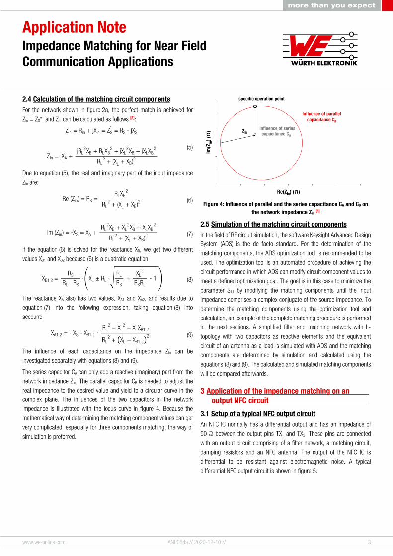
The series capacitor CA can only add a reactive (imaginary) part from the network impedance Zin. The parallel capacitor CB is needed to adjust the real impedance to the desired value and yield to a circular curve in the complex plane. The influences of the two capacitors in the network impedance is illustrated with the locus curve in figure 4. Because the mathematical way of determining the matching component values can get very complicated, especially for three components matching, the way of simulation is preferred.
Figure 4: Influence of parallel and the series capacitance CA and CB on
the network impedance Zin [5]
2.5 Simulation of the matching circuit components In the field of RF circuit simulation, the software Keysight Advanced Design System (ADS) is the de facto standard. For the determination of the matching components, the ADS optimization tool is recommended to be used. The optimization tool is an automated procedure of achieving the circuit performance in which ADS can modify circuit component values to meet a defined optimization goal. The goal is in this case to minimize the parameter S11 by modifying the matching components until the input impedance comprises a complex conjugate of the source impedance. To determine the matching components using the optimization tool and calculation, an example of the complete matching procedure is performed in the next sections. A simplified filter and matching network with L-topology with two capacitors as reactive elements and the equivalent circuit of an antenna as a load is simulated with ADS and the matching components are determined by simulation and calculated using the equations (8) and (9). The calculated and simulated matching components will be compared afterwards.
3 Application of the impedance matching on an output NFC circuit
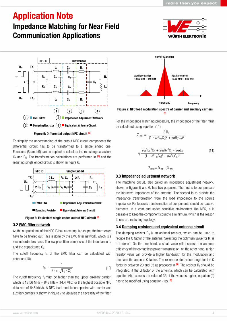
3.1 Setup of a typical NFC output circuit An NFC IC normally has a differential output and has an impedance of 50 Ω between the output pins TX1 and TX2. These pins are connected with an output circuit comprising of a filter network, a matching circuit, damping resistors and an NFC antenna. The output of the NFC IC is differential to be resistant against electromagnetic noise. A typical differential NFC output circuit is shown in figure 5.
www.we-online.com ANP084a // 2020-12-10 // 4
Impedance Matching for Near Field Communication Applications
Application Note
Figure 5: Differential output NFC circuit [5]
To simplify the understanding of the output NFC circuit components the differential circuit has to be transformed to a single ended one. Equations (8) and (9) can be applied to calculate the matching capacitors CA and CB. The transformation calculations are performed in [6] and the resulting single ended circuit is shown in figure 6.
Figure 6: Equivalent single ended output NFC circuit [5]
3.2 EMC filter network As the output signal of the NFC IC has a rectangular shape, the harmonics have to be filtered out. This is done by the EMC filter network, which is a second order low pass. The low pass filter comprises of the inductance L0 and the capacitance C0.
The cutoff frequency fC of the EMC filter can be calculated with equation (10).
fC = 1
2 ⋅ π L0 ⋅ C0 (10)
The cutoff frequency fC must be higher than the upper auxiliary carrier, which is 13.56 MHz + 848 kHz = 14.4 MHz for the highest possible NFC data rate of 848 kbit/s. A NFC load modulation spectra with carrier and auxiliary carriers is shown in figure 7 to visualize the necessity of the filter.
Figure 7: NFC load modulation spectra of carrier and auxiliary carriers
[7]
For the impedance matching procedure, the impedance of the filter must be calculated using equation (11).
ZEMC = 2 RD
(1 - ω2L0C0)² + (ωRDC0)²
-j 2ω3L0
2C0 + 2ωRD2C0 - 2ωL0
(1 - ω2L0C0)² + (ωRDC0)²
ZEMC= REMC -jXEMC
(11)
3.3 Impedance adjustment network The matching circuit, also called an impedance adjustment network, shown in figures 5 and 6, has two purposes. The first is to compensate the inductive impedance of the antenna. The second is to provide the impedance transformation from the load impedance to the source impedance. For lossless transformation all components should be reactive elements. In a cost and space sensitive environment like NFC, it is desirable to keep the component count to a minimum, which is the reason to use a L matching topology.
3.4 Damping resistors and equivalent antenna circuit The damping resistor Rq is an optional resistor, which can be used to reduce the Q factor of the antenna. Selecting the optimum value for Rq is a trade-off. On the one hand, a small value will increase the antenna efficiency of the contactless power transmission, on the other hand, a high resistor value will provide a higher bandwidth for the modulation and decrease the antenna Q factor. The recommended value range for the Q factor is between 20 and 35 as proposed in [8]. The resistor Rq should be integrated, if the Q factor of the antenna, which can be calculated with equation (4), exceeds the value of 35. If the value is higher, equation (4) has to be modified using equation (12). [5]
www.we-online.com ANP084a // 2020-12-10 // 5
Impedance Matching for Near Field Communication Applications
Application Note
QL,mod = Im(ZL,mod) Re(ZL,mod)
= XL
2 Rq + RL (12)
This leads to the following formula to calculate the damping resistor value Rq (for QL,mod ≥ 35):
Rq = 0.5XL
QL,mod - RL (13)
The last part of the output network is the equivalent antenna network, which is described in section 2.2. This network has been utilized for the simulations and calculations of the load impedance.
3.5 Six Steps to match an NFC IC to a WE NFC antenna As an example, it is described step by step how the NFC antenna of 760308101312 (see figure 8) can be matched to any arbitrary NFC IC with a differential output impedance of 50 Ω by calculation and simulation. The differential output circuit, shown in figure 5, has been used in the example.
Figure 8: WE WPT/NFC combination transmitter coil 760308101312
The following steps have to be performed, to implement the impedance matching by calculation and simulation:
1. Measure the series equivalent resistance Ra and the inductance La at the operating frequency fop = 13.56 MHz and the self resonance frequency fS of the coil 760308101312 with an network analyzer. Calculation of the parallel capacitance Ca with equation (2) and determination of the equivalent antenna circuit (see figure 3).
2. The resulting values of Ra, La and Ca have to be inserted into equation (3). The load impedance ZL with real part RL and imaginary part XL has to be calculated. The Q factor has to be calculated with equation (4).
3. The capacitance C0 and the inductance L0 of the EMC filter network must be determined with equation (10) and inserted into equation (11), so that the complex impedance ZEMC with real part REMC and imaginary part XEMC can be calculated.
4. The values for RL, XL, REMC (denoted as RS in equations (8) and (9)) and XEMC (denoted as XS in equations (8) and (9)) have to be integrated into the in equations (8) and (9). The capacitor values CA and CB have to be calculated out of XA and XB.
5. Verification of the matching calculation results by determining |S11|.
6. Simulation of the S11 parameter of the differential output circuit (see figure 5) and comparison of the results with the calculation.
3.6 Determination of the equivalent antenna circuit For the NFC antenna of article 760308101312 the following parameters have been determined by measurement and calculation:
Parameter Value Unit Way of determination
fS 63 MHz Measurement with VNA
La 0.7 µH Measurement with VNA
Ra 1.7 Ω Measurement with VNA
Ca 9.12 pF Calculated with eq. 2
Table 2: Parameters of the equivalent antenna circuit of 760308101312
The values for La and Ra have been measured at 13.56 MHz.
The equivalent antenna circuit parameters of the articles 760308101150, 760308103305, 760308102306 and 760308103307 are listed in the appendix A.2.
3.7 Determination of the complex impedance and the Q factor
The complex impedance ZL of the NFC antenna of coil 760308101312 is calculated with equation (3) by integrating the parameters of the equivalent antenna circuit, which have been determined in the previous section and lead to the following complex impedance value.
ZL = (1.87 + j 62.53) Ω
This leads due to equation (4) to a QL of 33. Because the Q factor of the antenna is lower than 35, the damping resistors Rq can be omitted.
3.8 Calculation of the filter components and the complex impedance of the filter network
For the cut off frequency fC, which can be calculated with equation (10), a value of 14.8 MHz has been chosen, which is higher than 14.4 MHz. An inductor value of 470 nH is chosen for L0, which leads to a C0 of 247 pF. The values L0 and C0 have to be inserted into equation (11) to calculate the complex filter impedance. For RD, the value of 25 Ω is inserted, which is the differential output impedance of a typical NFC IC in relation to the ground signal. These values lead to the following complex filter impedance:
ZEMC = (165.82 – j 45.46) Ω
3.9 Calculation of the matching component values The matching reactances XB and XA can be directly calculated with equations (8) and (9). For RS, the real part of the EMC network has to be integrated, which is 165.82 Ω. For the imaginary part of the source XS the imaginary part of the EMC filter has to be integrated, which is -45.46 Ω.

www.we-online.com ANP084a // 2020-12-10 // 6
Impedance Matching for Near Field Communication Applications
Application Note
For RL and XL, the real and imaginary parts of the antenna network have to be integrated, which are 1.87 Ω and 62.53 Ω. The resulting matching reactances XA and XB can be calculated to the corresponding differential matching capacitors CA and CB with:
CA,B = - 2
ω⋅XA,B (14)
Table 3 gives an overview of the resulting reactance and capacitance values.
Parameter Value Unit From equation
XB1 -69.69 Ω (8)
XA1 -519.81 Ω (9)
XB2 -56.8 Ω (8)
XA2 610.73 Ω (9)
CB1 337 pF (14)
CA1 45 pF (14)
CB2 413 pF (14)
CA2 -38 pF (14)
Table 3: Resulting reactance and capacitor values
The capacitor values for CA1 and CB1 are used for the matching, the values for CA2 and CB2 are neglected, because CA2 yields a negative value. Therefore the resulting matching capacitors for the differential output circuit are:
CA = 45 pF
CB = 337 pF
3.10 Calculation of the resulting reflection coefficient To verify, if the calculated matching capacitor values CA and CB yield to a low reflection, the S11 parameter at the output of the NFC IC must be calculated. The smaller the absolute values is, the lower is the reflection and the better is the circuit matched to the 50 Ω output impedance of the NFC IC. The complex input port voltage reflection coefficient S11 can be calculated with formula (15).
S11= Zin
' - 2RD
Zin' + 2RD
(15)
where RD = 25 Ω, which is the single ended output impedance of the NFC IC. The parameter Zin’ depends on the input impedance Zin (see equation (5)) and can be calculated with equation (16).
Zin'=
2 ∙ Zin
2 + jωC0Zin + 2jωL0 (16)
The absolute value of S11 can be calculated as:
|S11| = Re(S11)² + Im (S11)² (17)
In RF engineering, |S11| is often given in a logarithmic scale, and can be calculated as:
|S11|dB = 20 ∙ log(|S11|) (18)
The resulting values of equations (5), (15)-(18) are shown in table 4.
Parameter Value Unit From equation
Zin 167.15 + j 45.69 Ω (5)
Zin’ 49.7 – j 0.276 Ω (16)
S11 -0.00297-j 0.00277 (15)
|S11| 0.004 (17)
|S11|dB -48 dB (18)
Table 4: Calculated values for the reflection coefficient and the input impedance
3.11 Simulation of the differential output circuit with Keysight ADS
An alternative and easier way to determine the matching capacitor values CA and CB is to simulate the differential output network shown in figure 5. The optimization tool, integrated in ADS, allows the determination of unknown parameters of the network. A simulation goal and the simulation parameters have to be defined. To determine the matching capacitor values by simulation, the following steps have to be performed:
1. Create the schematic of the differential output network shown in figure 5 with the filter component values calculated in section 3.8 and the equivalent antenna network values determined in section 3.6. An input port with a 50 Ω impedance has been used.
2. Definition of the simulation type and the simulation variables 3. Definition of the optimization goal and the optimization iterations 4. Execution of the optimization and definition of the output plot type
3.12 Schematic of the differential output network Figure 9 shows the ADS schematic of the differential output network (see figure 5) with input port 1 and source impedance of 50 Ω.
Figure 9: ADS schematic of the differential output network
www.we-online.com ANP084a // 2020-12-10 // 7
Impedance Matching for Near Field Communication Applications
Application Note
3.13 Definition of the simulation type and the simulation variables
The chosen simulation type is the Large-Signal S-Parameter Simulation, which is based on a harmonic balance algorithm. This simulation type computes S-parameters for linear and nonlinear RF circuits. The simulation variables are the matching capacitors CA and CB, which have to be determined by the algorithm. The range of 1-1000 pF has been chosen. For the two capacitors, start values have to be defined.
3.14 Definition of the optimization goal and iterations As an optimization goal, it has been defined that |S11| should be less than 0.0001 in a frequency band between 13.559 MHz and 13.561 MHz. 1000 optimzation iterations have been chosen.
3.15 Execution of the optimization and definition of the output plot type
The simulated matching capacitance values result to CA = 45 pF and CB = 337 pF, which are the same values calculated in section 3.9.
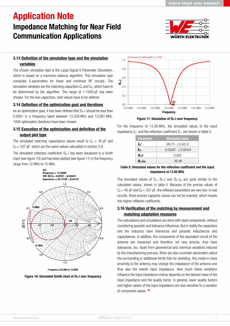
The simulated reflection coefficient |S11| has been visualized in a Smith chart (see figure 10) and has been plotted (see figure 11) in the frequency range from 12 MHz to 15 MHz.
Figure 10: Simulated Smith chart of |S11| over frequency
Figure 11: Simulation of |S11| over frequency
For the frequency of 13.56 MHz, the simulated values of the input impedance Zin’ and the reflection coefficient S11 are shown in table 5.
Parameter Simulated value
Zin’ (49.73 - j 0.42) Ω
S11 -0.00267 - j 0.00424
|S11| 0.005
|S11|dB -46 dB
Table 5: Simulated values for the reflection coefficient and the input impedance at 13.56 MHz
The simulated values of S11, |S11| and |S11|dB are quite similar to the calculated values, shown in table 4. Because of the precise values of CA = 45 pF and CB = 337 pF, the reflexion parameters are very low. In real circuits, these precise capacitor values can not be reached, which results into higher reflexion coefficents.
3.16 Verification of the matching by measurement and matching adaptation measures
The calculations and simulations are done with ideal components, without considering parasitic and tolerance influences. But in reality the capacitors and the inductors have tolerances and parasitic inductances and capacitances. In addition, the components of the equivalent circuit of the antenna are measured and therefore not very precise, thus have tolerances, too. Apart from geometrical and chemical variations induced by the manufacturing process, there are also uncertain parameters about the surrounding or additional ferrite foils for shielding. Any metal in close proximity to the antenna may change the impedance of the antenna and thus also the overall input impedance. How much these variations influence the input impedance mainly depends on the desired value of the input impedance and the quality factor. In general, lower quality factors and higher values of the input impedance are less sensitive to a variation of component values. [5]

www.we-online.com ANP084a // 2020-12-10 // 8
Impedance Matching for Near Field Communication Applications
Application Note
In view of these variations, an additional iteration of the matching is necessary. In the first step, the differential output circuit, which is shown in figure 5, with the calculated matching capacitor values has to be manufactured. The second step is to measure the input impedance with a network analyzer. The matching capacitors CA and CB have to be adjusted, so that the input impedance reaches the value of 50 Ω.
3.17 Differential NFC output circuit board and reflection coefficient measurement
To design the PCB of the differential output circuit, the program Altium Designer V.18.1.19 has been used. The Altium schematic of the differential NFC output circuit is shown in figure 12.
Figure 12: Altium schematic of the differential NFC output circuit
For the filter inductance L0 = 470 nH (see L01 and L02 at figure 12) the WE part 744762247GA has been used. The filter capacitance C0 = 247 pF comprises of two 100 pF parts of the WE Caps Series with part number 85012006038 (see C01, C02, C04 and C05 at figure 12) and the 47 pF capacitor with part number 885012006055 (see C03 and C06 at figure 12). The same capacitor has been used for CA (see CA2 and CA4 at figure 12). The capacitance CB = 337 pF comprises of a 330 pF capacitor with WE part number 885012006041 (see CB1 and CB4 at figure 12) and a 6.8 pF capacitor with WE part number 885012006050 (see CB2 and CB5 at figure 12). At the input port J1 of the network, the following impedance vs. frequency dependency has been measured with an Agilent Technologies E5061 network analyzer in the frequency band between 12 MHz and 15 MHz.
Figure 13: Measurement of the reflection coefficient in dependence of
the frequency shown in a Smith chart
A marker at the frequency of 13.56 MHz shows an input impedance of 22.4 Ω + j 27.7 Ω.
Due to equations (15) to (18) the calculated logarithmic absolute value of the input port voltage reflection coefficient |S11|dB yields to -5.94 dB.
The value has been verified by measuring the |S11|dB in dependence of the frequency. The measurement result is shown in figure 14.
Figure 14: Measurement of the logarithmic absolute value of the input
port voltage reflection coefficient in dependence of the frequency
The marker at the frequency of 13.56 MHz yields |S11|dB = -5.92 dB. To improve the matching, at least one of the matching capacitors has to be adapted.

www.we-online.com ANP084a // 2020-12-10 // 9
Impedance Matching for Near Field Communication Applications
Application Note
3.18 Determination of the necessary adaption of the matching capacitance values by simulation
To determine which of the matching capacitors has to be adapted, the influence of both capacitors CA and CB on |S11| and Zin’ is investigated by an ADS parameter sweep simulation.
Figure 15 shows the Smith chart of |S11| in dependence of CA and CB at the frequency of 13.56 MHz.
Figure 15: Simulation of |S11| in dependence of CA and CB shown in a
Smith chart
The parameter sweep of CB goes from 300 pF to 370 pF in 0.7 pF steps, which is a 10 % variation of the nominal value of 337 pF and the parameter sweep of CA goes from 23 pF (the left curve) to 70 pF (right curve) in 2.5 pF steps, which is a variation of 50 % of the nominal value of 47 pF. In figure 15, the marker ‘m3’ shows the desired 50 Ω matching point, which occurs at the curve for CA = 45.3 pF. The red line indicates the tolerance range of the values of capacitance CA and the blue line indicates the difference of the capacitance CB, which leads from the measured impedance (indicated by marker ‘m4’) to a matching value of about -26.6 dB. At the marker ‘m4’, the value for CB is 322 pF, which is about 15 pF smaller than the value of 337 pF, which is reached at the real axis of the Smith chart. This implies, that a capacitor of 15 pF has to be added to CB, to reach the desired matching point. At the matching test board (see schematic at figure 12) for CB3 and CB6, two 15 pF capacitors (one at CB3 and one for CB6) have been soldered in (WE number 885012006052). After the integration of the capacitors, the measurement,
which is shown in the figures 13 and 14 has been repeated. The results are shown in the figures 16 and 17. The measurement shows, that the parameter |S11|dB changed from -5.92 dB to the value of -26.1 dB at a frequency of 13.56 MHz due to the optimization of CB.
Figure 16: Measurement of the reflection coefficient with frequency
shown in a Smith chart after the matching capacitor CB has been adapted
Figure 17: Measurement of the logarithmic absolute value of the input
port voltage reflection coefficient with frequency

www.we-online.com ANP084a // 2020-12-10 // 10
Impedance Matching for Near Field Communication Applications
Application Note
3.19 Determination of the necessary adaption of the matching capacitance values by calculation
The change of CB and CA to reach the necessary 50 Ω matching impedance can also be done mathematically. To do so, the following calculation steps have to be performed:
1. Integrate the measured value for Zin’ (e. g. 22.4 Ω + j 27.7 Ω) into equation (16) and solve the equation for Zin:
Zin = 4jωL0 - 2Zin
'
jωC0Zin'- 2 + 2ω2C0L0
= RS - jXS
= (87.18 - j 70.95) Ω
(19)
2. Integrate the imaginary part (XS = 70.95 Ω) and real part (RS = 87.18 Ω) of Zin calculated with equation (19) into the equations (8) and (9) and calculate XA1,2 and XB1,2. XB1 = -73 Ω XB2 = -54.74 Ω XA1 = -489 Ω XA2 = 347.27 Ω 3. Use equation (14) to calculate the corresponding CA1,2 and CB1,2 values:
CB1 = 322 pF
CB2 = 429 pF
CA1 = 48 pF
CA2 = -67 pF
Because CA2 yields a negative value, the capacitances CB2 and CA2 can be neglected.
4. Determine the difference of the resulting CA and CB values to their calculated or simulated values. The calculated values (see section 3.9) for CA an CB are:
CA,calc = 45 pF
CB,calc = 337 pF
The values for CA and CB determined via measurement in the previous section are:
CA,meas = 48 pF
CB,meas = 322 pF
The differences of the capacitances ∆CA and ∆CB are:
∆CA = CA,calc - CA,meas - = 45 pF – 48 pF = -3 pF
∆CB = CB,calc - CB,meas = 337 pF - 322 pF = 15 pF
With these results, the capacitance CA has to be decreased by 3 pF and the capacitance CB has to be increased by 15 pF to reach a perfect impedance match. Because the difference value of ∆CA = 3 pF is about in the range of the tolerance of CA, this value has not been changed. In this section it has been shown by simulation and measurement, that the capacitance CB has to be increased by 15 pF to reach a matching value
of about -26 dB. It has to be considered, that the output circuit is differential, which means that the 15 pF has to be soldered twice into the matching circuit, at the places CB3 and CB6 (see figure 12).
4 Summary
This application note describes how a WE NFC antenna can be matched to a NFC IC. The determination of the matching capacitor values has been described by calculation and simulation. The measurement and necessary adaption of the input impedance to the source impedance has been shown. The basics of the complex impedance matching theory have been stated and typical L-matching topologies are shown. The calculation of the matching reactances and the determination of the Q factor have been performed. The different parts of differential output network have been analyzed and the dimensioning of the single components of the filter and the equivalent antenna components has been performed. Finally, the differential output network has been manufactured and the matching capacitors have been adapted to improve the matching.

www.we-online.com ANP084a // 2020-12-10 // 11
Impedance Matching for Near Field Communication Applications
Application Note
A Appendix
A.1 Bill of Materials
Index Description Size Specifications
fWPT = 125 kHz; fNFC = 13.56 MHz Partnumber
WPT/NFC
Combo Transmitter Coil Ø65 x 3.5 mm
L1,WPT = 6.3 µH, L2,NFC = 1.2 µH,
Q1,WPT = 100, Q2,NFC = 80 760308101150
WPT/NFC
Combo Transmitter Coil Ø54 x 4 mm
L1,WPT = 24 µH, L2,NFC = 0.7 µH,
Q1,WPT = 125, Q2,NFC = 30 760308101312
WPT/NFC
Combo Receiver Coil 45 x 44 x 0.72 mm
L1,WPT = 8.8 µH, L2,NFC = 1.6 µH
Q1,WPT = 30, Q2,NFC = 47 760308103305
WPT/NFC
Combo Receiver Coil 44 x 44 x 1 mm
L1,WPT = 8 µH, L2,NFC = 1.4 µH,
Q1,WPT = 19, Q2,NFC = 47 760308102306
WPT/NFC
Combo Receiver Coil 40 x 27 x 1 mm
L1,WPT = 7.8 µH, L2,NFC = 1.6 µH,
Q1,WPT = 19, Q2,NFC = 47 760308103307
L0 WE-KI
SMT Wire Wound Ceramic Inductor 1008 L = 470 nH, Q = 45 744762247GA
C0 WCAP-CSGP
Multilayer Ceramic Capacitor 0603 C = 100 pF 885012006038
C0 WCAP-CSGP
Multilayer Ceramic Capacitor 0603 C = 47 pF 885012006055
CA WCAP-CSGP
Multilayer Ceramic Capacitor 0603 CA1 = 47 pF 885012006055
CB1 WCAP-CSGP
Multilayer Ceramic Capacitor 0603 C = 330 pF 885012006052
CB2 WCAP-CSGP
Multilayer Ceramic Capacitor 0603 C = 6.8 pF 885012006041
CB3 WCAP-CSGP
Multilayer Ceramic Capacitor 0603 C = 15 pF 885012006050
J1 WR-SMA
SMA PCB THT Jack Straight SMA connector 60312002114503
J2 WR-TBL
Terminal Block 2.54 mm horizontal entry clamp 691210910002
A.2 Equivalent antenna circuit parameters
Artikelnummer fS (MHz) Ra (Ω) La (µH) Ca (pF)
760308101150 48 1.19 1.16 9.48
760308103305 50 4 1.58 6.4
760308102306 50 2.4 1.6 6.3
760308103307 54 3.7 1.7 5.1

www.we-online.com ANP084a // 2020-12-10 // 12
Impedance Matching for Near Field Communication Applications
Application Note
A.3 Literature
[1] C. Bowick, RF Circuit Design, 2nd Revised edition, Newnes, 2007, Pg 67. [2] K. Cartwright, Non-Calculus Derivation of the Maximum Power Transfer Theorem, Technology Interface, 8 (2), 2008. [3] M. Roland, Automatic Impedance Matching for 13.56 MHz NFC Antennas, 6th International Symposium on Communication Systems, Networks and Digital
Signal Processing, 2008. [4] Würth Elektronik eiSos, ANP057a, WE-MCA Multilayer Chip Antenna Placement & Matching, Application Note, 2018. [5] T. Baier: Automated Impedance Adjustment of 13.56 MHz NFC Reader Antennas, Master Thesis, 2014. [6] A. Schober, M. Ciacci, and M. Gebhart, An NFC Air Interface coupling model for Contactless System Performance estimation, International Conference on Telecommunications (ConTEL), June 2013. [7] Rohde und Schwarz, Near Field Communication (NFC) Technology and Measurements, White Paper, 2011. [8] NXP Corporation, AN11564, Antenna Design and Matching Guide, Application Note, 2016.

www.we-online.com ANP084a // 2020-12-10 // 13
Impedance Matching for Near Field Communication Applications
Application Note
I M P O R T A N T N O T I C E
The Application Note is based on our knowledge and experience of typical requirements concerning these areas. It serves as general guidance and should not be construed as a commitment for the suitability for customer applications by Würth Elektronik eiSos GmbH & Co. KG. The information in the Application Note is subject to change without notice. This document and parts thereof must not be reproduced or copied without written permission, and contents thereof must not be imparted to a third party nor be used for any unauthorized purpose. Würth Elektronik eiSos GmbH & Co. KG and its subsidiaries and affiliates (WE) are not liable for application assistance of any kind. Customers may use WE’s assistance and product recommendations for their applications and design. The responsibility for the applicability and use of WE Products in a particular customer design is always solely within the authority of the customer. Due to this fact it is up to the customer to evaluate and investigate, where appropriate, and decide whether the device with the specific product characteristics described in the product specification is valid and suitable for the respective customer application or not. The technical specifications are stated in the current data sheet of the products. Therefore the customers shall use the data sheets and are cautioned to verify that data sheets are current. The current data sheets can be downloaded at www.we-online.com. Customers shall strictly observe any product-specific notes, cautions and warnings. WE reserves the right to make corrections, modifications, enhancements, improvements, and other changes to its products and services. WE DOES NOT WARRANT OR REPRESENT THAT ANY LICENSE, EITHER EXPRESS OR IMPLIED, IS GRANTED UNDER ANY PATENT RIGHT,
COPYRIGHT, MASK WORK RIGHT, OR OTHER INTELLECTUAL PROPERTY RIGHT RELATING TO ANY COMBINATION, MACHINE, OR PROCESS IN WHICH WE PRODUCTS OR SERVICES ARE USED. INFORMATION PUBLISHED BY WE REGARDING THIRD-PARTY PRODUCTS OR SERVICES DOES NOT CONSTITUTE A LICENSE FROM WE TO USE SUCH PRODUCTS OR SERVICES OR A WARRANTY OR ENDORSEMENT THEREOF. WE products are not authorized for use in safety-critical applications, or where a failure of the product is reasonably expected to cause severe personal injury or death. Moreover, WE products are neither designed nor intended for use in areas such as military, aerospace, aviation, nuclear control, submarine, transportation (automotive control, train control, ship control), transportation signal, disaster prevention, medical, public information network etc. Customers shall inform WE about the intent of such usage before design-in stage. In certain customer applications requiring a very high level of safety and in which the malfunction or failure of an electronic component could endanger human life or health, customers must ensure that they have all necessary expertise in the safety and regulatory ramifications of their applications. Customers acknowledge and agree that they are solely responsible for all legal, regulatory and safety-related requirements concerning their products and any use of WE products in such safety-critical applications, notwithstanding any applications-related information or support that may be provided by WE. CUSTOMERS SHALL INDEMNIFY WE AGAINST ANY DAMAGES ARISING OUT OF THE USE OF WE PRODUCTS IN SUCH SAFETY-CRITICAL APPLICATIONS.
U S E F U L L I N K S
Application Notes www.we-online.com/app-notes
REDEXPERT Design Plattform www.we-online.com/redexpert
Toolbox www.we-online.com/toolbox
Product Catalog www.we-online.com/products
C O N T A C T I N F O R M A T I O N
[email protected] Tel. +49 7942 945 - 0
Würth Elektronik eiSos GmbH & Co. KG Max-Eyth-Str. 1 ⋅ 74638 Waldenburg ⋅ Germany
www.we-online.com