Embed Size (px)
DESCRIPTION
Impedance matching
Citation preview
AdvancedImpedance Matching
Microwave Engineering
EE 172Dr. Ray Kwok

Advanced Impedance Matching - Dr. Ray Kwok
Advanced Impedance MatchingSo far….
• 2-elements tuning• Lumped Elements (L,C)
• Transmission Lines
• Stubs (single & double)• 1-port network
• single frequency
Now:
• are all tuning the same?
• wideband matching – multiple sections• multi-ports (simultaneously tuned)
Advanced Impedance Matching - Dr. Ray Kwok
Let’s compare our 2-element tuning examples over frequency…
• Lumped Elements (L,C)
• Transmission Lines
• Stubs (Single and Double)• Quarter-Wave transformer

Advanced Impedance Matching - Dr. Ray Kwok
LumpedElements
R=1G=1
If ZL is inside the G=1 circle,
first element cannot be shunt
ZL (0.4, 1)YL (0.34, -0.87)
Z (0.4, 0.48)Y (1, -1.24)
=0.4+j1ZL
jB = +j1.24 = jZoωC
jX = -j0.52 = -j/ωCZo
Z (0.4, -0.48)Y (1, 1.24)
=0.4+j1ZL
jB = -j1.24 = -jZo/ωL
jX = -j1.48 = -j/ωCZo
Z (1, 1.4)Y (0.34, -0.48)
jB = +j0.39 = jZoωC
=0.4+j1ZL
jX = -j1.4 = -j/ωCZo
Z (1, -1.4)Y (0.34, 0.48)
jB = +j1.35 = jZoωC
=0.4+j1ZL
jX = j1.4 = jωL/Zo
If ZL is inside the R=1 circle,
first element cannot be in series

Advanced Impedance Matching - Dr. Ray Kwok
Return Loss
0.01 0.11 0.21 0.31 0.41 0.5
Frequency (GHz)
Lump
-50
-40
-30
-20
-10
0
DB(|S[1,1]|)
Lump1
DB(|S[1,1]|)
Lump2
DB(|S[1,1]|)
Lump3
DB(|S[1,1]|)
Lump4

Advanced Impedance Matching - Dr. Ray Kwok
Using Stubs
ZL (0.4, 1)YL (0.34, -0.87)
Z (0.4, -0.48)Y (1, 1.24)
=0.4+j1ZL
short shunt stub
jB = -j1.24 = -jcotβl
open series stub
jX = -j1.48 = -jcotβl
Z (1, 1.4)Y (0.34, -0.48)
open shunt stub
jB = +j0.39 = jtanβl
=0.4+j1ZL
open series stub
jX = -j1.4 = -jcotβl
l
l
l
l
β=
β−=
β−=
β=
tanjYY
cotjYY
cotjZZ
tanjZZ
oop
osh
oop
osh
One way, simply replace lumped elements with stubs
Zo can be
anything here
previous example

Advanced Impedance Matching - Dr. Ray Kwok
Open – Short Stubs
0.01 0.11 0.21 0.31 0.41 0.5
Frequency (GHz)
Stubs
-50
-40
-30
-20
-10
0
DB(|S[1,1]|)
Stub1
DB(|S[1,1]|)
Stub2

Advanced Impedance Matching - Dr. Ray Kwok
ZL (0.4, 1)YL (0.34, -0.87)
=0.4+j1ZL
Transmission Line Matching
usually requires 1 more element
previous example
0.130λλλλ
0.185λλλλ
0.055λ
50 Ω
jX = -j1.85 = -j/ωCZo
=0.4+j1ZL
0.435λλλλ
0.305λ
50 Ω
Y (1, 1.9)
short shunt stub
jB = -j1.9 = -jcotβl
Z (1, 1.85)

Advanced Impedance Matching - Dr. Ray Kwok
Single Stub Tuningrefers to sliding a stub (any kind)
along a transmission line.
previous example
0.130λλλλ
0.064λλλλ
=0.4+j1ZL
0.435λλλλ
0.305λ
50 Ω
Y (1, 1.9)
short shunt stub
jB = -j1.9 = -jcotβl
In practice, usually shunt stubs,
short stub for waveguides,
open stub for microstrip.
=0.4+j1ZL
0.434λ
50 Ω
open shunt stub
jB = j1.9 = jtanβl
ZL (0.4, 1)YL (0.34, -0.87)
Y (1, -1.9)
Advanced Impedance Matching - Dr. Ray Kwok
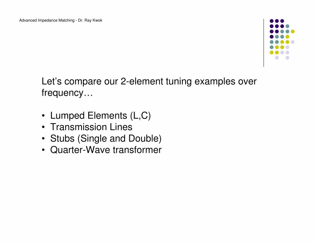
Any Stubtanβl can be “+” or “-”
previous example
0.130λλλλ
0.064λλλλ
=0.4+j1ZL
0.435λλλλ
0.305λ
50 Ω
Y (1, 1.9)
open shunt stub
jB = - j1.9 = jtanβlβl = -1.086 + π = 2.055length = 0.327λ > λ/4
can use any type depends on realization.
e.g. use shunt open stub only…
=0.4+j1ZL
0.434λ
50 Ω
open shunt stub
jB = j1.9 = jtanβlβl = 1.086length = 0.173λ
ZL (0.4, 1)YL (0.34, -0.87)
Y (1, -1.9)

Advanced Impedance Matching - Dr. Ray Kwok
Transmission Line + Stub
0.01 0.11 0.21 0.31 0.41 0.5
Frequency (GHz)
xline_stub
-50
-40
-30
-20
-10
0
DB(|S[1,1]|)
single_stub1
DB(|S[1,1]|)single_stub2
DB(|S[1,1]|)
single_stub3
DB(|S[1,1]|)single_stub4
DB(|S[1,1]|)
single_stub5

Advanced Impedance Matching - Dr. Ray Kwok
Double Stub Tuninge.g. 2 shunt short stubs (50Ω)
separated by a 50Ω line of 0.2λ
0.3λλλλ
0.5λλλλ
– 0.2λλλλ
• rotate the 1-circle by line length
• adjust d1 along constant-G circle
• stop at the rotated blue-circle
• xline will bring it to the green circle
• adjust d2 along the green circle to Zo
• not for all ZL !! Forbidden zone.
d1d2
ZL
0.2λ
50 Ω =0.4+j1
ZL(0.4,1)
YL(0.34,-0.87)
Y (0.34,-0.2)
Y (1,1.22)
-cotβd1 = +0.67βd1 = -0.98 +π = 2.16
d1 = 0.344λ
-cotβd2 = −1.22βd2 = 0.687
d2 = 0.109λ
50 Ω50 Ω

Advanced Impedance Matching - Dr. Ray Kwok
e.g. Quarter-Wavee.g. shunt stub (100Ω) then λ/4
ZL = 20 + j 50 Ω
• move Z to the real axis
• normalized Zc = √Z = √3.1; Zc = 1.76
• Zc = 50(1.76) = 88 Ω
ZL(0.4,1)
YL(0.34, -0.87)
Z (3.1,0)
Y(0.34,0)
(1/100) tanβd= (0.87)(1/50)βd = 1.05
d = 0.167λ
d
ZL
λ/4
Zc =0.4+j150 Ω
100Ω

Advanced Impedance Matching - Dr. Ray Kwok
Double Stub / Quarter-wave
0.01 0.11 0.21 0.31 0.41 0.5
Frequency (GHz)
double_n_quarter
-30
-20
-10
0
DB(|S[1,1]|)
double_stub
DB(|S[1,1]|)
quarter_wave

Advanced Impedance Matching - Dr. Ray Kwok
Mixed matching samples
0.01 0.11 0.21 0.31 0.41 0.5
Frequency (G Hz)
Mixed
-40
-30
-20
-10
0
DB(|S[1,1]|)
double_s tub
DB(|S[1,1]|)
Lump1
DB(|S[1,1]|)
quarter_wave
DB(|S[1,1]|)
single_stub2
DB(|S[1,1]|)
Stub 1

Advanced Impedance Matching - Dr. Ray Kwok
2-port tuning
2 – port
network
MatchingNetwork ?
Especially useful for active component design : amplifier (transistor)or inserting devices into a system (such as SAW filter…)
for matched load
11in S=Γ

Advanced Impedance Matching - Dr. Ray Kwok
Unmatched load (from previous lecture)
2 – port
networkb1
b2
a1a2 = ΓLb2
ZL
This is what we measure.
How does that affect our matching process?L22
21L1211in
1
1
L22
121L121111
L22
1212
2L221212221212
2L121112121111
2
1
2221
1211
2
1
S1
SSS
a
b
S1
aSSaSb
S1
aSb
bSaSaSaSb
bSaSaSaSb
a
a
SS
SS
b
b
Γ−
Γ+=Γ≡
Γ−Γ+=
Γ−=⇒
Γ+=+=
Γ+=+=
=

Advanced Impedance Matching - Dr. Ray Kwok
To what we match? (from previous lecture)
( ) ( ) ( )22
g
2
g
2
g
2
g
g
2
g
ininlossLoad
gg
2
XR4
RV
2
1
X2R2
RV
2
1RI
2
1PP
+=
+=== −
( ) 2
g
2
go
o
2
g
o
2
total
g
oLineLoadXRZ
ZV
2
1Z
Z
V
2
1ZI
2
1PP
2
++====
Case 1: match ZL = Zo = real → ΓL = 0, VSWR = 1 on the line
Zin lZo ZL
Zg=Rg + jXgVg
Zin
Zg
Vg
Case 2: match Zin = Zg → Γin = 0, VSWR > 1
g
2
g
2
g
g
2
g
LoadR
V
8
1
R4
RV
2
1P ===
Case 3: match Zin = Z*g → Xin = -Xg
= max power available
conjugate matching
Ideally, match all Zo = Zg = ZL = real, then all 3 PLoad are the same = Pmax.

Advanced Impedance Matching - Dr. Ray Kwok
Conjugate Match
Zo
Output
matching
Input
matching
Device
to be
matched
Zo
Γin
Γout
ΓL
ΓS
L22
21L1211in
S1
SSS
Γ−
Γ+=Γ
S11
21S1222out
S1
SSS
Γ−
Γ+=Γ
*
inS Γ=Γwant *
outL Γ=Γand

Advanced Impedance Matching - Dr. Ray Kwok
Simultaneous Conjugate Match G. Gonzales: Microwave Transistor Amplifiers
21122211
*
11222
*
22111
22
11
2
222
22
22
2
111
2
2
2
2
22
L
1
2
1
2
11
S
SSSSS
SSC
SSC
SS1B
SS1B
C2
C4BB
C2
C4BB
−==∆
∆−=
∆−=
∆−−+=
∆−−+=
−±=Γ
−±=Γ

Advanced Impedance Matching - Dr. Ray Kwok
Example
0 1.0
1.0
-1.0
10.0
10.0
-10.0
5.0
5.0
-5.0
2.0
2.0
-2.0
3.0
3.0
-3.0
4.0
4.0
-4.0
0.2
0.2
-0.2
0.4
0.4
-0.4
0.6
0.6
-0.6
0.8
0.8
-0.8
S_ParametersSwp Max
6GHz
Swp Min
6GHz
S[1,1]
ex1_raw_spara
S[2,2]
ex1_raw_spara
Match this FET at 6 GHz
o
2
2
2
2
22
L
o
1
2
1
2
11
S
o*
11222
o*
22111
22
11
2
222
22
22
2
111
o
21122211
9.103718.0C2
C4BB
3.177762.0C2
C4BB
9.1033911.0SSC
3.1774786.0SSC
8255.0SS1B
9928.0SS1B
1103015.0SSSSS
∠=−−
=Γ
∠=−−
=Γ
−∠=∆−=
−∠=∆−=
=∆−−+=
=∆−−+=
∠=−==∆
( )
−∠∠
∠−∠=
oo
oo
7.95572.05.28058.2
3.16057.03.171641.0S
Non-reciprocal, non-symmetrical
0 1.0
1.0
-1.0
10.0
10.0
-10.0
5.0
5.0
-5.0
2.0
2.0
-2.0
3.0
3.0
-3.0
4.0
4.0
-4.0
0.2
0.2
-0.2
0.4
0.4
-0.4
0.6
0.6
-0.6
0.8
0.8
-0.8
simulate_conjugateSwp Max
6GHz
Swp Min
6GHz
S[1,1]
ex1_conjugate_s11
S[1,1]
ex1_conjugate_s22
ΓS & ΓL
S11 & S22
Advanced Impedance Matching - Dr. Ray Kwok
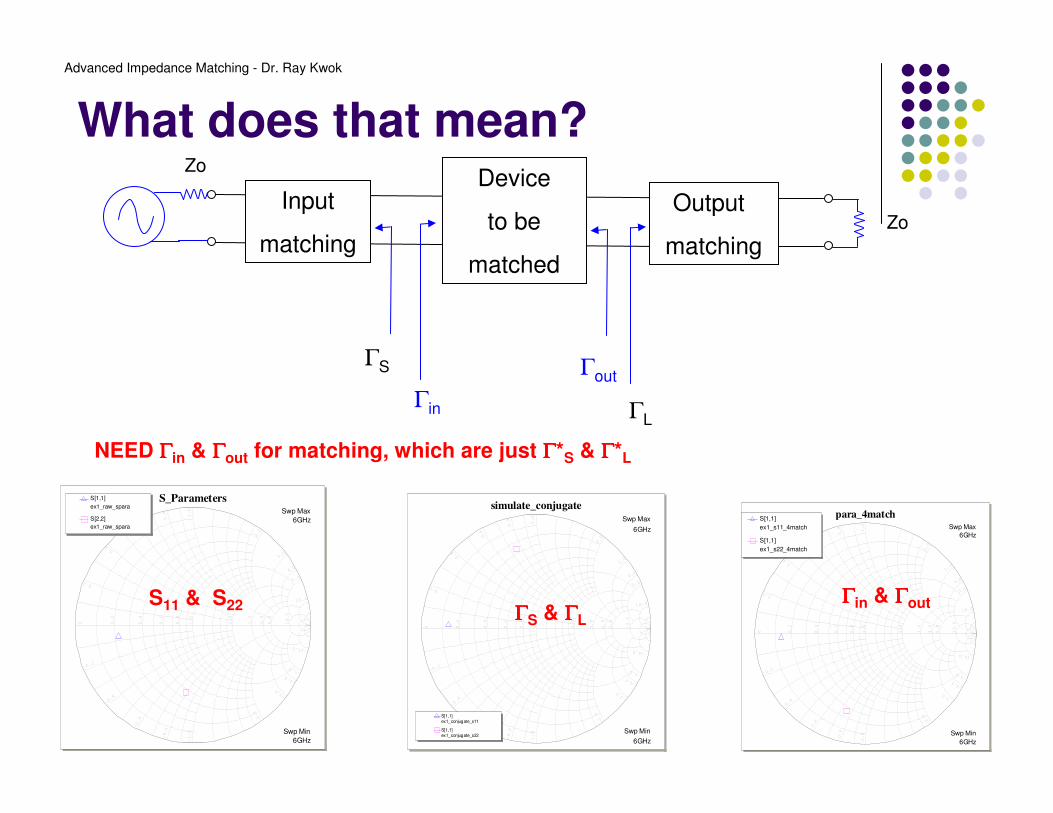
What does that mean?Zo
Output
matching
Input
matching
Device
to be
matched
Zo
Γin
Γout
ΓL
ΓS
NEED ΓΓΓΓin & ΓΓΓΓout for matching, which are just ΓΓΓΓ*S & ΓΓΓΓ*L
0 1.0
1.0
-1.0
10.0
10.0
-10.0
5.0
5.0
-5.0
2.0
2.0
-2.0
3.0
3.0
-3.0
4.0
4.0
-4.0
0.2
0.2
-0.2
0.4
0.4
-0.4
0.6
0.6
-0.6
0.8
0.8
-0.8
S_ParametersSwp Max
6GHz
Swp Min
6GHz
S[1,1]
ex1_raw_spara
S[2,2]
ex1_raw_spara
0 1.0
1.0
-1.0
10.0
10.0
-10.0
5.0
5.0
-5.0
2.0
2.0
-2.0
3.0
3.0
-3.0
4.0
4.0
-4.0
0.2
0.2
-0.2
0.4
0.4
-0.4
0.6
0.6
-0.6
0.8
0.8
-0.8
simulate_conjugateSwp Max
6GHz
Swp Min
6GHz
S[1,1]
ex1_conjugate_s11
S[1,1]
ex1_conjugate_s22
0 1.0
1.0
-1.0
10.0
10.0
-10.0
5.0
5.0
-5.0
2.0
2.0
-2.0
3.0
3.0
-3.0
4.0
4.0
-4.0
0.2
0.2
-0.2
0.4
0.4
-0.4
0.6
0.6
-0.6
0.8
0.8
-0.8
para_4matchSwp Max
6GHz
Swp Min
6GHz
S[1,1]
ex1_s11_4match
S[1,1]
ex1_s22_4match
S11 & S22ΓΓΓΓin & ΓΓΓΓout
ΓΓΓΓS & ΓΓΓΓL

Advanced Impedance Matching - Dr. Ray Kwok
Match 1-port at a timeIND
L=ID=
0.4827 nHL1
CAP
C=ID=
1.345 pFC1
1
SUBCKT
NET=ID=
"ex1_s11_4match" S2 PORT
Z=P=
50 Ohm1
CAP
C=ID=
0.899 pFC2
IND
L=ID=
1.572 nHL1
1
SUBCKT
NET=ID=
"ex1_s22_4match" S1
PORT
Z=P=
50 Ohm1
CAP
C=ID=
0.899 pFC2 CAP
C=ID=
1.345 pFC3
IND
L=ID=
0.4827 nHL1
IND
L=ID=
1.572 nHL2
1 2
SUBCKT
NET=ID=
"ex1_raw_spara" S1
PORT
Z=P=
50 Ohm1 PORT
Z=P=
50 Ohm2
Advanced Impedance Matching - Dr. Ray Kwok
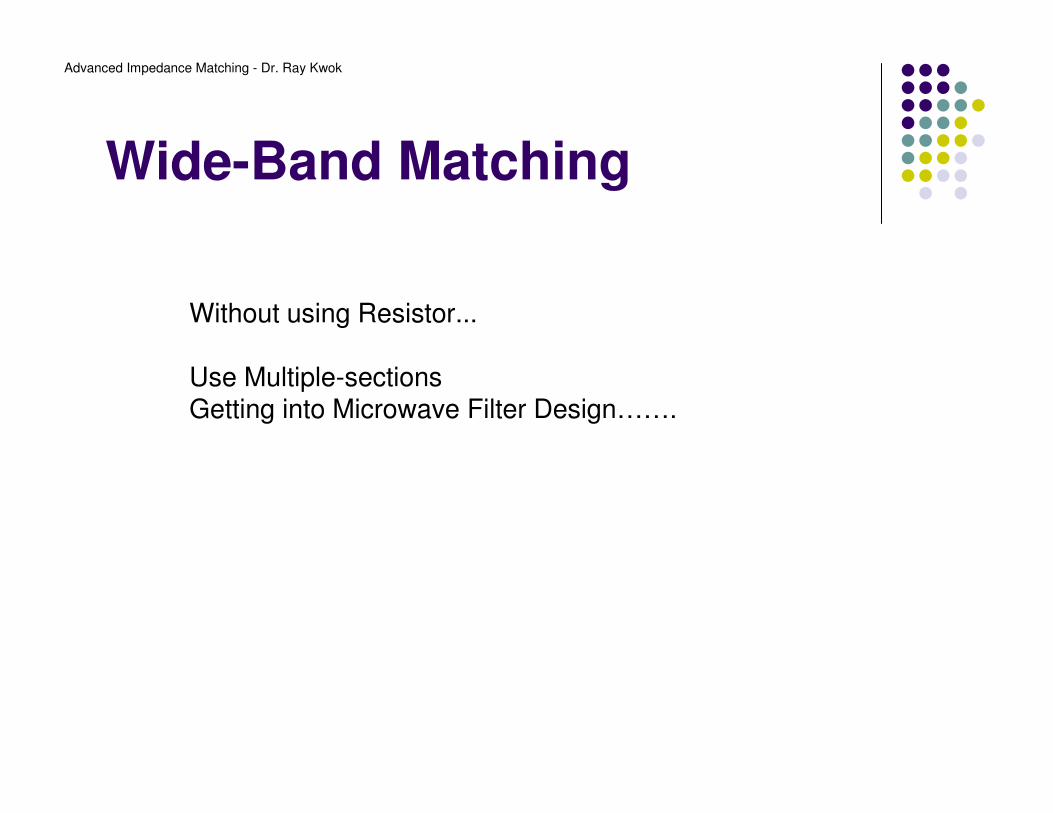
Wide-Band Matching
Without using Resistor...
Use Multiple-sectionsGetting into Microwave Filter Design…….
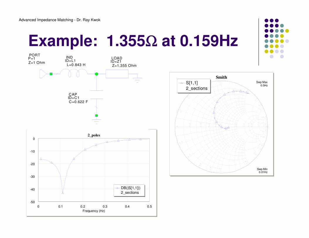
Advanced Impedance Matching - Dr. Ray Kwok
0 0.1 0.2 0.3 0.4 0.5
Frequency (Hz)
2_poles
-50
-40
-30
-20
-10
0
DB(|S[1,1]|)
2_sections
LOAD
Z=ID=
1.355 OhmZ1
CAP
C=ID=
0.622 FC1
IND
L=ID=
0.843 HL1
PORT
Z=P=
1 Ohm1
0 1.0
1.0
-1.0
10.0
10.0
-10.0
5.0
5.0
-5.0
2.0
2.0
-2.0
3.0
3.0
-3.0
4.0
4.0
-4.0
0.2
0.2
-0.2
0.4
0.4
-0.4
0.6
0.6
-0.6
0.8
0.8
-0.8
SmithSwp Max
0.5Hz
Swp Min0.01Hz
S[1,1]
2_sections
Example: 1.355ΩΩΩΩ at 0.159Hz
Advanced Impedance Matching - Dr. Ray Kwok
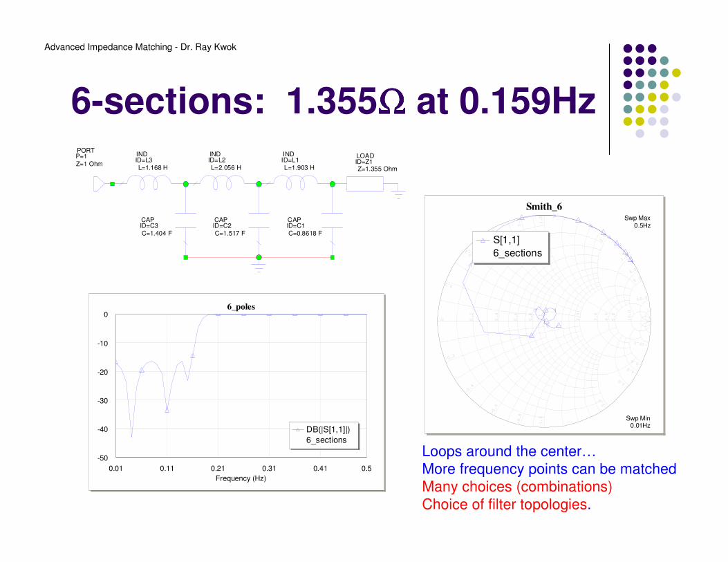
6-sections: 1.355ΩΩΩΩ at 0.159Hz
CAP
C=ID=
0.8618 FC1
IND
L=ID=
1.903 HL1
LOAD
Z=ID=
1.355 OhmZ1
CAP
C=ID=
1.517 FC2
IND
L=ID=
2.056 HL2
CAP
C=ID=
1.404 FC3
IND
L=ID=
1.168 HL3
PORT
Z=P=
1 Ohm1
0 1.0
1.0
-1.0
10.0
10.0
-10.0
5.0
5.0
-5.0
2.0
2.0
-2.0
3.0
3.0
-3.0
4.0
4.0
-4.0
0.2
0.2
-0.2
0.4
0.4
-0.4
0.6
0.6
-0.6
0.8
0.8
-0.8
Smith_6Swp Max
0.5Hz
Swp Min0.01Hz
S[1,1]
6_sections
0.01 0.11 0.21 0.31 0.41 0.5
Frequency (Hz)
6_poles
-50
-40
-30
-20
-10
0
DB(|S[1,1]|)
6_sections
Loops around the center…
More frequency points can be matched
Many choices (combinations)
Choice of filter topologies.

Advanced Impedance Matching - Dr. Ray Kwok
Example: 1:2 quarter-wave
LOAD
Z=ID=
2 OhmZ1
TLIN
F0=EL=Z0=ID=
1 GHz90 Deg1.414 OhmTL1
PORT
Z=P=
1 Ohm1
1.0
1.0
-1.0
2.0
0.2
-0.2
0.4
-0.4
0.6
0.6
-0.6
0.8
0.8
-0.8
1.2
1.2
1.4
1.6
1.8
0.1
-0.1
0.3
-0.3
0.5
0.5
-0.5
0.7
0.7
-0.7
0.9
0.9
-0.9
N1
Swp Max
2GHz
Swp Min
0.1GHz
S[1,1]
1_section
0.1 0.6 1.1 1.6 2
Frequency (GHz)
N1_RL
-60
-40
-20
0
DB(|S[1,1]|)
1_section

Advanced Impedance Matching - Dr. Ray Kwok
2-sections 1:2 quarter-waveTLIN
F0=EL=Z0=ID=
1 GHz90 Deg1.64 OhmTL1
LOAD
Z=ID=
2 OhmZ1
TLIN
F0=EL=Z0=ID=
1 GHz90 Deg1.219 OhmTL2
PORT
Z=P=
1 Ohm1
1.0
1.0
2.0
0.2
-0.2
0.4
-0.4
0.6
0.6
-0.6
0.8
0.8
-0.8
1.2
1.2
1.4
1.6
1.8
0.1
-0.1
0.3
-0.3
0.5
0.5
-0.5
0.7
0.7
-0.7
0.9
0.9
-0.9
N2
Swp Max
2GHz
Swp Min
0.1GHz
S[1,1]
2_sections
0.1 0.6 1.1 1.6 2
Frequency (GHz)
N2_RL
-50
-40
-30
-20
-10
0
DB(|S[1,1]|)
2_sections
Again, many choices of
the intermediate Z’s
Advanced Impedance Matching - Dr. Ray Kwok
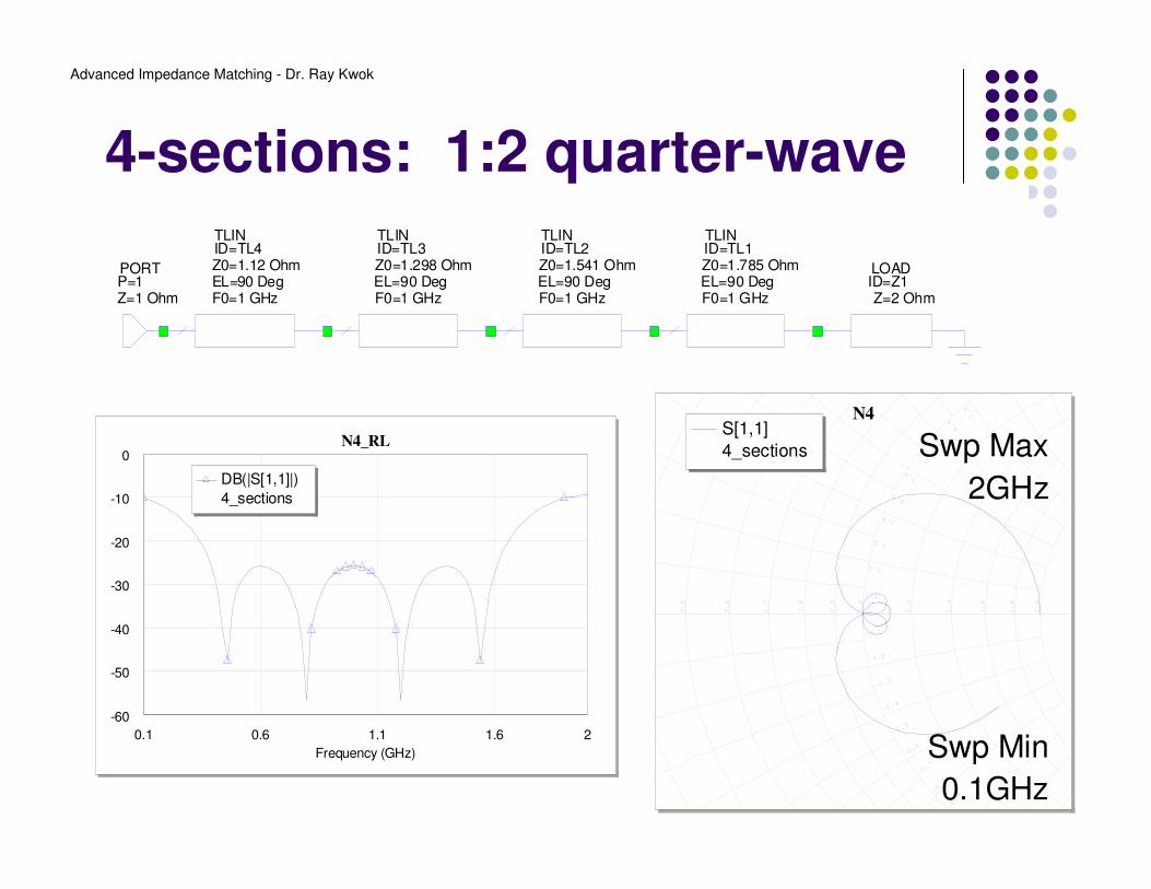
4-sections: 1:2 quarter-waveTLIN
F0=EL=Z0=ID=
1 GHz90 Deg1.785 OhmTL1
TLIN
F0=EL=Z0=ID=
1 GHz90 Deg1.541 OhmTL2
LOAD
Z=ID=
2 OhmZ1
TLIN
F0=EL=Z0=ID=
1 GHz90 Deg1.298 OhmTL3
TLIN
F0=EL=Z0=ID=
1 GHz90 Deg1.12 OhmTL4
PORT
Z=P=
1 Ohm1
1.0
1.0
2.0
0.2
-0.2
0.4
-0.4
0.6
0.6
-0.6
0.8
0.8
-0.8
1.2
1.2
1.4
1.6
1.8
0.1
-0.1
0.3
-0.3
0.5
0.5
-0.5
0.7
0.7
-0.7
0.9
0.9
-0.9
N4
Swp Max
2GHz
Swp Min
0.1GHz
S[1,1]
4_sections
0.1 0.6 1.1 1.6 2
Frequency (GHz)
N4_RL
-60
-50
-40
-30
-20
-10
0
DB(|S[1,1]|)
4_sections

Advanced Impedance Matching - Dr. Ray Kwok
Compare bandwidth
0.1 0.6 1.1 1.6 2
Frequency (GHz)
Return Loss
-60
-40
-20
0
DB(|S[1,1]|)
1_section
DB(|S[1,1]|)
2_sections
DB(|S[1,1]|)
4_sections
Advanced Impedance Matching - Dr. Ray Kwok
To be continued….
Choice of impedance of the intermediate
elements depends on the characteristic of the
performance desires (such as flat passband,
minimum phase variation, limited group delay
variation…etc)
It is a topic of future lectures.