Embed Size (px)
Citation preview

Impact of Cracking beneath Solder Pads in Printed Board Laminate on Reliability of Solder Joints to Ceramic Ball Grid Array Packages
ESA-STM-267
P.-E. Tegehall
IVF Industrial Research and Development Corporation, Sweden
B. D. Dunn
Materials and Processes Division
Directorate of Technology and Operational Support
European Space Agency
Abstract Thermal mismatch between ceramic ball grid array (CGBA) components and organic printed boards not only causes fatigue of the solder joints when exposed to thermal changes, but may also cause cracking of the printed board laminate beneath solder pads. Since cracks in the laminate reduce the stress on the solder joints caused by the thermal changes, they may actually improve the fatigue life of the solder joints. Even so, they may cause other failure mechanisms, and board laminate cracking must therefore be restricted. In this investigation, factors affecting board laminate cracking and its impact on the reliability of solder joints have been studied.
The results indicate that laminate cracking is common and difficult to avoid when large ceramic components are soldered to organic printed boards. Although not studied in this investigation, one of the main factors causing laminate cracking is probably the level of the low temperature extreme during thermal cycling. Stress relaxation and creep of solder cease at temperatures below about -20°C and the stress put on the laminate will therefore be higher the lower the low temperature extreme. In addition, the organic laminate will be more brittle the lower the temperature. Since laminate cracking may increase the fatigue life, this implies that performing thermal cycling down to -55°C may greatly overestimate the fatigue life in a more benign environment.
The temperature profile used during soldering was found to not significantly affect the extent of cracking of the printed board laminate when thermally cycled. In contrast, pad design had a large impact on laminate cracking. Cracking was completely eliminated if the pad was connected with a conductor on the inward side where cracking is initiated. Increasing the pad diameter also decreased the extent of cracking but not as efficiently as a conductor.
Although the soldering profile did not affect the extent of laminate cracking, it did impact the fatigue life of the solder joints. An increase of the peak temperature improved the fatigue life, probably due to increased melting temperature of the eutectic solder fillet between board pads and high-melt balls on the component. This is caused by dissolution of lead from the high-melt balls into the eutectic solder.
Optimisation of the geometry of the solder joint fillet between board pads and the high-melt balls is important for achieving long fatigue life. The fillet needs to have a convex surface with good wetting of solder pad edges for best result.
Exposure to vibration may cause laminate cracks already present to grow, resulting in improved fatigue life of the solder joints. In absence of cracks, vibration exposure may cause shortened fatigue life.
Uptake of humidity by the printed board prior to soldering seems to improve the fatigue life of the solder joints, although the results are inconclusive and the mechanism for the improvement has not been clarified.
Contents 1 INTRODUCTION 1
2 EXPERIMENTAL WORK 2
2.1 TEST MATRIX 2 2.2 CBGA PACKAGE 3 2.3 PRINTED BOARDS 4
3 SOLDERING OF TEST VEHICLES 8
3.1 BAKING OF PRINTED BOARDS 8 3.2 MOISTURE SOAKING OF PRINTED BOARDS 8 3.3 PRINTING OF SOLDER PASTE 8 3.4 SOLDERING OF PACKAGES 8 3.5 CLEANING 14
4 RELIABILITY ASSESSMENT METHODS 14
4.1 THERMAL-CYCLING TEST 14 4.2 VIBRATION TEST 15 4.3 ANALYSIS METHODS 16
5 RESULTS 16
5.1 IMPACT OF THERMAL CYCLING ON SOLDER JOINT RELIABILITY 17 5.2 DOGBONE DESIGN AND LOW PEAK TEMPERATURE 17 5.3 DOGBONE DESIGN AND HIGH PEAK TEMPERATURE, VAPOUR PHASE SOLDERING AND
MOISTURE SOAKING 24 5.4 VIA-IN-PAD DESIGN 30
6 DISCUSSION 38
6.1 FACTORS AFFECTING BOARD LAMINATE CRACKING 38 6.2 DISSOLUTION OF LEAD INTO EUTECTIC SOLDER 41 6.3 IMPACT ON RELIABILITY 42
7 CONCLUSIONS 42
8 ACKNOWLEDGEMENTS 43
9 REFERENCES 43
1
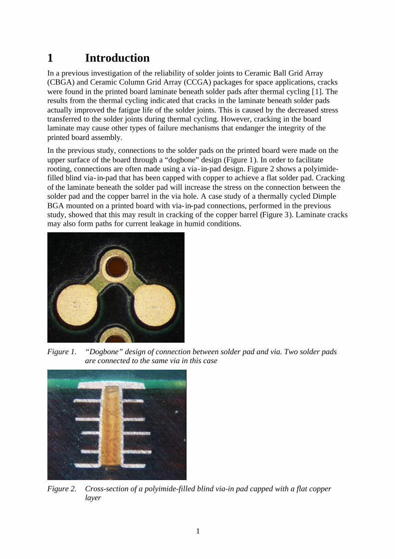
1 Introduction In a previous investigation of the reliability of solder joints to Ceramic Ball Grid Array (CBGA) and Ceramic Column Grid Array (CCGA) packages for space applications, cracks were found in the printed board laminate beneath solder pads after thermal cycling [1]. The results from the thermal cycling indicated that cracks in the laminate beneath solder pads actually improved the fatigue life of the solder joints. This is caused by the decreased stress transferred to the solder joints during thermal cycling. However, cracking in the board laminate may cause other types of failure mechanisms that endanger the integrity of the printed board assembly.
In the previous study, connections to the solder pads on the printed board were made on the upper surface of the board through a “dogbone” design (Figure 1). In order to facilitate rooting, connections are often made using a via- in-pad design. Figure 2 shows a polyimide-filled blind via- in-pad that has been capped with copper to achieve a flat solder pad. Cracking of the laminate beneath the solder pad will increase the stress on the connection between the solder pad and the copper barrel in the via hole. A case study of a thermally cycled Dimple BGA mounted on a printed board with via- in-pad connections, performed in the previous study, showed that this may result in cracking of the copper barrel (Figure 3). Laminate cracks may also form paths for current leakage in humid conditions.
Figure 1. “Dogbone” design of connection between solder pad and via. Two solder pads
are connected to the same via in this case
Figure 2. Cross-section of a polyimide-filled blind via-in pad capped with a flat copper
layer

2
Figure 3. Views showing the fracture between a pad and the board laminate for a corner
solder joint to a Dimple BGA analysed using a red dye penetrant. View (a) shows the solder ball with the underside of the ripped off pad and view (b) shows the location on the PCB where the ball was attached
There is not much written about laminate cracking beneath solder pads in the literature. According to IPC-7095, it is thought to be caused by thermal mechanical stress during reflow and/or subsequent mechanical stresses on the joints [2]. Besides mechanical stress, the susceptibility for cracking is likely influenced by the design, materials, and processes used for manufacturing the printed board assembly.
The aims of this study are to investigate to what extent the cracking is affected by the PCB design, how various factors during assembly affect the susceptibility for cracking, and which stresses precipitate the cracks.
2 Experimental Work
2.1 Test Matrix The experimental test matrix used in the investigation is presented in Table 1. Multilayer polyimide/glass PCBs with two different designs were used for the investigation, one with dogbone connections to the solder pads and one with via- in-pad connections. Two different PCB manufacturers produced the latter type of board.
The boards were mounted with ceramic BGAs. Various thermal profiles were used for soldering in order to evaluate how increased stress during soldering affected the cracking of the laminate. Also, the impact of humidity in the board laminate was investigated by moisture-soaking some of the boards prior to soldering.
After soldering, the test vehicles were thermally cycled between -55°C and +100°C for up to 1000 cycles. In order to assess the effect of vibration on the cracking mechanism some of the test vehicles were also exposed to a vibration test.

3
Table 1. Experiment test matrix used in the investigation
Board No.
Type of connection
Printed board manufacturer
Moisture-soak of printed board
Soldering profile Numb er of cycles
Exposure to vibration
A1 (Ref.) Dogbone X No Reflow, low peak 0 No A3 Dogbone X No Reflow, low peak 1000 Yes A4 Dogbone X No Reflow, low peak 500 Yes A5 Dogbone X No Reflow, low peak 1000 No A6 Dogbone X No Reflow, low peak 500 No A12 (Ref.) Dogbone X No Reflow, high peak 0 No A13 Dogbone X No Reflow, high peak 1000 No A14 Dogbone X No Reflow, high peak 500 No A15 (Ref.) Dogbone X No Vapour phase 0 No A16 Dogbone X No Vapour phase 500 No A17 Dogbone X No Vapour phase 1000 No A18 (Ref.) Dogbone X Yes Reflow, low peak 0 No A19 Dogbone X Yes Reflow, low peak 1000 No A20 Dogbone X Yes Reflow, low peak 500 No B2 (Ref.) Via-in-pad X No Reflow 0 No B3 Via-in-pad X No Reflow 500 Yes B4 Via-in-pad X No Reflow 1000 Yes B5 Via-in-pad X No Reflow 500 No B6 Via-in-pad X No Reflow 1000 No C1 (Ref.) Via-in-pad Y No Reflow 0 No C2 Via-in-pad Y No Reflow 500 Yes C3 Via-in-pad Y No Reflow 500 Yes C4 Via-in-pad Y No Reflow 500 No C5 Via-in-pad Y No Reflow 500 No
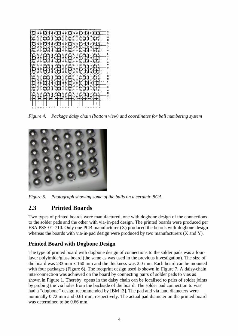
2.2 CBGA Package Ceramic ball grid array packages from IBM with a 2.0 mm thick ceramic multilayer substrate and an aluminium lid were used for the tests. They had 625 I/Os (25 x 25 full array) with a pitch of 1.27 mm and daisy-chain interconnection (Figure 4). The body size was 32.3 mm x 32.3 mm. No chip was mounted in the modules.
The balls consisted of high-melt solder (10% Sn/90% Pb) and the ball diameter was 0.89 mm. They were soldered to the modules using eutectic solder. A corner of a package is shown in Figure 5.
4
Figure 4. Package daisy chain (bottom view) and coordinates for ball numbering system
Figure 5. Photograph showing some of the balls on a ceramic BGA
2.3 Printed Boards Two types of printed boards were manufactured, one with dogbone design of the connections to the solder pads and the other with via- in-pad design. The printed boards were produced per ESA PSS-01-710. Only one PCB manufacturer (X) produced the boards with dogbone design whereas the boards with via-in-pad design were produced by two manufacturers (X and Y).
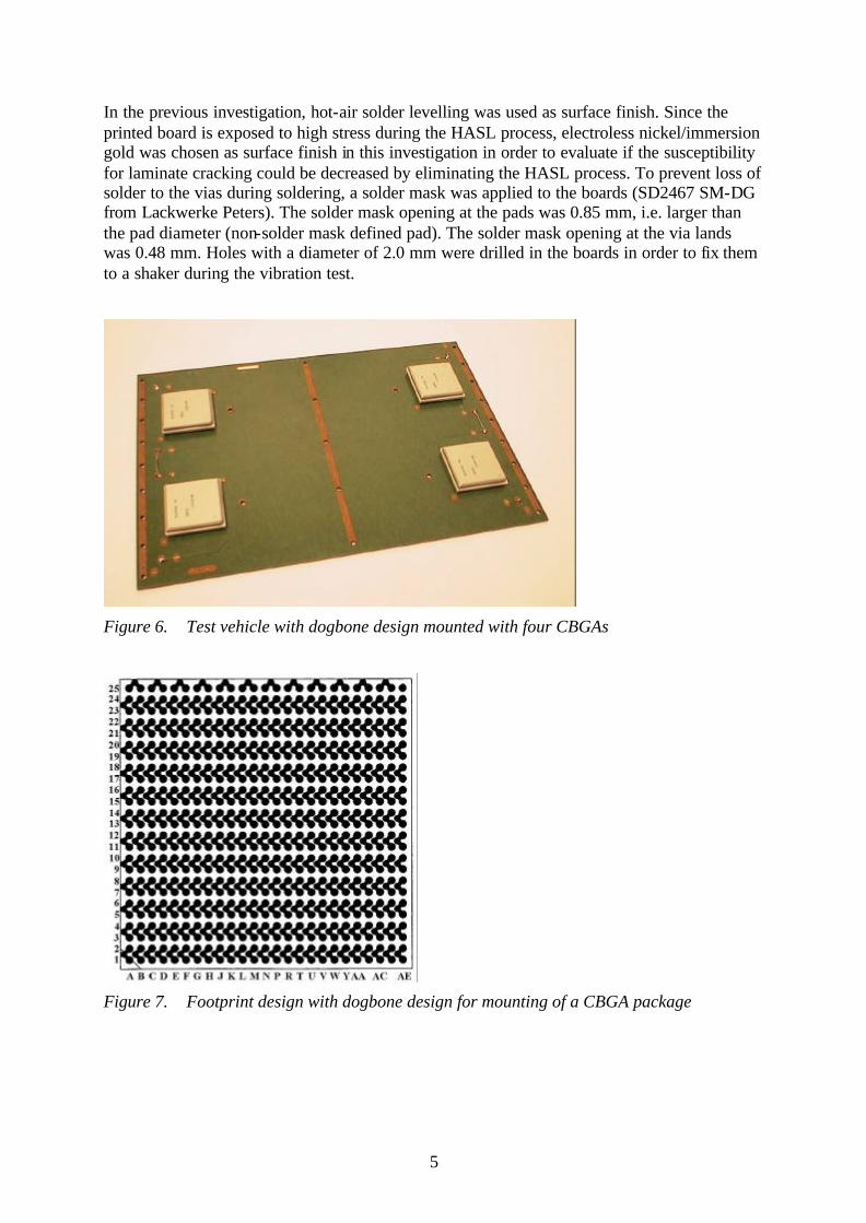
Printed Board with Dogbone Design The type of printed board with dogbone design of connections to the solder pads was a four-layer polyimide/glass board (the same as was used in the previous investigation). The size of the board was 233 mm x 160 mm and the thickness was 2.0 mm. Each board can be mounted with four packages (Figure 6). The footprint design used is shown in Figure 7. A daisy-chain interconnection was achieved on the board by connecting pairs of solder pads to vias as shown in Figure 1. Thereby, opens in the daisy chain can be localised to pairs of solder joints by probing the via holes from the backside of the board. The solder pad connection to vias had a “dogbone” design recommended by IBM [3]. The pad and via land diameters were nominally 0.72 mm and 0.61 mm, respectively. The actual pad diameter on the printed board was determined to be 0.66 mm.
5
In the previous investigation, hot-air solder levelling was used as surface finish. Since the printed board is exposed to high stress during the HASL process, electroless nickel/immersion gold was chosen as surface finish in this investigation in order to evaluate if the susceptibility for laminate cracking could be decreased by eliminating the HASL process. To prevent loss of solder to the vias during soldering, a solder mask was applied to the boards (SD2467 SM-DG from Lackwerke Peters). The solder mask opening at the pads was 0.85 mm, i.e. larger than the pad diameter (non-solder mask defined pad). The solder mask opening at the via lands was 0.48 mm. Holes with a diameter of 2.0 mm were drilled in the boards in order to fix them to a shaker during the vibration test.
Figure 6. Test vehicle with dogbone design mounted with four CBGAs
Figure 7. Footprint design with dogbone design for mounting of a CBGA package
6
Printed Board with Via-in-pad Design A twelve- layer polyimide/glass board was used for the via- in-pad design. The printed board had the same size as the board with dogbone design except that the nominal thickness was 2.2 mm. The vias in the pads consist of blind vias achieved through a sequential lamination technique. Two semi-finished boards with six layers and through holes are first created. These two semi-finished boards are pressed together with a pre-preg of glass- fibre weave and polyimide resin between. Polyimide resin from the pre-preg is then squeezed out in the via holes, completely filling them, and some surplus polyimide resin is pressed out through the holes. The surface is planarised and then capped with a flat copper layer that gives an appearance of a via- in-pad as shown in Figure 2.
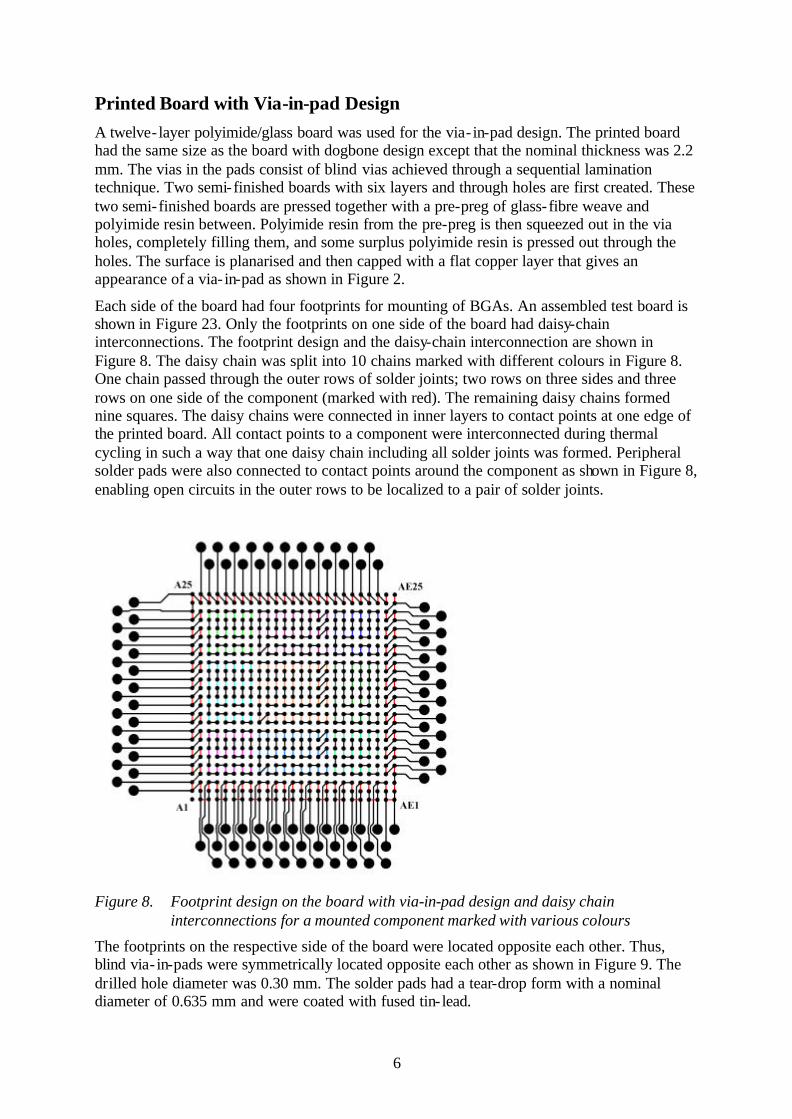
Each side of the board had four footprints for mounting of BGAs. An assembled test board is shown in Figure 23. Only the footprints on one side of the board had daisy-chain interconnections. The footprint design and the daisy-chain interconnection are shown in Figure 8. The daisy chain was split into 10 chains marked with different colours in Figure 8. One chain passed through the outer rows of solder joints; two rows on three sides and three rows on one side of the component (marked with red). The remaining daisy chains formed nine squares. The daisy chains were connected in inner layers to contact points at one edge of the printed board. All contact points to a component were interconnected during thermal cycling in such a way that one daisy chain including all solder joints was formed. Peripheral solder pads were also connected to contact points around the component as shown in Figure 8, enabling open circuits in the outer rows to be localized to a pair of solder joints.
Figure 8. Footprint design on the board with via-in-pad design and daisy chain
interconnections for a mounted component marked with various colours
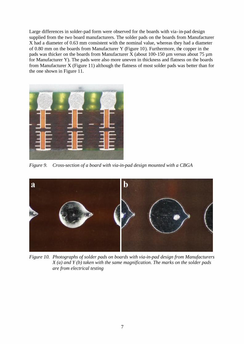
The footprints on the respective side of the board were located opposite each other. Thus, blind via- in-pads were symmetrically located opposite each other as shown in Figure 9. The drilled hole diameter was 0.30 mm. The solder pads had a tear-drop form with a nominal diameter of 0.635 mm and were coated with fused tin- lead.
7
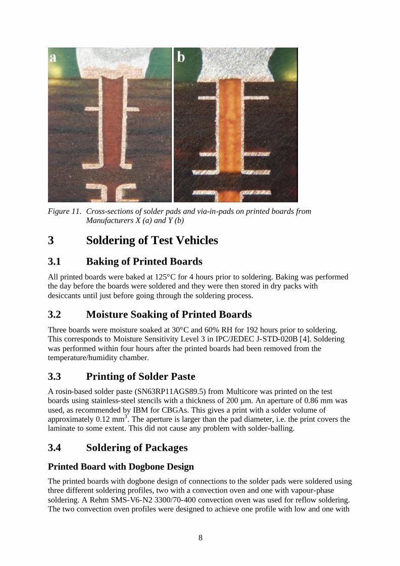
Large differences in solder-pad form were observed for the boards with via- in-pad design supplied from the two board manufacturers. The solder pads on the boards from Manufacturer X had a diameter of 0.63 mm consistent with the nominal value, whereas they had a diameter of 0.80 mm on the boards from Manufacturer Y (Figure 10). Furthermore, the copper in the pads was thicker on the boards from Manufacturer X (about 100-150 µm versus about 75 µm for Manufacturer Y). The pads were also more uneven in thickness and flatness on the boards from Manufacturer X (Figure 11) although the flatness of most solder pads was better than for the one shown in Figure 11.
Figure 9. Cross-section of a board with via-in-pad design mounted with a CBGA
Figure 10. Photographs of solder pads on boards with via-in-pad design from Manufacturers
X (a) and Y (b) taken with the same magnification. The marks on the solder pads are from electrical testing
8
Figure 11. Cross-sections of solder pads and via-in-pads on printed boards from
Manufacturers X (a) and Y (b)
3 Soldering of Test Vehicles
3.1 Baking of Printed Boards All printed boards were baked at 125°C for 4 hours prior to soldering. Baking was performed the day before the boards were soldered and they were then stored in dry packs with desiccants until just before going through the soldering process.
3.2 Moisture Soaking of Printed Boards Three boards were moisture soaked at 30°C and 60% RH for 192 hours prior to soldering. This corresponds to Moisture Sensitivity Level 3 in IPC/JEDEC J-STD-020B [4]. Soldering was performed within four hours after the printed boards had been removed from the temperature/humidity chamber.
3.3 Printing of Solder Paste A rosin-based solder paste (SN63RP11AGS89.5) from Multicore was printed on the test boards using stainless-steel stencils with a thickness of 200 µm. An aperture of 0.86 mm was used, as recommended by IBM for CBGAs. This gives a print with a solder volume of approximately 0.12 mm3. The aperture is larger than the pad diameter, i.e. the print covers the laminate to some extent. This did not cause any problem with solder-balling.
3.4 Soldering of Packages
Printed Board with Dogbone Design The printed boards with dogbone design of connections to the solder pads were soldered using three different soldering profiles, two with a convection oven and one with vapour-phase soldering. A Rehm SMS-V6-N2 3300/70-400 convection oven was used for reflow soldering. The two convection oven profiles were designed to achieve one profile with low and one with
9
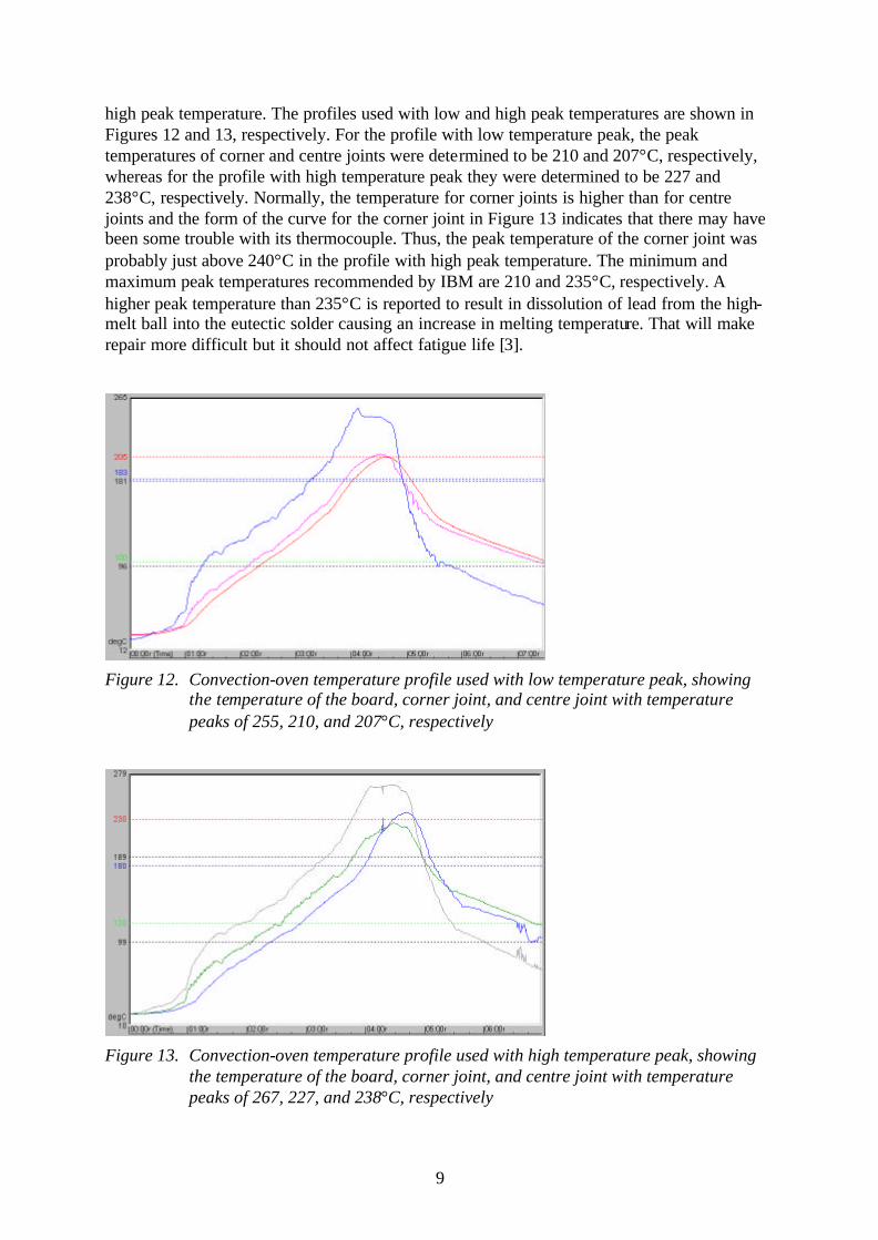
high peak temperature. The profiles used with low and high peak temperatures are shown in Figures 12 and 13, respectively. For the profile with low temperature peak, the peak temperatures of corner and centre joints were determined to be 210 and 207°C, respectively, whereas for the profile with high temperature peak they were determined to be 227 and 238°C, respectively. Normally, the temperature for corner joints is higher than for centre joints and the form of the curve for the corner joint in Figure 13 indicates that there may have been some trouble with its thermocouple. Thus, the peak temperature of the corner joint was probably just above 240°C in the profile with high peak temperature. The minimum and maximum peak temperatures recommended by IBM are 210 and 235°C, respectively. A higher peak temperature than 235°C is reported to result in dissolution of lead from the high-melt ball into the eutectic solder causing an increase in melting temperature. That will make repair more difficult but it should not affect fatigue life [3].
Figure 12. Convection-oven temperature profile used with low temperature peak, showing
the temperature of the board, corner joint, and centre joint with temperature peaks of 255, 210, and 207°C, respectively
Figure 13. Convection-oven temperature profile used with high temperature peak, showing
the temperature of the board, corner joint, and centre joint with temperature peaks of 267, 227, and 238°C, respectively
10
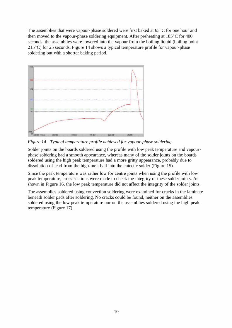
The assemblies that were vapour-phase soldered were first baked at 65°C for one hour and then moved to the vapour-phase soldering equipment. After preheating at 185°C for 400 seconds, the assemblies were lowered into the vapour from the boiling liquid (boiling point 215°C) for 25 seconds. Figure 14 shows a typical temperature profile for vapour-phase soldering but with a shorter baking period.
Figure 14. Typical temperature profile achieved for vapour-phase soldering
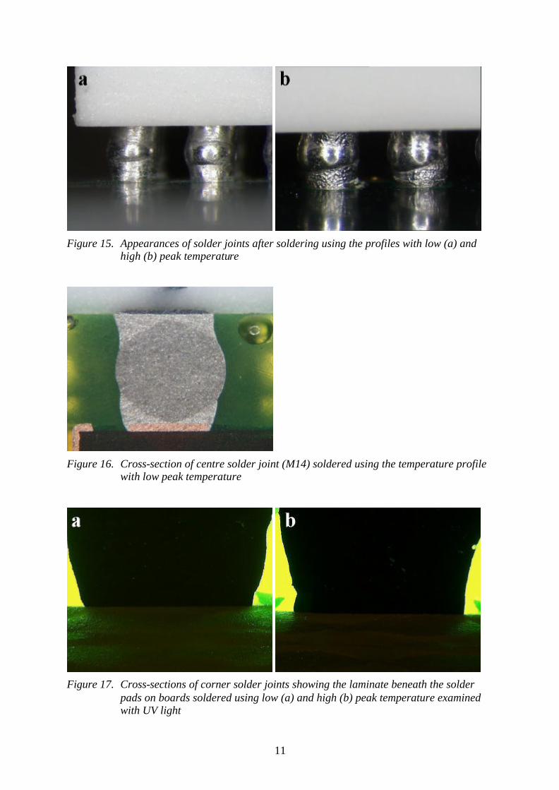
Solder joints on the boards soldered using the profile with low peak temperature and vapour-phase soldering had a smooth appearance, whereas many of the solder joints on the boards soldered using the high peak temperature had a more gritty appearance, probably due to dissolution of lead from the high-melt ball into the eutectic solder (Figure 15).
Since the peak temperature was rather low for centre joints when using the profile with low peak temperature, cross-sections were made to check the integrity of these solder joints. As shown in Figure 16, the low peak temperature did not affect the integrity of the solder joints.
The assemblies soldered using convection soldering were examined for cracks in the laminate beneath solder pads after soldering. No cracks could be found, neither on the assemblies soldered using the low peak temperature nor on the assemblies soldered using the high peak temperature (Figure 17).
11
Figure 15. Appearances of solder joints after soldering using the profiles with low (a) and
high (b) peak temperature
Figure 16. Cross-section of centre solder joint (M14) soldered using the temperature profile
with low peak temperature
Figure 17. Cross-sections of corner solder joints showing the laminate beneath the solder
pads on boards soldered using low (a) and high (b) peak temperature examined with UV light
12
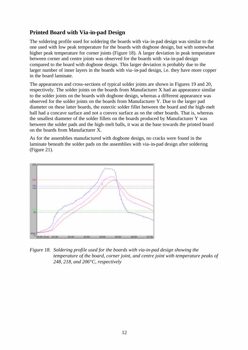
Printed Board with Via-in-pad Design The soldering profile used for soldering the boards with via- in-pad design was similar to the one used with low peak temperature for the boards with dogbone design, but with somewhat higher peak temperature for corner joints (Figure 18). A larger deviation in peak temperature between corner and centre joints was observed for the boards with via-in-pad design compared to the board with dogbone design. This larger deviation is probably due to the larger number of inner layers in the boards with via- in-pad design, i.e. they have more copper in the board laminate.
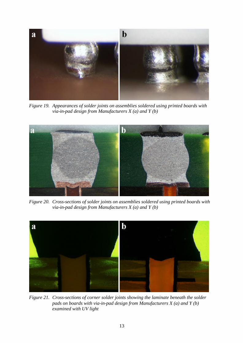
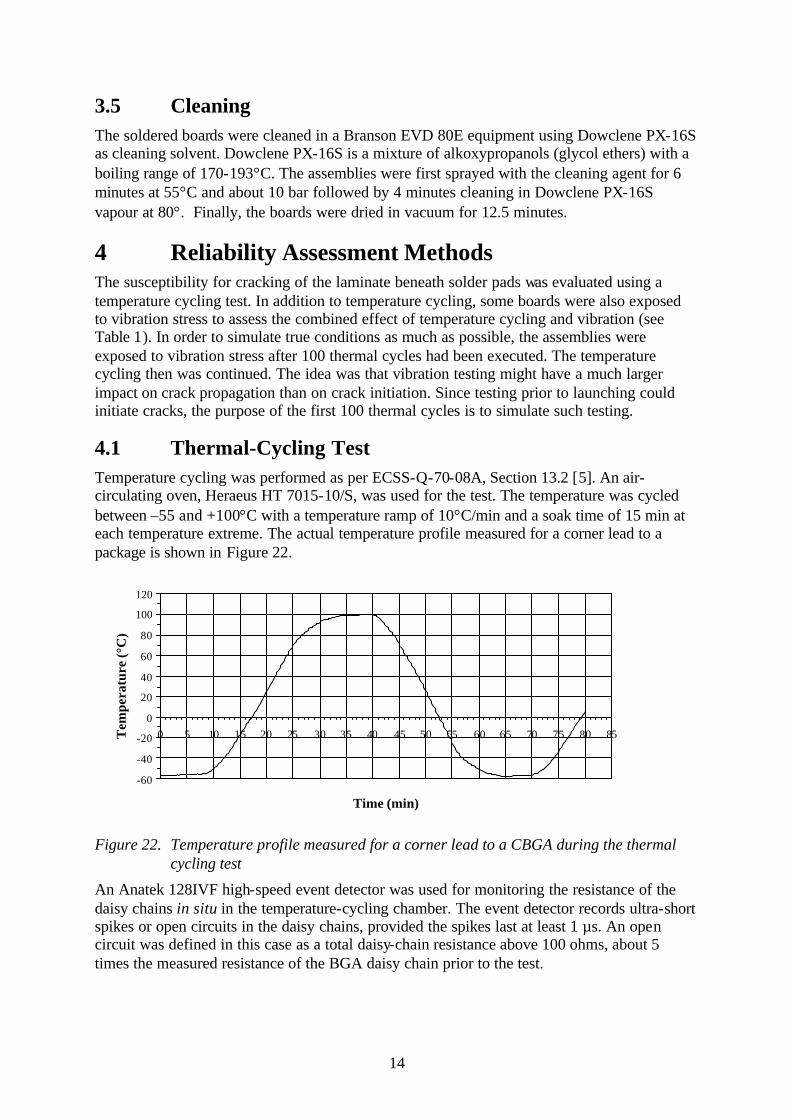
The appearances and cross-sections of typical solder joints are shown in Figures 19 and 20, respectively. The solder joints on the boards from Manufacturer X had an appearance similar to the solder joints on the boards with dogbone design, whereas a different appearance was observed for the solder joints on the boards from Manufacturer Y. Due to the larger pad diameter on these latter boards, the eutectic solder fillet between the board and the high-melt ball had a concave surface and not a convex surface as on the other boards. That is, whereas the smallest diameter of the solder fillets on the boards produced by Manufacturer Y was between the solder pads and the high-melt balls, it was at the base towards the printed board on the boards from Manufacturer X.
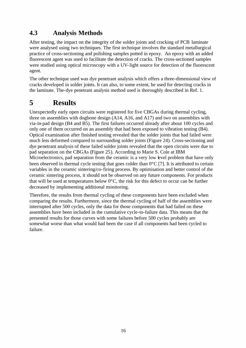
As for the assemblies manufactured with dogbone design, no cracks were found in the laminate beneath the solder pads on the assemblies with via- in-pad design after soldering (Figure 21).
Figure 18. Soldering profile used for the boards with via-in-pad design showing the temperature of the board, corner joint, and centre joint with temperature peaks of 248, 218, and 206°C, respectively
13
Figure 19. Appearances of solder joints on assemblies soldered using printed boards with
via-in-pad design from Manufacturers X (a) and Y (b)
Figure 20. Cross-sections of solder joints on assemblies soldered using printed boards with
via-in-pad design from Manufacturers X (a) and Y (b)
Figure 21. Cross-sections of corner solder joints showing the laminate beneath the solder
pads on boards with via-in-pad design from Manufacturers X (a) and Y (b) examined with UV light
14
3.5 Cleaning The soldered boards were cleaned in a Branson EVD 80E equipment using Dowclene PX-16S as cleaning solvent. Dowclene PX-16S is a mixture of alkoxypropanols (glycol ethers) with a boiling range of 170-193°C. The assemblies were first sprayed with the cleaning agent for 6 minutes at 55°C and about 10 bar followed by 4 minutes cleaning in Dowclene PX-16S vapour at 80°. Finally, the boards were dried in vacuum for 12.5 minutes.
4 Reliability Assessment Methods The susceptibility for cracking of the laminate beneath solder pads was evaluated using a temperature cycling test. In addition to temperature cycling, some boards were also exposed to vibration stress to assess the combined effect of temperature cycling and vibration (see Table 1). In order to simulate true conditions as much as possible, the assemblies were exposed to vibration stress after 100 thermal cycles had been executed. The temperature cycling then was continued. The idea was that vibration testing might have a much larger impact on crack propagation than on crack initiation. Since testing prior to launching could initiate cracks, the purpose of the first 100 thermal cycles is to simulate such testing.
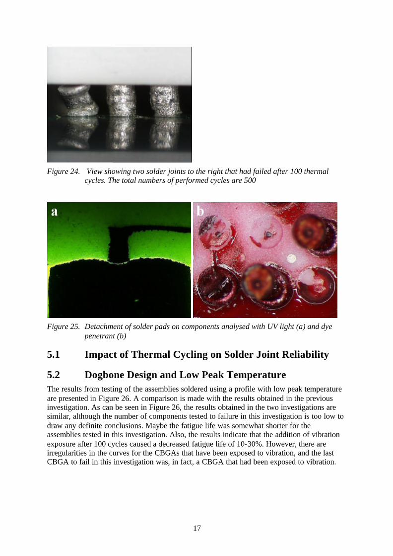
4.1 Thermal-Cycling Test Temperature cycling was performed as per ECSS-Q-70-08A, Section 13.2 [5]. An air-circulating oven, Heraeus HT 7015-10/S, was used for the test. The temperature was cycled between –55 and +100°C with a temperature ramp of 10°C/min and a soak time of 15 min at each temperature extreme. The actual temperature profile measured for a corner lead to a package is shown in Figure 22.
-60
-40
-20
0
20
40
60
80
100
120
0 5 10 15 20 25 30 35 40 45 50 55 60 65 70 75 80 85
Time (min)
Tem
pera
ture
(°C
)
Figure 22. Temperature profile measured for a corner lead to a CBGA during the thermal
cycling test
An Anatek 128IVF high-speed event detector was used for monitoring the resistance of the daisy chains in situ in the temperature-cycling chamber. The event detector records ultra-short spikes or open circuits in the daisy chains, provided the spikes last at least 1 µs. An open circuit was defined in this case as a total daisy-chain resistance above 100 ohms, about 5 times the measured resistance of the BGA daisy chain prior to the test.

15
A failure was defined as the first interruption of electrical continuity that is confirmed by 9 additional interruptions within an additional 10% of the cycle life per the recommendation in IPC-SM-785 [6].
Connections to the boards were made with wires soldered to the boards.
4.2 Vibration Test Sine and random vibration testing were performed using the conditions given in Table 2, which reflect the minimum severity for vibration testing given in Chapter 13 of ECSS-Q-70-08A [5]. The vibration testing was performed in two axes, one parallel to the long side of the test board and one perpendicular to the test board.
Table 2. Severity levels used for vibration testing
Frequency range 10-2000 Hz (CPS) at 15 g
Vibration amplitude (Peak to peak) 10-70 Hz at 1.5 mm
Sweep speed 1 octave per minute
Sine vibration
Duration 1 cycle from 10-2000-10 Hz
Frequency range 20-2000 Hz at 15 g (RMS)
Power spectral density 0.1 g2/Hz
Random vibration
Duration 10 min per axis
The test boards were fixed directly to the vibration board using five steel bars as shown in Figure 23. The screws were drawn with a moment of 0.25 – 0.27 Nm. Four product response accelerometers were attached to the test boards in the positions shown in Figure 23.
Figure 23. View of a test board with via-in-pad design mounted on the vibration exciter
16
4.3 Analysis Methods After testing, the impact on the integrity of the solder joints and cracking of PCB laminate were analysed using two techniques. The first technique involves the standard metallurgical practice of cross-sectioning and polishing samples potted in epoxy. An epoxy with an added fluorescent agent was used to facilitate the detection of cracks. The cross-sectioned samples were studied using optical microscopy with a UV-light source for detection of the fluorescent agent.
The other technique used was dye penetrant analysis which offers a three-dimensional view of cracks developed in solder joints. It can also, to some extent, be used for detecting cracks in the laminate. The-dye penetrant analysis method used is thoroughly described in Ref. 1.
5 Results Unexpectedly early open circuits were registered for five CBGAs during thermal cycling, three on assemblies with dogbone design (A14, A16, and A17) and two on assemblies with via-in-pad design (B4 and B5). The first failures occurred already after about 100 cycles and only one of them occurred on an assembly that had been exposed to vibration testing (B4). Optical examination after finished testing revealed that the solder joints that had failed were much less deformed compared to surrounding solder joints (Figure 24). Cross-sectioning and dye penetrant analysis of these failed solder joints revealed that the open circuits were due to pad separation on the CBGAs (Figure 25). According to Marie S. Cole at IBM Microelectronics, pad separation from the ceramic is a very low level problem that have only been observed in thermal cycle testing that goes colder than 0°C [7]. It is attributed to certain variables in the ceramic sintering/co-firing process. By optimisation and better control of the ceramic sintering process, it should not be observed on any future components. For products that will be used at temperatures below 0°C, the risk for this defect to occur can be further decreased by implementing additional monitoring.
Therefore, the results from thermal cycling of these components have been excluded when comparing the results. Furthermore, since the thermal cycling of half of the assemblies were interrupted after 500 cycles, only the data for those components that had failed on these assemblies have been included in the cumulative cycle-to-failure data. This means that the presented results for those curves with some failures before 500 cycles probably are somewhat worse than what would had been the case if all components had been cycled to failure.
17
Figure 24. View showing two solder joints to the right that had failed after 100 thermal
cycles. The total numbers of performed cycles are 500
Figure 25. Detachment of solder pads on components analysed with UV light (a) and dye
penetrant (b)
5.1 Impact of Thermal Cycling on Solder Joint Reliability
5.2 Dogbone Design and Low Peak Temperature The results from testing of the assemblies soldered using a profile with low peak temperature are presented in Figure 26. A comparison is made with the results obtained in the previous investigation. As can be seen in Figure 26, the results obtained in the two investigations are similar, although the number of components tested to failure in this investigation is too low to draw any definite conclusions. Maybe the fatigue life was somewhat shorter for the assemblies tested in this investigation. Also, the results indicate that the addition of vibration exposure after 100 cycles caused a decreased fatigue life of 10-30%. However, there are irregularities in the curves for the CBGAs that have been exposed to vibration, and the last CBGA to fail in this investigation was, in fact, a CBGA that had been exposed to vibration.

18
0102030405060708090
100
0 200 400 600 800 1000
Number of Thermal Cycles
Cum
ulat
ive
Fai
lure
Per
cent
ile .
Low peak, withvibration
Low peak, withoutvibration
Previous investigation,with vibration
Previous investigation,without vibration
Figure 26. Cumulative cycles-to-failure of CBGAs mounted on boards with dogbone design,
soldered with low peak temperature. For comparison, the corresponding results from the previous investigation are also given
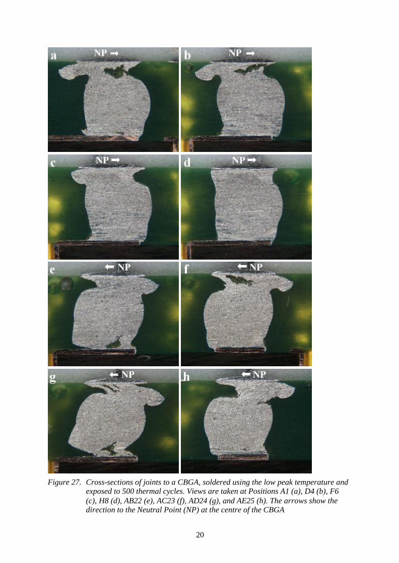
Figure 27 shows cross-sections of solder joints along the diagonal from Solder Joints A1 to AE25 for a CBGA that has been exposed to 500 thermal cycles but without vibration. The extent of deformation and cracking of the solder joints were identical to the results obtained in the previous investigation. When going from Solder Joint A1 towards the centre of the package, cracking and deformation of the solder joints are extensive for the first four joints and then decrease and are only just visible when reaching Solder Joint H8. The deformation and cracking are mainly located to the package side of the solder joints. The results are similar for Solder Joints AE25 and AC23 in the opposite corner of the package but quite different for Solder Joints AB24 and AD22. For these two latter solder joints, deformation and cracking have occurred both near the package and board sides of the solder joints, with the largest damage near the board side where the solder joints are almost completely cracked. When examining the board laminate under the solder pads using UV light, relatively large cracks were found in the laminate beneath the four outermost solder joints in the respective corner except for Solder Joints AB24 and AD22 (Figure 28). Small cracks in the laminate could be found beneath many solder pads five to ten solder joints from a corner. The cracks initiate on the inward side of the solder joints (the side towards the centre of the package). What differentiates Solder Joints AB24 and AD22 from the others is that the conductors to the interconnected via holes for these solder joints are located where the cracks initiate. Obviously, a conductor located there prevents a crack from initiating in the laminate.
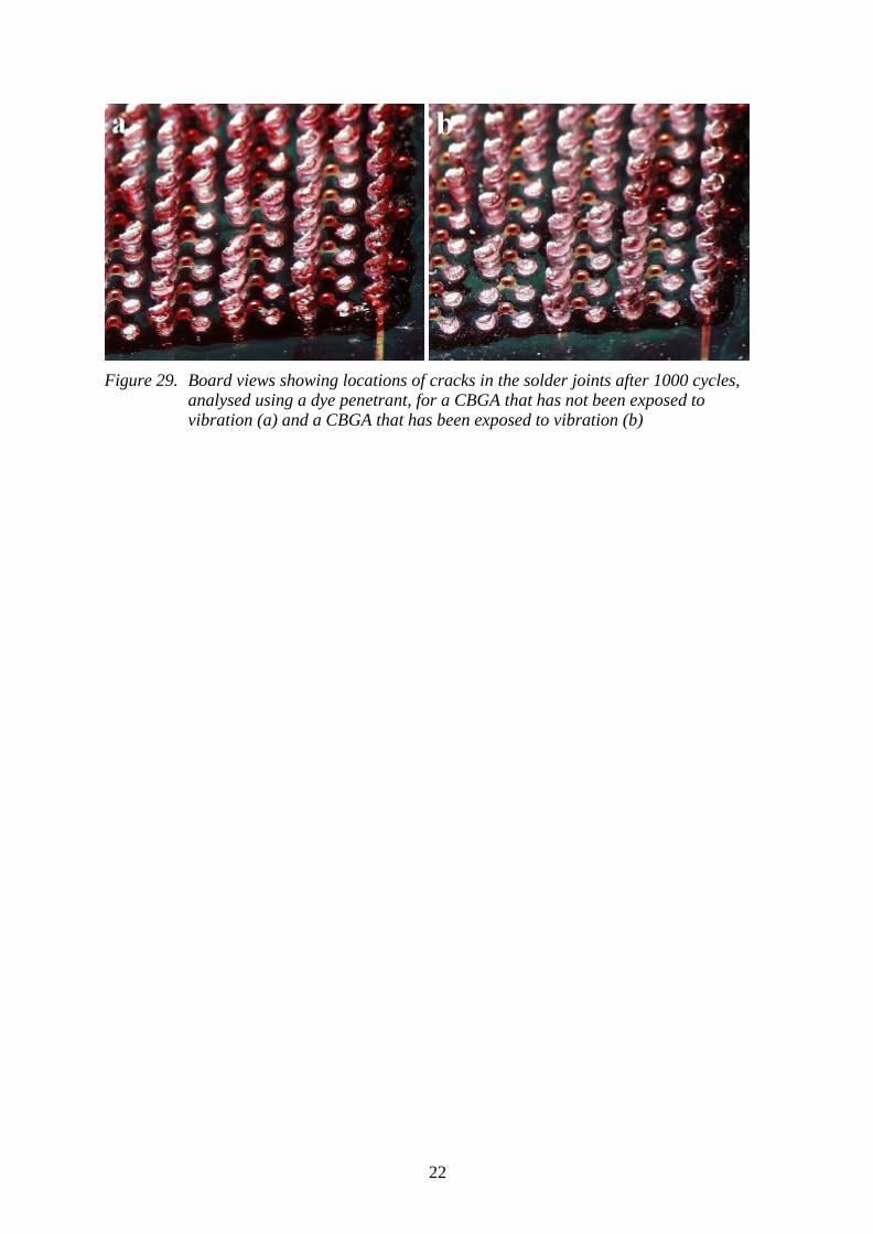
The locations of open joint s to the CBGAs on the assemblies that had been cycled 500 and 1000 cycles, respectively, were determined by probing the via holes from the backside of the boards. Almost all open joints were confined to solder joints having an inward interconnection to via holes. These can only be found on one side of the CBGAs, the side where row AE is located (see Figure 7). Clearly, the formation of cracks in the laminate beneath solder pads and the focusing of the main deformation and cracking of the solder joints towards the component pads are beneficial to fatigue life of the solder joints. In the absence of cracks in the laminate, deformation and cracking of solder joints occur both near the component and board pads but most severely near the board pads. A dye-penetrant test of a CBGA exposed to 1000 cycles confirmed this conclusion. When removing the CBGA, the majority of the solder balls remained attached to the board, indicating that the largest cracks in the solder joints were formed at the component side of the joints. Exceptions where the

19
locations were solder joints failed first, i.e. the solder joints that had board pads connected inwards to vias, for which the solder balls remained on the CBGA (Figure 29).
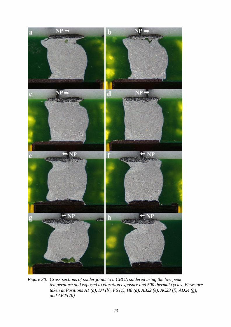
Figure 30 shows cross-sections of solder joints to a CBGA that had been exposed to vibration after 100 thermal cycles and then to an additional 400 thermal cycles. A comparison with the cross-sections shown in Figure 27 indicates that the addition of vibration caused somewhat less deformation of the solder joints to occur during thermal cycling. An exception is Solder Joint AD24 for which cracking was still severe against the board pad. Since only one vibration-tested and one non-vibration tested component have been cross-sectioned, the observed difference is uncertain but a visual examination of the outer solder joints to other components, using an optical microscope, indicated that the difference in deformation is consistent for all tested components.
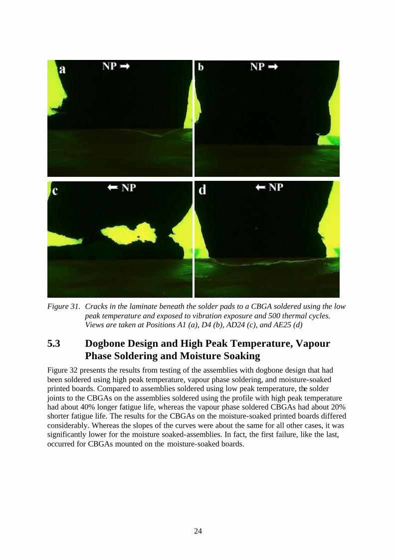
Cracks were also found in the laminate beneath solder pads for the CBGA that had been exposed to vibration (Figure 31) but the extent of cracking did not show any discernible difference compared to the CBGA that had not been exposed to vibration. Nor did the extent of solder joint cracking and the locations of fractures analysed using the dye penetrant method show any discernible difference (Figure 29b).
20
Figure 27. Cross-sections of joints to a CBGA, soldered using the low peak temperature and
exposed to 500 thermal cycles. Views are taken at Positions A1 (a), D4 (b), F6 (c), H8 (d), AB22 (e), AC23 (f), AD24 (g), and AE25 (h). The arrows show the direction to the Neutral Point (NP) at the centre of the CBGA

21
Figure 28. Cracks in the laminate beneath the solder pads to a CBGA soldered using the low
peak temperature and exposed to 500 thermal cycles. Views are taken at Positions A1 (a), D4 (b), F6 (c), AC23 (d), AD24 (e), and AE25 (f)
22
Figure 29. Board views showing locations of cracks in the solder joints after 1000 cycles,
analysed using a dye penetrant, for a CBGA that has not been exposed to vibration (a) and a CBGA that has been exposed to vibration (b)
23
Figure 30. Cross-sections of solder joints to a CBGA soldered using the low peak
temperature and exposed to vibration exposure and 500 thermal cycles. Views are taken at Positions A1 (a), D4 (b), F6 (c), H8 (d), AB22 (e), AC23 (f), AD24 (g), and AE25 (h)
24
Figure 31. Cracks in the laminate beneath the solder pads to a CBGA soldered using the low
peak temperature and exposed to vibration exposure and 500 thermal cycles. Views are taken at Positions A1 (a), D4 (b), AD24 (c), and AE25 (d)
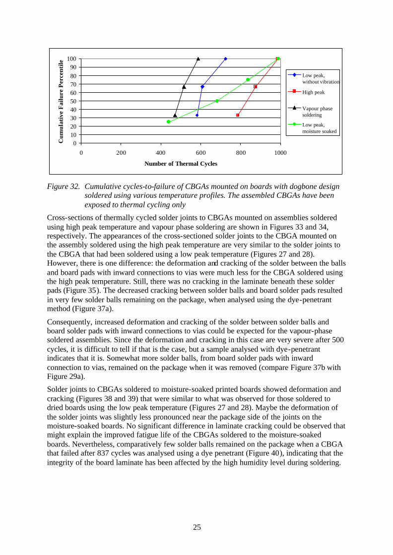
5.3 Dogbone Design and High Peak Temperature, Vapour Phase Soldering and Moisture Soaking
Figure 32 presents the results from testing of the assemblies with dogbone design that had been soldered using high peak temperature, vapour phase soldering, and moisture-soaked printed boards. Compared to assemblies soldered using low peak temperature, the solder joints to the CBGAs on the assemblies soldered using the profile with high peak temperature had about 40% longer fatigue life, whereas the vapour phase soldered CBGAs had about 20% shorter fatigue life. The results for the CBGAs on the moisture-soaked printed boards differed considerably. Whereas the slopes of the curves were about the same for all other cases, it was significantly lower for the moisture soaked-assemblies. In fact, the first failure, like the last, occurred for CBGAs mounted on the moisture-soaked boards.
25
0102030405060708090
100
0 200 400 600 800 1000
Number of Thermal Cycles
Cum
ulat
ive
Fai
lure
Per
cent
ile .
Low peak,without vibration
High peak
Vapour phasesoldering
Low peak,moisture soaked
Figure 32. Cumulative cycles-to-failure of CBGAs mounted on boards with dogbone design
soldered using various temperature profiles. The assembled CBGAs have been exposed to thermal cycling only
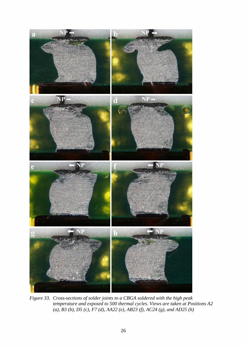
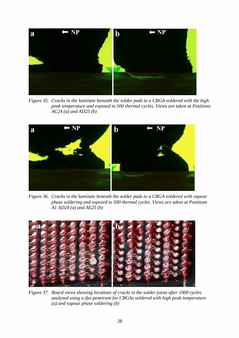
Cross-sections of thermally cycled solder joints to CBGAs mounted on assemblies soldered using high peak temperature and vapour phase soldering are shown in Figures 33 and 34, respectively. The appearances of the cross-sectioned solder joints to the CBGA mounted on the assembly soldered using the high peak temperature are very similar to the solder joints to the CBGA that had been soldered using a low peak temperature (Figures 27 and 28). However, there is one difference: the deformation and cracking of the solder between the balls and board pads with inward connections to vias were much less for the CBGA soldered using the high peak temperature. Still, there was no cracking in the laminate beneath these solder pads (Figure 35). The decreased cracking between solder balls and board solder pads resulted in very few solder balls remaining on the package, when analysed using the dye-penetrant method (Figure 37a).
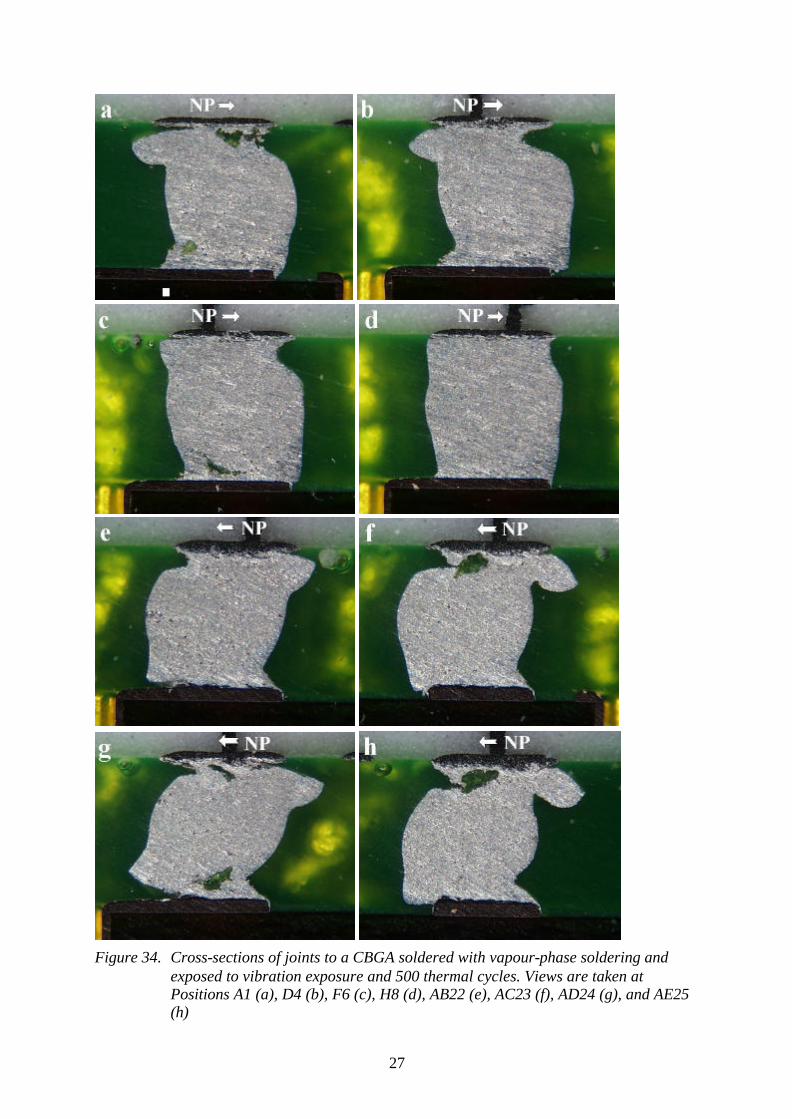
Consequently, increased deformation and cracking of the solder between solder balls and board solder pads with inward connections to vias could be expected for the vapour-phase soldered assemblies. Since the deformation and cracking in this case are very severe after 500 cycles, it is difficult to tell if that is the case, but a sample analysed with dye-penetrant indicates that it is. Somewhat more solder balls, from board solder pads with inward connection to vias, remained on the package when it was removed (compare Figure 37b with Figure 29a).
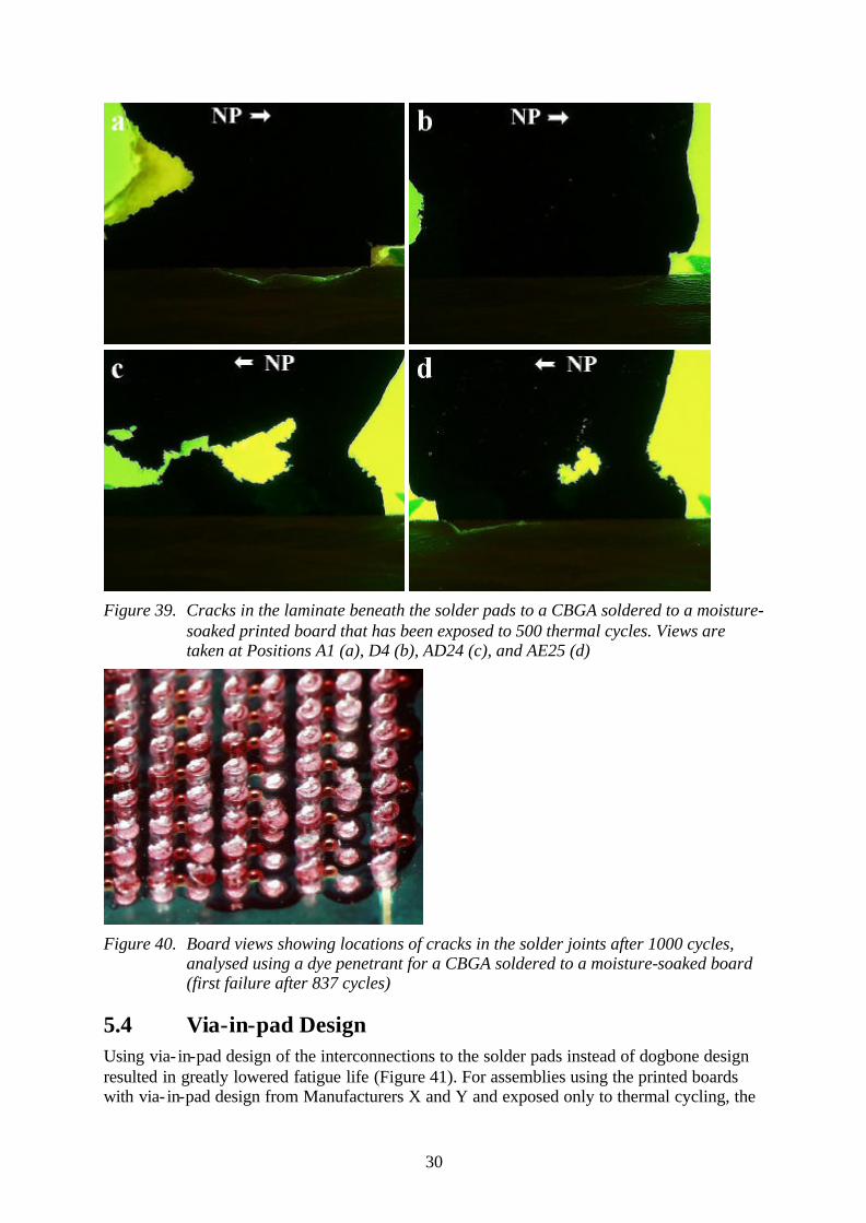
Solder joints to CBGAs soldered to moisture-soaked printed boards showed deformation and cracking (Figures 38 and 39) that were similar to what was observed for those soldered to dried boards using the low peak temperature (Figures 27 and 28). Maybe the deformation of the solder joints was slightly less pronounced near the package side of the joints on the moisture-soaked boards. No significant difference in laminate cracking could be observed that might explain the improved fatigue life of the CBGAs soldered to the moisture-soaked boards. Nevertheless, comparatively few solder balls remained on the package when a CBGA that failed after 837 cycles was analysed using a dye penetrant (Figure 40), indicating that the integrity of the board laminate has been affected by the high humidity level during soldering.
26
Figure 33. Cross-sections of solder joints to a CBGA soldered with the high peak
temperature and exposed to 500 thermal cycles. Views are taken at Positions A2 (a), B3 (b), D5 (c), F7 (d), AA22 (e), AB23 (f), AC24 (g), and AD25 (h)
27
Figure 34. Cross-sections of joints to a CBGA soldered with vapour-phase soldering and
exposed to vibration exposure and 500 thermal cycles. Views are taken at Positions A1 (a), D4 (b), F6 (c), H8 (d), AB22 (e), AC23 (f), AD24 (g), and AE25 (h)
28
Figure 35. Cracks in the laminate beneath the solder pads to a CBGA soldered with the high
peak temperature and exposed to 500 thermal cycles. Views are taken at Positions AC24 (a) and AD25 (b)
Figure 36. Cracks in the laminate beneath the solder pads to a CBGA soldered with vapour
phase soldering and exposed to 500 thermal cycles. Views are taken at Positions A1 AD24 (a) and AE25 (b)
Figure 37. Board views showing locations of cracks in the solder joints after 1000 cycles
analysed using a dye penetrant for CBGAs soldered with high peak temperature (a) and vapour phase soldering (b)

29
Figure 38. Cross-sections of solder joints to a CBGA soldered to a moisture-soaked printed
board and exposed to 500 thermal cycles. Views are taken at Positions A1 (a), D4 (b), F6 (c), H8 (d), AB22 (e), AC23 (f), AD24 (g), and AE25 (h)
30
Figure 39. Cracks in the laminate beneath the solder pads to a CBGA soldered to a moisture-
soaked printed board that has been exposed to 500 thermal cycles. Views are taken at Positions A1 (a), D4 (b), AD24 (c), and AE25 (d)
Figure 40. Board views showing locations of cracks in the solder joints after 1000 cycles,
analysed using a dye penetrant for a CBGA soldered to a moisture-soaked board (first failure after 837 cycles)
5.4 Via-in-pad Design Using via- in-pad design of the interconnections to the solder pads instead of dogbone design resulted in greatly lowered fatigue life (Figure 41). For assemblies using the printed boards with via- in-pad design from Manufacturers X and Y and exposed only to thermal cycling, the

31
fatigue life decreased with about 30% and 65%, respectively, compared to assemblies with dogbone design.
0102030405060708090
100
0 200 400 600 800 1000
Number of Thermal Cycles
Cum
ulat
ive
Fai
lure
Per
cent
ile .
Manufacturer X,with vibrationManufacturer X,without vibrationManufacturer Y,with vibrationManufacturer Y,without vibrationLow peak, withvibrationLow peak, withoutviabration
Figure 41. Cumulative cycles-to-failure of CBGAs mounted on boards with via-in-pad
design. The results for CBGAs mounted on boards with dogbone design, soldered with low peak temperature, are given as reference
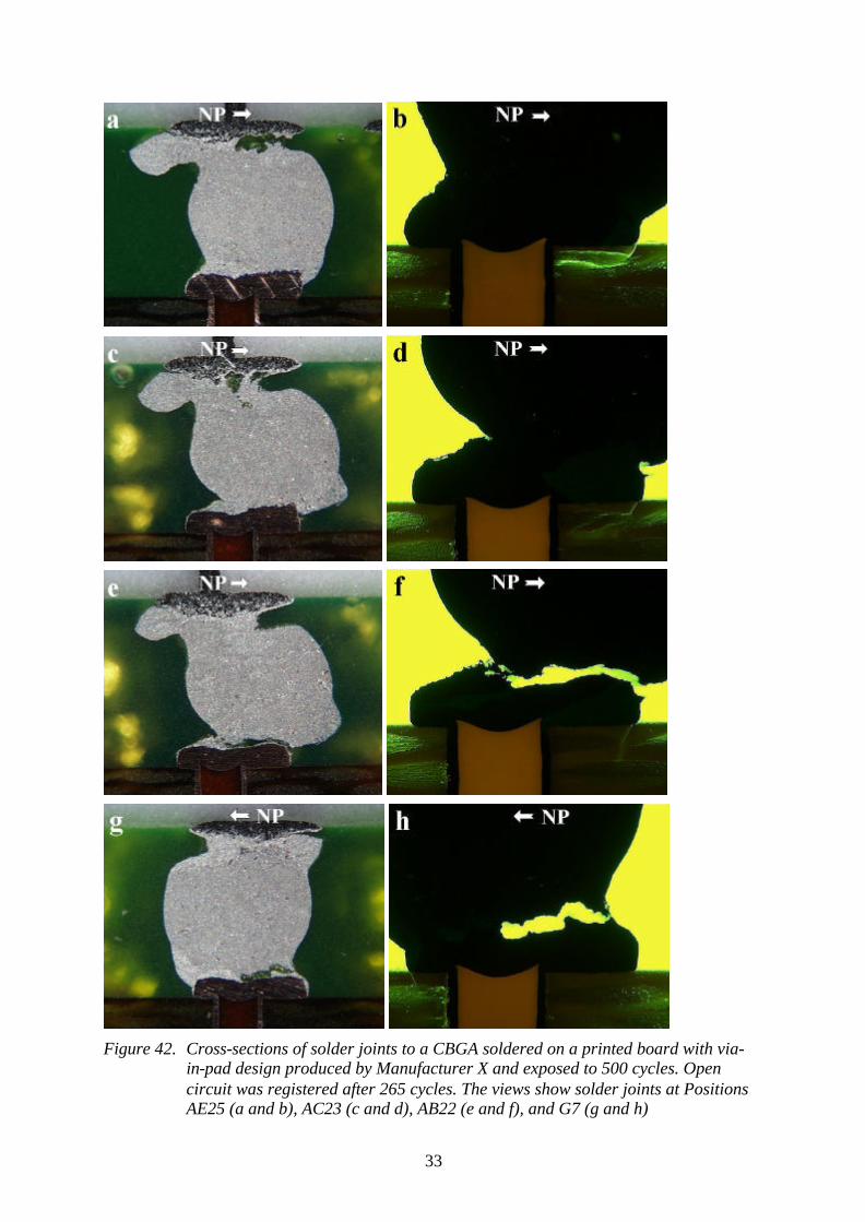
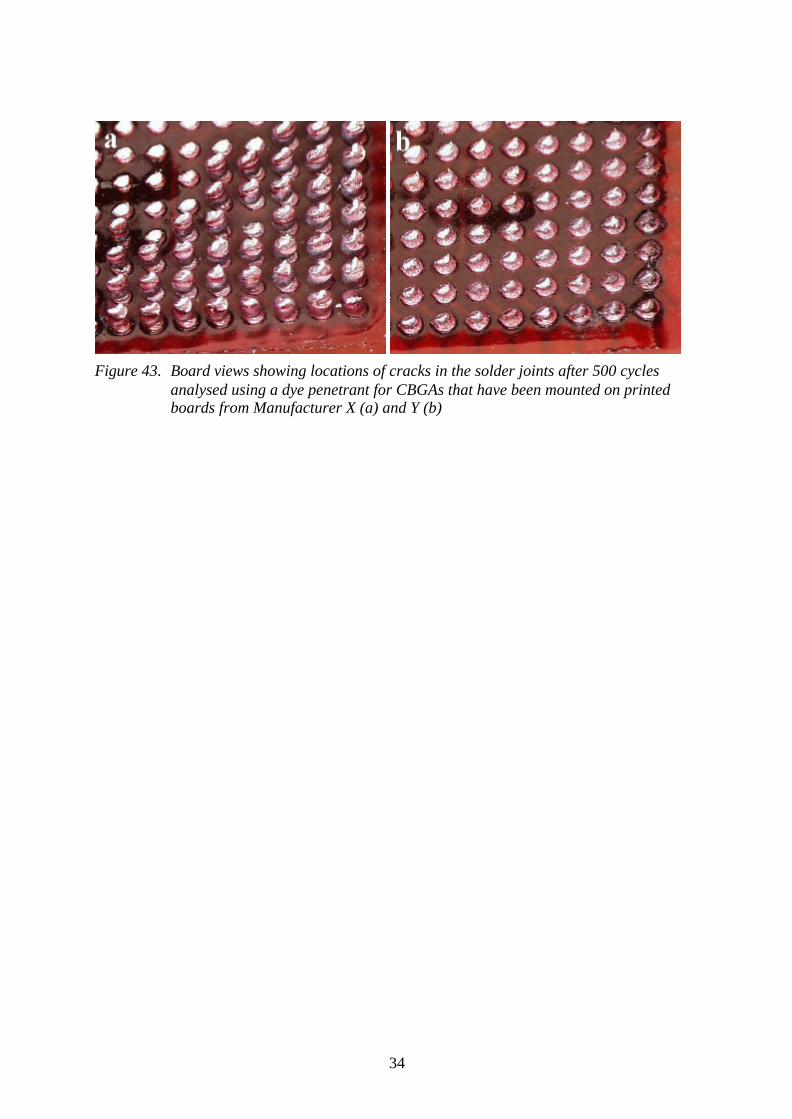
Cross-sections of solder joints to a CBGA mounted on a printed board with via- in-pad design from Manufacturer X and exposed to 500 cycles are shown in Figure 42. Corner solder joints have deformation and cracking similar to what was observed for corner joints to CBGAs mounted on boards with dogbone design having outward connection to the vias. Extensive cracking was observed in the board laminate beneath these solder joints, and the main deformation and cracking of the solder joints occurred between the balls and the solder pads on the component. This behaviour gradually changed when going inward from a corner solder joint and the cracking behaviour became more similar to solder joints on solder pads with inward connection to vias on boards with dogbone design. That is, four to six solder joints inwards from a corner, the cracks in the laminate were very small and almost all deformation and cracking in the solder joints occurred between the balls and solder pads on the board. In fact, some of the largest cracks in solder joints were found here and, probably, the first open circuits occurred here (probing showed that failure had not occurred in the two outer rows). This behaviour was also reflected on samples that were analysed using the dye penetrant. Corner solder balls remained on the board, whereas balls closer to the package centre remained on the package (Figure 43a).
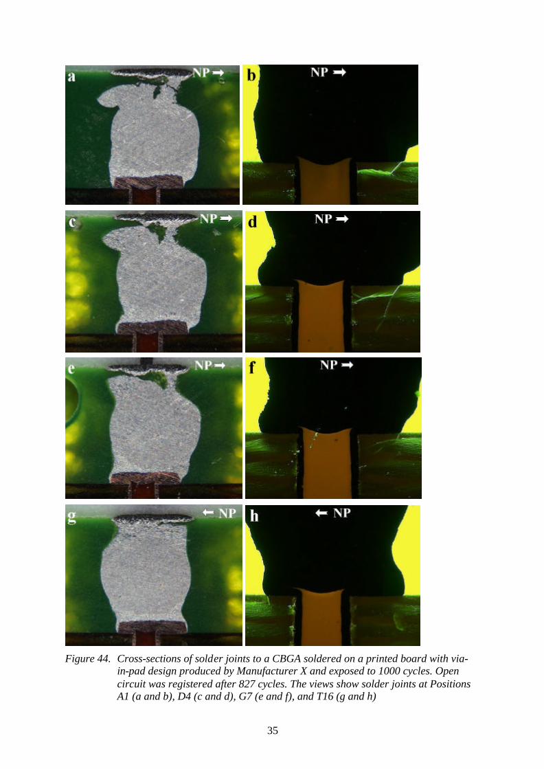
Two CBGAs mounted on printed boards from Manufacturer X had an unexpectedly long fatigue life, one on an assembly that had been exposed to vibration and one on an assembly that had not been vibrated. Cross-sections of solder joints to the CBGA on the latter assembly revealed that there were no solder joints with large cracks between solder balls and board solder pads for this component (Figure 44). All major cracks were found near the component pads. A comparison of the cross-sections of solder joints in Figures 42 and 44 indicates that the solder has wetted the edges of the board pads better in the latter case, which has probably affected the diameter of the solder joint fillet and the distribution of stresses during thermal cycling.
The manner of cracking of the solder joints to CBGAs mounted on printed boards from Manufacturer Y differed noticeably compared to those mounted on printed boards from Manufacturer X. The main deformation and cracking of solder joints occurred between the balls and the solder pads on the board, even for corner solder joints, and cracking occurred to

32
a very small extent in the laminate beneath solder pads (Figure 45). For a component that was analysed with dye penetrant, all except one solder ball remained on the package (Figure 43b).
In contrast to the assemblies with dogbone design, exposure to vibration improved the fatigue life of the solder joints to CBGAs mounted on boards with via- in-pad design (see Figure 41). In the case of CBGAs mounted on printed boards from Manufacturer X, it was observed that the exposure to vibration caused increased cracking of the laminate beneath the solder pads (Figure 46). This diminished the deformation and cracking of the solder joints, especially three to six solder joints inward from corner joints, which is the likely cause of the improved fatigue life. For some corner joints, not just the laminate had cracked but also the connection between the plating in the vias and the solder pads. This could also be observed on a sample analysed using dye penetrant (Figure 47).
It was not as clear for the CBGAs mounted on printed boards from Manufacturer Y that exposure to vibration increased the cracking of the board laminate, but it could be observed that the deformation and cracking of the solder joints decreased between the balls and the solder pads on the board. At the same time, the deformation and cracking increased between the balls and the solder pads on the package (Figure 48) and 36 balls remained on the board for a component analysed using dye penetrant.
33
Figure 42. Cross-sections of solder joints to a CBGA soldered on a printed board with via-
in-pad design produced by Manufacturer X and exposed to 500 cycles. Open circuit was registered after 265 cycles. The views show solder joints at Positions AE25 (a and b), AC23 (c and d), AB22 (e and f), and G7 (g and h)
34
Figure 43. Board views showing locations of cracks in the solder joints after 500 cycles
analysed using a dye penetrant for CBGAs that have been mounted on printed boards from Manufacturer X (a) and Y (b)
35
Figure 44. Cross-sections of solder joints to a CBGA soldered on a printed board with via-
in-pad design produced by Manufacturer X and exposed to 1000 cycles. Open circuit was registered after 827 cycles. The views show solder joints at Positions A1 (a and b), D4 (c and d), G7 (e and f), and T16 (g and h)
36
Figure 45. Cross-sections of solder joints to a CBGA soldered on a printed board with via-
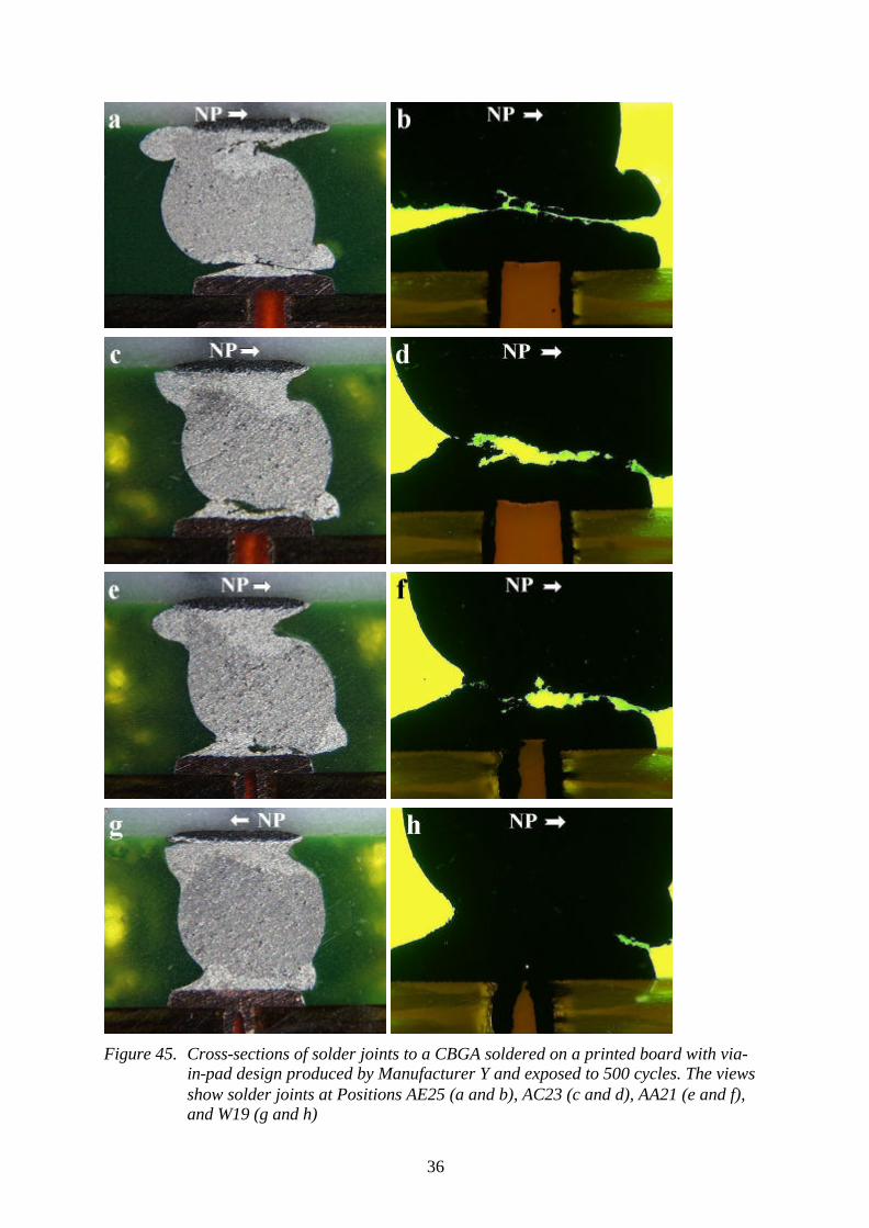
in-pad design produced by Manufacturer Y and exposed to 500 cycles. The views show solder joints at Positions AE25 (a and b), AC23 (c and d), AA21 (e and f), and W19 (g and h)
37
Figure 46. Cross-sections of joints to a CBGA soldered on a printed board with via-in-pad
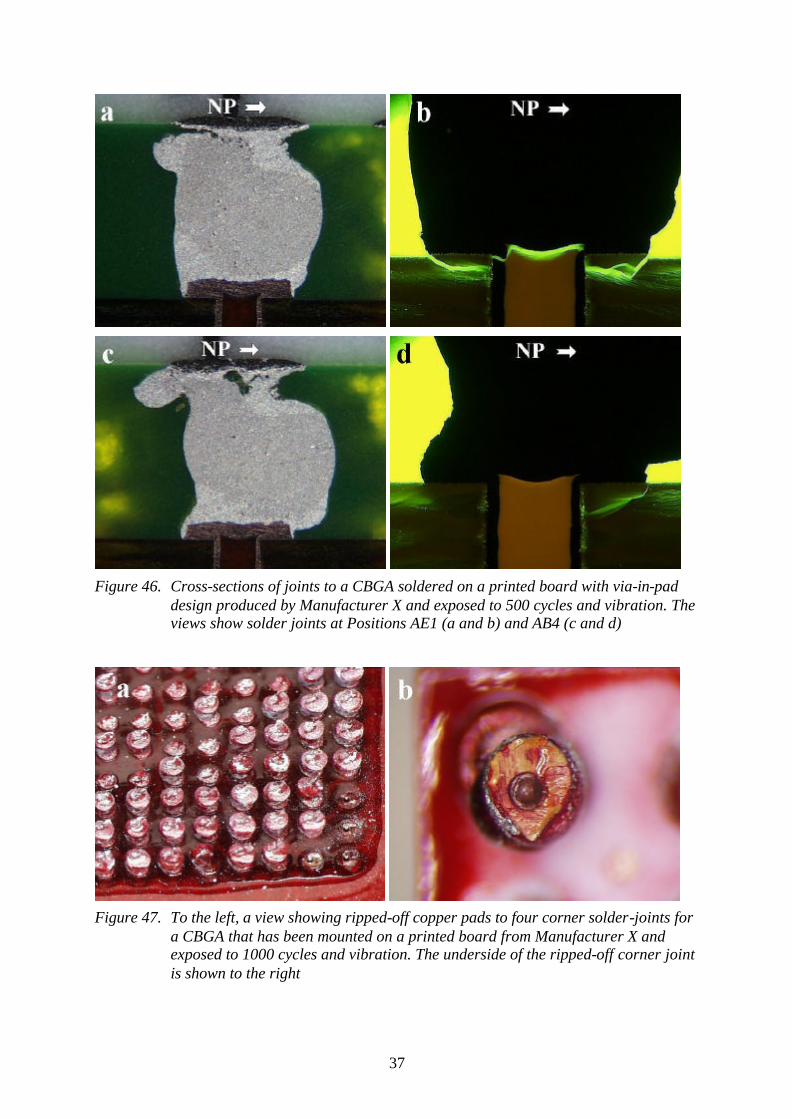
design produced by Manufacturer X and exposed to 500 cycles and vibration. The views show solder joints at Positions AE1 (a and b) and AB4 (c and d)
Figure 47. To the left, a view showing ripped-off copper pads to four corner solder-joints for
a CBGA that has been mounted on a printed board from Manufacturer X and exposed to 1000 cycles and vibration. The underside of the ripped-off corner joint is shown to the right
38
Figure 48. Cross-sections of solder joints to a CBGA on a printed board with via-in-pad
design produced by Manufacturer Y and exposed to 500 cycles and vibration. The views show solder joints at Positions A2 (a and b) and D5 (c and d)
6 Discussion
6.1 Factors Affecting Board Laminate Cracking Main goals of this investigation were to find the causes for formation of cracks in the board laminate and their effects on reliability. With the exception of assemblies soldered with a high peak temperature, the fatigue life of the CBGAs mounted on the boards with dogbone design was determined by the fatigue life of the solder joints with board pads interconnected inwards to vias. No cracking of the laminate was observed beneath these pads on any of the test vehicles, not even in those soldered with high peak temperature. Unfortunately, this makes it more difficult to conclude how the various parameters studied affected laminate cracking and the impact of laminate cracking on the fatigue life of solder joints.
Nevertheless, since all boards with dogbone design had about the same amount of laminate cracking, the results indicate that laminate cracking is not significantly affected by the soldering profile. Furthermore, the results for the assemblies with dogbone design soldered with low peak temperature are essentially identical with the results achieved in the previous investigation, in regard to fatigue life, deformation and cracking of solder joints, and cracking of board laminate. Thus, the high stress that the board laminate is exposed to during HASL (used in the previous investigation) does not seem to increase the extent of laminate cracking.
39
One parameter not subject to this investigation, but possibly of major importance, is the low temperature extreme during thermal cycling. The locations of the cracks in the laminate on the inward side of the solder pads indicate that they are formed during the cooling phase of the thermal cycle. Since stress relaxation and creep of solder practically cease below -20°C [6], the stress level transmitted to the laminate will basically be proportional to how far the low temperature extreme is below -20°C. Furthermore, the polyimide polymer will be more brittle and harder at lower temperatures. Thus, the likelihood for laminate cracking can be expected to increase with lower temperature extremes. Since laminate cracking likely improves the fatigue life of the solder joints, this implies that the fatigue life may be considerably shorter if a higher temperature is chosen as the low temperature extreme. That is, it is possible that the temperature cycling range required by ECSS-Q-70-08A may lead to greatly overestimated fatigue life for products used in more benign environments. In most investigations performed on solder-joint fatigue, the low temperature extreme is selected in the interval -40 to 0°C. This may be the reason why rather little is reported on laminate cracking in literature. Another reason may be that laminate cracking is difficult to detect if one does not specifically look for it. It requires that the sample is potted in epoxy with an added fluorescent agent and that inspection is done with UV light.
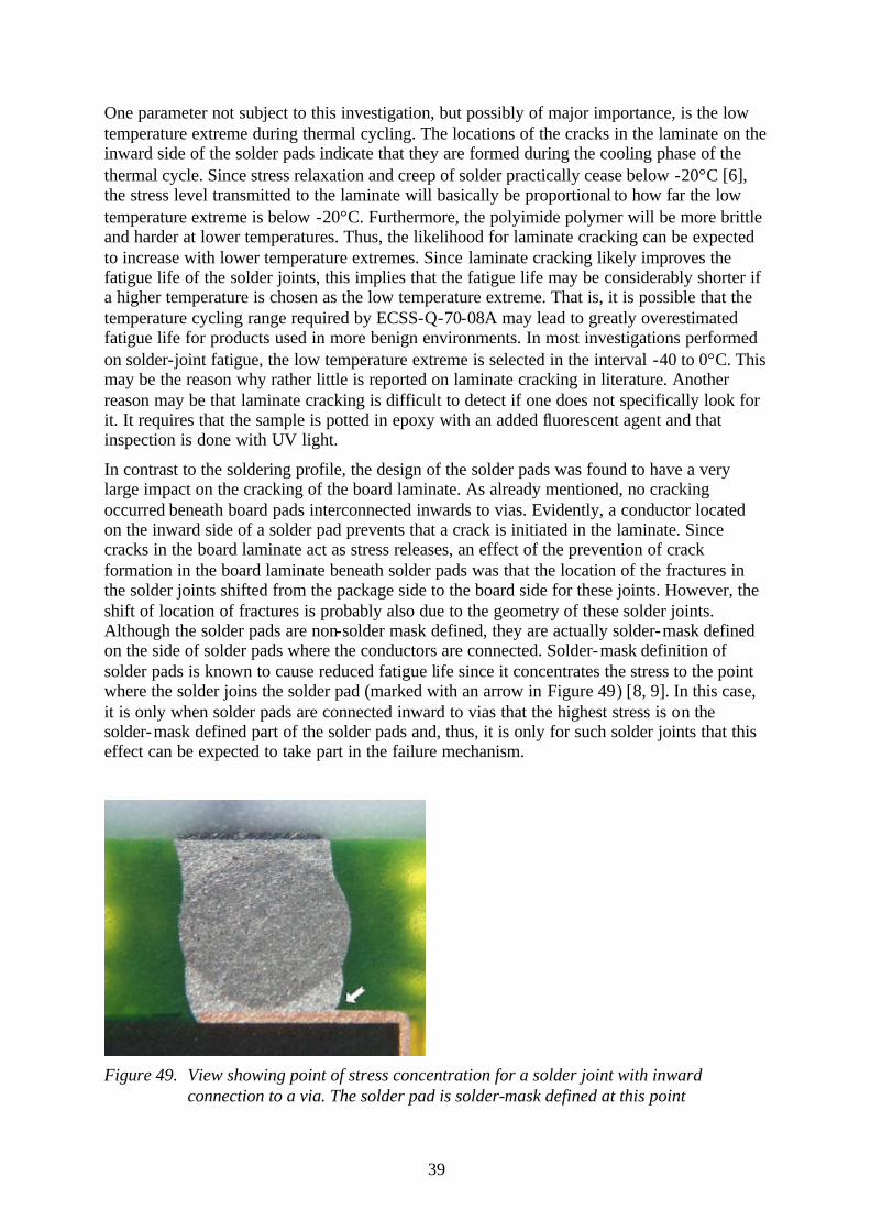
In contrast to the soldering profile, the design of the solder pads was found to have a very large impact on the cracking of the board laminate. As already mentioned, no cracking occurred beneath board pads interconnected inwards to vias. Evidently, a conductor located on the inward side of a solder pad prevents that a crack is initiated in the laminate. Since cracks in the board laminate act as stress releases, an effect of the prevention of crack formation in the board laminate beneath solder pads was that the location of the fractures in the solder joints shifted from the package side to the board side for these joints. However, the shift of location of fractures is probably also due to the geometry of these solder joints. Although the solder pads are non-solder mask defined, they are actually solder-mask defined on the side of solder pads where the conductors are connected. Solder-mask definition of solder pads is known to cause reduced fatigue life since it concentrates the stress to the point where the solder joins the solder pad (marked with an arrow in Figure 49) [8, 9]. In this case, it is only when solder pads are connected inward to vias that the highest stress is on the solder-mask defined part of the solder pads and, thus, it is only for such solder joints that this effect can be expected to take part in the failure mechanism.
Figure 49. View showing point of stress concentration for a solder joint with inward
connection to a via. The solder pad is solder-mask defined at this point
40
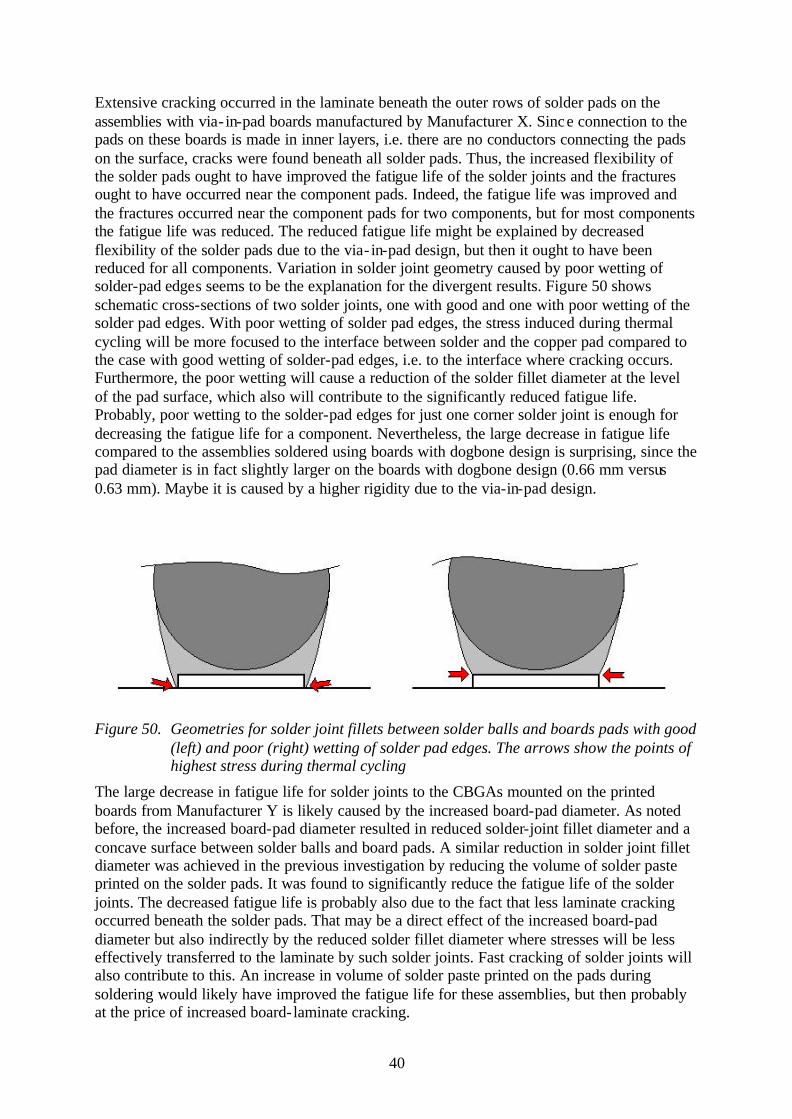
Extensive cracking occurred in the laminate beneath the outer rows of solder pads on the assemblies with via- in-pad boards manufactured by Manufacturer X. Since connection to the pads on these boards is made in inner layers, i.e. there are no conductors connecting the pads on the surface, cracks were found beneath all solder pads. Thus, the increased flexibility of the solder pads ought to have improved the fatigue life of the solder joints and the fractures ought to have occurred near the component pads. Indeed, the fatigue life was improved and the fractures occurred near the component pads for two components, but for most components the fatigue life was reduced. The reduced fatigue life might be explained by decreased flexibility of the solder pads due to the via- in-pad design, but then it ought to have been reduced for all components. Variation in solder joint geometry caused by poor wetting of solder-pad edges seems to be the explanation for the divergent results. Figure 50 shows schematic cross-sections of two solder joints, one with good and one with poor wetting of the solder pad edges. With poor wetting of solder pad edges, the stress induced during thermal cycling will be more focused to the interface between solder and the copper pad compared to the case with good wetting of solder-pad edges, i.e. to the interface where cracking occurs. Furthermore, the poor wetting will cause a reduction of the solder fillet diameter at the level of the pad surface, which also will contribute to the significantly reduced fatigue life. Probably, poor wetting to the solder-pad edges for just one corner solder joint is enough for decreasing the fatigue life for a component. Nevertheless, the large decrease in fatigue life compared to the assemblies soldered using boards with dogbone design is surprising, since the pad diameter is in fact slightly larger on the boards with dogbone design (0.66 mm versus 0.63 mm). Maybe it is caused by a higher rigidity due to the via-in-pad design.
Figure 50. Geometries for solder joint fillets between solder balls and boards pads with good
(left) and poor (right) wetting of solder pad edges. The arrows show the points of highest stress during thermal cycling
The large decrease in fatigue life for solder joints to the CBGAs mounted on the printed boards from Manufacturer Y is likely caused by the increased board-pad diameter. As noted before, the increased board-pad diameter resulted in reduced solder-joint fillet diameter and a concave surface between solder balls and board pads. A similar reduction in solder joint fillet diameter was achieved in the previous investigation by reducing the volume of solder paste printed on the solder pads. It was found to significantly reduce the fatigue life of the solder joints. The decreased fatigue life is probably also due to the fact that less laminate cracking occurred beneath the solder pads. That may be a direct effect of the increased board-pad diameter but also indirectly by the reduced solder fillet diameter where stresses will be less effectively transferred to the laminate by such solder joints. Fast cracking of solder joints will also contribute to this. An increase in volume of solder paste printed on the pads during soldering would likely have improved the fatigue life for these assemblies, but then probably at the price of increased board- laminate cracking.
41
Whereas vibration exposure decreased the fatigue life for the assemblies with dogbone design, it improved the fatigue life of the assemblies with via- in-pad design. The explanation for this difference can probably be found in different board- laminate cracking behaviour. The fatigue life determining solder joints on the assemblies with dogbone design had no cracks in the laminate beneath the solder pads, neither before nor after vibration exposure. The only effect of the vibration exposure then has been that some of the fatigue life of the solder joints has been taken. In contrast, the vibration exposure of the assemblies with via- in-pad design manufactured using printed boards from Manufacturer X increased the amount of laminate cracking. Thus, in addition to taking some of the fatigue life of the solder joints, it increases the flexibility of the board pads, which improves the fatigue life. For these assemblies, the latter effect has been dominating. Although the assemblies manufactured using printed boards from Manufacturer Y do not show any clear evidence of increased laminate cracking, there are cracks in the laminate beneath the board pads for these assemblies and it is likely that they have been affected by the vibration exposure.
Laminate cracking does not merely affect reliability by its influence on fatigue life of solder joints. For the assemblies with via- in-pad design boards produced by Manufacturer X, laminate cracking resulted also in fractures between via-hole plating and solder pads, at least for the assemblies that had been exposed to vibration. Unfortunately, it is impossible to tell whether open circuits have been due to solder-joint fatigue or via-barrel cracking. Anyhow, failures have not occurred in connection with vibration exposure, but long afterwards and, since the CBGAs that had been exposed to vibration had the longest fatigue life, barrel cracking is probably not the dominating cause of open circuits.
The enhanced fatigue life for the assemblies soldered using moisture-soaked printed boards indicates that increased water content in printed boards during soldering affects the failure mechanism. Microsections of thermally cycled solder joints do not reveal what may cause the improved fatigue life, but the increased water content likely affects the integrity of the polyimide resin in a way that makes the laminate more flexible. However, since one of the components failed already after 438 cycles and the slope of the curve in Figure 32 is low, the results are not conclusive.
6.2 Dissolution of Lead into Eutectic Solder Although an increase of the peak temperature during soldering did not seem to affect the cracking of the board laminate, it had a large impact on the fatigue life of the solder joints. There are two plausible explanations for this finding. The increased peak temperature may have induced microcracks in the laminate beneath solder pads that may cause faster and more extensive laminate cracking during thermal cycling. However, microsections of thermally cycled solder joints do not show any signs indicating that this should be the case. Another more likely explanation is that the improved fatigue life is due to increased dissolution of lead from the high-melt ball into the eutectic solder. This will increase the melting point of the once eutectic solder: the more lead dissolved, the higher the melting point. An increase in melting point will likely make the solder more resistant against creep and consequently also against deformation. In fact, for solder joints with inward connection to vias, the most severe deformation occurred near the board pads when the assemblies had been soldered using low peak temperature. Since the eutectic solder joints near the component pads have undergone two soldering processes (the first attaching the solder balls), whereas the eutectic solder joints near the board pads have only undergone one, the latter should have a lower melting point. An increase in peak temperature will diminish the difference in melting point. This is consistent with the finding that the fractures for solder joints with inward connection to vias moved from the board side to the component side for the assemblies soldered using the high peak
42
temperature. Thus, an increased peak temperature not only improves fatigue life, but also affects where the fracture occurs for ceramic BGAs with high-melt solder balls.
The reduced fatigue life for the vapour-phase soldered components has probably the same explanation but in this case less lead has been dissolved into the eutectic solder. That is, the increase in melting point is less than for the packages soldered using the low peak temperature. The actual temperature profile during vapour-phase soldering was not measured. However, although the peak temperature was probably slightly higher during vapour-phase soldering, the cooling rate was probably faster (Figure 14), which might have caused less dissolution of lead. Cross-sections of thermally cycled solder joints do not show any significant differences between vapour-phase soldered joints and joints soldered using the low peak temperature that might support this assumption. However, the increased number of fractures near board pads for the vapour-phase soldered package analysed with dye penetrant (Figure 37) indicates that the assumption might be correct.
6.3 Impact on Reliability The results from this investigation indicate that cracking of the printed board laminate beneath solder pads to large CBGAs is difficult to avoid, at least when thermal cycling is done down to -55°C. The only effective measure to prevent laminate cracking was to connect the solder pad with an inward conductor. Even if via- in-pad is used, this could be achieved by using short “blind” conductors. However, some cracking of the board laminate is beneficial for the fatigue life since it will reduce the stress on the solder joints due to thermal mismatch. Therefore, effective prevention of laminate cracking will decrease the fatigue life of the solder joints. An increase of solder pad diameter decreases the extent of laminate cracking but also, in this case, at the cost of decreased fatigue life of the solder joints.
The solder-pad diameter versus solder paste volume must be carefully optimised for optimum fatigue life. Also, the impact on the melting point of the eutectic solder by dissolution of lead from the high-melt ball into the eutectic solder must be considered. Best fatigue life of solder joints is achieved if deformation and cracking occur to about the same extent near package and board pads. Since the solder fillet on the package side has higher melting point due to more lead dissolution from the high-melt ball, it may be advantageous to use a higher peak temperature during soldering in order to minimise the difference in melting point of the two solder fillets. However, this will make repair and rework more difficult. Another possibility is to increase the board-pad diameter.
These measures are valid if there is no cracking of the board laminate since cracking of board laminate will change the situation. Cracking of board laminate will cause the main deformation and cracking of the solder joint to occur near the component pad. Increasing peak temperature during soldering or increasing pad diameter will then probably exaggerate cracking at the component pad. Instead, the peak temperature should probably be as low as possible and perhaps the pad diameter should be decreased in this case.
7 Conclusions 1 The low temperature extreme during thermal cycling is probably one of the main causes
for cracking of printed board laminate beneath solder pads to ceramic BGAs.
2 Hot air solder levelling (HASL) and the soldering profile used during reflow soldering of assemblies do not significantly affect the extent of cracking of the printed board laminate. Nevertheless, increased peak temperature during reflow soldering may improve the fatigue
43
life of solder joints due to an increase of the melting point of the eutectic solder fillet between solder ball and board pad.
3 Pad design has a large impact on the extent of board laminate cracking. An effective measure to prevent laminate cracking is to connect the pad with an inward conductor. Another alternative, but less effective, is to increase board pad diameter.
4 Board laminate cracking is beneficial for solder joint fatigue life. Measures to reduce laminate cracking will likely cause reduced fatigue life but might be necessary in order to prevent other failure mechanisms, such as current leakage caused by contamination and humidity.
5 Optimisation of board pad diameter versus solder-paste volume is important for achieving optimum solder-joint life. The solder fillet between the high-melt solder ball and the board pad should have a convex surface. Good wetting of solder pad edges is essential for optimum fillet geometry.
6 Cracking of board laminate may cause fracture of the plating in via holes beneath solder pads if via-in-pad design is used.
7 Vibration exposure after some thermal cycling may actually improve the fatigue life of solder joints if cracks have formed in the board laminate. Otherwise, the fatigue life may be shortened.
8 Acknowledgements The work performed in this report was funded by the European Space Agency through its European Space Research and Technology Centre.
9 References 1 P.-E. Tegehall and B. D. Dunn, Assessment of the Reliability of Solder Joints to Ball
and Column Grid Array Packages for Space Applications, ESA STM-266, ESA Publications Division, Noordwijk, 2001.
2 IPC-7095, Design and Assembly Process Implementation for BGAs, IPC, August 2000. 3 C. Milkovich and L. Jimarez, Ceramic Ball Grid Array Surface Mount Assembly and
Rework, Document APD-SBSC-101.0, IBM Corporation, 1998. 4 IPC/JEDEC J-STD-020B, Moisture/Reflow Sensitivity Classification for Nonhermetic
Solid State Surface Mount Devices, IPC, July 2002. 5 ECSS-Q-70-08A, The manual soldering of high-reliability electrical connections, ESA
Pub-SM-785, Guidelines for Accelerated Reliability Testing of Surface Mount Solder Attachments Publication Division, Noordwijk, The Netherlands, August 1999.
6 IPC, IPC, November 1992. 7 Marie S. Cole, IBM Microelectronics, Hopewell Jct, New York, Private
correspondence. 8 A. Mawer, D. Cho and R. Darveaux, The Effect of PBG Solder Pad Geometry on Solder
Joint Reliability, Proc. Surface Mount International, pp. 127-135, 1996. 9 R. Rörgren, P.-E. Tegehall, and P. Carlsson, Reliability of Ball Grid Array Packages in
an Automotive Environment, Proc. Surface Mount International, San José, pp. 85-92, 1997