Embed Size (px)
Citation preview
146 IEEE ELECTRON DEVICE LETTERS, VOL. 32, NO. 2, FEBRUARY 2011
III–V Multiple-Gate Field-Effect Transistors WithHigh-Mobility In0.7Ga0.3As Channel andEpi-Controlled Retrograde-Doped Fin
Hock-Chun Chin, Xiao Gong, Lanxiang Wang, Hock Koon Lee, Luping Shi, and Yee-Chia Yeo
Abstract—We report an In0.7Ga0.3As n-channel multiple-gate field-effect transistor (MuGFET), featuring a lightly dopedhigh-mobility channel with 70% indium and an epi-controlledretrograde-doped fin structure to suppress short-channel ef-fects (SCEs). The retrograde well effectively reduces subsurfacepunch-through in the bulk MuGFET structure. The multiple-gatestructure achieves good electrostatic control of the channel poten-tial and SCEs in the In0.7Ga0.3As n-MuGFETs as compared withplanar In0.7Ga0.3As MOSFETs. The In0.7Ga0.3As n-MuGFETwith 130-nm channel length demonstrates a drain-induced barrierlowering of 135 mV/V and a drive current exceeding 840 μA/μmat VDS = 1.5 V and VGS − VT = 3 V.
Index Terms—FinFET, high mobility, InGaAs, MOSFET,multiple-gate field-effect transistor (MuGFET), retrograde well.
I. INTRODUCTION
N EW materials and novel device structures are neededto overcome the challenges faced by Si comple-
mentary metal–oxide–semiconductor (CMOS) technology.High-mobility III–V compound semiconductors are attractivecandidates for replacing strained Si channels for logic appli-cations beyond the 16-nm node [1]–[7]. A high-quality gatedielectric on III–V with low interface trap density is needed [8]–[14]. In addition, short-channel effects (SCEs) are more severein InGaAs MOSFETs due to their narrower bandgap and higherpermittivity. Device architectures such as FinFETs or multiple-gate field-effect transistors (FETs) (MuGFETs) have higherscalability than their single-gate counterparts since the multiplegates help to achieve better control of the potential in the body.The integration of a multiple-gate structure would be anotherimportant direction to explore the full potential of III–V com-pound semiconductors. Recently, In0.53Ga0.47As FinFETs withALD Al2O3 have been reported [15]. Materials with highercarrier mobility than In0.53Ga0.47As should also be considered,
Manuscript received October 22, 2010; accepted November 1, 2010. Date ofpublication December 13, 2010; date of current version January 26, 2011. Thiswork was supported in part by the National Research Foundation, Singapore,under Award NRF-RF2008-09 and in part by the Defence Science and Tech-nology Agency, Singapore, under Grant POD0713909. The review of this letterwas arranged by Editor M. Passlack.
H.-C. Chin, X. Gong, L. Wang, and Y.-C. Yeo are with the Departmentof Electrical and Computer Engineering, National University of Singapore,Singapore 117576 (e-mail: [email protected]).
H. K. Lee and L. Shi are with the Data Storage Institute, Agency for Science,Technology and Research, Singapore 117608.
Color versions of one or more of the figures in this letter are available onlineat http://ieeexplore.ieee.org.
Digital Object Identifier 10.1109/LED.2010.2091672
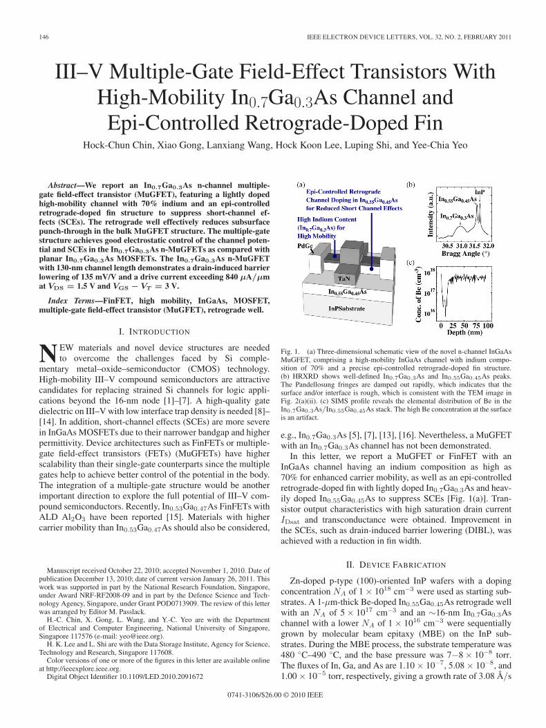
Fig. 1. (a) Three-dimensional schematic view of the novel n-channel InGaAsMuGFET, comprising a high-mobility InGaAs channel with indium compo-sition of 70% and a precise epi-controlled retrograde-doped fin structure.(b) HRXRD shows well-defined In0.7Ga0.3As and In0.55Ga0.45As peaks.The Pandellosung fringes are damped out rapidly, which indicates that thesurface and/or interface is rough, which is consistent with the TEM image inFig. 2(a)(ii). (c) SIMS profile reveals the elemental distribution of Be in theIn0.7Ga0.3As/In0.55Ga0.45As stack. The high Be concentration at the surfaceis an artifact.
e.g., In0.7Ga0.3As [5], [7], [13], [16]. Nevertheless, a MuGFETwith an In0.7Ga0.3As channel has not been demonstrated.
In this letter, we report a MuGFET or FinFET with anInGaAs channel having an indium composition as high as70% for enhanced carrier mobility, as well as an epi-controlledretrograde-doped fin with lightly doped In0.7Ga0.3As and heav-ily doped In0.55Ga0.45As to suppress SCEs [Fig. 1(a)]. Tran-sistor output characteristics with high saturation drain currentIDsat and transconductance were obtained. Improvement inthe SCEs, such as drain-induced barrier lowering (DIBL), wasachieved with a reduction in fin width.
II. DEVICE FABRICATION
Zn-doped p-type (100)-oriented InP wafers with a dopingconcentration NA of 1 × 1018 cm−3 were used as starting sub-strates. A 1-μm-thick Be-doped In0.55Ga0.45As retrograde wellwith an NA of 5 × 1017 cm−3 and an ∼16-nm In0.7Ga0.3Aschannel with a lower NA of 1 × 1016 cm−3 were sequentiallygrown by molecular beam epitaxy (MBE) on the InP sub-strates. During the MBE process, the substrate temperature was480 ◦C–490 ◦C, and the base pressure was 7−8 × 10⁻⁸ torr.The fluxes of In, Ga, and As are 1.10 × 10⁻⁷, 5.08 × 10⁻⁸, and1.00 × 10−5 torr, respectively, giving a growth rate of 3.08 Å/s
0741-3106/$26.00 © 2010 IEEE
CHIN et al.: III–V MULTIPLE-GATE FIELD-EFFECT TRANSISTORS 147
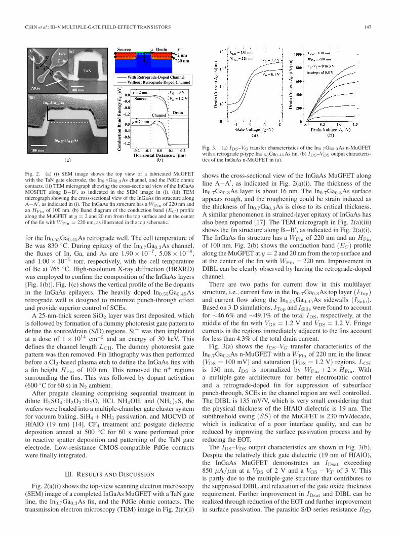
Fig. 2. (a) (i) SEM image shows the top view of a fabricated MuGFETwith the TaN gate electrode, the In0.7Ga0.3As channel, and the PdGe ohmiccontacts. (ii) TEM micrograph showing the cross-sectional view of the InGaAsMOSFET along B−B′, as indicated in the SEM image in (i). (iii) TEMmicrograph showing the cross-sectional view of the InGaAs fin structure alongA−A′, as indicated in (i). The InGaAs fin structure has a WFin of 220 nm andan HFin of 100 nm. (b) Band diagram of the conduction band (EC) profilealong the MuGFET at y = 2 and 20 nm from the top surface and at the centerof the fin with WFin = 220 nm, as illustrated in the top schematic.
for the In0.55Ga0.45As retrograde well. The cell temperature ofBe was 830 ◦C. During epitaxy of the In0.7Ga0.3As channel,the fluxes of In, Ga, and As are 1.90 × 10⁻⁷, 5.08 × 10⁻⁸,and 1.00 × 10⁻⁵ torr, respectively, with the cell temperatureof Be at 765 ◦C. High-resolution X-ray diffraction (HRXRD)was employed to confirm the composition of the InGaAs layers[Fig. 1(b)]. Fig. 1(c) shows the vertical profile of the Be dopantsin the InGaAs epilayers. The heavily doped In0.55Ga0.45Asretrograde well is designed to minimize punch-through effectand provide superior control of SCEs.
A 25-nm-thick screen SiO2 layer was first deposited, whichis followed by formation of a dummy photoresist gate pattern todefine the source/drain (S/D) regions. Si+ was then implantedat a dose of 1 × 1014 cm−2 and an energy of 30 keV. Thisdefines the channel length LCH. The dummy photoresist gatepattern was then removed. Fin lithography was then performedbefore a Cl2-based plasma etch to define the InGaAs fins witha fin height HFin of 100 nm. This removed the n+ regionssurrounding the fins. This was followed by dopant activation(600 ◦C for 60 s) in N2 ambient.
After pregate cleaning comprising sequential treatment indilute H2SO4 :H2O2 :H2O, HCl, NH4OH, and (NH4)2S, thewafers were loaded into a multiple-chamber gate cluster systemfor vacuum baking, SiH4 + NH3 passivation, and MOCVD ofHfAlO (19 nm) [14]. CF4 treatment and postgate dielectricdeposition anneal at 500 ◦C for 60 s were performed priorto reactive sputter deposition and patterning of the TaN gateelectrode. Low-resistance CMOS-compatible PdGe contactswere finally integrated.
III. RESULTS AND DISCUSSION
Fig. 2(a)(i) shows the top-view scanning electron microscopy(SEM) image of a completed InGaAs MuGFET with a TaN gateline, the In0.7Ga0.3As fin, and the PdGe ohmic contacts. Thetransmission electron microscopy (TEM) image in Fig. 2(a)(ii)
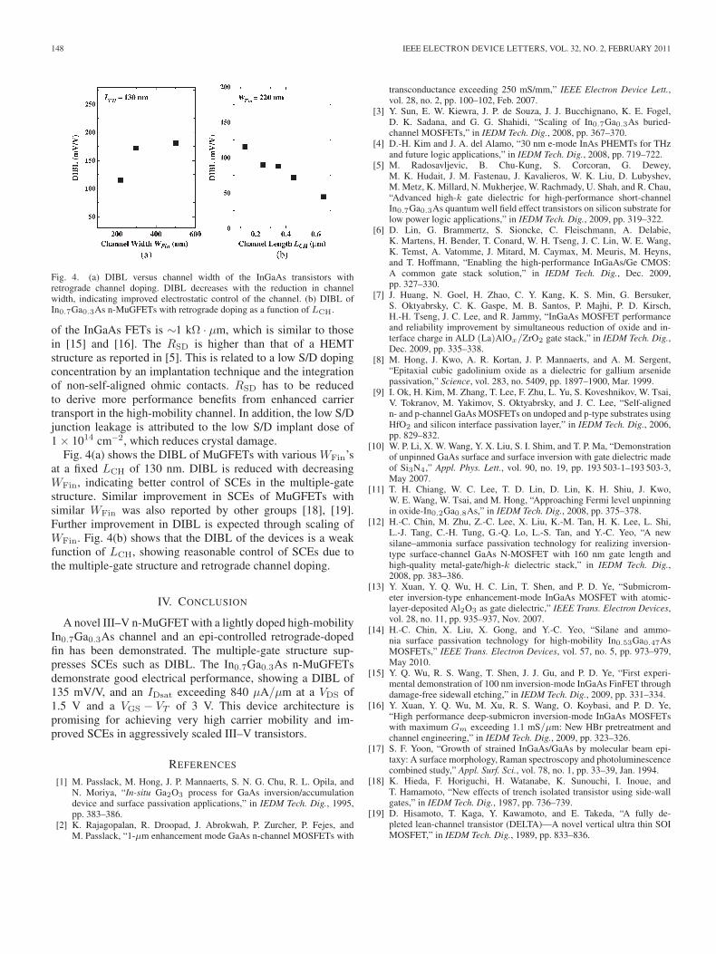
Fig. 3. (a) IDS–VG transfer characteristics of the In0.7Ga0.3As n-MuGFETwith a retrograde p-type In0.55Ga0.45As fin. (b) IDS–VDS output characteris-tics of the InGaAs n-MuGFET in (a).
shows the cross-sectional view of the InGaAs MuGFET alongline A−A′, as indicated in Fig. 2(a)(i). The thickness of theIn0.7Ga0.3As layer is about 16 nm. The In0.7Ga0.3As surfaceappears rough, and the roughening could be strain induced asthe thickness of In0.7Ga0.3As is close to its critical thickness.A similar phenomenon in strained-layer epitaxy of InGaAs hasalso been reported [17]. The TEM micrograph in Fig. 2(a)(iii)shows the fin structure along B−B′, as indicated in Fig. 2(a)(i).The InGaAs fin structure has a WFin of 220 nm and an HFin
of 100 nm. Fig. 2(b) shows the conduction band (EC) profilealong the MuGFET at y = 2 and 20 nm from the top surface andat the center of the fin with WFin = 220 nm. Improvement inDIBL can be clearly observed by having the retrograde-dopedchannel.
There are two paths for current flow in this multilayerstructure, i.e., current flow in the In0.7Ga0.3As top layer (ITop)and current flow along the In0.55Ga0.45As sidewalls (ISide).Based on 3-D simulations, ITop and ISide were found to accountfor ∼46.6% and ∼49.1% of the total IDS, respectively, at themiddle of the fin with VGS = 1.2 V and VDS = 1.2 V. Fringecurrents in the regions immediately adjacent to the fins accountfor less than 4.3% of the total drain current.
Fig. 3(a) shows the IDS–VG transfer characteristics of theIn0.7Ga0.3As n-MuGFET with a WFin of 220 nm in the linear(VDS = 100 mV) and saturation (VDS = 1.2 V) regions. LCH
is 130 nm. IDS is normalized by WFin + 2 ×HFin. Witha multiple-gate architecture for better electrostatic controland a retrograde-doped fin for suppression of subsurfacepunch-through, SCEs in the channel region are well controlled.The DIBL is 135 mV/V, which is very small considering thatthe physical thickness of the HfAlO dielectric is 19 nm. Thesubthreshold swing (SS) of the MuGFET is 230 mV/decade,which is indicative of a poor interface quality, and can bereduced by improving the surface passivation process and byreducing the EOT.
The IDS–VDS output characteristics are shown in Fig. 3(b).Despite the relatively thick gate dielectric (19 nm of HfAlO),the InGaAs MuGFET demonstrates an IDsat exceeding850 μA/μm at a VDS of 2 V and a VGS − VT of 3 V. Thisis partly due to the multiple-gate structure that contributes tothe suppressed DIBL and relaxation of the gate oxide thicknessrequirement. Further improvement in IDsat and DIBL can berealized through reduction of the EOT and further improvementin surface passivation. The parasitic S/D series resistance RSD
148 IEEE ELECTRON DEVICE LETTERS, VOL. 32, NO. 2, FEBRUARY 2011
Fig. 4. (a) DIBL versus channel width of the InGaAs transistors withretrograde channel doping. DIBL decreases with the reduction in channelwidth, indicating improved electrostatic control of the channel. (b) DIBL ofIn0.7Ga0.3As n-MuGFETs with retrograde doping as a function of LCH.
of the InGaAs FETs is ∼1 kΩ · μm, which is similar to thosein [15] and [16]. The RSD is higher than that of a HEMTstructure as reported in [5]. This is related to a low S/D dopingconcentration by an implantation technique and the integrationof non-self-aligned ohmic contacts. RSD has to be reducedto derive more performance benefits from enhanced carriertransport in the high-mobility channel. In addition, the low S/Djunction leakage is attributed to the low S/D implant dose of1 × 1014 cm−2, which reduces crystal damage.
Fig. 4(a) shows the DIBL of MuGFETs with various WFin’sat a fixed LCH of 130 nm. DIBL is reduced with decreasingWFin, indicating better control of SCEs in the multiple-gatestructure. Similar improvement in SCEs of MuGFETs withsimilar WFin was also reported by other groups [18], [19].Further improvement in DIBL is expected through scaling ofWFin. Fig. 4(b) shows that the DIBL of the devices is a weakfunction of LCH, showing reasonable control of SCEs due tothe multiple-gate structure and retrograde channel doping.
IV. CONCLUSION
A novel III–V n-MuGFET with a lightly doped high-mobilityIn0.7Ga0.3As channel and an epi-controlled retrograde-dopedfin has been demonstrated. The multiple-gate structure sup-presses SCEs such as DIBL. The In0.7Ga0.3As n-MuGFETsdemonstrate good electrical performance, showing a DIBL of135 mV/V, and an IDsat exceeding 840 μA/μm at a VDS of1.5 V and a VGS − VT of 3 V. This device architecture ispromising for achieving very high carrier mobility and im-proved SCEs in aggressively scaled III–V transistors.
REFERENCES
[1] M. Passlack, M. Hong, J. P. Mannaerts, S. N. G. Chu, R. L. Opila, andN. Moriya, “In-situ Ga2O3 process for GaAs inversion/accumulationdevice and surface passivation applications,” in IEDM Tech. Dig., 1995,pp. 383–386.
[2] K. Rajagopalan, R. Droopad, J. Abrokwah, P. Zurcher, P. Fejes, andM. Passlack, “1-μm enhancement mode GaAs n-channel MOSFETs with
transconductance exceeding 250 mS/mm,” IEEE Electron Device Lett.,vol. 28, no. 2, pp. 100–102, Feb. 2007.
[3] Y. Sun, E. W. Kiewra, J. P. de Souza, J. J. Bucchignano, K. E. Fogel,D. K. Sadana, and G. G. Shahidi, “Scaling of In0.7Ga0.3As buried-channel MOSFETs,” in IEDM Tech. Dig., 2008, pp. 367–370.
[4] D.-H. Kim and J. A. del Alamo, “30 nm e-mode InAs PHEMTs for THzand future logic applications,” in IEDM Tech. Dig., 2008, pp. 719–722.
[5] M. Radosavljevic, B. Chu-Kung, S. Corcoran, G. Dewey,M. K. Hudait, J. M. Fastenau, J. Kavalieros, W. K. Liu, D. Lubyshev,M. Metz, K. Millard, N. Mukherjee, W. Rachmady, U. Shah, and R. Chau,“Advanced high-k gate dielectric for high-performance short-channelIn0.7Ga0.3As quantum well field effect transistors on silicon substrate forlow power logic applications,” in IEDM Tech. Dig., 2009, pp. 319–322.
[6] D. Lin, G. Brammertz, S. Sioncke, C. Fleischmann, A. Delabie,K. Martens, H. Bender, T. Conard, W. H. Tseng, J. C. Lin, W. E. Wang,K. Temst, A. Vatomme, J. Mitard, M. Caymax, M. Meuris, M. Heyns,and T. Hoffmann, “Enabling the high-performance InGaAs/Ge CMOS:A common gate stack solution,” in IEDM Tech. Dig., Dec. 2009,pp. 327–330.
[7] J. Huang, N. Goel, H. Zhao, C. Y. Kang, K. S. Min, G. Bersuker,S. Oktyabrsky, C. K. Gaspe, M. B. Santos, P. Majhi, P. D. Kirsch,H.-H. Tseng, J. C. Lee, and R. Jammy, “InGaAs MOSFET performanceand reliability improvement by simultaneous reduction of oxide and in-terface charge in ALD (La)AlOx/ZrO2 gate stack,” in IEDM Tech. Dig.,Dec. 2009, pp. 335–338.
[8] M. Hong, J. Kwo, A. R. Kortan, J. P. Mannaerts, and A. M. Sergent,“Epitaxial cubic gadolinium oxide as a dielectric for gallium arsenidepassivation,” Science, vol. 283, no. 5409, pp. 1897–1900, Mar. 1999.
[9] I. Ok, H. Kim, M. Zhang, T. Lee, F. Zhu, L. Yu, S. Koveshnikov, W. Tsai,V. Tokranov, M. Yakimov, S. Oktyabrsky, and J. C. Lee, “Self-alignedn- and p-channel GaAs MOSFETs on undoped and p-type substrates usingHfO2 and silicon interface passivation layer,” in IEDM Tech. Dig., 2006,pp. 829–832.
[10] W. P. Li, X. W. Wang, Y. X. Liu, S. I. Shim, and T. P. Ma, “Demonstrationof unpinned GaAs surface and surface inversion with gate dielectric madeof Si3N4,” Appl. Phys. Lett., vol. 90, no. 19, pp. 193 503-1–193 503-3,May 2007.
[11] T. H. Chiang, W. C. Lee, T. D. Lin, D. Lin, K. H. Shiu, J. Kwo,W. E. Wang, W. Tsai, and M. Hong, “Approaching Fermi level unpinningin oxide-In0.2Ga0.8As,” in IEDM Tech. Dig., 2008, pp. 375–378.
[12] H.-C. Chin, M. Zhu, Z.-C. Lee, X. Liu, K.-M. Tan, H. K. Lee, L. Shi,L.-J. Tang, C.-H. Tung, G.-Q. Lo, L.-S. Tan, and Y.-C. Yeo, “A newsilane–ammonia surface passivation technology for realizing inversion-type surface-channel GaAs N-MOSFET with 160 nm gate length andhigh-quality metal-gate/high-k dielectric stack,” in IEDM Tech. Dig.,2008, pp. 383–386.
[13] Y. Xuan, Y. Q. Wu, H. C. Lin, T. Shen, and P. D. Ye, “Submicrom-eter inversion-type enhancement-mode InGaAs MOSFET with atomic-layer-deposited Al2O3 as gate dielectric,” IEEE Trans. Electron Devices,vol. 28, no. 11, pp. 935–937, Nov. 2007.
[14] H.-C. Chin, X. Liu, X. Gong, and Y.-C. Yeo, “Silane and ammo-nia surface passivation technology for high-mobility In0.53Ga0.47AsMOSFETs,” IEEE Trans. Electron Devices, vol. 57, no. 5, pp. 973–979,May 2010.
[15] Y. Q. Wu, R. S. Wang, T. Shen, J. J. Gu, and P. D. Ye, “First experi-mental demonstration of 100 nm inversion-mode InGaAs FinFET throughdamage-free sidewall etching,” in IEDM Tech. Dig., 2009, pp. 331–334.
[16] Y. Xuan, Y. Q. Wu, M. Xu, R. S. Wang, O. Koybasi, and P. D. Ye,“High performance deep-submicron inversion-mode InGaAs MOSFETswith maximum Gm exceeding 1.1 mS/μm: New HBr pretreatment andchannel engineering,” in IEDM Tech. Dig., 2009, pp. 323–326.
[17] S. F. Yoon, “Growth of strained InGaAs/GaAs by molecular beam epi-taxy: A surface morphology, Raman spectroscopy and photoluminescencecombined study,” Appl. Surf. Sci., vol. 78, no. 1, pp. 33–39, Jan. 1994.
[18] K. Hieda, F. Horiguchi, H. Watanabe, K. Sunouchi, I. Inoue, andT. Hamamoto, “New effects of trench isolated transistor using side-wallgates,” in IEDM Tech. Dig., 1987, pp. 736–739.
[19] D. Hisamoto, T. Kaga, Y. Kawamoto, and E. Takeda, “A fully de-pleted lean-channel transistor (DELTA)—A novel vertical ultra thin SOIMOSFET,” in IEDM Tech. Dig., 1989, pp. 833–836.