Embed Size (px)
Citation preview
Advances in Computational Sciences and Technology
ISSN 0973-6107 Volume 10, Number 10 (2017) pp. 2985-3013
© Research India Publications
http://www.ripublication.com
III-V Compound Semiconductor Laser
Heterostructures Parametric Performance Evaluation
For InGaAs/GaAs And AlGaAs/GaAs
Saima Beg1, Syed Hasan Saeed2, M.J.Siddiqui3
1Department of ECE, Integral University, Lucknow, U.P. India 2Department of ECE, Integral University, Lucknow, U.P., India
3Department of Electronics Engineering, Z.H.college of Engineering and Technology, AMU, Aligarh, U.P.
Abstract
This paper presented a detailed analysis and up-to-date performance
evaluation using the band parameters for the technologically important III–V
compound semiconductors heterostructures of InGaAs/GaAs and
AlGaAs/GaAs in terms of gain spectrum along with their wavelength variation
with respect to quantum well/barrier thickness, relaxation time and
concentration. Using the vast literature review of the consistent parameter sets
and energy transition is evaluated by applying model of solid theory for both
materials. Emphasizing the effect of strain over lattice structure band structure
calculations are performed using simulated mathematical model. The results
are evaluated by simulated model by considering the direct and indirect energy
gaps, crystal field splitting, bowing parameters, effective masses for electrons,
heavy, light, and split-off holes, Luttinger parameters, interband momentum
matrix elements, and lattice deformation at specific temperature and different
alloy-composition concentration.
INTRODUCTION
A compound semiconductor is composed of elements from two or more different
groups of the periodic table. GaN, GaAs, InP, InN, InGaN, AlGaN, AlGaAs etc.
referred as III-V semiconducting binary and ternary compounds. Many of these
compound semiconductors have electrical and optical properties. Extensive research
2986 Saima Beg, Syed Hasan Saeed, M.J.Siddiqui
is being done in the field of Semiconductor technology and the development has been
rapid in the past few years. Primary semiconductors fill the last decade were Silicon
(Si) and Group III-V materials such as Gallium Arsenide (GaAs) and Aluminium
Arsenide (AlAs). Although these materials have extensive application, they are found
limited in their usage associated with their narrow bandgap (1.1 eV for Si and 1.4 eV
for GaAs). Due to the fact that electrons can easily travel from the valence band to the
conduction band in a material with a narrow band gap, it makes these materials
unappealing for high temperature and high power applications.
In the 1970s, considerable interests were shown on group III-nitrides. But during that
time, developing low-ohmic p-type group III-nitrides failed. As technology improved
in the late 1980's such low-ohmic p-type group III-nitrides were developed reinitiating
the interest in the field.
The group III-nitrides Gallium Nitride (GaN), Aluminium Nitride (AlN) and Indium
Nitride (InN) with related alloys form an interesting class of wide band gap materials.
These materials find special usage in Optronics as well as in electronics due to the
fact that the entire spectral region from UV to red can be covered with III-N optical
devices. These materials form a continuous alloy system made up of Indium Gallium
Nitride (InGaN), Indium Aluminium Nitride (InAlN), and Aluminium Gallium
Nitride (AlGaN) whose direct optical band gaps for the hexagonal Wurtzite phase
range from 0.7 eV for InN and 3.4 eV for GaN to 6.2 eV for AlN. The band gap of
InN has been recently found out to be 0.7 eV. Previously, it has been thought to be 1.9
eV. This is not possible with III-V material system based on GaAs, AlAs, GaP, InAs
and related alloys.
Laser can cover the spectral range of wavelength range of 400 nm to 2 μm by
combining various semiconductors compound. In 1966 theoretically it was found that
the double heterostructure (DHS) can be realized by using optical confinement i.e.
wave guiding [6]. A revolutionary change in the development of semiconductor diode
lasers was introduced with the concept of double heterostructure application in the
active region of an injection laser for obtaining better electron confinement efficiency
[4], [5]. Initially most of the scientific work was unaware of the approach based on
design of a heterostructure of other band gaps and having lattice matching at better
level.
It was assumed that since III–V materials have different band gap energies hence they
may give different lattice constants.But with the finding of a stable AlGaAs alloy and
design of a lattice-matched AlGaAs–GaAs “sandwich”-like DHS practically gave a
first time moment of obtaining a low-threshold current density pulsed lasing at room
temperature. Presently laser wave-length can be selected by varying the composition
of the material mol fraction given as x, y, z.
InxAlyGa1–x–yN materials are used for the blue to green laser wavelength [16, 17].
III-V Compound Semiconductor Laser Heterostructures Parametric… 2987
InxAlyGa1-x-yP are useful for generation of laser wavelength in the range 615 nm and
750 nm for red emitting diodes. AlxGa 1-xAs1-y Py produces lasers of spectral
wavelength range in 670 nm and 890 nm. InxGa1-xAsyP1-y or In1-x-y AlxGayAs, with
GaAs provides a longer wavelength of the level 1.2 μm [18, 19]. With the InP as
substrates the InxGa1-xAs yP1-y or In 1-x-y AlxGayAs can cover the range up to 2.3μm.
Antimonide based structures can provide longer wavelengths known as salt lasers or
latest one called as quantum cascade lasers.[20]
CMOS technology is gradually dominating the electronic market in the last few
decades. Due to the CMOS technology the reduction in the transistors size of created
a typical challenge in respect of metallic connections and interconnects. Due to the
thermal compensation problem in the multilayered semiconductor transistors with
metallic links there are large challenges in higher level of miniaturization. The use of
optical links in the integrated circuits introduces a break-through in the technology
with the use active photonic material on the semiconductor wafer for obtaining high-
speed interchip and intrachip optical connection. This can provide economical
benefits in the CMOS industry with fulfilling the need of low-power consumption for
next-generation telecommunication applications.
Single semiconductor based nano wire lasers are designed using various materials in
the recent years. These lasers provide emission having spectral wavelength of range.
It belongs to ultraviolet to infrared regions due to its very wide bandgaps [1–3][21]
.III–V Active material-based nano wires in cylindrical design in the diameter of
hundreds of nanometers and with micrometers lengths are also developed which
provides efficient confinement and optical wave guide inside the gain medium on a
nanometer scale. They are also compatible on integration with optically active III–V
semiconductors with the available silicon technologies despite high mismatch of
lattice constant in between them. The array structures of nano wires are also useful in
forming micro source cavity for obtaining slow group velocity mode having high
optical energy generation capability in a given gain medium. The above benefits
cause higher demand for realization of nano photonic lasers for fulfilling the need of
coherent light micro sources for photonics application-based integrated circuits. [21]
Theoretical proofs and experimental results are available related to the semiconductor
heterostructure lasers which helped to demonstrate that III–V materials used for lasers
exhibit the property of reduction of threshold current density on decreasing the active
region thickness. The cause behind this effect is that a thicker active region needs the
high quantity of carriers injection. In the design of quantum well (QW) separate
confinement heterostructures (SCHs), a very low level of carrier injection is required.
[21]
In the last decades ultrafast acting lasers are designed which have come into existence
with higher performance in a short duration. Recently available ultrafast laser in
2988 Saima Beg, Syed Hasan Saeed, M.J.Siddiqui
practical and commercial systems are the result of combining the simplicity of
semiconductor saturable absorber mirror (SESAM) mode locked lasers to the diode-
pumped solid-state lasers (DPSSLs) in the 1990s, [3, 4] These ultrafast laser systems
are applied in the systems where expensive, power-hungry, maintenance-intensive
lasers are to be replaced. These ultrafast lasers are beneficial for many applications
related to short pulse duration related measurements with requirement of high level
resolution. They act like a ultrafast flash light to record the high-speed dynamical
process. Since in the ultrafast laser the radiation power is delivered in concentrated
form for a very short duration, hence it consists of very high peak power which is
very helpful in activating material interactions. One of its examples is “cold ablation”
in which short duration optical pulse is able to remove almost any material without
leaving large amount of residual heat in the material sample that has been considered
under a particular process. Cold ablation technique helps in high precision micro level
machining of different available and novel materials and thin films that can produce
future products at high potential. It is also helpful in latest applications in biomedical
and tissue surgery process. Temporally short duration pulses that are generated by
ultrafast lasers exhibits large optical bandwidths which can be used for high precision
measurement diagnostics applications. A current achievement in the laser is
semiconductor disk lasers (SDL) which gives higher compactness and availability at
low cost. This development is very useful for small size devices required for
metrology applications. The growth of ultrafast laser with properties of low cost and
small size SDL’s opens up the large amount of market demand for consumer products
related to the equipments used for photo detection and ranging applications in the
automotive companies[5] or natural user interface requirements found in security and
interactive applications.[22]
Ultrafast SDL’s are cheaper and gives better compactness in comparison to ultrafast
lasers hence it can be operated very efficiently in the gigahertz pulse rate related
platforms in the process involved in producing semiconductor wafer and can be
successfully added in various optical circuits of high level of complexity [8, 9].
From the previous discussions in this paper we can also say that with the
incorporation of band gap based engineering development, the spectral wavelength of
these ultrafast can be configured at high repetition rate of several tens of GHz without
any switching related unstable conditions and errors. [22]
THEORETICAL MODEL FOR GAIN SPECTRUM AND WAVELENGTH
CALCULATION:
Energy band gap of semiconductors is expressed as a function of temperature and
carrier concentration given as:
Eg (T,nc) = Eg(T)+∆Eg(nc) (1)
III-V Compound Semiconductor Laser Heterostructures Parametric… 2989
Band gap is reduced as the temperature is raised due to the change of the lattice
constant hence it can be described using the formula that has proposed in [23].
𝐸𝑔 = 𝐸(0) −𝛼 ⊝𝑃
2[ √1 + (
2𝑇
⊝𝑃)𝑃 − 1
𝑝
] (2)
𝑇 =(𝑇𝐶+𝑇𝐻)
2 (3)
Where 𝛼 : slope parameter at T→ ∞,
⊝ : average photon on,
p is the photon dispersion parameter.
Quantum levels for the conduction bands (Ec,str ) and valence bands (Eyy,str ) is
described as:
𝐸𝑥𝑥,𝑠𝑡𝑟𝑛 = 𝐸𝑥𝑥,𝑏
𝑛 + ∆𝐸𝑥𝑥,𝑠𝑡𝑟 (4)
Here xx denotes c, hh, lh. On including the influence of the barrier [24] 𝐸𝑥𝑥,𝑏𝑛 can be
defined as:
𝐸𝑥𝑥,𝑏𝑛 = 𝐸𝑥𝑥
𝑛 𝑛2(𝑛 +2
𝜋√
𝑚𝑥𝑥,𝑏 𝐸𝑥𝑥𝑛
𝑚𝑥𝑥(∆𝐸𝑥𝑥 + ∆𝐸𝑥𝑥,𝑠𝑡𝑟))−2 (5)
𝐸𝑥𝑥𝑛 =
𝜋2ℏ2𝑛2
2𝑚𝑥𝑥𝑡𝑞𝑤2
(6)
Where 𝐸𝑥𝑥𝑛 : quantum level for an infinite barrier,
n: quantum level number
𝑚𝑥𝑥,𝑏 :effective mass of the barrier.
∆𝐸𝑐 and ∆𝐸𝑣are the potential barrier heights for calculation of the conduction and
valence bands by using the electron affinity.The respective equation for barrier height
are given below in equation 7 and 8 [26]:
∆𝐸𝑐 = 𝜒𝑜𝑞𝑤 − 𝜒𝑜𝑏𝑎𝑟 (7)
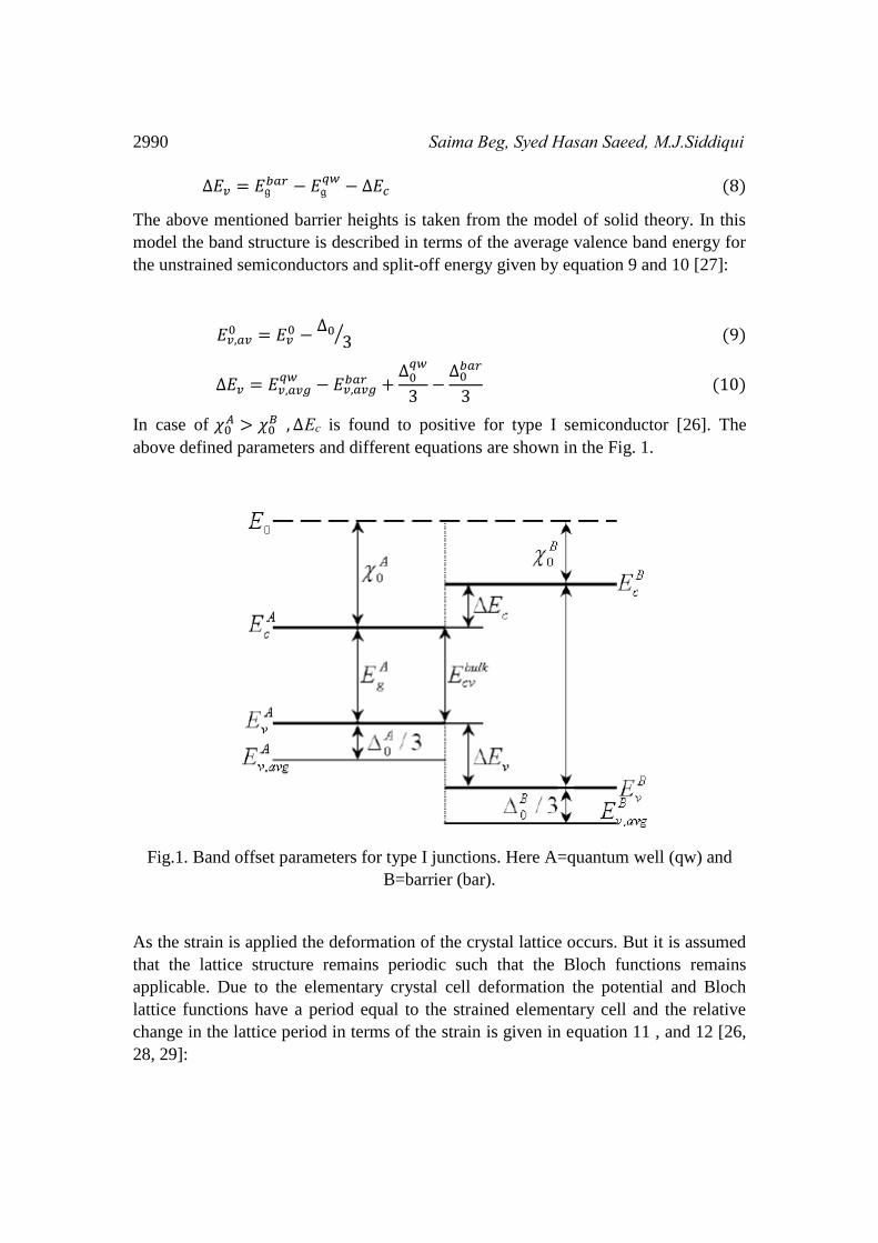
2990 Saima Beg, Syed Hasan Saeed, M.J.Siddiqui
∆𝐸𝑣 = 𝐸𝔤𝑏𝑎𝑟 − 𝐸𝔤
𝑞𝑤 − ∆𝐸𝑐 (8)
The above mentioned barrier heights is taken from the model of solid theory. In this
model the band structure is described in terms of the average valence band energy for
the unstrained semiconductors and split-off energy given by equation 9 and 10 [27]:
𝐸𝑣,𝑎𝑣0 = 𝐸𝑣
0 −∆0
3⁄ (9)
∆𝐸𝑣 = 𝐸𝑣,𝑎𝑣𝑔𝑞𝑤 − 𝐸𝑣,𝑎𝑣𝑔
𝑏𝑎𝑟 +∆0
𝑞𝑤
3−
∆0𝑏𝑎𝑟
3 (10)
In case of 𝜒0𝐴 > 𝜒0
𝐵 , ∆Ec is found to positive for type I semiconductor [26]. The
above defined parameters and different equations are shown in the Fig. 1.
Fig.1. Band offset parameters for type I junctions. Here A=quantum well (qw) and
B=barrier (bar).
As the strain is applied the deformation of the crystal lattice occurs. But it is assumed
that the lattice structure remains periodic such that the Bloch functions remains
applicable. Due to the elementary crystal cell deformation the potential and Bloch
lattice functions have a period equal to the strained elementary cell and the relative
change in the lattice period in terms of the strain is given in equation 11 , and 12 [26,
28, 29]:

III-V Compound Semiconductor Laser Heterostructures Parametric… 2991
𝜖𝑥𝑥 = 𝜖𝑦𝑦 = 𝜖𝑠𝑡𝑟 =(𝑎0 − 𝑎𝑞𝑤)
𝑎𝑤 (11)
𝑎 = 𝑎 + 𝑎𝑡 × 10−5(𝑇 − 300) (12)
The two strain components are related by the elastic stiffness constants C11and C12
as:
∈𝑧𝑧= −2𝐶12
𝐶11𝑒𝑥𝑥 (13)
𝑃∈,𝑥𝑎𝑛𝑑𝑄𝑒 are used as the additional terms as the diagonal elements of the two-band
Hamiltonian matrix expressed using equation 14 and 15 [11].
𝑃∈,𝑥 = −𝑎𝑥(∈𝑥𝑥+∈𝑦𝑦+∈𝑧𝑧) (14)
𝑄∈ = −0.5𝑏(∈𝑥𝑥+∈𝑦𝑦− 2 ∈𝑧𝑧) (15)
𝜖𝑥𝑥, 𝜖𝑦𝑦. 𝜖𝑧𝑧 𝑎𝑛𝑑 𝜖𝑠𝑡𝑟 : strain components in all directions;
𝑎𝑞𝑤𝑎𝑛𝑑 𝑎0 : lattice constants of QW and substrate;
𝑎𝑇 : Temperature expansion coefficient;
ac and av: hydrostatic deformation potentials;
bv : shear deformation potential.
Hence the effect of strain causes the following shifts in the value of ∆Eyy,str of the CB
and HHB edges at the Г point.
∆𝐸𝑐,𝑠𝑡𝑟 = 𝑃∈,𝑐 (16)
∆𝐸ℎℎ,𝑠𝑡𝑟 = −𝑃∈,𝑣 − 𝑄∈ (17)
The final energy levels positions for conduction band are Enc,str=En
c,b+Eg qw for type I
semiconductor (18) and for valence band
𝐸ℎℎ,𝑠𝑡𝑟𝑛 = 𝐸ℎℎ,𝑏
𝑛 − ∆𝐸ℎℎ,𝑠𝑡𝑟 (18)
𝐸𝑙ℎ𝑛 = 𝐸𝑙ℎ,𝑏
𝑛 − ∆𝐸𝑙ℎ,𝑠𝑡𝑟 (19)
Assuming the transitions from sub bands with the same quantum numbers
(k-selection):
𝐸𝑐−𝑦𝑦𝑛 = 𝐸𝑐,𝑠𝑡𝑟
𝑛 + 𝐸𝑦𝑦,𝑠𝑡𝑟𝑛 (20)
Depending of strain type (compressive or tensile) lowest transition will be
conduction-heavy hole (c-hh) or conduction-light hole (c-lh), respectively. Finally,
2992 Saima Beg, Syed Hasan Saeed, M.J.Siddiqui
expression for transition energy can be described as:
𝐸𝑡𝑟𝑎𝑛 = min(𝐸𝑐−ℎℎ1 , 𝐸𝑐−𝑙ℎ
1 ) (21)
And transition wavelength
𝜆(𝜇𝑚) =1.242
𝐸𝑡𝑟𝑎𝑛(𝑒𝑉) (22)
Parameters of ternary alloys TABC AxB1-xC are usually given as linear interpolation of
binary alloys with an empirical bowing parameter CABC[1]:
𝑇𝐴𝐵𝐶(𝑥) = 𝑥𝐵𝐴𝐵 + (1 − 𝑥)𝐵𝐴𝐶 − 𝑥(1 − 𝑥)𝐶𝐴𝐵𝐶 (23)
Using the transition energy equation the wavelength and spectrum gain is evaluated in
this work at different quantum well thickness and barrier thickness and discussed in
upcoming sections.
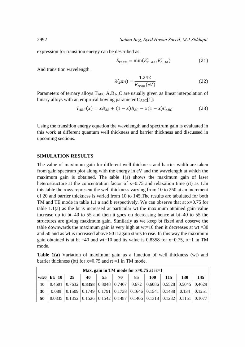
SIMULATION RESULTS
The value of maximum gain for different well thickness and barrier width are taken
from gain spectrum plot along with the energy in eV and the wavelength at which the
maximum gain is obtained. The table 1(a) shows the maximum gain of laser
heterostructure at the concentration factor of x=0.75 and relaxation time (rt) as 1.In
this table the rows represent the well thickness varying from 10 to 250 at an increment
of 20 and barrier thickness is varied from 10 to 145.The results are tabulated for both
TM and TE mode in table 1.1 a and b respectively. We can observe that at x=0.75 for
table 1.1(a) as the bt is increased at particular wt the maximum attained gain value
increase up to bt=40 to 55 and then it goes on decreasing hence at bt=40 to 55 the
structures are giving maximum gain. Similarly as we keep bt fixed and observe the
table downwards the maximum gain is very high at wt=10 then it decreases at wt =30
and 50 and as wt is increased above 50 it again starts to rise. In this way the maximum
gain obtained is at bt =40 and wt=10 and its value is 0.8358 for x=0.75, rt=1 in TM
mode.
Table 1(a) Variation of maximum gain as a function of well thickness (wt) and
barrier thickness (bt) for x=0.75 and rt =1 in TM mode.
Max. gain in TM mode for x=0.75 at rt=1
wt:0 bt: 10 25 40 55 70 85 100 115 130 145
10 0.4601 0.7632 0.8358 0.8048 0.7407 0.672 0.6086 0.5528 0.5045 0.4629
30 0.089 0.1509 0.1749 0.1791 0.1738 0.1646 0.1541 0.1438 0.134 0.1251
50 0.0835 0.1352 0.1526 0.1542 0.1487 0.1406 0.1318 0.1232 0.1151 0.1077
III-V Compound Semiconductor Laser Heterostructures Parametric… 2993
70 0.1102 0.1712 0.1898 0.1901 0.1829 0.1729 0.1623 0.152 0.1424 0.1335
90 0.143 0.214 0.2339 0.2331 0.2239 0.2119 0.1993 0.187 0.1756 0.1651
110 0.1749 0.2527 0.2731 0.2712 0.2606 0.2469 0.2327 0.2189 0.206 0.1941
130 0.2051 0.2869 0.3073 0.3044 0.2925 0.2776 0.2622 0.2472 0.2332 0.2203
150 0.2334 0.3171 0.3369 0.3331 0.3204 0.3046 0.2882 0.2724 0.2575 0.2438
170 0.2598 0.3436 0.3626 0.358 0.3446 0.3282 0.3112 0.2948 0.2792 0.2648
190 0.2836 0.3661 0.3839 0.3788 0.365 0.3482 0.3308 0.3139 0.298 0.2831
210 0.3043 0.3844 0.401 0.3953 0.3812 0.3642 0.3467 0.3297 0.3135 0.2984
230 0.3192 0.3952 0.4102 0.4042 0.3902 0.3734 0.356 0.3391 0.3231 0.308
250 0.3373 0.4102 0.4241 0.4177 0.4035 0.3867 0.3694 0.3524 0.3363 0.3212
In table 1(b) if same analysis is extracted out then it is found that as bt is increased the
maximum gain increases and it is keep on increasing up to bt =40 to 55 after that the
maximum gain is decreasing as bt further increased. Hence in both TM and TE mode
maximum gain is increasing up to bt =40 and 55 respectively. The response of
maximum gain with respect to wt is observed in table 1(b) in downward direction then
it is found that the maximum is keep on increasing as the wt is increased. The highest
gain obtained in the TE mode is 0.4241 at bt =40 and wt=250.Thus it can be
concluded from the table 1(a) and (b) that TM is giving higher maximum gain of
0.8358 than TE mode at wt =10 and bt=40.
Table 1(b) Variation of maximum gain as a function of well thickness (wt) and
barrier thickness (bt) for x=0.75 and rt=1 in TM mode.
Table 1(b)
Max. gain in TE mode for x=0.75 for rt=1
wt:0 bt: 10 25 40 55 70 85 100 115 130 145
10 0.0146 0.0266 0.0321 0.0332 0.0323 0.0304 0.0283 0.0262 0.0243 0.0226
30 0.0454 0.077 0.0893 0.0914 0.0887 0.084 0.0787 0.0734 0.0684 0.0639
50 0.0773 0.1251 0.1412 0.1426 0.1376 0.1301 0.1219 0.114 0.1065 0.0997
70 0.1103 0.1714 0.19 0.1903 0.183 0.173 0.1624 0.1521 0.1425 0.1336
90 0.1432 0.2142 0.2342 0.2334 0.2242 0.2122 0.1995 0.1873 0.1758 0.1653
110 0.1752 0.253 0.2735 0.2716 0.2609 0.2473 0.233 0.2192 0.2063 0.1944
130 0.2055 0.2874 0.3078 0.3049 0.293 0.2781 0.2626 0.2477 0.2336 0.2207
150 0.2339 0.3178 0.3376 0.3338 0.3211 0.3052 0.2888 0.273 0.2581 0.2443
170 0.2608 0.3449 0.3639 0.3593 0.3459 0.3294 0.3124 0.2958 0.2803 0.2658
190 0.2843 0.367 0.3849 0.3797 0.3658 0.349 0.3316 0.3147 0.2987 0.2838
2994 Saima Beg, Syed Hasan Saeed, M.J.Siddiqui
210 0.3054 0.3857 0.4023 0.3966 0.3825 0.3655 0.3479 0.3308 0.3146 0.2994
230 0.3201 0.3963 0.4114 0.4054 0.3913 0.3745 0.3571 0.3401 0.324 0.3089
250 0.3378 0.4108 0.4246 0.4182 0.4041 0.3872 0.3699 0.3529 0.3367 0.3216
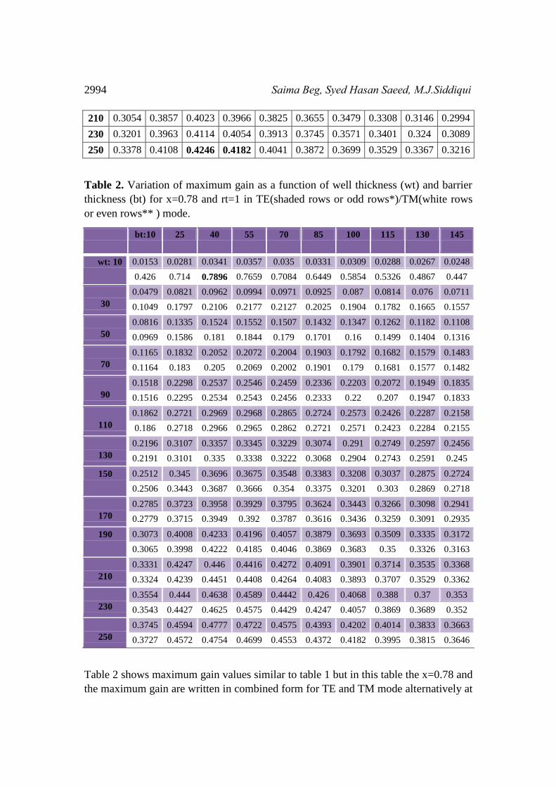
Table 2. Variation of maximum gain as a function of well thickness (wt) and barrier
thickness (bt) for x=0.78 and rt=1 in TE(shaded rows or odd rows*)/TM(white rows
or even rows** ) mode.
bt:10 25 40 55 70 85 100 115 130 145
wt: 10 0.0153 0.0281 0.0341 0.0357 0.035 0.0331 0.0309 0.0288 0.0267 0.0248
0.426 0.714 0.7896 0.7659 0.7084 0.6449 0.5854 0.5326 0.4867 0.447
30
0.0479 0.0821 0.0962 0.0994 0.0971 0.0925 0.087 0.0814 0.076 0.0711
0.1049 0.1797 0.2106 0.2177 0.2127 0.2025 0.1904 0.1782 0.1665 0.1557
50
0.0816 0.1335 0.1524 0.1552 0.1507 0.1432 0.1347 0.1262 0.1182 0.1108
0.0969 0.1586 0.181 0.1844 0.179 0.1701 0.16 0.1499 0.1404 0.1316
70
0.1165 0.1832 0.2052 0.2072 0.2004 0.1903 0.1792 0.1682 0.1579 0.1483
0.1164 0.183 0.205 0.2069 0.2002 0.1901 0.179 0.1681 0.1577 0.1482
90
0.1518 0.2298 0.2537 0.2546 0.2459 0.2336 0.2203 0.2072 0.1949 0.1835
0.1516 0.2295 0.2534 0.2543 0.2456 0.2333 0.22 0.207 0.1947 0.1833
110
0.1862 0.2721 0.2969 0.2968 0.2865 0.2724 0.2573 0.2426 0.2287 0.2158
0.186 0.2718 0.2966 0.2965 0.2862 0.2721 0.2571 0.2423 0.2284 0.2155
130
0.2196 0.3107 0.3357 0.3345 0.3229 0.3074 0.291 0.2749 0.2597 0.2456
0.2191 0.3101 0.335 0.3338 0.3222 0.3068 0.2904 0.2743 0.2591 0.245
150 0.2512 0.345 0.3696 0.3675 0.3548 0.3383 0.3208 0.3037 0.2875 0.2724
0.2506 0.3443 0.3687 0.3666 0.354 0.3375 0.3201 0.303 0.2869 0.2718
170
0.2785 0.3723 0.3958 0.3929 0.3795 0.3624 0.3443 0.3266 0.3098 0.2941
0.2779 0.3715 0.3949 0.392 0.3787 0.3616 0.3436 0.3259 0.3091 0.2935
190 0.3073 0.4008 0.4233 0.4196 0.4057 0.3879 0.3693 0.3509 0.3335 0.3172
0.3065 0.3998 0.4222 0.4185 0.4046 0.3869 0.3683 0.35 0.3326 0.3163
210
0.3331 0.4247 0.446 0.4416 0.4272 0.4091 0.3901 0.3714 0.3535 0.3368
0.3324 0.4239 0.4451 0.4408 0.4264 0.4083 0.3893 0.3707 0.3529 0.3362
230
0.3554 0.444 0.4638 0.4589 0.4442 0.426 0.4068 0.388 0.37 0.353
0.3543 0.4427 0.4625 0.4575 0.4429 0.4247 0.4057 0.3869 0.3689 0.352
250
0.3745 0.4594 0.4777 0.4722 0.4575 0.4393 0.4202 0.4014 0.3833 0.3663
0.3727 0.4572 0.4754 0.4699 0.4553 0.4372 0.4182 0.3995 0.3815 0.3646
Table 2 shows maximum gain values similar to table 1 but in this table the x=0.78 and
the maximum gain are written in combined form for TE and TM mode alternatively at
III-V Compound Semiconductor Laser Heterostructures Parametric… 2995
each common well thickness value the while colored rows are for TE mode and
shaded rows are for TM mode. It is observed that the maximum gain again follows the
same trend it increases as bt is increased to 55 in TE mode and 40, 55 or 70 for TM
mode thereafter the maximum is decreasing as bt increases. Again the maximum gain
obtained is 0.7896 in TM mode at bt 40 and wt=10 while in TE mode maximum gain
is 0.4699 at bt=55 and wt=250.Again in both modes maximum gain is found to be
increasing as wt is increased as bt is kept constant but in TM mode the maximum gain
is significantly high at wt =10 and then it reduces for wt= 30 and 50 and then the
maximum gain is increasing.
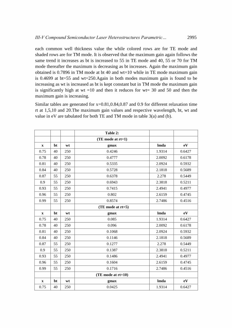
Similar tables are generated for x=0.81,0.84,0.87 and 0.9 for different relaxation time
rt at 1,5,10 and 20.The maximum gain values and respective wavelength, bt, wt and
value in eV are tabulated for both TE and TM mode in table 3(a) and (b).
Table 2:
(TE mode at rt=1)
x bt wt gmax lmda eV
0.75 40 250 0.4246 1.9314 0.6427
0.78 40 250 0.4777 2.0092 0.6178
0.81 40 250 0.5335 2.0924 0.5932
0.84 40 250 0.5728 2.1818 0.5689
0.87 55 250 0.6378 2.278 0.5449
0.9 55 250 0.6943 2.3818 0.5211
0.93 55 250 0.7415 2.4941 0.4977
0.96 55 250 0.802 2.6159 0.4745
0.99 55 250 0.8574 2.7486 0.4516
(TE mode at rt=5)
x bt wt gmax lmda eV
0.75 40 250 0.085 1.9314 0.6427
0.78 40 250 0.096 2.0092 0.6178
0.81 40 250 0.1068 2.0924 0.5932
0.84 40 250 0.1146 2.1818 0.5689
0.87 55 250 0.1277 2.278 0.5449
0.9 55 250 0.1387 2.3818 0.5211
0.93 55 250 0.1486 2.4941 0.4977
0.96 55 250 0.1604 2.6159 0.4745
0.99 55 250 0.1716 2.7486 0.4516
(TE mode at rt=10)
x bt wt gmax lmda eV
0.75 40 250 0.0425 1.9314 0.6427
2996 Saima Beg, Syed Hasan Saeed, M.J.Siddiqui
0.78 40 250 0.0483 2.0092 0.6178
0.81 40 250 0.0534 2.0924 0.5932
0.84 40 250 0.0571 2.1818 0.5689
0.87 55 250 0.064 2.278 0.5449
0.9 55 250 0.0694 2.3818 0.5211
0.93 55 250 0.0743 2.4941 0.4977
0.96 55 250 0.0802 2.6159 0.4745
0.99 55 250 0.0858 2.7486 0.4516
(TE mode at rt=20)
x bt wt gmax lmda eV
0.75 40 250 0.0214 1.9314 0.6427
0.78 40 250 0.0237 2.0092 0.6178
0.81 40 250 0.0267 2.0924 0.5932
0.84 40 250 0.0285 2.1818 0.5689
0.87 55 250 0.0319 2.278 0.5449
0.9 55 250 0.0346 2.3818 0.5211
0.93 55 250 0.037 2.4941 0.4977
0.96 55 250 0.0399 2.6159 0.4745
0.99 55 250 0.0429 2.7486 0.4516
(TM mode at rt=1)
x bt wt gmax lamda eV
0.75 40 10 0.8358 1.3511 0.9187
0.78 40 10 0.7896 1.3878 0.8944
0.81 40 10 0.8622 1.4082 0.8814
0.84 40 10 0.9909 1.4479 0.8572
0.87 40 50 1.3512 1.545 0.8033
0.9 40 50 2.7015 1.5821 0.7845
0.93 40 50 2.6587 1.6204 0.766
0.96 40 70 3.4048 1.7133 0.7245
0.99 40 50 3.6839 1.679 0.7393
(TM mode at rt=5)
x bt wt gmax lamda eV
0.75 40 10 0.1672 1.3511 0.9187
0.78 40 10 0.1579 1.3878 0.8944
0.81 40 10 0.1725 1.4082 0.8814
0.84 40 10 0.1992 1.4479 0.8572
0.87 40 50 0.2702 1.545 0.8033
0.9 40 50 0.5408 1.5821 0.7845
0.93 40 50 0.532 1.6204 0.766
III-V Compound Semiconductor Laser Heterostructures Parametric… 2997
0.96 40 70 0.6814 1.7133 0.7245
0.99 40 50 0.7368 1.679 0.7393
(TM mode at rt=10)
x bt wt gmax lamda eV
0.75 40 10 0.0836 1.3511 0.9187
0.78 40 10 0.079 1.3878 0.8944
0.81 40 10 0.0863 1.4082 0.8814
0.84 40 10 0.0996 1.4479 0.8572
0.87 40 50 0.1351 1.545 0.8033
0.9 40 50 0.2703 1.5821 0.7845
0.93 40 50 0.2658 1.6204 0.766
0.96 40 70 0.3406 1.7133 0.7245
0.99 40 50 0.3683 1.679 0.7393
(TM mode at rt=20)
x bt wt gmax lamda eV
0.75 40 10 0.0418 1.3511 0.9187
0.78 40 10 0.0395 1.3878 0.8944
0.81 40 10 0.0431 1.4082 0.8814
0.84 40 10 0.0498 1.4479 0.8572
0.87 40 50 0.0676 1.545 0.8033
0.9 40 50 0.1352 1.5821 0.7845
0.93 40 50 0.1329 1.6204 0.766
0.96 40 70 0.1703 1.7133 0.7245
0.99 40 50 0.1841 1.679 0.7393
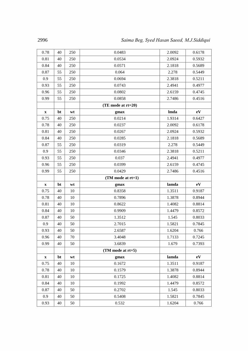
After gathering all the results for the AlGaAs/GaAs the variations in the values of
gain, energy and wavelength for both TE and TM mode with respect to barrier
thickness, well thickness, concentration, relaxation time are observed .Fig 2 (a) shows
the variation of maximum gain with respect to barrier thickness at different
concentration x. In this case wt and rt is kept constant wt=250 and rt=1 is chosen for
this plot because the AlGaAs hetero structure provided maximum gain rt=1 and
wt=250 in TE mode as referred to table 2. Here it can be observed that barrier
thickness is varying from 10 to 150 and gain initially rises and attains maximum value
at bt =40 for x=0.75 and it reduces gradually. It can also be observed that as the
concentration x is enhanced from 0.75 to 0.99 gain is increases. Similarly fig 2 b
represents the gain vs. barrier thickness for TM mode. It can be observed that at lower
concentration x=0.75 there is no significant change in the gain but as the
concentration increases gain significantly uprises and it shows its peak value at bt =40
or 50. After bt=50 the gain again goes on decreasing in this case the maximum gain is
obtained at 3.689 in TM mode at bt=40 for wt =50 while for the same scenario max
2998 Saima Beg, Syed Hasan Saeed, M.J.Siddiqui
gain is 0.8574 in TE mode at wt=250 and bt=55.
Figure 2(a): Max. Gain vs. Barrier
Thickness at different concentration x in
TE mode.
Figure 2(b): Max. Gain vs. Barrier
Thickness at different concentration x in TM
mode.
For these values of maximum gain the respective wavelength and energy in eV is
obtained. In the case of TE mode wavelength is 2.4786 and energy is 0.4516 eV for
bt=55, wt=250, x=0.99 and max gain is 0.8574 at rt=1 while in TM mode lambda
=1.679 and energy =0.7393eV for bt=40 wt=50, x=0.99 and rt=1 with gain 3.6839.
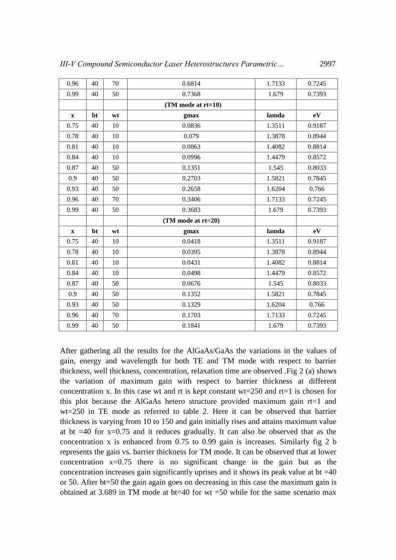
Plots to demonstrate the variations in the values of energy for both TE and TM mode
with respect to barrier thickness, well thickness concentration and relaxation time are
also shown. In Fig 2 (c and d) the value of energy (eV) with respect to barrier
thickness at different concentration x. In this case wt=250 and rt=1 with similar cause
as in figure 2(a and b). Here it can be observed as barrier thickness varied from 10 to
150 and energy is kept constant irrespective to bt. But it is observed that as the
concentration x is enhanced from 0.75 to 0.99 energy decreases. Similarly fig 2 (d)
represents the energy vs. barrier thickness for TM mode. It can be observed that at
higher concentration x=0.99 the energy is lowest that is 0.65 ev and it is kept constant
irrespective to bt. As the concentration is further enhanced there is a significant rise in
energy and as the concentration further decreased from 0.99 to 0.75 the energy
increased from 0.65 to 0.85.
0 50 100 150
0.4
0.5
0.6
0.7
0.8
0.9
1
Barrier thickness
Gain
rt=1 and wt=250 for TE mode
x=0.75
x=0.81
x=0.87
x=0.93
x=0.99
0 50 100 1500
0.5
1
1.5
2
2.5
3
3.5
4
Barrier thickness
Gain
rt=1 and wt=50 for TM mode
x=0.75
x=0.81
x=0.87
x=0.93
x=0.99
III-V Compound Semiconductor Laser Heterostructures Parametric… 2999
Figure 2(c): Energy(eV) vs. Barrier
Thickness at different concentration x in
TE mode.
Figure 2(d): Energy(eV) vs. Barrier
Thickness at different concentration x in
TM mode.
Fig 2 (e and f) shows the value of wavelength with respect to barrier thickness at
different concentration x. In this case wt=250 and rt=1 with similar cause as in figure
2(a and b). Here it can be observed as barrier thickness varied from 10 to 150 and
wavelength is kept constant irrespective to bt. But it is observed that as the
concentration x is enhanced from 0.75 to 0.99 energy decreases. Similarly fig 2 (b)
represents the wavelength vs. barrier thickness for TM mode. It can be observed that
at higher concentration x=0.99 the wavelength is lowest that is 1.5 and it is kept
constant irrespective to bt. As the concentration is further decreased there is a
significant rise in wavelength and as the concentration gradually decreased from 0.99
to 0.75 the wavelength increased from 1.5 to 1.9314.
0 50 100 1500.45
0.5
0.55
0.6
0.65
Barrier thickness
Energ
y (
eV
)
rt=1 and wt=250 for TE mode
x=0.75
x=0.81
x=0.87
x=0.93
x=0.99
0 50 100 150
0.65
0.7
0.75
0.8
0.85
Barrier thickness
Energ
y (
eV
)
rt=1 and wt=50 for TM mode
x=0.75
x=0.81
x=0.87
x=0.93
x=0.99
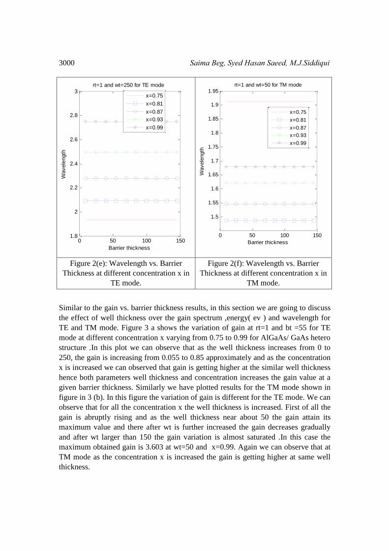
3000 Saima Beg, Syed Hasan Saeed, M.J.Siddiqui
Figure 2(e): Wavelength vs. Barrier
Thickness at different concentration x in
TE mode.
Figure 2(f): Wavelength vs. Barrier
Thickness at different concentration x in
TM mode.
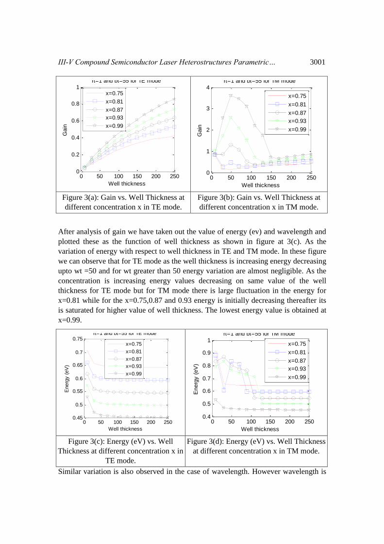
Similar to the gain vs. barrier thickness results, in this section we are going to discuss
the effect of well thickness over the gain spectrum ,energy( ev ) and wavelength for
TE and TM mode. Figure 3 a shows the variation of gain at rt=1 and bt =55 for TE
mode at different concentration x varying from 0.75 to 0.99 for AlGaAs/ GaAs hetero
structure .In this plot we can observe that as the well thickness increases from 0 to
250, the gain is increasing from 0.055 to 0.85 approximately and as the concentration
x is increased we can observed that gain is getting higher at the similar well thickness
hence both parameters well thickness and concentration increases the gain value at a
given barrier thickness. Similarly we have plotted results for the TM mode shown in
figure in 3 (b). In this figure the variation of gain is different for the TE mode. We can
observe that for all the concentration x the well thickness is increased. First of all the
gain is abruptly rising and as the well thickness near about 50 the gain attain its
maximum value and there after wt is further increased the gain decreases gradually
and after wt larger than 150 the gain variation is almost saturated .In this case the
maximum obtained gain is 3.603 at wt=50 and x=0.99. Again we can observe that at
TM mode as the concentration x is increased the gain is getting higher at same well
thickness.
0 50 100 1501.8
2
2.2
2.4
2.6
2.8
3
Barrier thickness
Wavele
ngth
rt=1 and wt=250 for TE mode
x=0.75
x=0.81
x=0.87
x=0.93
x=0.99
0 50 100 150
1.5
1.55
1.6
1.65
1.7
1.75
1.8
1.85
1.9
1.95
Barrier thickness
Wavele
ngth
rt=1 and wt=50 for TM mode
x=0.75
x=0.81
x=0.87
x=0.93
x=0.99
III-V Compound Semiconductor Laser Heterostructures Parametric… 3001
Figure 3(a): Gain vs. Well Thickness at
different concentration x in TE mode.
Figure 3(b): Gain vs. Well Thickness at
different concentration x in TM mode.
After analysis of gain we have taken out the value of energy (ev) and wavelength and
plotted these as the function of well thickness as shown in figure at 3(c). As the
variation of energy with respect to well thickness in TE and TM mode. In these figure
we can observe that for TE mode as the well thickness is increasing energy decreasing
upto wt =50 and for wt greater than 50 energy variation are almost negligible. As the
concentration is increasing energy values decreasing on same value of the well
thickness for TE mode but for TM mode there is large fluctuation in the energy for
x=0.81 while for the x=0.75,0.87 and 0.93 energy is initially decreasing thereafter its
is saturated for higher value of well thickness. The lowest energy value is obtained at
x=0.99.
Figure 3(c): Energy (eV) vs. Well
Thickness at different concentration x in
TE mode.
Figure 3(d): Energy (eV) vs. Well Thickness
at different concentration x in TM mode.
Similar variation is also observed in the case of wavelength. However wavelength is
0 50 100 150 200 2500
0.2
0.4
0.6
0.8
1
Well thickness
Gain
rt=1 and bt=55 for TE mode
x=0.75
x=0.81
x=0.87
x=0.93
x=0.99
0 50 100 150 200 2500
1
2
3
4
Well thickness
Gain
rt=1 and bt=55 for TM mode
x=0.75
x=0.81
x=0.87
x=0.93
x=0.99
0 50 100 150 200 2500.45
0.5
0.55
0.6
0.65
0.7
0.75
Well thickness
Energ
y (
eV
)
rt=1 and bt=55 for TE mode
x=0.75
x=0.81
x=0.87
x=0.93
x=0.99
0 50 100 150 200 2500.4
0.5
0.6
0.7
0.8
0.9
1
Well thickness
Energ
y (
eV
)
rt=1 and bt=55 for TM mode
x=0.75
x=0.81
x=0.87
x=0.93
x=0.99
3002 Saima Beg, Syed Hasan Saeed, M.J.Siddiqui
initially increasing with respect to well thickness thereafter as wt is getting higher wt
is getting consistent. The maximum wavelength obtained here is 2.73 approximately
at x= 0.99 for both TE & TM mode at rt=1 and bt=55.
Figure 3(e): Wavelength vs. Well
Thickness at different concentration x in
TE mode.
Figure 3(f): Wavelength vs. Well
Thickness at different concentration x in
TM mode.
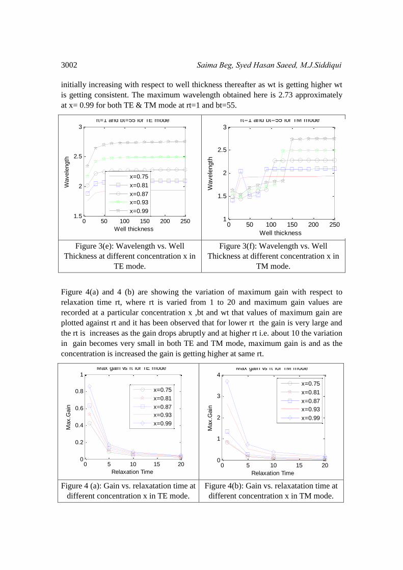
Figure 4(a) and 4 (b) are showing the variation of maximum gain with respect to
relaxation time rt, where rt is varied from 1 to 20 and maximum gain values are
recorded at a particular concentration x ,bt and wt that values of maximum gain are
plotted against rt and it has been observed that for lower rt the gain is very large and
the rt is increases as the gain drops abruptly and at higher rt i.e. about 10 the variation
in gain becomes very small in both TE and TM mode, maximum gain is and as the
concentration is increased the gain is getting higher at same rt.
Figure 4 (a): Gain vs. relaxatation time at
different concentration x in TE mode.
Figure 4(b): Gain vs. relaxatation time at
different concentration x in TM mode.
0 50 100 150 200 2501.5
2
2.5
3
Well thickness
Wavele
ngth
rt=1 and bt=55 for TE mode
x=0.75
x=0.81
x=0.87
x=0.93
x=0.99
0 50 100 150 200 2501
1.5
2
2.5
3
Well thickness
Wavele
ngth
rt=1 and bt=55 for TM mode
x=0.75
x=0.81
x=0.87
x=0.93
x=0.99
0 5 10 15 200
0.2
0.4
0.6
0.8
1
Relaxation Time
Max.G
ain
Max gain vs rt for TE mode
x=0.75
x=0.81
x=0.87
x=0.93
x=0.99
0 5 10 15 200
1
2
3
4
Relaxation Time
Max.G
ain
Max gain vs rt for TM mode
x=0.75
x=0.81
x=0.87
x=0.93
x=0.99
III-V Compound Semiconductor Laser Heterostructures Parametric… 3003
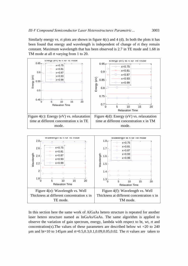
Similarly energy vs. rt plots are shown in figure 4(c) and 4 (d). In both the plots it has
been found that energy and wavelength is independent of change of rt they remain
constant. Maximum wavelength that has been observed is 2.7 in TE mode and 1.68 in
TM mode at all rt varying from 1 to 20.
Figure 4(c): Energy (eV) vs. relaxatation
time at different concentration x in TE
mode.
Figure 4(d): Energy (eV) vs. relaxatation
time at different concentration x in TM
mode.
Figure 4(e): Wavelength vs. Well
Thickness at different concentration x in
TE mode.
Figure 4(f): Wavelength vs. Well
Thickness at different concentration x in
TM mode.
In this section here the same work of AlGaAs hetero structure is repeated for another
laser hetero structure named as InGaAs/GaAs. The same algorithm is applied to
observe the variation of gain spectrum, energy, lambda with respect to bt, wt, rt and
concentration(x).The values of these parameters are described below wt =20 to 240
µm and bt=10 to 145µm and rt=0.5,0.3,0.1,0.09,0.05,0.02. The rt values are taken to
0 5 10 15 200.45
0.5
0.55
0.6
0.65
Relaxation Time
Energ
y (
eV
)
Energy (eV) vs rt for TE mode
x=0.75
x=0.81
x=0.87
x=0.93
x=0.99
0 5 10 15 200.7
0.75
0.8
0.85
0.9
0.95
Relaxation Time
Energ
y (
eV
)
Energy (eV) vs rt for TM mode
x=0.75
x=0.81
x=0.87
x=0.93
x=0.99
0 5 10 15 201.8
2
2.2
2.4
2.6
2.8
Relaxation Time
Wavele
ngth
Wavelength vs rt for TE mode
x=0.75
x=0.81
x=0.87
x=0.93
x=0.99
0 5 10 15 201.3
1.4
1.5
1.6
1.7
1.8
Relaxation Time
Wavele
ngth
Wavelength vs rt for TM mode
x=0.75
x=0.81
x=0.87
x=0.93
x=0.99
3004 Saima Beg, Syed Hasan Saeed, M.J.Siddiqui
be 0.5 and gradually decreased to 0.02 for getting the gain spectrum at different
concentration of x=0.8,0.84,0.87,0.9,0.93,0.96,0.99 for all these parametric values
gain spectrum as a function of lambda are plotted and the maximum gain values is
again recorded at different bt, wt, rt and x.
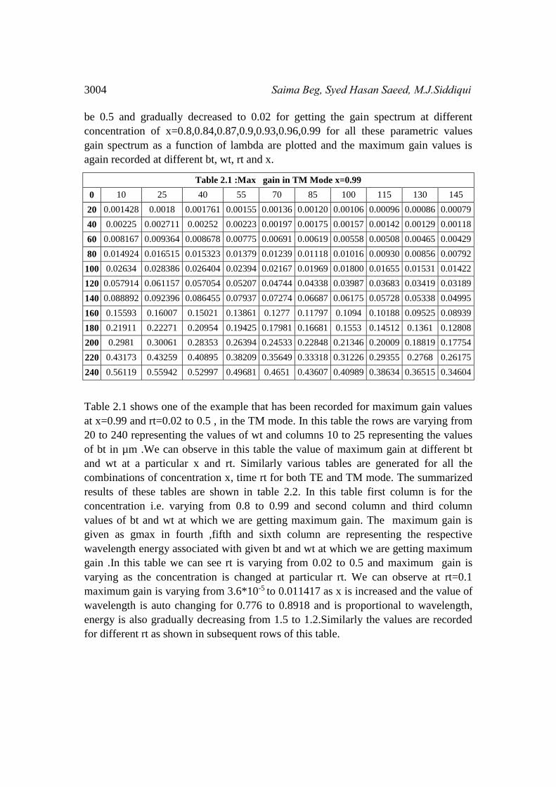
Table 2.1 :Max gain in TM Mode x=0.99
0 10 25 40 55 70 85 100 115 130 145
20 0.001428 0.0018 0.001761 0.00155 0.00136 0.00120 0.00106 0.00096 0.00086 0.00079
40 0.00225 0.002711 0.00252 0.00223 0.00197 0.00175 0.00157 0.00142 0.00129 0.00118
60 0.008167 0.009364 0.008678 0.00775 0.00691 0.00619 0.00558 0.00508 0.00465 0.00429
80 0.014924 0.016515 0.015323 0.01379 0.01239 0.01118 0.01016 0.00930 0.00856 0.00792
100 0.02634 0.028386 0.026404 0.02394 0.02167 0.01969 0.01800 0.01655 0.01531 0.01422
120 0.057914 0.061157 0.057054 0.05207 0.04744 0.04338 0.03987 0.03683 0.03419 0.03189
140 0.088892 0.092396 0.086455 0.07937 0.07274 0.06687 0.06175 0.05728 0.05338 0.04995
160 0.15593 0.16007 0.15021 0.13861 0.1277 0.11797 0.1094 0.10188 0.09525 0.08939
180 0.21911 0.22271 0.20954 0.19425 0.17981 0.16681 0.1553 0.14512 0.1361 0.12808
200 0.2981 0.30061 0.28353 0.26394 0.24533 0.22848 0.21346 0.20009 0.18819 0.17754
220 0.43173 0.43259 0.40895 0.38209 0.35649 0.33318 0.31226 0.29355 0.2768 0.26175
240 0.56119 0.55942 0.52997 0.49681 0.4651 0.43607 0.40989 0.38634 0.36515 0.34604
Table 2.1 shows one of the example that has been recorded for maximum gain values
at x=0.99 and rt=0.02 to 0.5 , in the TM mode. In this table the rows are varying from
20 to 240 representing the values of wt and columns 10 to 25 representing the values
of bt in µm .We can observe in this table the value of maximum gain at different bt
and wt at a particular x and rt. Similarly various tables are generated for all the
combinations of concentration x, time rt for both TE and TM mode. The summarized
results of these tables are shown in table 2.2. In this table first column is for the
concentration i.e. varying from 0.8 to 0.99 and second column and third column
values of bt and wt at which we are getting maximum gain. The maximum gain is
given as gmax in fourth ,fifth and sixth column are representing the respective
wavelength energy associated with given bt and wt at which we are getting maximum
gain .In this table we can see rt is varying from 0.02 to 0.5 and maximum gain is
varying as the concentration is changed at particular rt. We can observe at rt=0.1
maximum gain is varying from 3.6*10-5 to 0.011417 as x is increased and the value of
wavelength is auto changing for 0.776 to 0.8918 and is proportional to wavelength,
energy is also gradually decreasing from 1.5 to 1.2.Similarly the values are recorded
for different rt as shown in subsequent rows of this table.
III-V Compound Semiconductor Laser Heterostructures Parametric… 3005
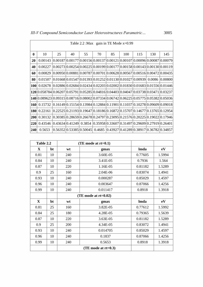
Table 2.2 :Max gain in TE Mode x=0.99
0 10 25 40 55 70 85 100 115 130 145
20 0.00143 0.00187 0.00177 0.00156 0.00137 0.00121 0.00107 0.00096 0.00087 0.00079
40 0.00227 0.00273 0.00254 0.00225 0.00199 0.00177 0.00158 0.00143 0.00130 0.00119
60 0.00829 0.00950 0.00881 0.00787 0.00701 0.00628 0.00567 0.00516 0.00472 0.00435
80 0.01507 0.01668 0.01547 0.01393 0.01252 0.01130 0.01027 0.00939 0.0086 0.00800
100 0.02678 0.02886 0.02684 0.02434 0.02203 0.02002 0.01830 0.01683 0.01556 0.01446
120 0.058784 0.06207 0.05791 0.05285 0.04816 0.04403 0.04047 0.03738 0.03471 0.03237
140 0.089623 0.09315 0.08716 0.08002 0.07334 0.06742 0.06225 0.05775 0.05382 0.05036
160 0.15732 0.16149 0.15154 0.13984 0.12884 0.11901 0.11037 0.10278 0.09609 0.09018
180 0.22161 0.22525 0.21193 0.19647 0.18186 0.16872 0.15707 0.14677 0.13765 0.12954
200 0.30132 0.30385 0.28659 0.26678 0.24797 0.23095 0.21576 0.20225 0.19022 0.17946
220 0.43546 0.43634 0.41249 0.3854 0.35958 0.33607 0.31497 0.29609 0.27919 0.26401
240 0.5653 0.56352 0.53385 0.50045 0.4685 0.43927 0.41289 0.38917 0.36782 0.34857
Table 2.2 (TE mode at rt=0.1)
X bt wt gmax lmda eV
0.81 10 240 3.60E-05 0.77605 1.5994
0.84 10 240 3.41E-05 0.7936 1.564
0.87 10 220 1.16E-05 0.81182 1.5289
0.9 25 160 2.04E-06 0.83074 1.4941
0.93 10 240 0.000287 0.85029 1.4597
0.96 10 240 0.003647 0.87066 1.4256
0.99 10 240 0.011417 0.8918 1.3918
(TE mode at rt=0.02)
X bt wt gmax lmda eV
0.81 25 160 3.82E-05 0.77612 1.5992
0.84 25 180 4.28E-05 0.79365 1.5639
0.87 10 220 3.63E-05 0.81182 1.5289
0.9 25 200 4.34E-05 0.83072 1.4941
0.93 10 240 0.014705 0.85029 1.4597
0.96 10 240 0.1837 0.87066 1.4256
0.99 10 240 0.5653 0.8918 1.3918
(TE mode at rt=0.3)
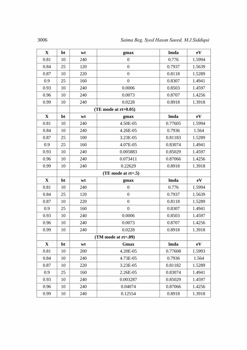
3006 Saima Beg, Syed Hasan Saeed, M.J.Siddiqui
X bt wt gmax Imda eV
0.81 10 240 0 0.776 1.5994
0.84 25 120 0 0.7937 1.5639
0.87 10 220 0 0.8118 1.5289
0.9 25 160 0 0.8307 1.4941
0.93 10 240 0.0006 0.8503 1.4597
0.96 10 240 0.0073 0.8707 1.4256
0.99 10 240 0.0228 0.8918 1.3918
(TE mode at rt=0.05)
X bt wt gmax lmda eV
0.81 10 240 4.50E-05 0.77605 1.5994
0.84 10 240 4.26E-05 0.7936 1.564
0.87 25 100 3.23E-05 0.81183 1.5289
0.9 25 160 4.07E-05 0.83074 1.4941
0.93 10 240 0.005883 0.85029 1.4597
0.96 10 240 0.073411 0.87066 1.4256
0.99 10 240 0.22629 0.8918 1.3918
(TE mode at rt=.5)
X bt wt gmax lmda eV
0.81 10 240 0 0.776 1.5994
0.84 25 120 0 0.7937 1.5639
0.87 10 220 0 0.8118 1.5289
0.9 25 160 0 0.8307 1.4941
0.93 10 240 0.0006 0.8503 1.4597
0.96 10 240 0.0073 0.8707 1.4256
0.99 10 240 0.0228 0.8918 1.3918
(TM mode at rt=.09)
X bt wt Gmax lmda eV
0.81 10 200 4.20E-05 0.77608 1.5993
0.84 10 240 4.73E-05 0.7936 1.564
0.87 10 220 3.23E-05 0.81182 1.5289
0.9 25 160 2.26E-05 0.83074 1.4941
0.93 10 240 0.003287 0.85029 1.4597
0.96 10 240 0.04074 0.87066 1.4256
0.99 10 240 0.12554 0.8918 1.3918
III-V Compound Semiconductor Laser Heterostructures Parametric… 3007
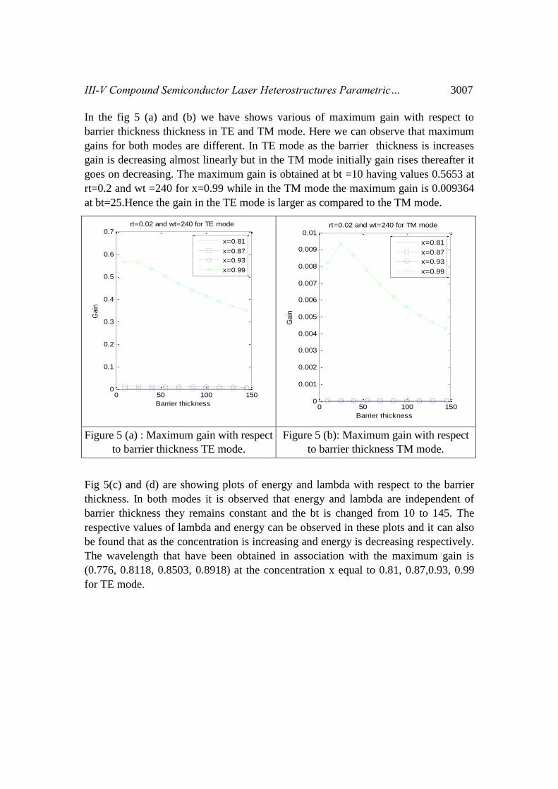
In the fig 5 (a) and (b) we have shows various of maximum gain with respect to
barrier thickness thickness in TE and TM mode. Here we can observe that maximum
gains for both modes are different. In TE mode as the barrier thickness is increases
gain is decreasing almost linearly but in the TM mode initially gain rises thereafter it
goes on decreasing. The maximum gain is obtained at bt =10 having values 0.5653 at
rt=0.2 and wt =240 for x=0.99 while in the TM mode the maximum gain is 0.009364
at bt=25.Hence the gain in the TE mode is larger as compared to the TM mode.
Figure 5 (a) : Maximum gain with respect
to barrier thickness TE mode.
Figure 5 (b): Maximum gain with respect
to barrier thickness TM mode.
Fig 5(c) and (d) are showing plots of energy and lambda with respect to the barrier
thickness. In both modes it is observed that energy and lambda are independent of
barrier thickness they remains constant and the bt is changed from 10 to 145. The
respective values of lambda and energy can be observed in these plots and it can also
be found that as the concentration is increasing and energy is decreasing respectively.
The wavelength that have been obtained in association with the maximum gain is
(0.776, 0.8118, 0.8503, 0.8918) at the concentration x equal to 0.81, 0.87,0.93, 0.99
for TE mode.
0 50 100 1500
0.1
0.2
0.3
0.4
0.5
0.6
0.7
Barrier thickness
Gain
rt=0.02 and wt=240 for TE mode
x=0.81
x=0.87
x=0.93
x=0.99
0 50 100 1500
0.001
0.002
0.003
0.004
0.005
0.006
0.007
0.008
0.009
0.01
Barrier thickness
Gain
rt=0.02 and wt=240 for TM mode
x=0.81
x=0.87
x=0.93
x=0.99
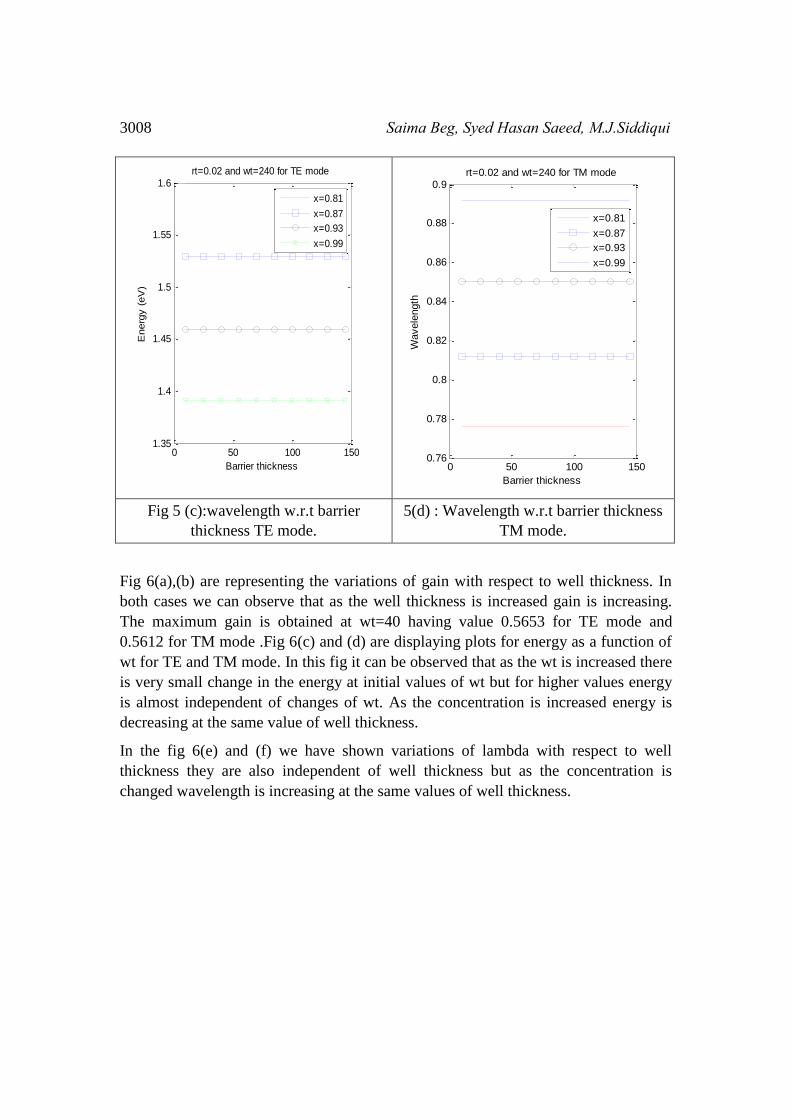
3008 Saima Beg, Syed Hasan Saeed, M.J.Siddiqui
Fig 5 (c):wavelength w.r.t barrier
thickness TE mode.
5(d) : Wavelength w.r.t barrier thickness
TM mode.
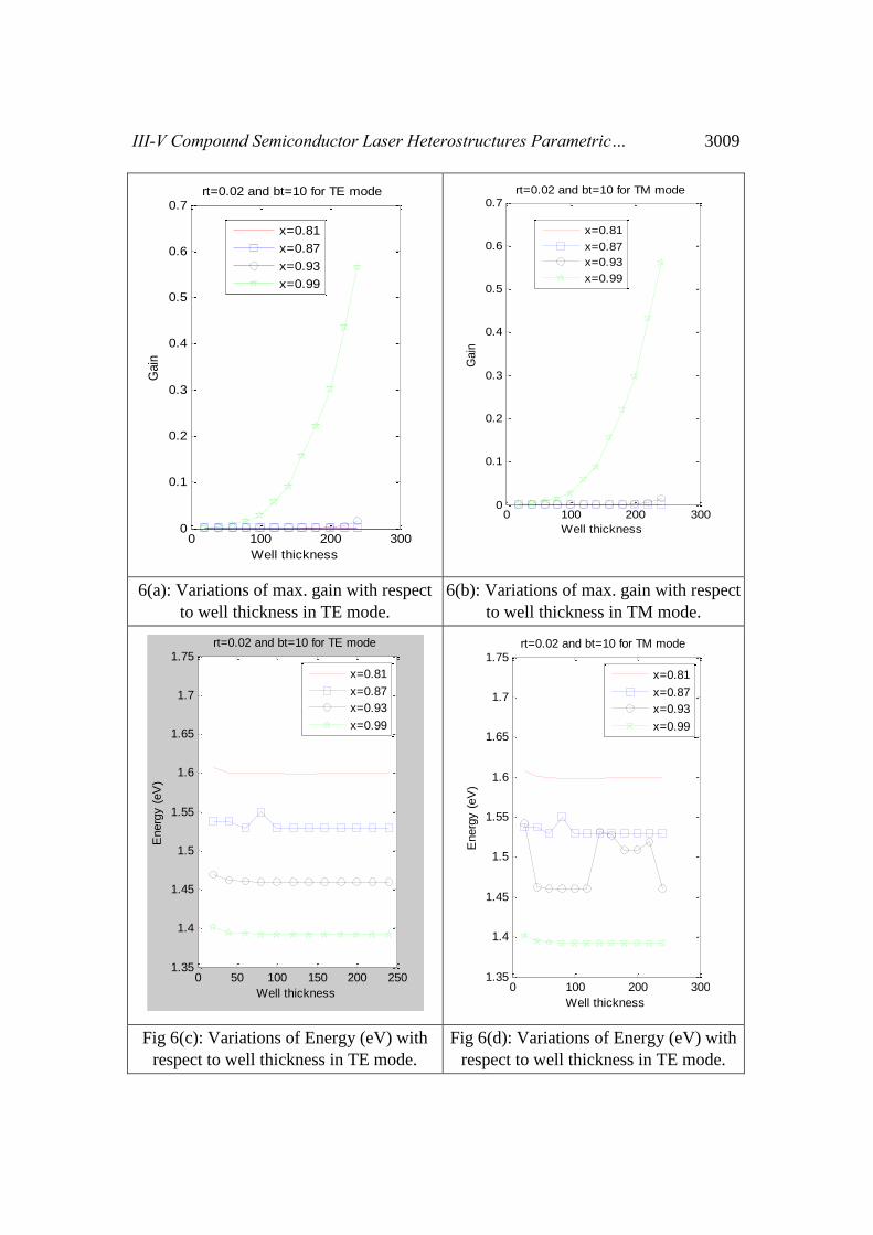
Fig 6(a),(b) are representing the variations of gain with respect to well thickness. In
both cases we can observe that as the well thickness is increased gain is increasing.
The maximum gain is obtained at wt=40 having value 0.5653 for TE mode and
0.5612 for TM mode .Fig 6(c) and (d) are displaying plots for energy as a function of
wt for TE and TM mode. In this fig it can be observed that as the wt is increased there
is very small change in the energy at initial values of wt but for higher values energy
is almost independent of changes of wt. As the concentration is increased energy is
decreasing at the same value of well thickness.
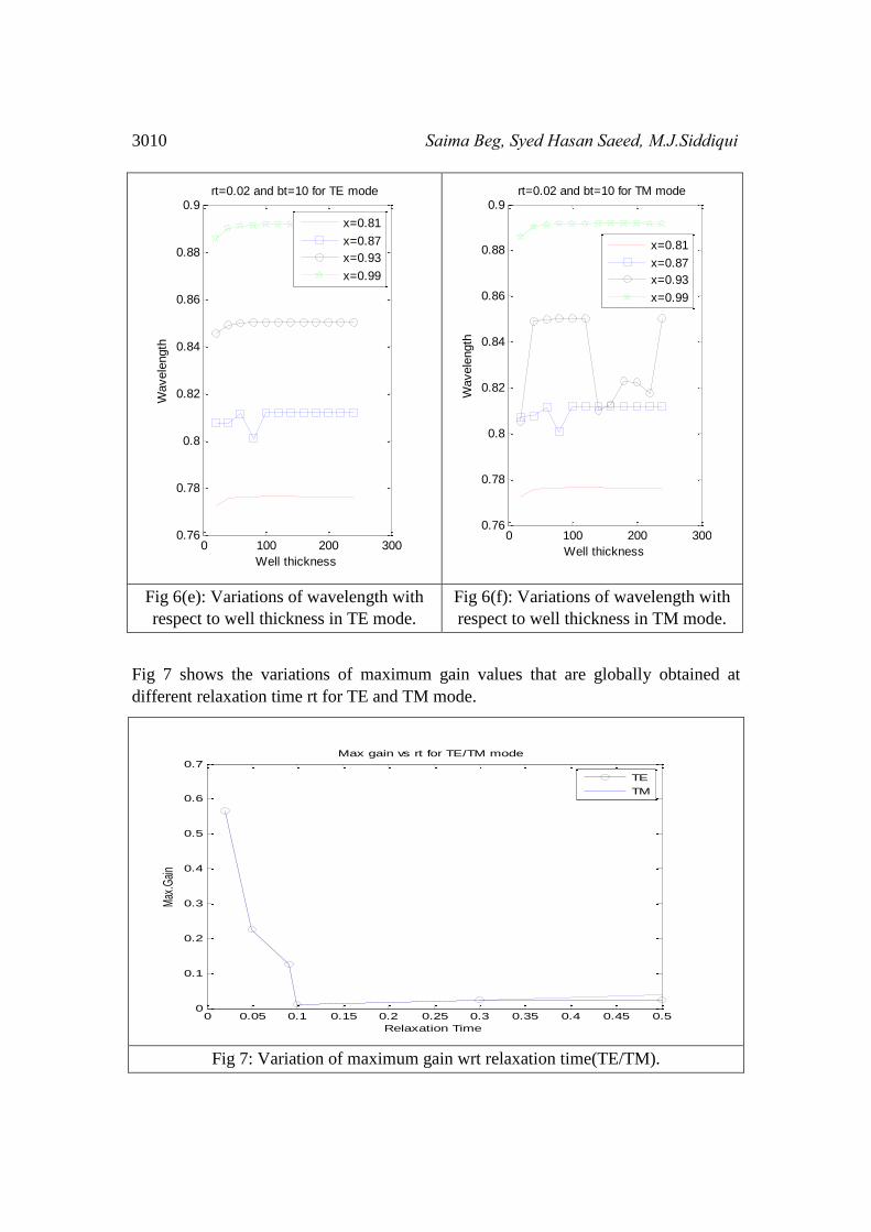
In the fig 6(e) and (f) we have shown variations of lambda with respect to well
thickness they are also independent of well thickness but as the concentration is
changed wavelength is increasing at the same values of well thickness.
0 50 100 1501.35
1.4
1.45
1.5
1.55
1.6
Barrier thickness
Energ
y (
eV
)
rt=0.02 and wt=240 for TE mode
x=0.81
x=0.87
x=0.93
x=0.99
0 50 100 1500.76
0.78
0.8
0.82
0.84
0.86
0.88
0.9
Barrier thickness
Wavele
ngth
rt=0.02 and wt=240 for TM mode
x=0.81
x=0.87
x=0.93
x=0.99
III-V Compound Semiconductor Laser Heterostructures Parametric… 3009
6(a): Variations of max. gain with respect
to well thickness in TE mode.
6(b): Variations of max. gain with respect
to well thickness in TM mode.
Fig 6(c): Variations of Energy (eV) with
respect to well thickness in TE mode.
Fig 6(d): Variations of Energy (eV) with
respect to well thickness in TE mode.
0 100 200 3000
0.1
0.2
0.3
0.4
0.5
0.6
0.7
Well thickness
Gain
rt=0.02 and bt=10 for TE mode
x=0.81
x=0.87
x=0.93
x=0.99
0 100 200 3000
0.1
0.2
0.3
0.4
0.5
0.6
0.7
Well thickness
Gain
rt=0.02 and bt=10 for TM mode
x=0.81
x=0.87
x=0.93
x=0.99
0 50 100 150 200 2501.35
1.4
1.45
1.5
1.55
1.6
1.65
1.7
1.75
Well thickness
Energ
y (
eV
)
rt=0.02 and bt=10 for TE mode
x=0.81
x=0.87
x=0.93
x=0.99
0 100 200 3001.35
1.4
1.45
1.5
1.55
1.6
1.65
1.7
1.75
Well thickness
Energ
y (
eV
)
rt=0.02 and bt=10 for TM mode
x=0.81
x=0.87
x=0.93
x=0.99
3010 Saima Beg, Syed Hasan Saeed, M.J.Siddiqui
Fig 6(e): Variations of wavelength with
respect to well thickness in TE mode.
Fig 6(f): Variations of wavelength with
respect to well thickness in TM mode.
Fig 7 shows the variations of maximum gain values that are globally obtained at
different relaxation time rt for TE and TM mode.
Fig 7: Variation of maximum gain wrt relaxation time(TE/TM).
0 100 200 3000.76
0.78
0.8
0.82
0.84
0.86
0.88
0.9
Well thickness
Wavele
ngth
rt=0.02 and bt=10 for TE mode
x=0.81
x=0.87
x=0.93
x=0.99
0 100 200 3000.76
0.78
0.8
0.82
0.84
0.86
0.88
0.9
Well thickness
Wavele
ngth
rt=0.02 and bt=10 for TM mode
x=0.81
x=0.87
x=0.93
x=0.99
0 0.05 0.1 0.15 0.2 0.25 0.3 0.35 0.4 0.45 0.50
0.1
0.2
0.3
0.4
0.5
0.6
0.7
Relaxation Time
Max
.Gai
n
Max gain vs rt for TE/TM mode
TE
TM
III-V Compound Semiconductor Laser Heterostructures Parametric… 3011
In this fig we can observed that black line is for maximum gain in TE mode and blue
line is for maximum gain in TM mode . Both lines are superimposing each other
hence in both TE and TM mode the respective heterostructures are similar and as the
rt is increased gain is decreasing and maximum gain is obtained at rt=0.02 and as rt is
above than 0.1 maximum gain is nearly constant.
CONCLUSION:
In this work at different parameters we collected maximum gain and wavelength for
two different heterostructure configurations. In GaAs/GaAs / and AlGaAs/GaAs.
Both heterostructures configurations performance with respect to barrier thickness,
well thickness, and relaxation times are separately generated by simulation model to
get more maximum gain condition as output parameters. Wavelengths are collected
with different composition and best well thickness and barrier thickness are found to
analyze the photoluminescence spectra as well as the lasing wavelength of the
devices. AlGaAs/GaAs provides maximum gain at barrier thickness of 40 to 55 nm
.As the well thickness is increased the gain keeps increasing in TE mode but in TM
mode highest gain is achieved at 10nm at lower concentration or at 50nm for higher
concentration x. The gain is higher in TM mode for AlGaAs/GaAs as compared to TE
mode. Wavelength and energy is independent of change in well and barrier thickness
but as the concentration x is increased wavelength decreases and eV is increased. As
the relaxation time is increased gain increases in both TE/TM mode but wavelength
remains constant with respect to relaxation time. Similar observations are also
observed for InGaAs/GaAs.
REFRENCES:
[1] Testsuhiko Ikegami "Reflectivity of Mode at Facet and Oscillation Mode in
Double-Heterostructure Injection Lasers" IEEE Journal of Quantum
Electronics, June 1972.
[2] Rodney S. Tucker, "Circuit model of double-heterojunction laser below
threshold" IEE Proc, Vol. 128, Pt. I, No. 3, June 1981.
[3] Wlodzimierz Nakwaski, " Three-dimensional time-dependent thermal model
of catastrophic mirror damage in stripe-geometry double-heterostructure
GaAs/(AIGa)As diode lasers" Optical and Quantum Electronics 21 (1989)
331-334.
[4] Ching-Fuh Lin, Bor-Lin Lee, and Po-Chien Lin, " Broad-Band
Superluminescent Diodes Fabricated on a Substrate with Asymmetric Dual
Quantum Wells" IEEE Photonics Technology Letters, Vol. 8, No. 11,
3012 Saima Beg, Syed Hasan Saeed, M.J.Siddiqui
November 1996.
[5] Ching-Fuh Lina and Bor-Lin Lee, "Extremely broadband AlGaAs/GaAs
superluminescent diodes" Appl. Phys. Lett. 71 (12), 22 September 1997.
[6] Z. Mi and Y.-L. Chang, "III-V compound semiconductor nanostructures on
silicon: Epitaxial growth, properties, and applications in light emitting diodes
and lasers" Journal of Nanophotonics, Vol. 3, 031602 (23 January 2009).
[7] Christian Grasse, Simeon Katz, Gerhard Bohm, Augustinas Vizbaras, Ralf
Meyer, and Markus-Christian Amann, "Evaluation of injectorless quantum
cascade lasers by combining XRD- and laser-characterisation" Journal
ofCrystalGrowth323(2011)480–483.
[8] Xiaoqing Zhang et. al., " Sum frequency generation in pure zinc-blende GaAs
nanowires" 18 November 2013, Vol. 21, No. 23, DOI:10.1364/OE.21.028432,
Optics Express 28432.
[9] Hung Yew Mun et. al., " Strained Quantum Well Heterostructure: Modeling
and Simulation of 980 nm", ICSE2002 Proc. 2002, Penang, Malaysia.
[10] Agrawal And Bobeck, "Modeling of Distributed Feedback Semiconductor
Lasers with Axially -Varying Parameters", IEEE journal of quantum
electronics. vol 24. No. 12. December 1988.
[11] Wlodzimierz Nakwaski, "Three-dimensional time-dependent thermal model of
catastrophic mirror damage in stripe-geometry double-heterostructure
GaAs/(AIGa)As diode lasers", Optical and Quantum Electronics 21 (1989)
331-334.
[12] Amir Naqwi and Franz Durst, "Focusing of diode laser beams: a simple
mathematical model", Applied Optics / Vol. 29, No. 12 / 20 April 1990.
[13] Ching-Fuh Lin et. al., "Broad-Band Superluminescent Diodes Fabricated On
A Substrate with asymmetric dual quantum wells" IEEE photonics technology
letters, Vol. 8, NO. 11, November 1996.
[14] Ching-Fuh Lin and Bor-Lin Lee, "Extremely broadband AlGaAs/GaAs
superluminescent diodes" Appl. Phys. Lett. 71 (12), 22 September 1997.
[15] V. E. Bougrov and A. S. Zubrilov, "Optical confinement and threshold
currents in III–V nitride heterostructures: Simulation", J. Appl. Phys. 81 (7), 1
April 1997.
[16] P. A. Alvi, "Modal Gain Characteristics of GRIN-InGaAlAs/InP Lasing Nano-
heterostructures", Superlattices and Microstructures 2005.
[17] Allen Hsu et. al., "Four-Well Highly Strained Quantum Cascade Lasers grown
by metal-organic chemical vapor deposition", OSA/CLEO/IQEC 2009
III-V Compound Semiconductor Laser Heterostructures Parametric… 3013
[18] Z. Mi, "III-V compound semiconductor nanostructures on silicon: Epitaxial
growth, properties, and applications in light emitting diodes and lasers",
Journal of Nanophotonics, Vol. 3, 031602 (23 January 2009).
[19] K. Kashani- Shirazi, "Ultra-low-threshold GaSb-based Laser Diodes at 2.65
μm", OSA/CLEO/IQEC 2009.
[20] Neng Liu et. al., "Enhanced photoluminescence emission from band gap
shifted InGaAs/InGaAsP/InP microstructures processed with UV laser
quantum well intermixing", Journal Of Physics D Applied Physics, October
2013.
[21] A. Khaledi-Nasab et. al., "Linear and nonlinear tunable optical properties of
inter subband transitions in GaN/AlN quantum dots in presence and absence
of wetting layer", J. Europ. Opt. Soc. Rap. Public. 9, 14011 (2014).
[22] Bauke W. Tilma, "Recent advances in ultrafast semiconductor disk lasers",
Fine Mechanics and Physics (CIOMP), Chinese Academy of Sciences (CAS)
2015.
[23] R. Passler, phys. stat. sol. (b) 193(1), 135 (1996).
[24] V. K. Kononenko, I. S. Zakharova, ICTP, Trieste, IC/91/63, 26 (1991).
[25] E. O. Kane, Energy band theory, in Handbook on Semiconductors (T. S.
Moss, ed.), New York: North-Holland (1982).
[26] J. Piprek, Semiconductor optoelectronics devices. Introduction to physics and
simulation. Academic Press, Amsterdam (2003).
[27] G. Chris, V. D. Walle, Phys. Rev. B. 39(3), 1871 (1989).
[28] J. M. Luttinger, W. Kohn, J. Phys. Rev. 97(4), 869 (1955).
[29] S. L. Chuang, Phys. Rev. B. 43(12), 9649 (1991).
[30] S. L. Chuang, Physics of photonic devices, Wiley & Sons, Inc., New York
(2009).
[31] C. Y. P. Chao, S. L. Chuang, Phys. Rev. B. 46(7), 4110 (1992).

3014 Saima Beg, Syed Hasan Saeed, M.J.Siddiqui