Embed Size (px)
Citation preview
Metal-insulator-semiconductor heterostructures for plasmonic hot-carrier optoelectronics
F. Pelayo García de Arquer1,2 and Gerasimos Konstantatos1,* 1ICFO-Institut de Ciencies Fotoniques, Castelldefels (Barcelona), Spain
2Currently with the Department of Electrical and Computer Engineering, University of Toronto, Toronto, Ontario M5S 3G4, Canada
Abstract: Plasmonic hot-electron devices are attractive candidates for light-energy harvesting and photodetection applications. For solid state devices, the most compact and straightforward architecture is the metal-semiconductor Schottky junction. However convenient, this structure introduces limitations such as the elevated dark current associated to thermionic emission, or constraints for device design due to the finite choice of materials. In this work we theoretically consider the metal-insulator-semiconductor heterojunction as a candidate for plasmonic hot-carrier photodetection and solar cells. The presence of the insulating layer can significantly reduce the dark current, resulting in increased device performance with predicted solar power conversion efficiencies up to 9%. For photodetection, the sensitivity can be extended well into the infrared by a judicious choice of the insulating layer, with up to 300-fold expected enhancement in detectivity.
©2015 Optical Society of America
OCIS codes: (240.6680) Surface plasmons; (130.0250) Optoelectronics; (350.6050) Solar energy; (040.5160) Photodetectors.
References and links
1. C. Clavero, “Plasmon-induced hot-electron generation at nanoparticle/metal-oxide interfaces for photovoltaic and photocatalytic devices,” Nat. Photonics 8(2), 95–103 (2014).
2. M. L. Brongersma, N. J. Halas, and P. Nordlander, “Plasmon-induced hot carrier science and technology,” Nat. Nanotechnol. 10(1), 25–34 (2015).
3. A. O. Govorov, H. Zhang, and Y. K. Gun’ko, “Theory of photoinjection of hot plasmonic carriers from metal nanostructures into semiconductors and surface molecules,” J. Phys. Chem. C 117(32), 16616–16631 (2013).
4. A. Manjavacas, J. G. Liu, V. Kulkarni, and P. Nordlander, “Plasmon-induced hot carriers in metallic nanoparticles,” ACS Nano 8(8), 7630–7638 (2014).
5. G. V. Hartland, “Optical studies of dynamics in noble metal nanostructures,” Chem. Rev. 111(6), 3858–3887 (2011).
6. Y. Tian and T. Tatsuma, “Plasmon-induced photoelectrochemistry at metal nanoparticles supported on nanoporous TiO2,” Chem. Commun. (Camb.) 2004(16), 1810–1811 (2004).
7. E. Kowalska, R. Abe, and B. Ohtani, “Visible light-induced photocatalytic reaction of gold-modified titanium(IV) oxide particles: action spectrum analysis,” Chem. Commun. (Camb.) 2009(2), 241–243 (2009).
8. T. Toyoda, S. Tsugawa, and Q. Shen, “Photoacoustic spectra of Au quantum dots adsorbed on nanostructured TiO2 electrodes together with the photoelectrochemical current characteristics,” J. Appl. Phys. 105(3), 034314 (2009).
9. C. G. Silva, R. Juárez, T. Marino, R. Molinari, and H. García, “Influence of excitation wavelength (UV or visible light) on the photocatalytic activity of titania containing gold nanoparticles for the generation of hydrogen or oxygen from water,” J. Am. Chem. Soc. 133(3), 595–602 (2011).
10. Y. Ide, M. Matsuoka, and M. Ogawa, “Efficient visible-light-induced photocatalytic activity on gold-nanoparticle-supported layered titanate,” J. Am. Chem. Soc. 132(47), 16762–16764 (2010).
11. J. Lee, S. Mubeen, X. Ji, G. D. Stucky, and M. Moskovits, “Plasmonic photoanodes for solar water splitting with visible light,” Nano Lett. 12(9), 5014–5019 (2012).
12. S. Mubeen, J. Lee, N. Singh, S. Krämer, G. D. Stucky, and M. Moskovits, “An autonomous photosynthetic device in which all charge carriers derive from surface plasmons,” Nat. Nanotechnol. 8(4), 247–251 (2013).
13. Y. Takahashi and T. Tatsuma, “Solid state photovoltaic cells based on localized surface plasmon-induced charge separation,” Appl. Phys. Lett. 99(18), 182110 (2011).
14. P. Reineck, G. P. Lee, D. Brick, M. Karg, P. Mulvaney, and U. Bach, “A solid-state plasmonic solar cell via metal nanoparticle self-assembly,” Adv. Mater. 24(35), 4750–4755 (2012).
#238075 - $15.00 USD Received 14 Apr 2015; revised 20 May 2015; accepted 22 May 2015; published 27 May 2015 (C) 2015 OSA 1 Jun 2015 | Vol. 23, No. 11 | DOI:10.1364/OE.23.014715 | OPTICS EXPRESS 14715
15. F. P. García de Arquer, A. Mihi, D. Kufer, and G. Konstantatos, “Photoelectric energy conversion of plasmon-generated hot carriers in metal-insulator-semiconductor structures,” ACS Nano 7(4), 3581–3588 (2013).
16. S. Mubeen, J. Lee, W.-R. Lee, N. Singh, G. D. Stucky, and M. Moskovits, “On the plasmonic photovoltaic,” ACS Nano 8(6), 6066–6073 (2014).
17. H. Lee, Y. K. Lee, E. Hwang, and J. Y. Park, “Enhanced surface plasmon effect of Ag/TiO 2 nanodiodes on internal photoemission,” J. Phys. Chem. C 118(11), 5650–5656 (2014).
18. F. Pelayo García de Arquer, A. Mihi, and G. Konstantatos, “Molecular interfaces for plasmonic hot electron photovoltaics,” Nanoscale 7(6), 2281–2288 (2015).
19. M. W. Knight, H. Sobhani, P. Nordlander, and N. J. Halas, “Photodetection with active optical antennas,” Science 332(6030), 702–704 (2011).
20. A. Sobhani, M. W. Knight, Y. Wang, B. Zheng, N. S. King, L. V. Brown, Z. Fang, P. Nordlander, and N. J. Halas, “Narrowband photodetection in the near-infrared with a plasmon-induced hot electron device,” Nat. Commun. 4, 1643 (2013).
21. M. W. Knight, Y. Wang, A. S. Urban, A. Sobhani, B. Y. Zheng, P. Nordlander, and N. J. Halas, “Embedding plasmonic nanostructure diodes enhances hot electron emission,” Nano Lett. 13(4), 1687–1692 (2013).
22. H. Chalabi, D. Schoen, and M. L. Brongersma, “Hot-electron photodetection with a plasmonic nanostripe antenna,” Nano Lett. 14(3), 1374–1380 (2014).
23. F. Wang and N. A. Melosh, “Power-independent wavelength determination by hot carrier collection in metal-insulator-metal devices,” Nat. Commun. 4, 1711 (2013).
24. W. Li and J. Valentine, “Metamaterial perfect absorber based hot electron photodetection,” Nano Lett. 14(6), 3510–3514 (2014).
25. Y. K. Lee, C. H. Jung, J. Park, H. Seo, G. A. Somorjai, and J. Y. Park, “Surface plasmon-driven hot electron flow probed with metal-semiconductor nanodiodes,” Nano Lett. 11(10), 4251–4255 (2011).
26. S. Mubeen, G. Hernandez-Sosa, D. Moses, J. Lee, and M. Moskovits, “Plasmonic photosensitization of a wide band gap semiconductor: converting plasmons to charge carriers,” Nano Lett. 11(12), 5548–5552 (2011).
27. A. K. Rath, M. Bernechea, L. Martinez, F. P. G. de Arquer, J. Osmond, and G. Konstantatos, “Solution-processed inorganic bulk nano-heterojunctions and their application to solar cells,” Nat. Photonics 6(8), 529–534 (2012).
28. F. P. G. de Arquer, A. Mihi, and G. Konstantatos, “Multiband tunable large area hot carrier plasmonic-crystal photodetectors,” arXiv:1406.2875 (2014).
29. C. Scales and P. Berini, “Thin-film Schottky barrier photodetector models,” IEEE J. Quantum Electron. 46(5), 633–643 (2010).
30. T. P. White and K. R. Catchpole, “Plasmon-enhanced internal photoemission for photovoltaics: theoretical efficiency limits,” Appl. Phys. Lett. 101(7), 073905 (2012).
31. A. J. Leenheer, P. Narang, N. S. Lewis, and H. A. Atwater, “Solar energy conversion via hot electron internal photoemission in metallic nanostructures: efficiency estimates,” J. Appl. Phys. 115(13), 134301 (2014).
32. C. Berglund and W. Spicer, “Photoemission studies of copper and silver: theory,” Phys. Rev. 136(4A), A1030–A1044 (1964).
33. A. O. Govorov, H. Zhang, H. V. Demir, and Y. K. Gun’ko, “Photogeneration of hot plasmonic electrons with metal nanocrystals: quantum description and potential applications,” Nano Today 9(1), 85–101 (2014).
34. G. Mahan, “Theory of photoemission in simple metals,” Phys. Rev. B 2(11), 4334–4350 (1970). 35. S. M. Sze, Physics of Semiconductor Devices, 2nd ed. (John Wiley & Sons, 1981). 36. J. Shewchun, A. Waxman, and G. Warfield, “Tunneling in MIS structures—I,” Solid-State Electron. 10(12),
1165–1186 (1967). 37. M. A. Green, Solar Cells: Operating Principles, Technology, and System Applications (1982). 38. M. T. Greiner, M. G. Helander, W.-M. Tang, Z.-B. Wang, J. Qiu, and Z.-H. Lu, “Universal energy-level
alignment of molecules on metal oxides,” Nat. Mater. 11(1), 76–81 (2011).
1. Introduction
The exciting phenomena arising from the interaction of light with free electrons in nanostructured metals has driven a very intense research in the field of plasmonics during the last decades. The possibility of harvesting the highly energetic carriers, so-called hot electrons (holes), that result from the non-radiative damping of plasmonic resonances has recently attracted significant attention [1,2]. Upon the excitation of plasmons at a given energy (ħω), a hot-electron population is generated that spans from Ef (Fermi level of the metal) to Ef + ħω (conversely for hot-holes, between Ef + ħω to Ef) [3,4]. If these excited carriers are collected before thermalization occurs by internal photoemission (typically a ps-window interval) [5], they can result in a photocurrent with an spectral response tunable by metal nanostructuring, enabling therefore functionalities beyond those resulting from band-to-band absorption in semiconductors. This is appealing for applications such as light-energy harvesting (photocatalysis [6–12] and photovoltaics [13–18]), and photodetection [19–28]. Initially focused in the area of photocatalysis and photochemistry, research in plasmonic hot-electron devices has recently seen significant advances in the area of solid state photodetection and
#238075 - $15.00 USD Received 14 Apr 2015; revised 20 May 2015; accepted 22 May 2015; published 27 May 2015 (C) 2015 OSA 1 Jun 2015 | Vol. 23, No. 11 | DOI:10.1364/OE.23.014715 | OPTICS EXPRESS 14716
photovoltaic devices, based on a Schottky metal-semiconductor (MS) architecture. Motivated by this, reports that studied the theoretical limits of the performance in these devices emerged that, although yielding different estimates, share one common limitation: the elevated dark current of this architecture [29–31]. In the work presented here we theoretically explore the use of a metal-insulator-semiconductor (MIS) hererostructures for plasmonic hot-electron photodiodes and solar cells. This architecture has already been successfully employed in plasmonic hot-electron solar cells, where the main role of the insulating layer was the passivation of detrimental semiconductor midgap states that hinder the photovoltaic response of otherwise MS diodes [15,18]. Here we show that, on top of this, the insulating layer can be used to increase the performance of plasmonic solar cells by means of dark current reduction, and as leverage for device design for a given choice of metal-semiconductor. Hot-electron photodetection also benefits from this approach, as the sensitivity of the devices can be significantly extended into the infrared.
2. Metal-Semiconductor structure
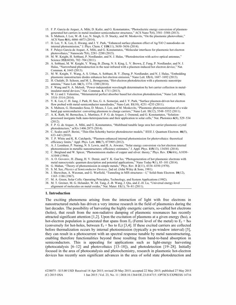
The most straightforward and compact configuration to harvest plasmonic hot-electrons is the metal-semiconductor Schottky junction (Figs. 1(a) and 1(b)). In this structure the hot-electron injection mechanism has been traditionally seen as a three-step process [32]: (i) hot-electrons are generated at a particular place and with a given efficiency within the metal structure. The excitation profile, as well as the energy distribution of hot-electrons, is correlated with the intensity of the electric field [33]. (ii) hot-carriers are emitted with a particular direction, or momentum, depending on the crystal structure [4,21,34] and electric field. (iii) If these energetic electrons arrive at the MS interface with enough momentum, they can be injected or tunnel to the adjacent semiconductor over/through the barrier (Φb), generating a photocurrent.
Fig. 1. Metal-Semiconductor hot-electron plasmonic solar cells. (a) Metal, semiconductor and transparent conductive oxide (TCO) layer before contact. (b) Situation after contact, where a Schottky barrier of height Φb and a buit-in field are established. Plasmonic hot-electrons can be collected when emitted over/through the barrier. (c) Dark current, photocurrent and total current under simulated solar AM 1.5G illumination for a TiO2-Au device.
This process is especially interesting for solar-energy harnessing, since the plasmonic response of photoactive plasmonic structures can be well tuned across the solar spectrum. A number of reports have been published that theoretically explore the efficiency limits of this approach, which basically differ in the hypothesis assumed for each of the aforementioned processes to describe hot-electron photocurrents. The power-conversion-efficiency (PCE) of solar cells is defined as,
( )ph d
inc
J J VPCE
P
+= (1)
#238075 - $15.00 USD Received 14 Apr 2015; revised 20 May 2015; accepted 22 May 2015; published 27 May 2015 (C) 2015 OSA 1 Jun 2015 | Vol. 23, No. 11 | DOI:10.1364/OE.23.014715 | OPTICS EXPRESS 14717
where Jph is the photocurrent, Jd is the dark current, V the applied bias and Pinc the incident power. The photocurrent:
( ) ( )ph inc ph pl pl he t injJ V q V dϕ η η η η λ− −= (2)
where φinc is the power spectral density of the light source (e.g. AM 1.5G solar spectrum), η factors denote the efficiencies of the different wavelength dependent processes (photon to plasmon coupling, plasmon to hot-electron, transport to the interface and injection). The dark current for a metal-semiconductor junction is dominated by the thermionic emission component [35],
* 2( ) exp( / )[exp( / ) 1]th b t tJ V A T qV V Vφ= − − (3)
where A* is the effective Richardson constant (material dependent, empirically determined), T is the operation temperature and Vt = kT/q, k being the Boltzmann constant and q the elementary charge. Theoretically predictions for PCE are scattered depending on the assumptions taken for the different processes involved in Eq. (2). Values bellow 1% (Leenheer et al. [31]) were reported under conservative assumptions regarding hot-electron momentum conservation. This was limited by the rather low emission cone imposed by the range of momentary required to tunnel for perfectly flat interfaces. By relaxing these conditions, which could be reasonable for example in the context of grain boundaries, defects or nanostructured metals, White et al. reported maximum PCE values on the order of 8% in [30]. Given this rather broad interval it is difficult to determine absolute maximum PCE values for plasmonic hot-electron solar cells. For example, by taking into account material considerations such as the electron mean-free-path in the metal the maximum PCE varies from 2.7% (half-space emission) to 5.4% (when all directions are harvested). In the remainder of this manuscript we will stick to the model of White et al. for simplicity, seeking to explore improvements in the maximum PCE under the most optimistic assumptions.
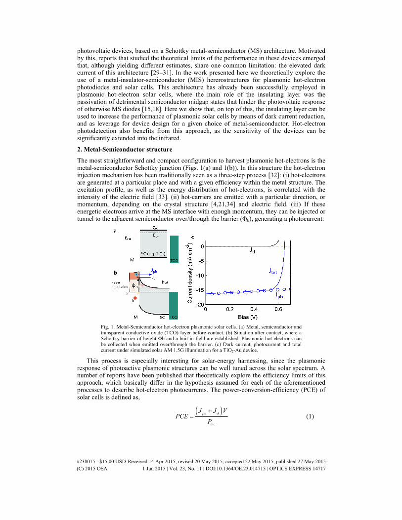
Fig. 2. Photovoltaic figures of merit of MS hot-electron plasmonic solar cells for a TiO2 semiconductor when the barrier is modified. (a) Open-circuit voltage, (b) fill-factor, (c) short-circuit current and (d) power-conversion efficiency (PCE). A maximum PCE of 8% is obtained for a 1.1 eV barrier.
Nevertheless, a common pitfall of these pictures is the elevated dark current associated to thermionic emission. In Fig. 2 we plot the relevant photovoltaic figures of merit for a plasmonic MS solar cell for S = TiO2. This, in combination with the lower fraction of Jph even under the assumption of total absorption of the solar spectrum (note that, in general, for a given energy Eλ, only hot-electrons above Фb will be collected. Hence, only the fraction (Eλ- Фb)/Eλ will effectively contribute to Jph(λ)) demanding over potential values around 0.5 eV
#238075 - $15.00 USD Received 14 Apr 2015; revised 20 May 2015; accepted 22 May 2015; published 27 May 2015 (C) 2015 OSA 1 Jun 2015 | Vol. 23, No. 11 | DOI:10.1364/OE.23.014715 | OPTICS EXPRESS 14718
for a barrier to sustain an open circuit voltage (Fig. 2(a)). On the other hand, for larger barriers the short-circuit current (Jsc = Jd(0) + Jph(0)) is reduced, which results in a maximum PCE of 8% for Фb = 1.1 eV. Reasonable high fill-factors, over 0.6, are obtained for all working configurations.
Although simple and compact, the MS Schottky configuration poses severe constraints for plasmonic hot-electron photovoltaic applications: the elevated dark currents require for large barriers for optimum performance, but only certain barriers can be attained a priori given a particular choice of metal and semiconductor materials (Φb = χsc-Ef). Also very important is, in the case of realistic interfaces, the presence of surface states that result in Fermi level pinning and Фb reduction [15,18]. Therefore, it is important to find alternatives to the MS architecture for more efficient plasmonic hot-electron photovoltaic devices. In the next section we consider the benefits of metal-insulator-semiconductor (MIS) heterostructures for plasmonic solar cells.
3. Metal-Insulator-Semiconductor architecture
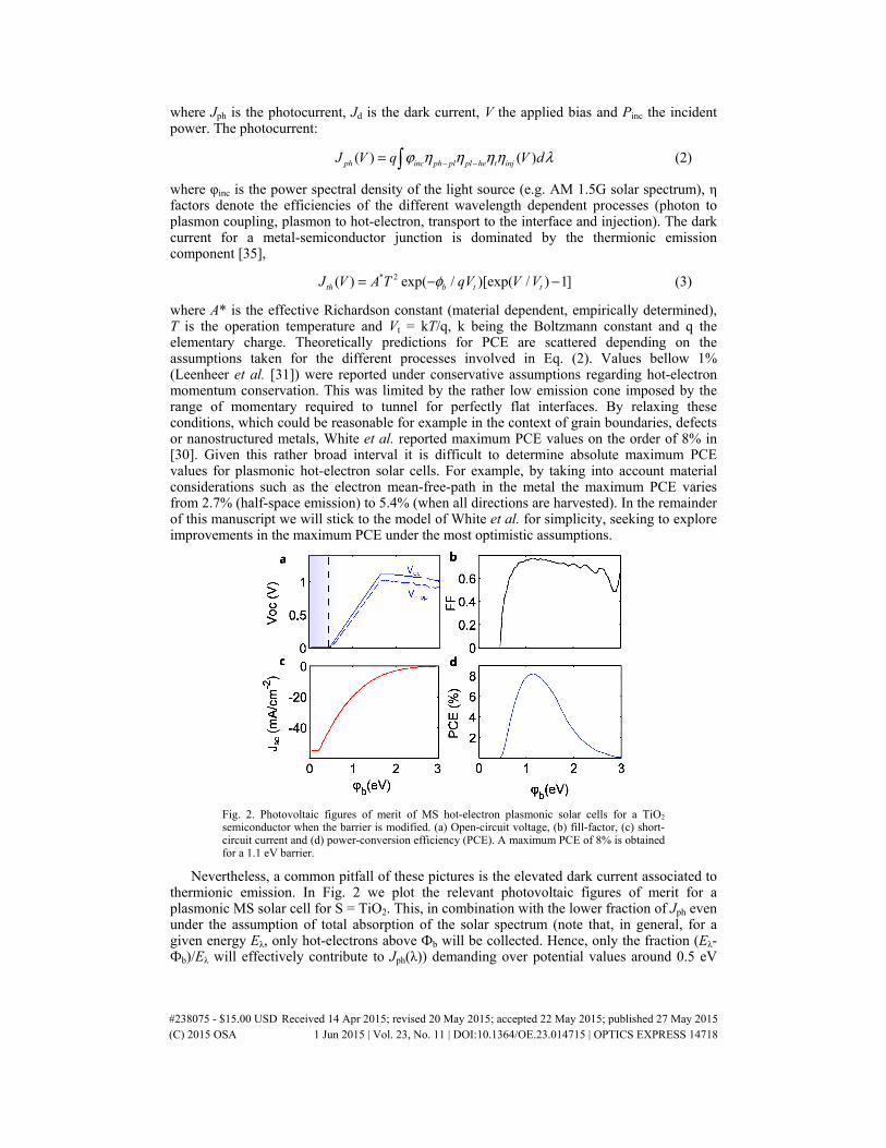
The use of MIS structures was first introduced for photovoltaic applications in the context of silicon MS solar cells to overcome detrimental states due to grain boundaries at the interface [36]. Since then, it was extensively studied as a way to increase the open-circuit voltage and reduce back recombination in other type of solar cells, and recently for plasmonic hot-electron photovoltaics [15,18]. It consists of an insulating layer sandwiched between the metal and the semiconductor, of a given electron affinity (χ) and thickness (d). The dark current in this architecture resembles that of a p-n junction and is dominated by the diffusion term depending on χ and d [37].
d th diffJ J J= + (4)
* 2 exp( / )[exp( / ) 1]th h b t scJ P A T V V Vφ′= − − (5)
2
[exp( / ) 1]h idiff sc t
d h
D nJ q V V
N L= − (6)
Fig. 3. Photovoltaic figures of merit of MS hot-electron plasmonic solar cells for a TiO2 semiconductor when the barrier is modified. (a) Open-circuit voltage, (b) fill-factor, (c) short-circuit current and (d) power-conversion efficiency (PCE). A maximum PCE of 8% is obtained for a 1.1 eV barrier.
where Ph is the tunneling probability for thermally excited electrons (typically calculated as exp(-θ1/2d), θ tunneling barrier height in eV and d in Angstrons) and Vsc is the voltage drop in
#238075 - $15.00 USD Received 14 Apr 2015; revised 20 May 2015; accepted 22 May 2015; published 27 May 2015 (C) 2015 OSA 1 Jun 2015 | Vol. 23, No. 11 | DOI:10.1364/OE.23.014715 | OPTICS EXPRESS 14719
the semiconductor (which depends on the resistance of both insulating and semiconducting layers). Dh is the diffusion coefficient, ni and Nd are the intrinsic and majority carrier concentrations respectively. Lh is the diffusion length. Figure 3(c) showcases how the dark current is modified for different insulator configurations. As the insulating layer barrier is physically thicker or energetically higher the dark current is significantly reduced in an exponential fashion. On the other hand, the presence of the insulating layer is also expected to affect the photocurrent. Only the fraction of hot-electrons with energies above the barrier will be emitted to the semiconductor, and electrons with energies bellow this threshold will undergo quantum tunneling through the insulator. The tunneling probability can be obtained under the WKB approximation as,
2
( , )
2 0
8( , ) exp( 2 ) ( ) )
d E V
inj
mE V E E x dx
h
πη = − − (7)
where m is the electron effective mass and E(x) describes the potential of the barrier as a function of longitudinal distance x. The barrier profile depends on χ and d.
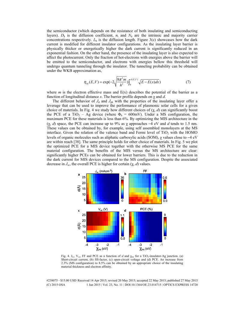
The different behavior of Jd and Jph with the properties of the insulating layer offer a leverage that can be used to improve the performance of plasmonic solar cells for a given choice of materials. In Fig. 4 we study how different choices of (χ, d) can significantly boost the PCE of a TiO2 – Ag device (where Φb = 600mV). Under a MS configuration, the maximum PCE for these materials is less than 6%. By optimizing the MIS architecture in the (χ, d) space, the PCE can increase up to 9% as χ approaches −4 eV and d tends to 1.5 nm. These values can be obtained by, for example, using self assembled monolayers at the MS interface. Given the relation of the valence band and Fermi level of TiO2 with the HOMO levels of organic molecules such as aliphatic carboxylic acids (SOM), χ values close to −4 eV are within reach [38]. The same principle holds for other choice of materials. In Fig. 5 we plot the optimized PCE for a MIS device together with the otherwise MS PCE for the same material configuration. The benefits of the MIS versus the MS architecture are clear: significantly higher PCEs can be obtained for lower barriers. This is due to the reduction in the dark current for MIS devices compared to the MS configuration. Despite the associated decrease in Jsc, the overall PCE is higher for certain (χ, d) values.
Fig. 4. Jsc, Voc, FF and PCE as a function of d and χins for a TiO2-insulator-Ag junction. (a) Short-circuit current, (b) fill-factor, (c) open-circuit voltage and (d) PCE. An increase from 2.3% (MS configuration) to 8.5% can be obtained by an appropriate choice of the insulating material thickness and electron affinity.
#238075 - $15.00 USD Received 14 Apr 2015; revised 20 May 2015; accepted 22 May 2015; published 27 May 2015 (C) 2015 OSA 1 Jun 2015 | Vol. 23, No. 11 | DOI:10.1364/OE.23.014715 | OPTICS EXPRESS 14720
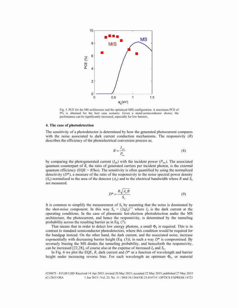
Fig. 5. PCE for the MS architecture and the optimized MIS configuration. A maximum PCE of 9% is obtained for the best case scenario. Given a metal-semiconductor choice, the performance can be significantly increased, especially for low barriers.
4. The case of photodetection
The sensitivity of a photodetector is determined by how the generated photocurrent compares with the noise associated to dark current conduction mechanisms. The responsivity (R) describes the efficiency of the photoelectrical conversion process as,
ph
inc
IR
P= (8)
by comparing the photogenerated current (Iph) with the incident power (Pinc). The associated quantum counterpart of R, the ratio of generated carriers per incident photon, is the external quantum efficiency (EQE = R/ħω). The sensitivity is often quantified by using the normalized detectivity (D*), a measure of the ratio of the responsivity to the noise spectral power density (Sn) normalized to the area of the detector (Ad) and to the electrical bandwidth where R and Sn are measured.
* d
n
R A BD
S= (9)
It is common to simplify the measurement of Sn by assuming that the noise is dominated by the shot-noise component. In this way Sn = (2qId)
1/2 where Id is the dark current at the operating conditions. In the case of plasmonic hot-electron photodetection under the MS architecture, the photocurrent, and hence the responsivity, is determined by the tunneling probability across the resulting barrier as in Eq. (7).
That means that in order to detect low energy photons, a small Φb is required. This is in contrast to standard semiconductor photodetectors, where this condition would be required for the bandgap instead. On the other hand, the dark current, and the associated noise, increase exponentially with decreasing barrier height (Eq. (3)), in such a way D* is compromised. By reversely biasing the MS diodes the tunneling probability, and henceforth the responsivity, can be increased [22,28], of course also at the expense of increased Id and Sn.
In Fig. 6 we plot the EQE, R, dark current and D* as a function of wavelength and barrier height under increasing reverse bias. For each wavelength an optimum Φb, or material
#238075 - $15.00 USD Received 14 Apr 2015; revised 20 May 2015; accepted 22 May 2015; published 27 May 2015 (C) 2015 OSA 1 Jun 2015 | Vol. 23, No. 11 | DOI:10.1364/OE.23.014715 | OPTICS EXPRESS 14721
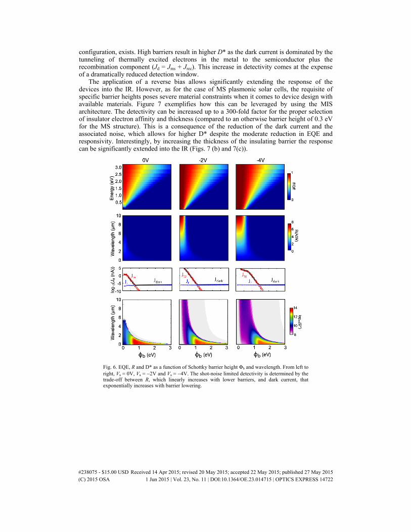
configuration, exists. High barriers result in higher D* as the dark current is dominated by the tunneling of thermally excited electrons in the metal to the semiconductor plus the recombination component (Jd = Jms + Jrec). This increase in detectivity comes at the expense of a dramatically reduced detection window.
The application of a reverse bias allows significantly extending the response of the devices into the IR. However, as for the case of MS plasmonic solar cells, the requisite of specific barrier heights poses severe material constraints when it comes to device design with available materials. Figure 7 exemplifies how this can be leveraged by using the MIS architecture. The detectivity can be increased up to a 300-fold factor for the proper selection of insulator electron affinity and thickness (compared to an otherwise barrier height of 0.3 eV for the MS structure). This is a consequence of the reduction of the dark current and the associated noise, which allows for higher D* despite the moderate reduction in EQE and responsivity. Interestingly, by increasing the thickness of the insulating barrier the response can be significantly extended into the IR (Figs. 7 (b) and 7(c)).
Fig. 6. EQE, R and D* as a function of Schottky barrier height Φb and wavelength. From left to right, Va = 0V, Va = −2V and Va = −4V. The shot-noise limited detectivity is determined by the trade-off between R, which linearly increases with lower barriers, and dark current, that exponentially increases with barrier lowering.
#238075 - $15.00 USD Received 14 Apr 2015; revised 20 May 2015; accepted 22 May 2015; published 27 May 2015 (C) 2015 OSA 1 Jun 2015 | Vol. 23, No. 11 | DOI:10.1364/OE.23.014715 | OPTICS EXPRESS 14722
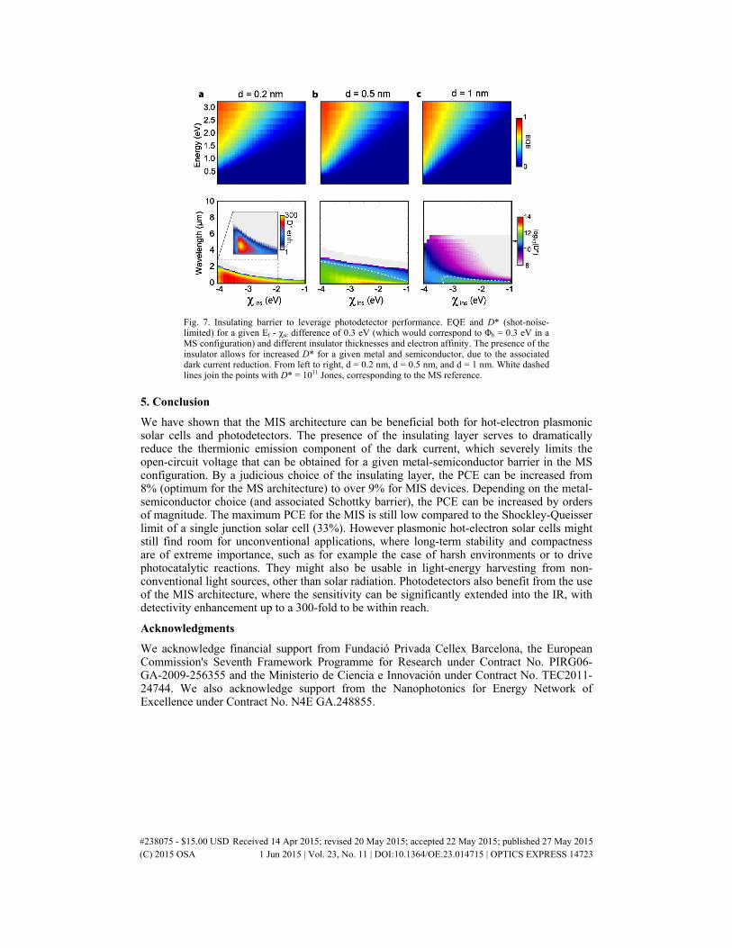
Fig. 7. Insulating barrier to leverage photodetector performance. EQE and D* (shot-noise-limited) for a given Ef - χsc difference of 0.3 eV (which would correspond to Φb = 0.3 eV in a MS configuration) and different insulator thicknesses and electron affinity. The presence of the insulator allows for increased D* for a given metal and semiconductor, due to the associated dark current reduction. From left to right, d = 0.2 nm, d = 0.5 nm, and d = 1 nm. White dashed lines join the points with D* = 1011 Jones, corresponding to the MS reference.
5. Conclusion
We have shown that the MIS architecture can be beneficial both for hot-electron plasmonic solar cells and photodetectors. The presence of the insulating layer serves to dramatically reduce the thermionic emission component of the dark current, which severely limits the open-circuit voltage that can be obtained for a given metal-semiconductor barrier in the MS configuration. By a judicious choice of the insulating layer, the PCE can be increased from 8% (optimum for the MS architecture) to over 9% for MIS devices. Depending on the metal-semiconductor choice (and associated Schottky barrier), the PCE can be increased by orders of magnitude. The maximum PCE for the MIS is still low compared to the Shockley-Queisser limit of a single junction solar cell (33%). However plasmonic hot-electron solar cells might still find room for unconventional applications, where long-term stability and compactness are of extreme importance, such as for example the case of harsh environments or to drive photocatalytic reactions. They might also be usable in light-energy harvesting from non-conventional light sources, other than solar radiation. Photodetectors also benefit from the use of the MIS architecture, where the sensitivity can be significantly extended into the IR, with detectivity enhancement up to a 300-fold to be within reach.
Acknowledgments
We acknowledge financial support from Fundació Privada Cellex Barcelona, the European Commission's Seventh Framework Programme for Research under Contract No. PIRG06-GA-2009-256355 and the Ministerio de Ciencia e Innovación under Contract No. TEC2011-24744. We also acknowledge support from the Nanophotonics for Energy Network of Excellence under Contract No. N4E GA.248855.
#238075 - $15.00 USD Received 14 Apr 2015; revised 20 May 2015; accepted 22 May 2015; published 27 May 2015 (C) 2015 OSA 1 Jun 2015 | Vol. 23, No. 11 | DOI:10.1364/OE.23.014715 | OPTICS EXPRESS 14723