Embed Size (px)
Citation preview
i
IGNITRON TRIGGER CIRCUIT
by
John F. O’Hara III
Senior Project
ELECTRICAL ENGINEERING DEPARTMENT
California Polytechnic State University
San Luis Obispo
June, 2012

i
Table of Contents Table of Contents ........................................................................................................................................... i
List of Tables and Figures ............................................................................................................................. ii
Abstract ........................................................................................................................................................ iii
Acknowledgements ...................................................................................................................................... iv
CHAPTER 1 - INTRODUCTION ............................................................................................................. 1
1.1 Electromagnetic Rail Gun Triggering Circuit ............................................................................ 1
1.2 Background ................................................................................................................................ 2
CHAPTER 2 – SYSTEM COMPONENT DESIGN ................................................................................ 3
2.1 Ignitron ....................................................................................................................................... 3
2.2 Arduino ...................................................................................................................................... 3
2.3 TTL Inverter .............................................................................................................................. 4
2.4 Monostable Multivibrator .......................................................................................................... 5
2.5 MOSFET Driver ........................................................................................................................ 8
2.6 Insulated Gate Bipolar Transistor .............................................................................................. 9
2.8 Transformer ............................................................................................................................. 12
2.9 Voltage Regulator .................................................................................................................... 15
CHAPTER 3 – IMPLEMENTATION AND TESTING ....................................................................... 19
3.1 Implementation ........................................................................................................................ 19
3.2 Testing ..................................................................................................................................... 22
CHAPTER 4 – CONCLUSION ............................................................................................................... 34
BIBLIOGRAPHY ..................................................................................................................................... 35
APPENDIX A COST LIST ...................................................................................................................... 36
APPENDIX B ARDUINO CODE ............................................................................................................ 37

ii
List of Figures
Figure 1: TTL Inverter Circuit ......................................................................................................................... 5
Figure 2: Monostable Multivibrator Circuit .................................................................................................. 6
Figure 3: Current System with TTL Inverter and Monostable Multivibrator ................................................ 7
Figure 4: MOSFET Driver Circuit .................................................................................................................... 9
Figure 5: Current System with TTL Inverter, Monostable Multivibrator, and MOSFET Driver ..................... 9
Figure 6: IGBT Circuit .................................................................................................................................. 10
Figure 7: Current System with TTL Inverter, Monostable Multivibrator, MOSFET Driver, and IGBT ......... 13
Figure 8: Transformer Circuit ...................................................................................................................... 15
Figure 9: Picture of Completed Transformer .............................................................................................. 15
Figure 10: Completed Ignitron Trigger Circuit ............................................................................................ 18
Figure 11: 5V Voltage Regulator ................................................................................................................. 20
Figure 12: 15V Voltage Regulator ............................................................................................................... 21
Figure 13: 8V Voltage Regulator ................................................................................................................. 22
Figure 14: Ignitron Trigger Circuit on Breadboard ...................................................................................... 23
Figure 15: Ignitron Trigger Circuit on Final Board ....................................................................................... 24
Figure 16: Ignitron Mounting Hardware ..................................................................................................... 25
Figure 17: Ignitron Mounting Side View ..................................................................................................... 26
Figure 18: Arduino Output .......................................................................................................................... 27
Figure 19: TTL Inverter Output.................................................................................................................... 28
Figure 20: Monostable Multivibrator Output ............................................................................................. 29
Figure 21: MOSFET Driver Output .............................................................................................................. 30
Figure 22: IGBT Output ............................................................................................................................... 31
Figure 23: 5V Voltage Regulator Output ..................................................................................................... 32
Figure 24: 15V Voltage Regulator Output ................................................................................................... 33
Figure 25: 8V Voltage Regulator Output ..................................................................................................... 34
Figure 26: Transformer Testing ................................................................................................................... 35
Figure 27: Ignitron 10V Charge ................................................................................................................... 36
Figure 28: Ignitron 50V Charge ................................................................................................................... 37
Figure 29: Ignitron 100V Charge ................................................................................................................. 37

iii
Abstract
For my senior project, I will be constructing an Ignitron Triggering Circuit (ITC) for the
rail gun that was developed on campus by an AERO Master student. I will be designing a system
that can be used with either a capacitor or mechanical discharge system. In order to future- proof
the system, it will be designed for the ITC to be compatible with the rail gun Mark 2, which will
use a 12 kV capacitor bank.
The purpose of this project is to provide an alternative to the nitrogen injection system
used on the current rail gun. The proposed ITC will be more efficient and will eliminate the
plasma plume, which in turn will help with data collection.

iv
Acknowledgements
I would like to thank Nolan Uchizono for all of his help in the design and implementation
of the ITC. I would also like to express my appreciation to Dr. Ali Shaban for his assistance as
my Senior Project advisor, and Jeff Maniglia for his work on the rail gun. Finally, I would like to
thank my parents for their support throughout my time here at Cal Poly.

1
CHAPTER 1 – INTRODUCTION
1.1 Electromagnetic Rail Gun Triggering Circuit
An electromagnetic rail gun (EMRG) operates by applying a very high voltage across a
pair of conductive rails in the barrel of the gun. A projectile made out of conductive material is
placed between the rails, which completes the circuit. This completed circuit induces a large
magnetic field from the current traveling through the rails and the projectile, which will help to
accelerate the projectile. Since the projectile is in the rails for a very short period of time, a
pulsed power system is used to power the EMRG.
A pulsed power system is one that accumulates energy in the kJ range and then releases it
in a very short period of time. Pulsed power is used in many different fields beyond rail guns.
Some of the larger fields are radar, pulsed lasers, particle accelerators, and fusion research. Two
of the most common forms of energy storage for pulsed power systems are capacitive and
mechanical, both of which the Cal Poly Pulsed Power team is working on. The triggering circuit
will allow us to choose which energy storage method we would like to test fire, with minimum
work for set up. The switching circuit will also allow us to remove the current, less efficient,
injection system.

2
1.2 Background
Currently, the pulsed power circuit is completed through the injection of the projectile
into the rails with a 3,000 psi nitrogen injection system. Under this current firing system, the
projectile rattles down the barrel, which causes losses due to approximately half of the projectile
melting and being left on the rails as it travels downward. We also have an arcing problem since
the projectile is no longer in constant contact with each side of the rail gun.
The Ignitron triggering circuit will provide an alternative to the current nitrogen injection
system, and permit a projectile to be press-fit into the rails, which will provide greater
conductivity. This will also help to reduce the rattle of the projectile. Under the current system,
there is a large plasma plume that exits the end of the barrel, which prohibits us from using break
screens to get velocity measurements. The plasma sticks to the sheets, and continues to conduct
after the projectile has passed through, which renders the timing data useless. We will also be
reducing the cost of each firing due to the fact that we will no longer need to have nitrogen
refilled each time we would like to fire the rail gun. See Appendix A for the cost breakdown of
this project. This will allow for more testing to be done with the rail gun.

3
CHAPTER 2 – SYSTEM COMPONENT DESIGN
2.1 Ignitron
The Ignitrons are the main system component that the rest of the triggering circuit will be
designed around. Four National Electronics NL7218H-100 Ignitrons have been loaned to the
project from an Orange County power company. These ignitrons allow for switching up to 15
kilovolts and have peak currents of up to 100 kilo amperes, which is more than enough for the
capacitive and mechanical discharge systems. In order to have the ignitrons trigger, and allow the
discharge from the mechanical or capacitive discharge, we must supply at least a 5 µS pulse with
a minimum voltage rating of 1500V. These constraints are what the entire ignitron triggering
circuit has been designed to meet.
2.2 Arduino
An Arduino was chosen to act as the trigger for the circuit, and send the initial pulse. This
eliminates the problem of ringing that occurred when a push button was used. By using an
Arduino we can have multiple safety checks built into the triggering circuit, which will prevent
the accidental triggering of the circuit and the firing of the rail gun. Once the compulsator is
completed, we will have the entire firing mechanism automated so that by a one- button press,
the compulsator will spin up, data collection will begin, and the ignitrons will fire. This saves
time, and allows us to record more useful data without getting multiple seconds of noise in the
data acquisition controller. The Arduino code is listed in Appendix B. As seen from the code, it
waits in a static state until the start button is pressed, and once that has happened, it switches
over to the state that fires the ignitrons. Once this is complete, the compulsator goes into a

4
waiting state for 30 seconds, to make sure there is no longer any ringing from the button press,
before returning to the state of waiting for the push button to trigger it.
2.3 TTL Inverter
In order for the one-shot chip to fire correctly, it needs an inverted TTL input. In the
design of the TTL Inverter we used two MPSA06 npn general purpose amplifiers, along with
4.7kΩ and 1kΩ resistors. Figure 1 shows the circuit diagram for the TTL Inverter. A +5V rail
was used on the top, with ground on the bottom. The wire on the left shows the input from the
Arduino, while the wire on the right connects to the Monostable multivibrator. In order to design
the inverter without the external power supply needed for a 5V rail, we decided to have one
voltage coming in, and to use three different voltage regulators to dial in the specific voltages we
needed.
5
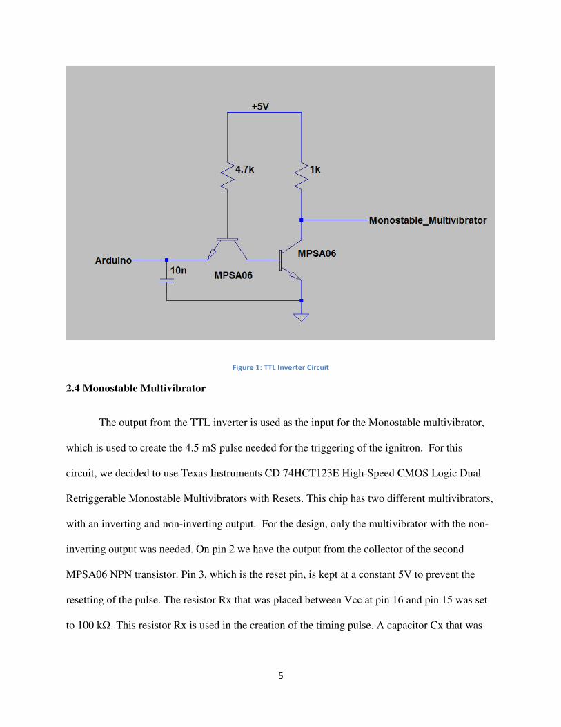
Figure 1: TTL Inverter Circuit
2.4 Monostable Multivibrator
The output from the TTL inverter is used as the input for the Monostable multivibrator,
which is used to create the 4.5 mS pulse needed for the triggering of the ignitron. For this
circuit, we decided to use Texas Instruments CD 74HCT123E High-Speed CMOS Logic Dual
Retriggerable Monostable Multivibrators with Resets. This chip has two different multivibrators,
with an inverting and non-inverting output. For the design, only the multivibrator with the non-
inverting output was needed. On pin 2 we have the output from the collector of the second
MPSA06 NPN transistor. Pin 3, which is the reset pin, is kept at a constant 5V to prevent the
resetting of the pulse. The resistor Rx that was placed between Vcc at pin 16 and pin 15 was set
to 100 kΩ. This resistor Rx is used in the creation of the timing pulse. A capacitor Cx that was

6
set to 100 nF was connected across pins 15 and 14. This capacitor allowed us to have the timing
pulse of 4.5 mS. The formula that gives the pulse length is:
0.45
0.45100 10100 10
4.5 10
4.5
The output from the one-shot circuit is on pin 13. We use this output to feed the MOSFET driver,
which will be discussed later. Figure 2 below illustrates the one-shot section of the ignitron
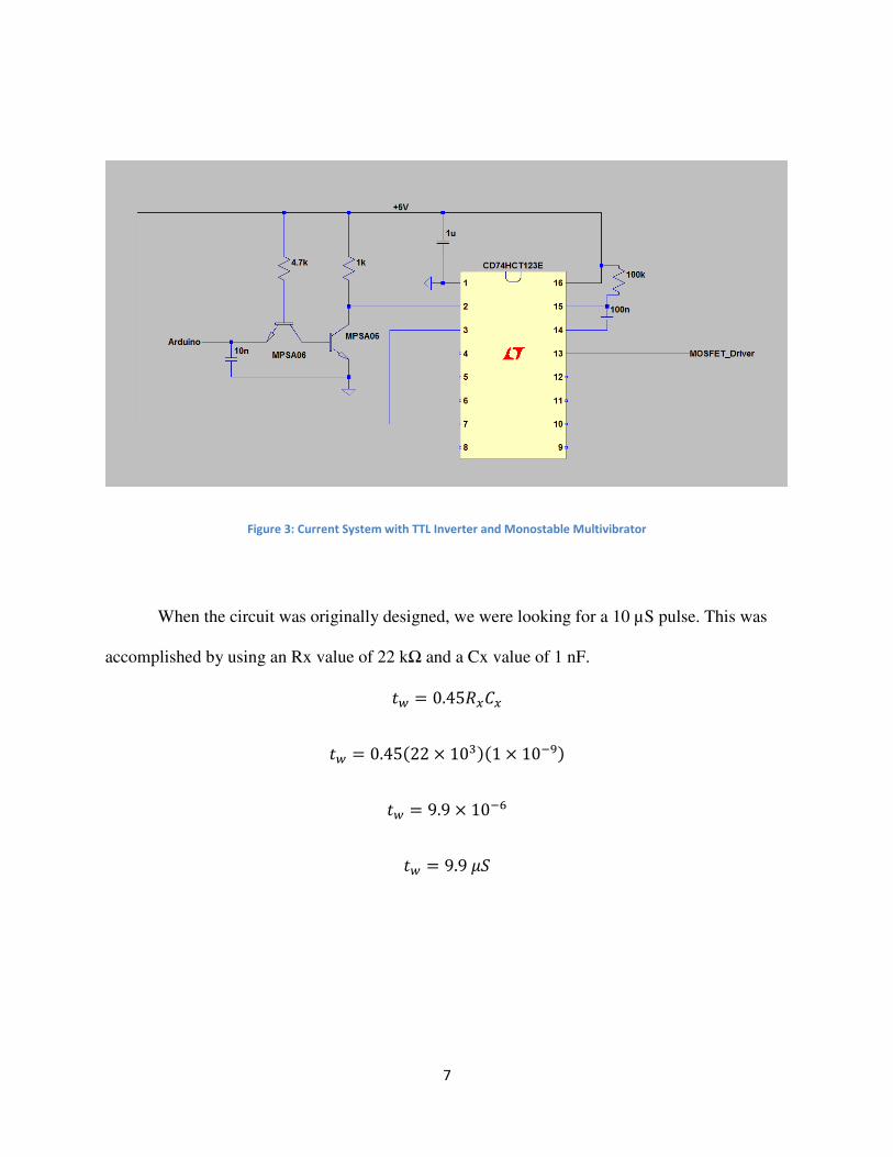
triggering circuit. Figure 3 shows the completed circuit up to this point, including both the TTL
inverter and the Monostable multivibrator.
Figure 2: Monostable Multivibrator Circuit
7
Figure 3: Current System with TTL Inverter and Monostable Multivibrator
When the circuit was originally designed, we were looking for a 10 µS pulse. This was
accomplished by using an Rx value of 22 kΩ and a Cx value of 1 nF.
0.45
0.4522 101 10
9.9 10
9.9

8
This configuration with the 10 µS pulse caused a negative spike to occur when the pulse was
completed. In order to avoid this problem, the pulse length was changed to 4.5 mS. which
allowed normal operation of the circuit.
2.5 MOSFET Driver
The MOSFET Driver that was chosen for the circuit was the Micrel MIC5021 High-
Speed High-Side MOSFET Driver. This chip was selected due to the need for a high-speed
driver for the Insulated-Gate Bipolar Transistors or IGBTs. We will be using this to drive 3
IGBTs in parallel, which are used as one of the final steps in the ignitron triggering circuit. For
the configuration of this chip, pin 2, which is the input was connected to pin 13 from the
Monostable multivibrator. Pins 4 and 5 were connected to ground, while pins 1 and 8 were
connected to the 15V rail coming from the second voltage regulator. Pin 3 was left unconnected.
In order to reduce some of the noise, a 4.7 µF capacitor was placed from the 15V rail to ground.
Pins 6 and 7 were the output, which were connected to the IGBTs. Figure 4 shows the MOSFET
Driver and the connections to it, while Figure 5 illustrates the completed circuit up to this point.
9
Figure 4: MOSFET Driver Circuit
Figure 5: Current System with TTL Inverter, Monostable Multivibrator, and MOSFET Driver
2.6 Insulated Gate Bipolar Transistor
For the final step of the circuit before the transformer, three IGBTs in parallel were used.
International Rectifier IRGPS60B120KD IGBTs were chosen, as they have been found to work
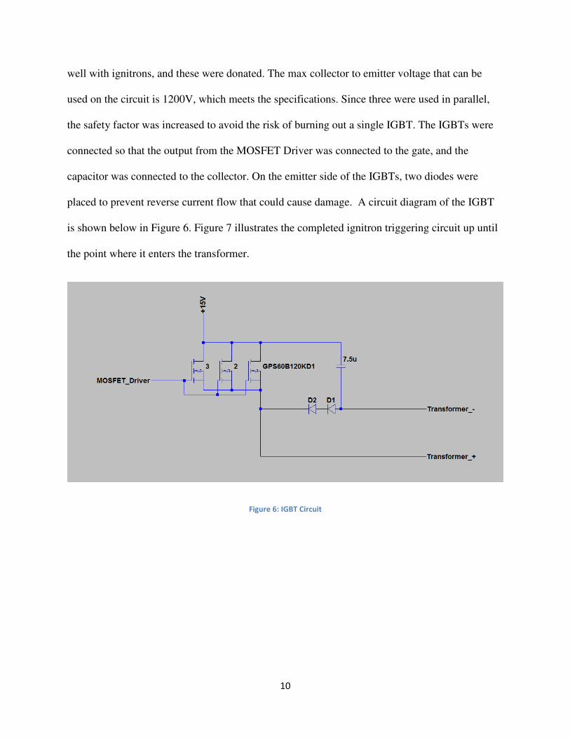
10
well with ignitrons, and these were donated. The max collector to emitter voltage that can be
used on the circuit is 1200V, which meets the specifications. Since three were used in parallel,
the safety factor was increased to avoid the risk of burning out a single IGBT. The IGBTs were
connected so that the output from the MOSFET Driver was connected to the gate, and the
capacitor was connected to the collector. On the emitter side of the IGBTs, two diodes were
placed to prevent reverse current flow that could cause damage. A circuit diagram of the IGBT
is shown below in Figure 6. Figure 7 illustrates the completed ignitron triggering circuit up until
the point where it enters the transformer.
Figure 6: IGBT Circuit

11

12

13
Figure 7: Current System with TTL Inverter, Monostable Multivibrator, MOSFET Driver, and IGBT

14
2.7 Transformer
While the triggering circuit up to this point gave a 1200V pulse, a pulse of at least 1500V
was needed to trigger each ignitron. In order to accomplish this, a transformer was used to step
up the voltage. This also allowed all four ignitrons to be driven from the one circuit by having
four secondary windings. The use of a transformer also allowed the ignitrons to be separated
from the rest of the circuit, so that a possible large current spike would not destroy all of the
components. The transformer is very useful, as the ignitron is dealing with thousands of amps,
and the triggering circuit is on the milliamp scale. Transformers need a varying current in order
to create a magnetic field, which is then converted back to a varying current on the secondary
winding. Since the ignitron triggering circuit deals with a pulse, the transformer is a perfect fit
for the application. Since we could not locate any wire that met our space and cost constraints,
we decided to make the windings ourselves. Wire was needed that could have thousands of volts
flowing through it with no sparking, and a combination of copper tape and kapton tape would
allow this. Kapton tape is used in space applications and has a breakdown voltage of over
4000V, which is more than what will be seen in any of the windings. Making the wire was also
an inexpensive way for us to get the length of wire needed. A 1:4 winding ratio was used for the
transformer, which would allow all four ignitrons to fire safely. The number of turns used was 10
for the primary winding, and 40 for each of the 4 secondary windings. Figure 8 shows an
LTSpice representation of the transformer, while Figure 9 is a photograph of the completed
transformer. Finally, Figure 10 presents the completed Ignitron Trigger Circuit.

15
Figure 8: Transformer Circuit
Figure 9: Picture of Completed Transformer

16

17

18
Figure 10: Completed Ignitron Trigger Circuit

19
2.8 Voltage Regulators
Three different voltage regulators were needed for the ignitron trigger circuit. In order to
accomplish this, three LM317s were used to regulate the voltage for each part of the circuit. The
formula that was used to calculate what values are needed for both R1 and R2 is:
1.25 1 !
1.25 "1 1 10330 $
1.251 3.03
1.254.03
5.04
The first voltage regulator is a 5V regulator that uses resistors with an R1 value of 330 Ω and an
R2 value of 1 kΩ. A 10 nF capacitor was also used going from the input to ground, to help with
the noise that was seen in the circuit. Since the input voltage is 24V, a heat sink was used to help
dissipate some of the heat that this configuration generated. The 5V regulator was used for the
TTL inverter circuit, along with the one-shot Monostable multivibrator. A circuit diagram of this
5V voltage regulator is shown in Figure 11 below.
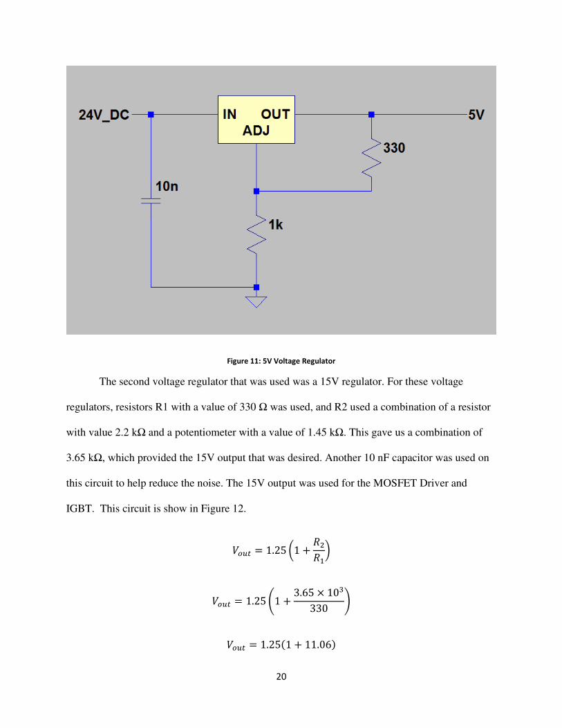
20
Figure 11: 5V Voltage Regulator
The second voltage regulator that was used was a 15V regulator. For these voltage
regulators, resistors R1 with a value of 330 Ω was used, and R2 used a combination of a resistor
with value 2.2 kΩ and a potentiometer with a value of 1.45 kΩ. This gave us a combination of
3.65 kΩ, which provided the 15V output that was desired. Another 10 nF capacitor was used on
this circuit to help reduce the noise. The 15V output was used for the MOSFET Driver and
IGBT. This circuit is show in Figure 12.
1.25 1 !
1.25 "1 3.65 10330 $
1.251 11.06

21
1.2512.06
15.08
Figure 12: 15V Voltage Regulator
The final voltage regulator that we needed to implement was built to charge the 7.5 µF
1200V capacitor, which is triggered through the IGBT to switch the ignitrons on. We needed to
drive an EMCO GP 15 DC to a DC converter. This would allow the voltage step-up, so that we
could charge the capacitor. Since the EMCO GP 15 is proportional between the input voltage and
output voltage, we decided to use two potentiometers to set the voltage regulator correctly, so
that we would not exceed the capacitor 1200V rating. As configured, R1 is equal to 240 Ω and
R2 is equal to 1.3 kΩ. This gives us an output to the DC to DC converter of 8.02 V. Two 10 nF
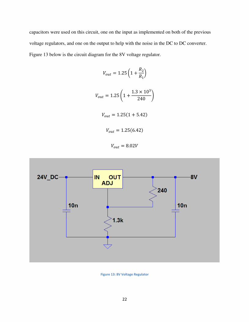
22
capacitors were used on this circuit, one on the input as implemented on both of the previous
voltage regulators, and one on the output to help with the noise in the DC to DC converter.
Figure 13 below is the circuit diagram for the 8V voltage regulator.
1.25 1 !
1.25 "1 1.3 10240 $
1.251 5.42
1.256.42
8.02
Figure 13: 8V Voltage Regulator

23
CHAPTER 3 – IMPLEMENTATION AND TESTING
3.1 Implementation
A modular approach was used in the construction of the circuit. When we built the TTL
Inverter we used a DC power supply to provide the power, and a function generator to accurately
measure the TTL output. The Monostable multivibrator was constructed similarly, using the
power supply and function generator to help build the circuit. All of these circuit blocks were
first assembled on a breadboard before implementation on a through-hole board. This allowed us
to very easily change resistance and capacitance values in the design of the circuits. In Figure 14,
you can see how the circuit was laid out on the breadboard. Once we had completed the testing
of the ignitron triggering circuit, we moved the circuit from a breadboard onto a through-hole
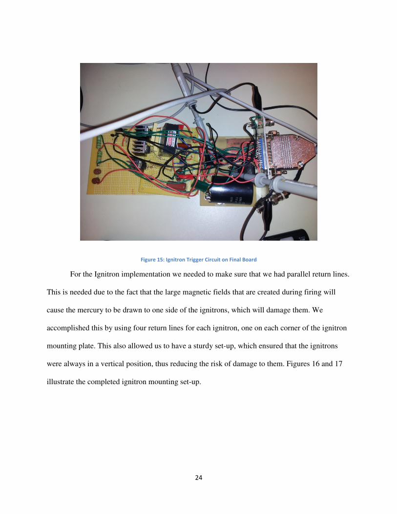
board which is shown in Figure 15.
Figure 14: Ignitron Trigger Circuit on Breadboard
24
Figure 15: Ignitron Trigger Circuit on Final Board
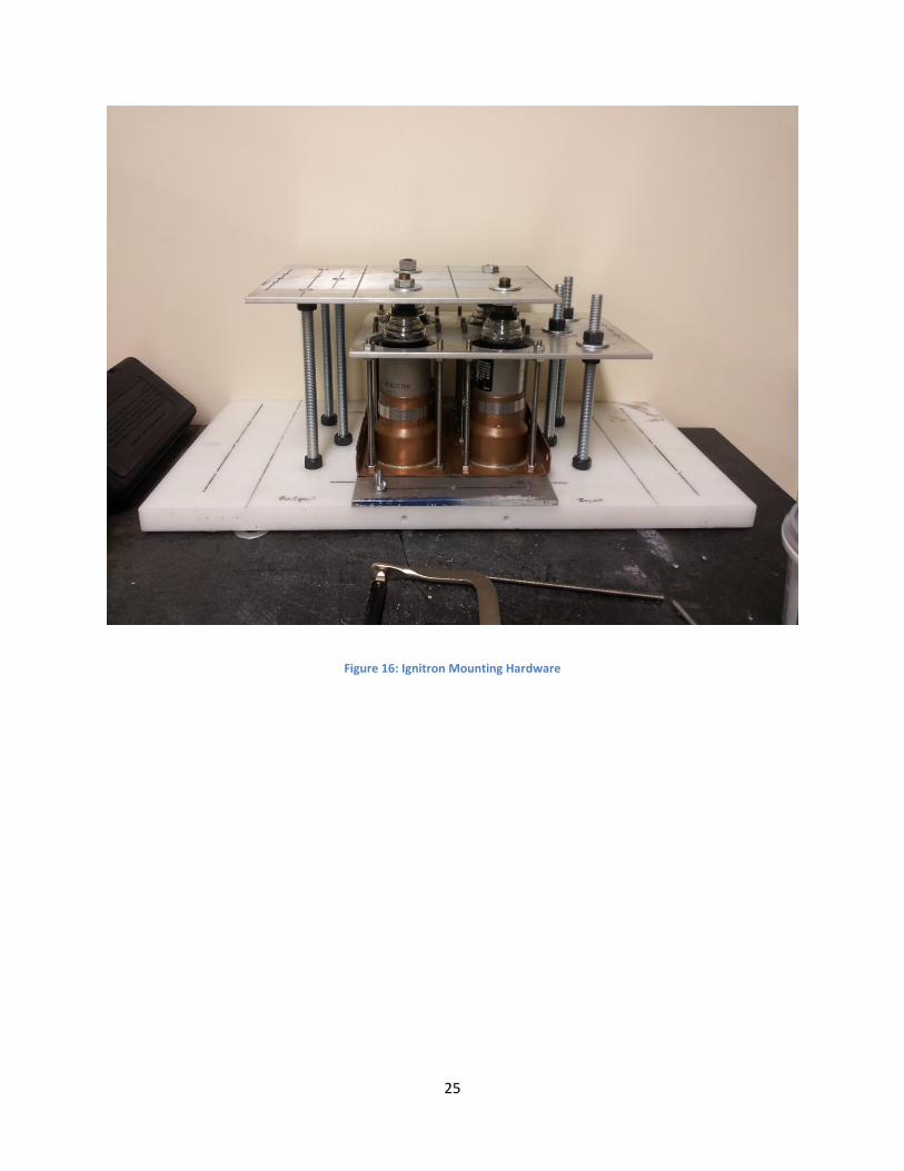
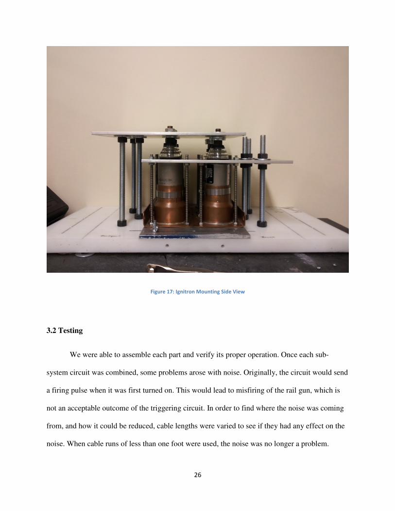
For the Ignitron implementation we needed to make sure that we had parallel return lines.
This is needed due to the fact that the large magnetic fields that are created during firing will
cause the mercury to be drawn to one side of the ignitrons, which will damage them. We
accomplished this by using four return lines for each ignitron, one on each corner of the ignitron
mounting plate. This also allowed us to have a sturdy set-up, which ensured that the ignitrons
were always in a vertical position, thus reducing the risk of damage to them. Figures 16 and 17
illustrate the completed ignitron mounting set-up.
25
Figure 16: Ignitron Mounting Hardware
26
Figure 17: Ignitron Mounting Side View
3.2 Testing
We were able to assemble each part and verify its proper operation. Once each sub-
system circuit was combined, some problems arose with noise. Originally, the circuit would send
a firing pulse when it was first turned on. This would lead to misfiring of the rail gun, which is
not an acceptable outcome of the triggering circuit. In order to find where the noise was coming
from, and how it could be reduced, cable lengths were varied to see if they had any effect on the
noise. When cable runs of less than one foot were used, the noise was no longer a problem.
27
During the actual firings of the rail gun, cable lengths of over 50 feet were used due to the fact
that the rail gun must be in a bunker, while the switch is in the control room. In order to account
for this, a 50 foot long cable was brought into the lab so that testing could be completed with an
accurate representation of the firing setup. In order to eliminate the noise, larger capacitors were
added in specific locations.
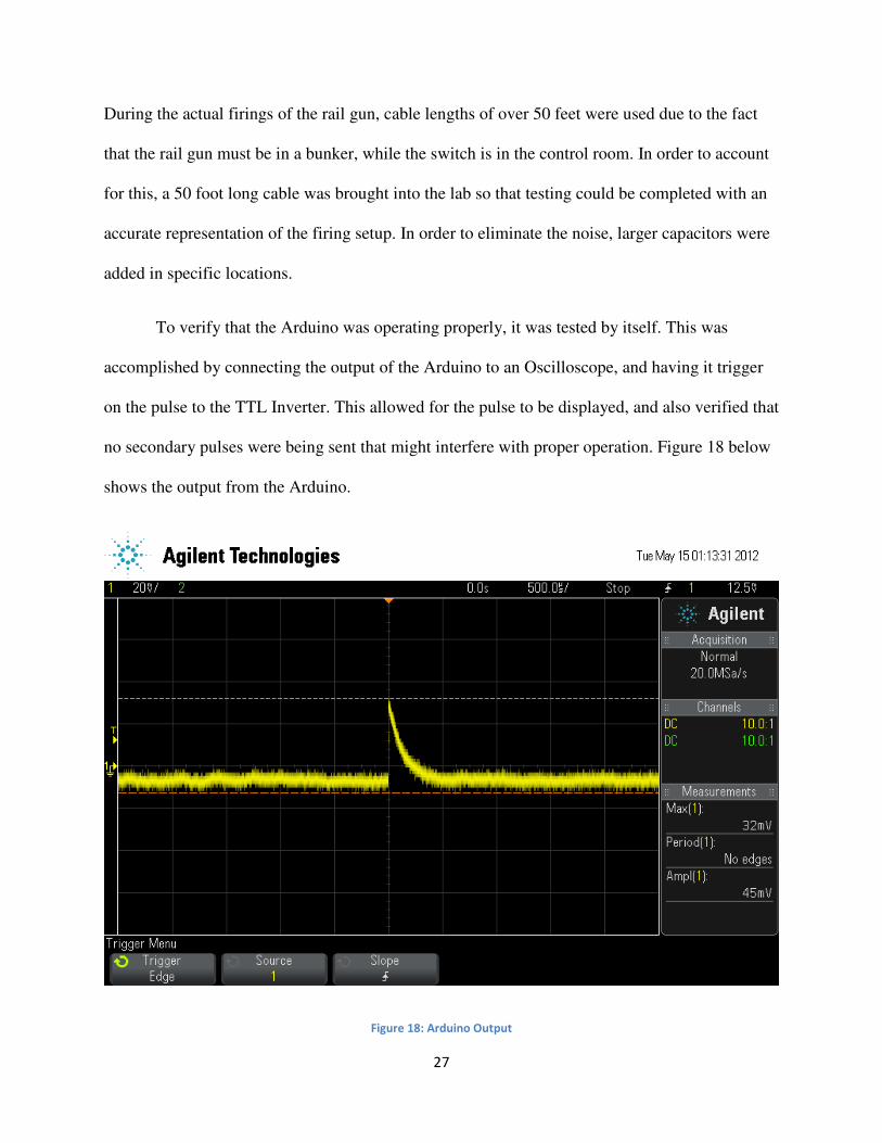
To verify that the Arduino was operating properly, it was tested by itself. This was
accomplished by connecting the output of the Arduino to an Oscilloscope, and having it trigger
on the pulse to the TTL Inverter. This allowed for the pulse to be displayed, and also verified that
no secondary pulses were being sent that might interfere with proper operation. Figure 18 below
shows the output from the Arduino.
Figure 18: Arduino Output
28
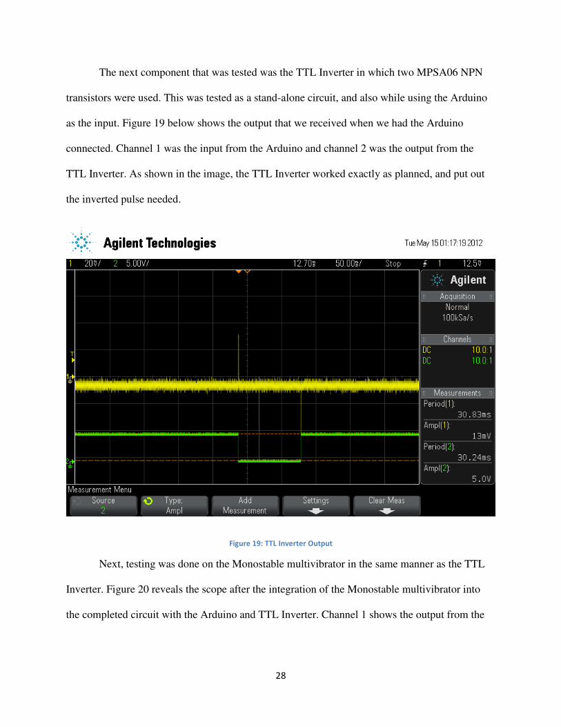
The next component that was tested was the TTL Inverter in which two MPSA06 NPN
transistors were used. This was tested as a stand-alone circuit, and also while using the Arduino
as the input. Figure 19 below shows the output that we received when we had the Arduino
connected. Channel 1 was the input from the Arduino and channel 2 was the output from the
TTL Inverter. As shown in the image, the TTL Inverter worked exactly as planned, and put out
the inverted pulse needed.
Figure 19: TTL Inverter Output
Next, testing was done on the Monostable multivibrator in the same manner as the TTL
Inverter. Figure 20 reveals the scope after the integration of the Monostable multivibrator into
the completed circuit with the Arduino and TTL Inverter. Channel 1 shows the output from the

29
TTL Inverter, which is the input to the Monostable multivibrator, and channel 2 shows the output
from the Monostable multivibrator.
Figure 20: Monostable Multivibrator Output
Since the circuit up to this point was working correctly, we decided to move on and test
the MIC5021 MOSFET Driver with the rest of the circuit. While the MOSFET Driver was
originally tested as a stand-alone chip, it was decided to test it along with the rest of the circuit so
that its proper operation could be verified. Figure 21 shows the image displayed on the
oscilloscope during testing. Channel 1 was the output from the Monostable multivibrator that
was used as the input for the MOSFET Driver, and channel 2 was the output from the MOSFET
Driver. As seen in the image below, the output was a 4 mS pulse with an amplitude of 14.9 V.

30
While the pulse length is a little bit shorter than was originally planned for, it is still much longer
than the 5 µS required to trigger the ignitrons.
Figure 21: MOSFET Driver Output
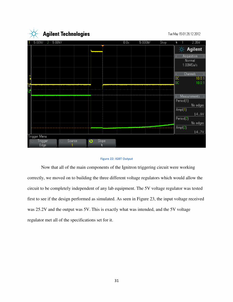
The next component tested was the IGBT. At this point, the ignitron triggering circuit
needed to be working correctly, as it is not possible to have a function generator supply the pulse
that is needed to correctly test the IGBTs. The first few tests that were completed were with the
capacitor uncharged, which allowed verification of the proper operation without having the
capacitor at 1000V. Figure 22 illustrates the result when the capacitor was uncharged. Channel 1
was the output from the MOSFET Driver that was used as the input for the IGBT and channel 2
was the output from the IGBT.
31
Figure 22: IGBT Output
Now that all of the main components of the Ignitron triggering circuit were working
correctly, we moved on to building the three different voltage regulators which would allow the
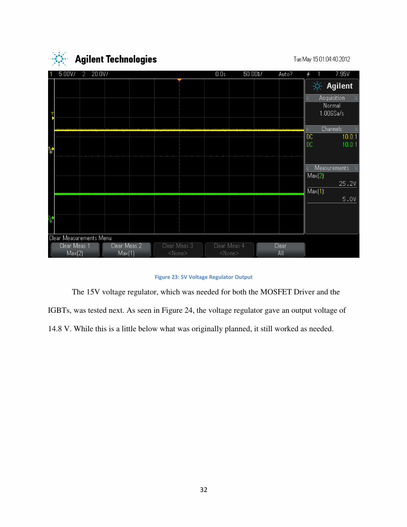
circuit to be completely independent of any lab equipment. The 5V voltage regulator was tested
first to see if the design performed as simulated. As seen in Figure 23, the input voltage received
was 25.2V and the output was 5V. This is exactly what was intended, and the 5V voltage
regulator met all of the specifications set for it.
32
Figure 23: 5V Voltage Regulator Output
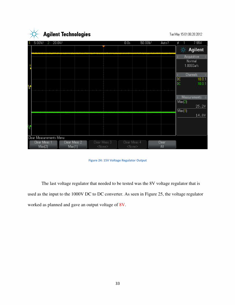
The 15V voltage regulator, which was needed for both the MOSFET Driver and the
IGBTs, was tested next. As seen in Figure 24, the voltage regulator gave an output voltage of
14.8 V. While this is a little below what was originally planned, it still worked as needed.
33
Figure 24: 15V Voltage Regulator Output
The last voltage regulator that needed to be tested was the 8V voltage regulator that is
used as the input to the 1000V DC to DC converter. As seen in Figure 25, the voltage regulator
worked as planned and gave an output voltage of 8V.

34
Figure 25: 8V Voltage Regulator Output
In order to test the transformer, we first checked the soldering job to ensure that it was
adequate, and then tested the continuity of each of the windings, to make sure the transformer
would work. Once this had been verified, we used a function generator to supply a sine wave at
60 Hz that would allow for verification that we had the correct turns ratio. Figure 26 shows how
the transformer worked when tested with a single winding. Channel 1 shows the input to the
primary winding and channel 2 shows the output from one of the secondary windings.
35
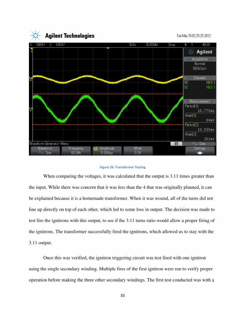
Figure 26: Transformer Testing
When comparing the voltages, it was calculated that the output is 3.11 times greater than
the input. While there was concern that it was less than the 4 that was originally planned, it can
be explained because it is a homemade transformer. When it was wound, all of the turns did not
line up directly on top of each other, which led to some loss in output. The decision was made to
test fire the ignitrons with this output, to see if the 3.11 turns ratio would allow a proper firing of
the ignitrons. The transformer successfully fired the ignitrons, which allowed us to stay with the
3.11 output.
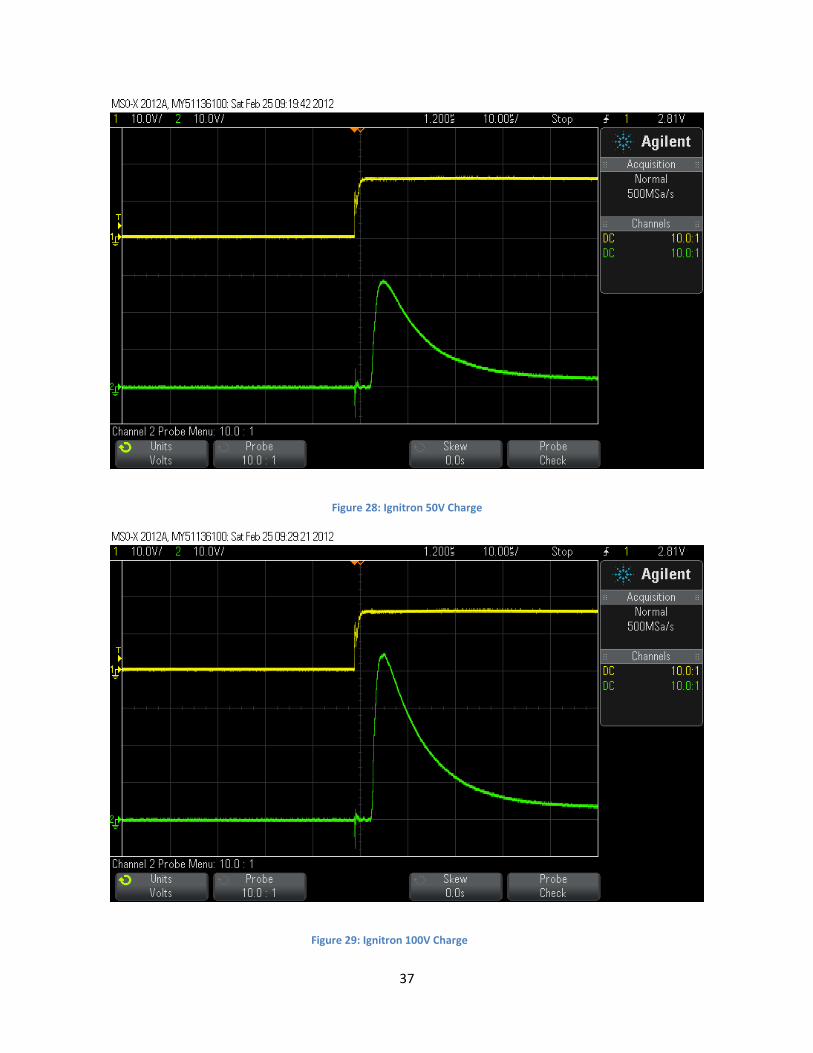
Once this was verified, the ignitron triggering circuit was test fired with one ignitron
using the single secondary winding. Multiple fires of the first ignitron were run to verify proper
operation before making the three other secondary windings. The first test conducted was with a

36
10V charge on the ignitron. The output from this test can be seen in Figure 27. Figure 28 reveals
what the output looked like when we ramped the charge voltage up to 50V, and Figure 29 shows
what it looked like with a 100V charge. On all three oscilloscope images, channel 1 shows the
pulse to trigger the ignitrons, and channel 2 is the output from the ignitrons.
Figure 27: Ignitron 10V Charge
37
Figure 28: Ignitron 50V Charge
Figure 29: Ignitron 100V Charge

38
CHAPTER 4 – CONCLUSION
After the testing was completed, it was determined that the Ignitron Trigger Circuit met
all of the requirements that were initially set for the project. The circuit succeeded in having a
4.5 mS pulse at around 3000V, which triggered all four of the Ignitrons. An additional test would
be to actually use the Ignitron Triggering Circuit on a full-voltage rail gun.
Now that the circuit has been built and tested, we can begin to modify the rail gun so that
we can ramp up the tests we are conducting. This will allow us to progress towards the goal of
firing at speeds representative of geosynchronous orbit.
The Ignitron Trigger Circuit can now be easily integrated with the compulsator being
developed by a group of Mechanical Engineering students, along with Electrical Engineering
student Bryan Bennett. Their developments will help to determine the direction we need to go, in
order to further improve the electromagnetic rail gun.

39
Bibliography
Data Sheets:
1. Fairchild Semiconductor MPSA06 NPN
2. Texas Instruments CH74HCT123E
3. International Rectifier IRGPS60B120KD
4. Micrel MIC5021
5. National Electronics NL7218H-100
6. Texas Instruments LM317
40
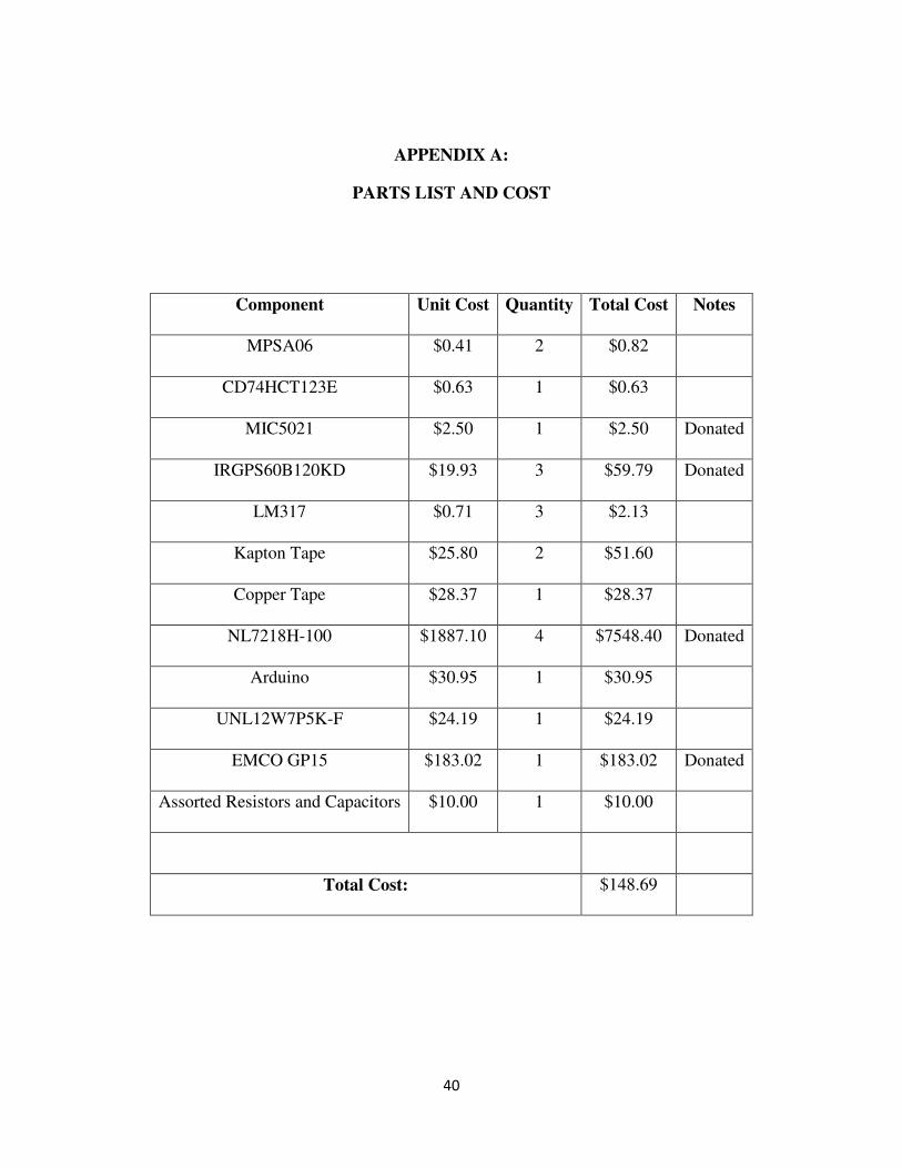
APPENDIX A:
PARTS LIST AND COST
Component Unit Cost Quantity Total Cost Notes
MPSA06 $0.41 2 $0.82
CD74HCT123E $0.63 1 $0.63
MIC5021 $2.50 1 $2.50 Donated
IRGPS60B120KD $19.93 3 $59.79 Donated
LM317 $0.71 3 $2.13
Kapton Tape $25.80 2 $51.60
Copper Tape $28.37 1 $28.37
NL7218H-100 $1887.10 4 $7548.40 Donated
Arduino $30.95 1 $30.95
UNL12W7P5K-F $24.19 1 $24.19
EMCO GP15 $183.02 1 $183.02 Donated
Assorted Resistors and Capacitors $10.00 1 $10.00
Total Cost: $148.69

41
APPENDIX B:
ARDUINO CODE
//All Code Written by Nolan Uchinizo
int ITC_trig = 12;
int button = 7;
int state = 0;
volatile int enable = LOW;
unsigned int count = 0;
unsigned long tmp = 0;
unsigned int oldSREG = 0;
void setup()
Serial.begin(9600);
pinMode(ITC_trig, OUTPUT);
pinMode(button, INPUT);
void loop()
switch (state)
case(0):
Serial.println("EMRG Mk.1 Firing Program.");
state = 1;
break;
case(1): //Initializes count, then jumps into the waiting state.
count = 0;
PORTB = B00000000;
enable = LOW;
state=2;
break;
case(2): //Waits for button press. If pressed, jumps to next
waiting state.
if(digitalRead(button) == HIGH)
PORTB |= B00011110;
state=3;
else
state = state;
break;
case(3):
delay(50);
state = 1;
break;