Embed Size (px)
Citation preview

IEEE TRANSACTIONS ON INDUSTRIAL ELECTRONICS, VOL. 57, NO. 10, OCTOBER 2010 1
A Universal Grid-Connected Fuel-Cell Inverter forResidential Application
Sudip K. Mazumder, Senior Member, IEEE, Rajni K. Burra, Member, IEEE, Rongjun Huang,Muhammad Tahir, Member, IEEE, and Kaustuva Acharya, Member, IEEE
Abstract—This paper describes a universal fuel-cell-based grid-connected inverter design with digital-signal-processor-based digi-tal control. The inverter has a direct power conversion mechanismwith a high-frequency zero-voltage-switched dc/ac primary-sideconverter followed by a pair of ac/ac cycloconverters that operateseither in parallel or in series to simultaneously address the issuesof universal output and high efficiency. The critical design issuesfocus on the impact and optimization of transformer leakageinductance with regard to effectiveness of zero voltage switchingof a primary-side converter, duty-cycle loss, resonance, and voltagespike that has effect on the breakdown voltage rating of the cyclo-converter devices. An additional concept of dynamic transformertapping has been explored to address the impact of varying inputvoltage on secondary-side voltage spike and inverter efficiency.Finally, detailed grid-parallel and grid-connected results are pre-sented that demonstrate satisfactory inverter performances.
Index Terms—AC/AC, control, dc/ac, digital signal processor(DSP), fuel cell, grid, high frequency, inverter, residential.
I. INTRODUCTION
THE utilization of fuel cells for distributed power gen-eration requires the development of a low-cost, high-
efficiency, and universal power-electronic system that convertsa fuel cell’s low-voltage output, which usually varies from 30 to60 V for residential application, into commercial 120-V/60-Hzand 240-V/50-Hz ac outputs [1]–[3]. In addition, the power-electronic system should have the following characteristics:1) output-voltage regulation for a wide variation in the outputvoltage of the fuel-cell stack; 2) capability for standaloneand grid-connected operations; 3) low output harmonics; and4) high energy-conversion efficiency.
Manuscript received August 25, 2008; revised December 30, 2008; acceptedMarch 4, 2009. This work was supported in part by the U.S. National ScienceFoundation under Awards 0725887 and 0239131 and in part by the U.S. Depart-ment of Energy under Award DE-FC2602NT41574. However, any opinions,findings, conclusions, or recommendations expressed herein are those of theauthors and do not necessarily reflect the views of the U.S. National ScienceFoundation or the U.S. Department of Energy.
S. K. Mazumder is with the Laboratory for Energy and Switching ElectronicsSystems, Department of Electrical and Computer Engineering, University ofIllinois at Chicago, Chicago, IL 60607 USA (e-mail: [email protected]).
R. K. Burra is with the GE Global Research Center, Bangalore 560 066, India(e-mail: [email protected]).
R. Huang is with International Rectifier, San Jose, CA 95134-1902 USA(e-mail: [email protected]).
M. Tahir is with the University of Engineering and Technology, Lahore54890, Pakistan (e-mail: [email protected]).
K. Acharya is with Texas Instruments Incorporated, Dallas, TX 75243 USA.Color versions of one or more of the figures in this paper are available online
at http://ieeexplore.ieee.org.Digital Object Identifier 10.1109/TIE.2009.2038943
Fig. 1. Power-conditioning scheme with (a) line-frequency transformer,(b) high-frequency transformer in the dc/ac stage [7], (c) high-frequencytransformer in the dc/dc stage [18], [19], and (d) single-stage isolated dc/acconverter [20].
Fig. 1(a)–(c) shows three mechanisms for achieving galvanicisolation between the fuel-cell stack and the application load.The conventional scheme, shown in Fig. 1(a), achieves isolationby placing a 50-Hz/60-Hz line-frequency transformer at theoutput of the inverter. Such a transformer is bulky because it hasto handle low-frequency currents and voltages. The other twooptions, shown in Fig. 1(b) and (c), achieve isolation by placingthe transformer within the power-conditioning system. Thehigh-frequency isolation can be included in the dc/ac converterstage, as shown in Fig. 1(b) [7], or in the dc/dc converterstage, as shown in Fig. 1(c) [18], [19]. Fig. 1(d) shows aneven more compact power-electronics option [20]. The single-stage isolated topology requires either a higher fuel-cell-stack
0278-0046/$26.00 © 2010 IEEE
2 IEEE TRANSACTIONS ON INDUSTRIAL ELECTRONICS, VOL. 57, NO. 10, OCTOBER 2010
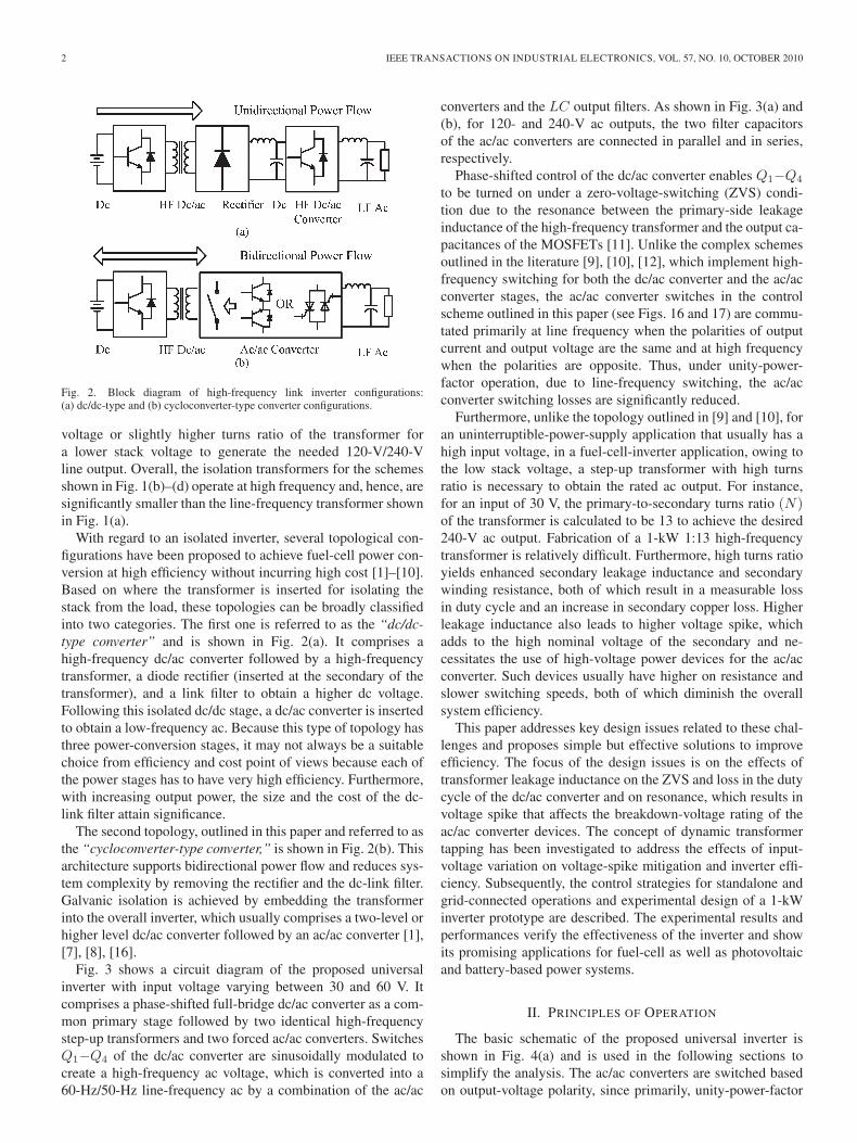
Fig. 2. Block diagram of high-frequency link inverter configurations:(a) dc/dc-type and (b) cycloconverter-type converter configurations.
voltage or slightly higher turns ratio of the transformer fora lower stack voltage to generate the needed 120-V/240-Vline output. Overall, the isolation transformers for the schemesshown in Fig. 1(b)–(d) operate at high frequency and, hence, aresignificantly smaller than the line-frequency transformer shownin Fig. 1(a).
With regard to an isolated inverter, several topological con-figurations have been proposed to achieve fuel-cell power con-version at high efficiency without incurring high cost [1]–[10].Based on where the transformer is inserted for isolating thestack from the load, these topologies can be broadly classifiedinto two categories. The first one is referred to as the “dc/dc-type converter” and is shown in Fig. 2(a). It comprises ahigh-frequency dc/ac converter followed by a high-frequencytransformer, a diode rectifier (inserted at the secondary of thetransformer), and a link filter to obtain a higher dc voltage.Following this isolated dc/dc stage, a dc/ac converter is insertedto obtain a low-frequency ac. Because this type of topology hasthree power-conversion stages, it may not always be a suitablechoice from efficiency and cost point of views because each ofthe power stages has to have very high efficiency. Furthermore,with increasing output power, the size and the cost of the dc-link filter attain significance.
The second topology, outlined in this paper and referred to asthe “cycloconverter-type converter,” is shown in Fig. 2(b). Thisarchitecture supports bidirectional power flow and reduces sys-tem complexity by removing the rectifier and the dc-link filter.Galvanic isolation is achieved by embedding the transformerinto the overall inverter, which usually comprises a two-level orhigher level dc/ac converter followed by an ac/ac converter [1],[7], [8], [16].
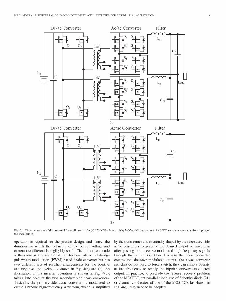
Fig. 3 shows a circuit diagram of the proposed universalinverter with input voltage varying between 30 and 60 V. Itcomprises a phase-shifted full-bridge dc/ac converter as a com-mon primary stage followed by two identical high-frequencystep-up transformers and two forced ac/ac converters. SwitchesQ1−Q4 of the dc/ac converter are sinusoidally modulated tocreate a high-frequency ac voltage, which is converted into a60-Hz/50-Hz line-frequency ac by a combination of the ac/ac
converters and the LC output filters. As shown in Fig. 3(a) and(b), for 120- and 240-V ac outputs, the two filter capacitorsof the ac/ac converters are connected in parallel and in series,respectively.
Phase-shifted control of the dc/ac converter enables Q1−Q4
to be turned on under a zero-voltage-switching (ZVS) condi-tion due to the resonance between the primary-side leakageinductance of the high-frequency transformer and the output ca-pacitances of the MOSFETs [11]. Unlike the complex schemesoutlined in the literature [9], [10], [12], which implement high-frequency switching for both the dc/ac converter and the ac/acconverter stages, the ac/ac converter switches in the controlscheme outlined in this paper (see Figs. 16 and 17) are commu-tated primarily at line frequency when the polarities of outputcurrent and output voltage are the same and at high frequencywhen the polarities are opposite. Thus, under unity-power-factor operation, due to line-frequency switching, the ac/acconverter switching losses are significantly reduced.
Furthermore, unlike the topology outlined in [9] and [10], foran uninterruptible-power-supply application that usually has ahigh input voltage, in a fuel-cell-inverter application, owing tothe low stack voltage, a step-up transformer with high turnsratio is necessary to obtain the rated ac output. For instance,for an input of 30 V, the primary-to-secondary turns ratio (N)of the transformer is calculated to be 13 to achieve the desired240-V ac output. Fabrication of a 1-kW 1:13 high-frequencytransformer is relatively difficult. Furthermore, high turns ratioyields enhanced secondary leakage inductance and secondarywinding resistance, both of which result in a measurable lossin duty cycle and an increase in secondary copper loss. Higherleakage inductance also leads to higher voltage spike, whichadds to the high nominal voltage of the secondary and ne-cessitates the use of high-voltage power devices for the ac/acconverter. Such devices usually have higher on resistance andslower switching speeds, both of which diminish the overallsystem efficiency.
This paper addresses key design issues related to these chal-lenges and proposes simple but effective solutions to improveefficiency. The focus of the design issues is on the effects oftransformer leakage inductance on the ZVS and loss in the dutycycle of the dc/ac converter and on resonance, which results involtage spike that affects the breakdown-voltage rating of theac/ac converter devices. The concept of dynamic transformertapping has been investigated to address the effects of input-voltage variation on voltage-spike mitigation and inverter effi-ciency. Subsequently, the control strategies for standalone andgrid-connected operations and experimental design of a 1-kWinverter prototype are described. The experimental results andperformances verify the effectiveness of the inverter and showits promising applications for fuel-cell as well as photovoltaicand battery-based power systems.
II. PRINCIPLES OF OPERATION
The basic schematic of the proposed universal inverter isshown in Fig. 4(a) and is used in the following sections tosimplify the analysis. The ac/ac converters are switched basedon output-voltage polarity, since primarily, unity-power-factor

MAZUMDER et al.: UNIVERSAL GRID-CONNECTED FUEL-CELL INVERTER FOR RESIDENTIAL APPLICATION 3
Fig. 3. Circuit diagrams of the proposed fuel-cell inverter for (a) 120-V/60-Hz ac and (b) 240-V/50-Hz ac outputs. An SPDT switch enables adaptive tapping ofthe transformer.
operation is required for the present design, and hence, theduration for which the polarities of the output voltage andcurrent are different is negligibly small. The circuit schematicis the same as a conventional transformer-isolated full-bridgepulsewidth-modulation (PWM)-based dc/dc converter but hastwo different sets of rectifier arrangements for the positiveand negative line cycles, as shown in Fig. 4(b) and (c). Anillustration of the inverter operation is shown in Fig. 4(d),taking into account the two secondary-side ac/ac converters.Basically, the primary-side dc/ac converter is modulated tocreate a bipolar high-frequency waveform, which is amplified
by the transformer and eventually shaped by the secondary-sideac/ac converters to generate the desired output ac waveformafter passing the sinewave-modulated high-frequency signalsthrough the output LC filter. Because the dc/ac convertercreates the sinewave-modulated output, the ac/ac converterswitches do not need to force switch; they can simply operateat line frequency to rectify the bipolar sinewave-modulatedoutput. In practice, to preclude the reverse-recovery problemof the MOSFET, antiparallel diode, use of Schottky diode [21]or channel conduction of one of the MOSFETs [as shown inFig. 4(d)] may need to be adopted.
4 IEEE TRANSACTIONS ON INDUSTRIAL ELECTRONICS, VOL. 57, NO. 10, OCTOBER 2010
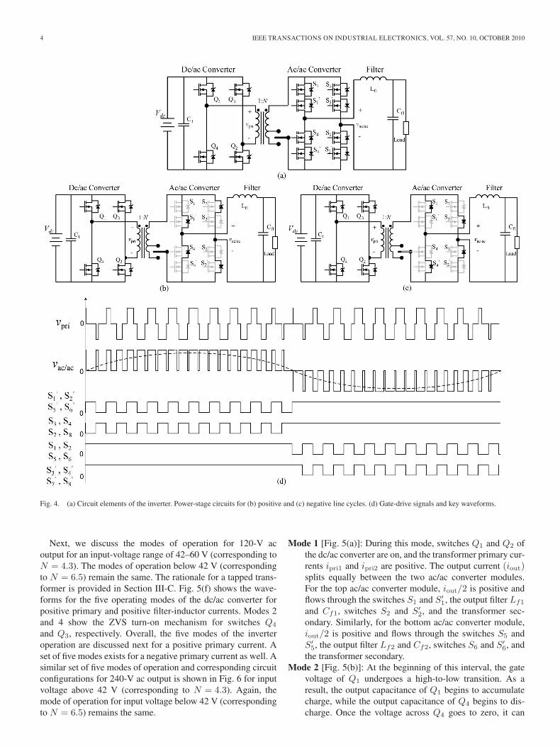
Fig. 4. (a) Circuit elements of the inverter. Power-stage circuits for (b) positive and (c) negative line cycles. (d) Gate-drive signals and key waveforms.
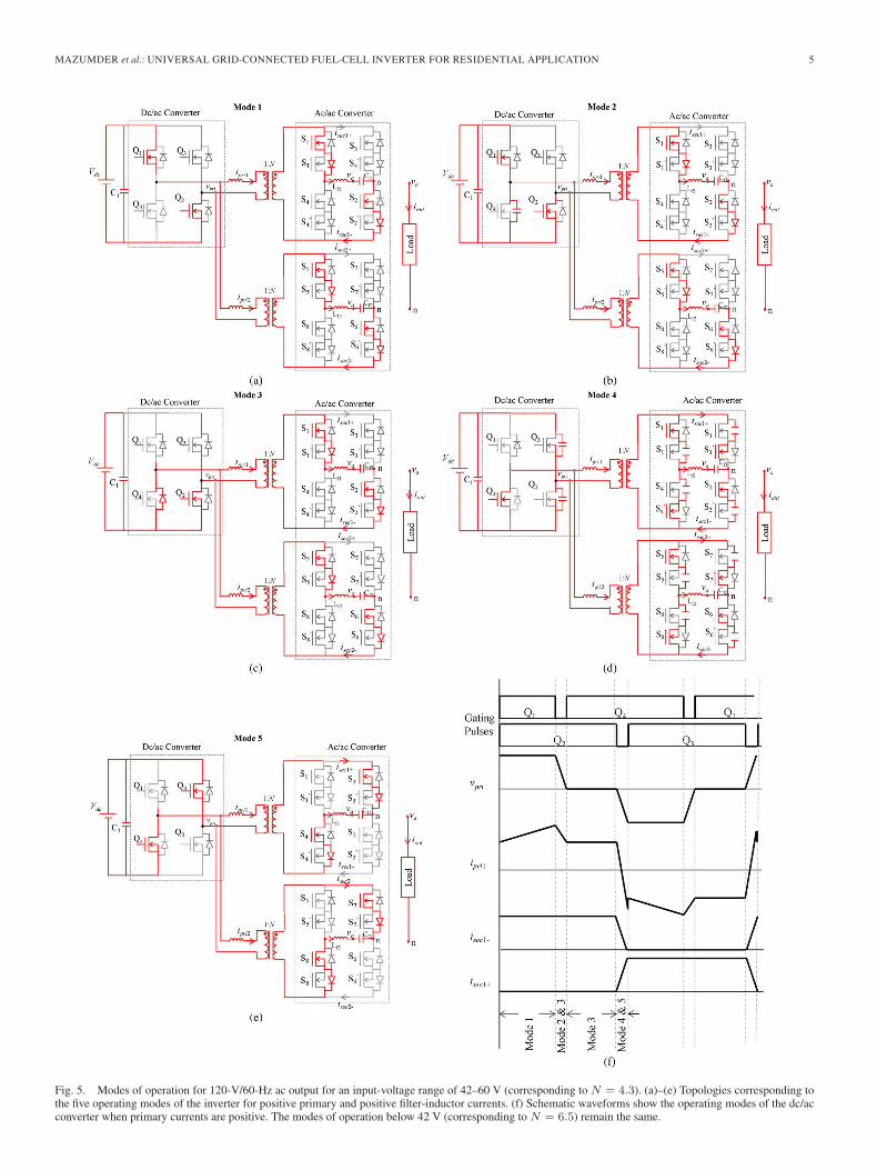
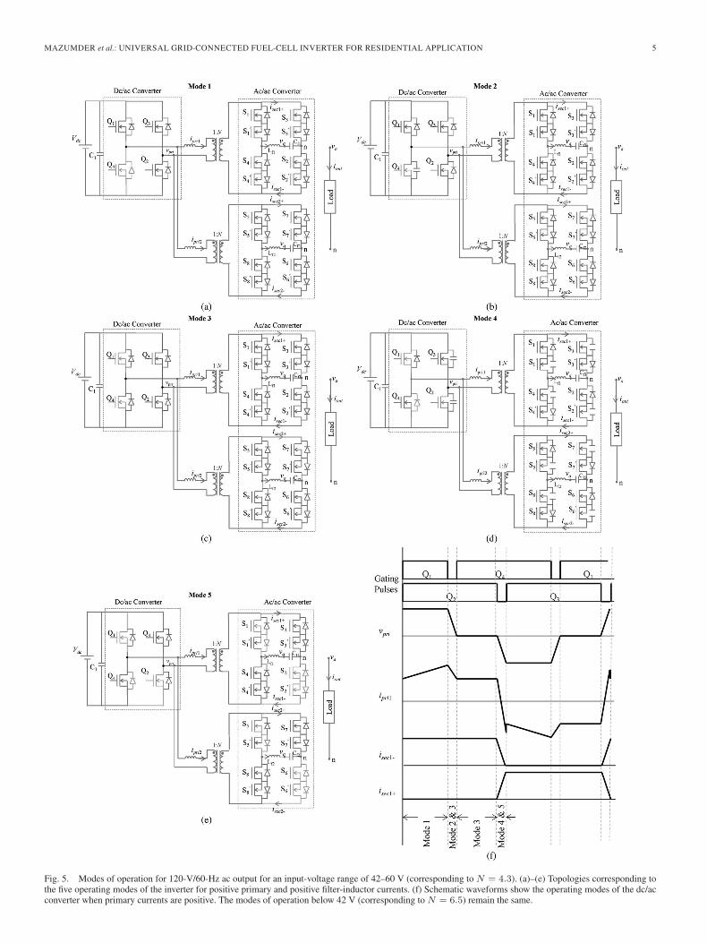
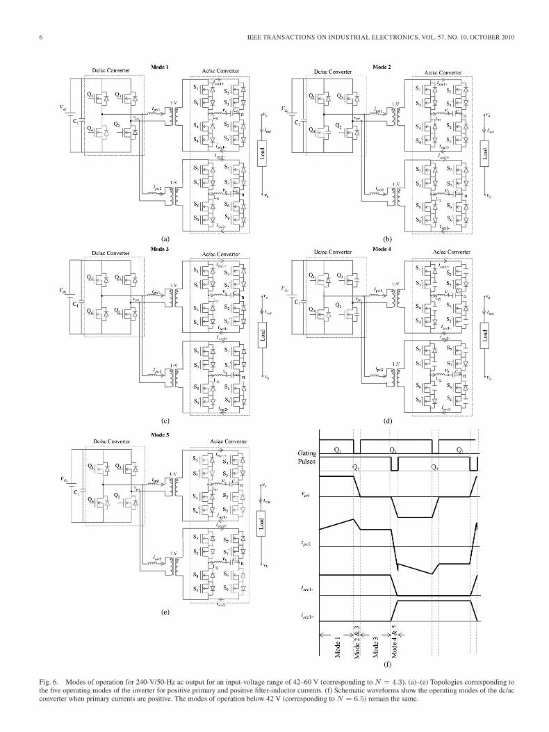
Next, we discuss the modes of operation for 120-V acoutput for an input-voltage range of 42–60 V (corresponding toN = 4.3). The modes of operation below 42 V (correspondingto N = 6.5) remain the same. The rationale for a tapped trans-former is provided in Section III-C. Fig. 5(f) shows the wave-forms for the five operating modes of the dc/ac converter forpositive primary and positive filter-inductor currents. Modes 2and 4 show the ZVS turn-on mechanism for switches Q4
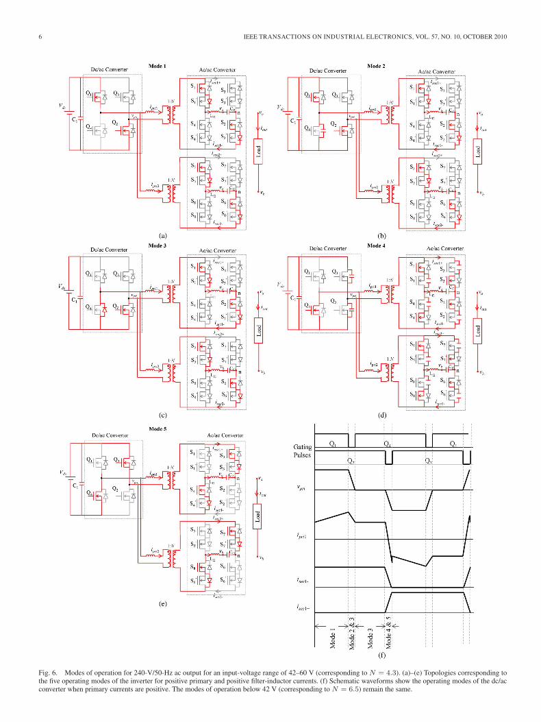
and Q3, respectively. Overall, the five modes of the inverteroperation are discussed next for a positive primary current. Aset of five modes exists for a negative primary current as well. Asimilar set of five modes of operation and corresponding circuitconfigurations for 240-V ac output is shown in Fig. 6 for inputvoltage above 42 V (corresponding to N = 4.3). Again, themode of operation for input voltage below 42 V (correspondingto N = 6.5) remains the same.
Mode 1 [Fig. 5(a)]: During this mode, switches Q1 and Q2 ofthe dc/ac converter are on, and the transformer primary cur-rents ipri1 and ipri2 are positive. The output current (iout)splits equally between the two ac/ac converter modules.For the top ac/ac converter module, iout/2 is positive andflows through the switches S1 and S ′
1, the output filter Lf1
and Cf1, switches S2 and S ′2, and the transformer sec-
ondary. Similarly, for the bottom ac/ac converter module,iout/2 is positive and flows through the switches S5 andS ′
5, the output filter Lf2 and Cf2, switches S6 and S ′6, and
the transformer secondary.Mode 2 [Fig. 5(b)]: At the beginning of this interval, the gate
voltage of Q1 undergoes a high-to-low transition. As aresult, the output capacitance of Q1 begins to accumulatecharge, while the output capacitance of Q4 begins to dis-charge. Once the voltage across Q4 goes to zero, it can
MAZUMDER et al.: UNIVERSAL GRID-CONNECTED FUEL-CELL INVERTER FOR RESIDENTIAL APPLICATION 5
Fig. 5. Modes of operation for 120-V/60-Hz ac output for an input-voltage range of 42–60 V (corresponding to N = 4.3). (a)–(e) Topologies corresponding tothe five operating modes of the inverter for positive primary and positive filter-inductor currents. (f) Schematic waveforms show the operating modes of the dc/acconverter when primary currents are positive. The modes of operation below 42 V (corresponding to N = 6.5) remain the same.
6 IEEE TRANSACTIONS ON INDUSTRIAL ELECTRONICS, VOL. 57, NO. 10, OCTOBER 2010
Fig. 6. Modes of operation for 240-V/50-Hz ac output for an input-voltage range of 42–60 V (corresponding to N = 4.3). (a)–(e) Topologies corresponding tothe five operating modes of the inverter for positive primary and positive filter-inductor currents. (f) Schematic waveforms show the operating modes of the dc/acconverter when primary currents are positive. The modes of operation below 42 V (corresponding to N = 6.5) remain the same.

MAZUMDER et al.: UNIVERSAL GRID-CONNECTED FUEL-CELL INVERTER FOR RESIDENTIAL APPLICATION 7
be turned on under ZVS. The transformer primary currentsipri1 and ipri2 and the load current iout continue to flow inthe same direction.
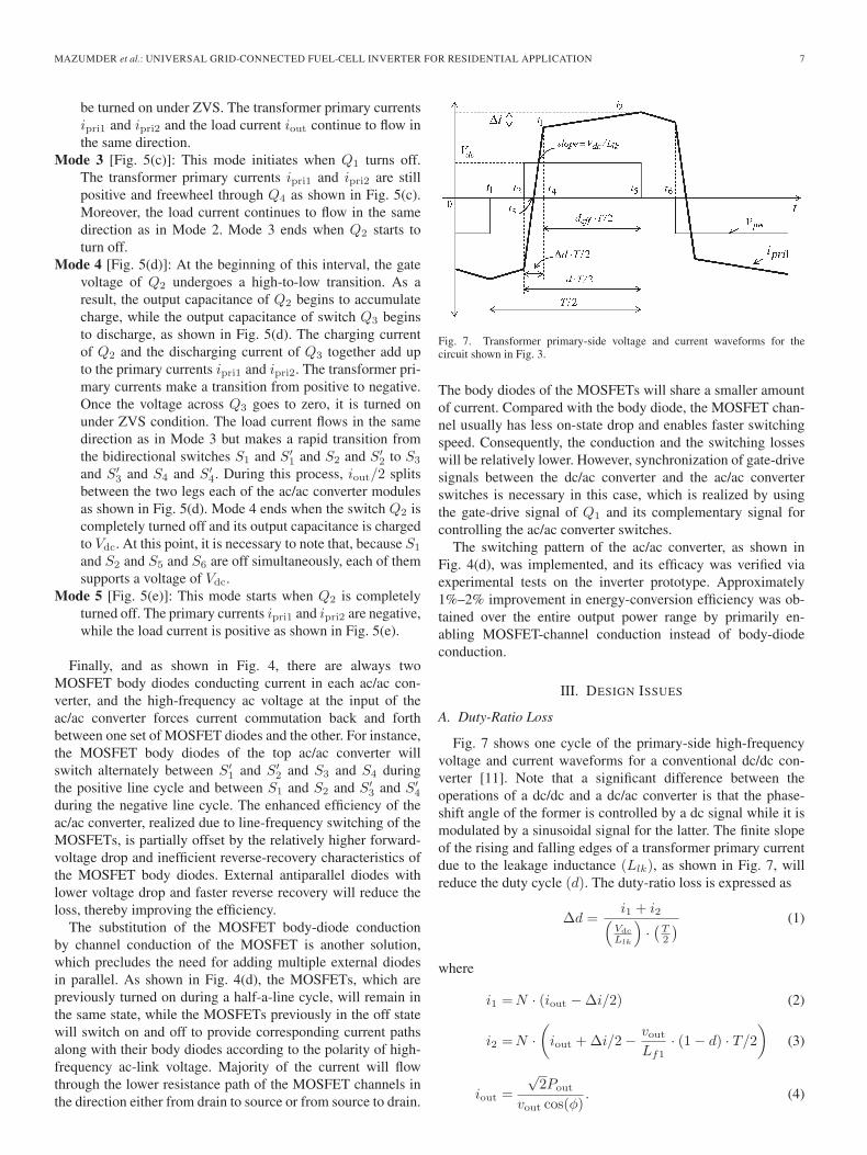
Mode 3 [Fig. 5(c)]: This mode initiates when Q1 turns off.The transformer primary currents ipri1 and ipri2 are stillpositive and freewheel through Q4 as shown in Fig. 5(c).Moreover, the load current continues to flow in the samedirection as in Mode 2. Mode 3 ends when Q2 starts toturn off.
Mode 4 [Fig. 5(d)]: At the beginning of this interval, the gatevoltage of Q2 undergoes a high-to-low transition. As aresult, the output capacitance of Q2 begins to accumulatecharge, while the output capacitance of switch Q3 beginsto discharge, as shown in Fig. 5(d). The charging currentof Q2 and the discharging current of Q3 together add upto the primary currents ipri1 and ipri2. The transformer pri-mary currents make a transition from positive to negative.Once the voltage across Q3 goes to zero, it is turned onunder ZVS condition. The load current flows in the samedirection as in Mode 3 but makes a rapid transition fromthe bidirectional switches S1 and S ′
1 and S2 and S ′2 to S3
and S ′3 and S4 and S ′
4. During this process, iout/2 splitsbetween the two legs each of the ac/ac converter modulesas shown in Fig. 5(d). Mode 4 ends when the switch Q2 iscompletely turned off and its output capacitance is chargedto Vdc. At this point, it is necessary to note that, because S1
and S2 and S5 and S6 are off simultaneously, each of themsupports a voltage of Vdc.
Mode 5 [Fig. 5(e)]: This mode starts when Q2 is completelyturned off. The primary currents ipri1 and ipri2 are negative,while the load current is positive as shown in Fig. 5(e).
Finally, and as shown in Fig. 4, there are always twoMOSFET body diodes conducting current in each ac/ac con-verter, and the high-frequency ac voltage at the input of theac/ac converter forces current commutation back and forthbetween one set of MOSFET diodes and the other. For instance,the MOSFET body diodes of the top ac/ac converter willswitch alternately between S ′
1 and S ′2 and S3 and S4 during
the positive line cycle and between S1 and S2 and S ′3 and S ′
4
during the negative line cycle. The enhanced efficiency of theac/ac converter, realized due to line-frequency switching of theMOSFETs, is partially offset by the relatively higher forward-voltage drop and inefficient reverse-recovery characteristics ofthe MOSFET body diodes. External antiparallel diodes withlower voltage drop and faster reverse recovery will reduce theloss, thereby improving the efficiency.
The substitution of the MOSFET body-diode conductionby channel conduction of the MOSFET is another solution,which precludes the need for adding multiple external diodesin parallel. As shown in Fig. 4(d), the MOSFETs, which arepreviously turned on during a half-a-line cycle, will remain inthe same state, while the MOSFETs previously in the off statewill switch on and off to provide corresponding current pathsalong with their body diodes according to the polarity of high-frequency ac-link voltage. Majority of the current will flowthrough the lower resistance path of the MOSFET channels inthe direction either from drain to source or from source to drain.
Fig. 7. Transformer primary-side voltage and current waveforms for thecircuit shown in Fig. 3.
The body diodes of the MOSFETs will share a smaller amountof current. Compared with the body diode, the MOSFET chan-nel usually has less on-state drop and enables faster switchingspeed. Consequently, the conduction and the switching losseswill be relatively lower. However, synchronization of gate-drivesignals between the dc/ac converter and the ac/ac converterswitches is necessary in this case, which is realized by usingthe gate-drive signal of Q1 and its complementary signal forcontrolling the ac/ac converter switches.
The switching pattern of the ac/ac converter, as shown inFig. 4(d), was implemented, and its efficacy was verified viaexperimental tests on the inverter prototype. Approximately1%–2% improvement in energy-conversion efficiency was ob-tained over the entire output power range by primarily en-abling MOSFET-channel conduction instead of body-diodeconduction.
III. DESIGN ISSUES
A. Duty-Ratio Loss
Fig. 7 shows one cycle of the primary-side high-frequencyvoltage and current waveforms for a conventional dc/dc con-verter [11]. Note that a significant difference between theoperations of a dc/dc and a dc/ac converter is that the phase-shift angle of the former is controlled by a dc signal while it ismodulated by a sinusoidal signal for the latter. The finite slopeof the rising and falling edges of a transformer primary currentdue to the leakage inductance (Llk), as shown in Fig. 7, willreduce the duty cycle (d). The duty-ratio loss is expressed as
Δd =i1 + i2(
VdcLlk
)·(
T2
) (1)
where
i1 =N · (iout − Δi/2) (2)
i2 =N ·(
iout + Δi/2 − vout
Lf1· (1 − d) · T/2
)(3)
iout =√
2Pout
vout cos(φ). (4)
8 IEEE TRANSACTIONS ON INDUSTRIAL ELECTRONICS, VOL. 57, NO. 10, OCTOBER 2010
Fig. 8. Variation of the duty-ratio loss as a function of the leakage inductanceof the transformer over the half-a-line cycle.
TABLE ICONDUCTING COMPONENTS AT DIFFERENT INTERVALS FOR
THE CIRCUIT SHOWN IN FIG. 4(a). DIODES D1−D4
ARE ANTIPARALLEL DIODES OF Q1−Q4
In (2) and (3), N is the transformer turns ratio, Lf1 is the outputfilter inductance, iout is the filter current, vout is the outputvoltage, T is the switching period, Δi is the filter inductorcurrent ripple, Pout is the output power, and cos(φ) is the loadpower factor. By substituting (2) and (3) into (1), we obtain
Δd =N
VdcLlk
· T2
·(
2iout −vout
Lf1· (1 − d) · T
2
). (5)
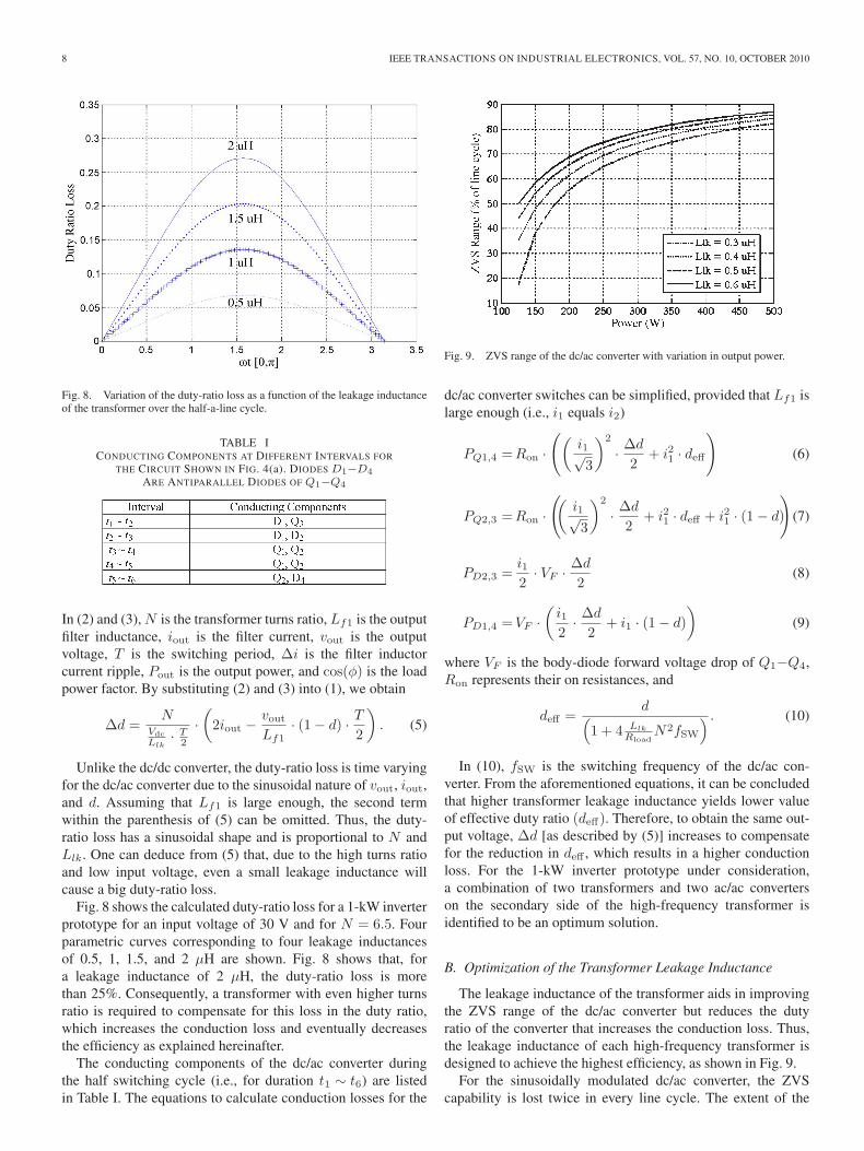
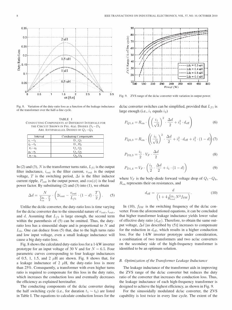
Unlike the dc/dc converter, the duty-ratio loss is time varyingfor the dc/ac converter due to the sinusoidal nature of vout, iout,and d. Assuming that Lf1 is large enough, the second termwithin the parenthesis of (5) can be omitted. Thus, the duty-ratio loss has a sinusoidal shape and is proportional to N andLlk. One can deduce from (5) that, due to the high turns ratioand low input voltage, even a small leakage inductance willcause a big duty-ratio loss.
Fig. 8 shows the calculated duty-ratio loss for a 1-kW inverterprototype for an input voltage of 30 V and for N = 6.5. Fourparametric curves corresponding to four leakage inductancesof 0.5, 1, 1.5, and 2 μH are shown. Fig. 8 shows that, fora leakage inductance of 2 μH, the duty-ratio loss is morethan 25%. Consequently, a transformer with even higher turnsratio is required to compensate for this loss in the duty ratio,which increases the conduction loss and eventually decreasesthe efficiency as explained hereinafter.
The conducting components of the dc/ac converter duringthe half switching cycle (i.e., for duration t1 ∼ t6) are listedin Table I. The equations to calculate conduction losses for the
Fig. 9. ZVS range of the dc/ac converter with variation in output power.
dc/ac converter switches can be simplified, provided that Lf1 islarge enough (i.e., i1 equals i2)
PQ1,4 = Ron ·((
i1√3
)2
· Δd
2+ i21 · deff
)(6)
PQ2,3 = Ron ·((
i1√3
)2
· Δd
2+ i21 · deff + i21 · (1 − d)
)(7)
PD2,3 =i12· VF · Δd
2(8)
PD1,4 = VF ·(
i12· Δd
2+ i1 · (1 − d)
)(9)
where VF is the body-diode forward voltage drop of Q1−Q4,Ron represents their on resistances, and
deff =d(
1 + 4 Llk
RloadN2fSW
) . (10)
In (10), fSW is the switching frequency of the dc/ac con-verter. From the aforementioned equations, it can be concludedthat higher transformer leakage inductance yields lower valueof effective duty ratio (deff). Therefore, to obtain the same out-put voltage, Δd [as described by (5)] increases to compensatefor the reduction in deff , which results in a higher conductionloss. For the 1-kW inverter prototype under consideration,a combination of two transformers and two ac/ac converterson the secondary side of the high-frequency transformer isidentified to be an optimum solution.
B. Optimization of the Transformer Leakage Inductance
The leakage inductance of the transformer aids in improvingthe ZVS range of the dc/ac converter but reduces the dutyratio of the converter that increases the conduction loss. Thus,the leakage inductance of each high-frequency transformer isdesigned to achieve the highest efficiency, as shown in Fig. 9.
For the sinusoidally modulated dc/ac converter, the ZVScapability is lost twice in every line cycle. The extent of the
MAZUMDER et al.: UNIVERSAL GRID-CONNECTED FUEL-CELL INVERTER FOR RESIDENTIAL APPLICATION 9
loss of ZVS is a function of the output current. The availableZVS range (tZVS) as a percentage of the line cycle (tLineCycle)is given by
tZVS
tLineCycle=
2π
sin−1
(14
V 2dc
(43Coss + 1
2CT
)i2outLlk
) 12
(11)
where Coss is the device output capacitance and CT is theinterwinding capacitance of the transformer. When the dc/acconverter is not operating under ZVS condition, the devicesare hard switched. In steady state, the switching loss (PSW) ofeach MOSFET during hard switching depends on the switchingfrequency and the gate resistance (RGATE) and is given by
PSW =Vdciout sin(ωt)
2fSW
(tS(L→H) + tS(H→L)
)(12)
where ω is the line frequency in radians per second and the low-to-high and high-to-low transition times (tS(L→H) and tS(H→L))are given by
tS(L→H) =QG(SW)RGATE
VDD − VSPtS(H→L) =
QG(SW)RGATE
VSP.
(13)
In (13), QG(SW) is the gate charge, VDD is the bias voltageof the gate driver, VSP is the source voltage, and RGATE is thegate resistance. The conduction loss of the MOSFET in steadystate is described using
Pcond1,3 =Ron
[(i1 sin(ωt)√
3
)2 Δd
2+ i2out sin2(ωt)deff
]
(14)
Pcond2,4 =Ron
[ (i1 sin(ωt)√
3
)2 Δd
2+ i2out sin2(ωt)deff
+ i21 sin2(ωt)(1 − d)
]. (15)
To optimize the leakage inductance, the total loss of the dc/acconverter over the half-a-line cycle has to be estimated, and itis determined using
Pdevice =1π
π/ω∫0
(2Pcond1,3+2Pcond2,4+2PSW
tZVS
tLineCycle
)dt.
(16)
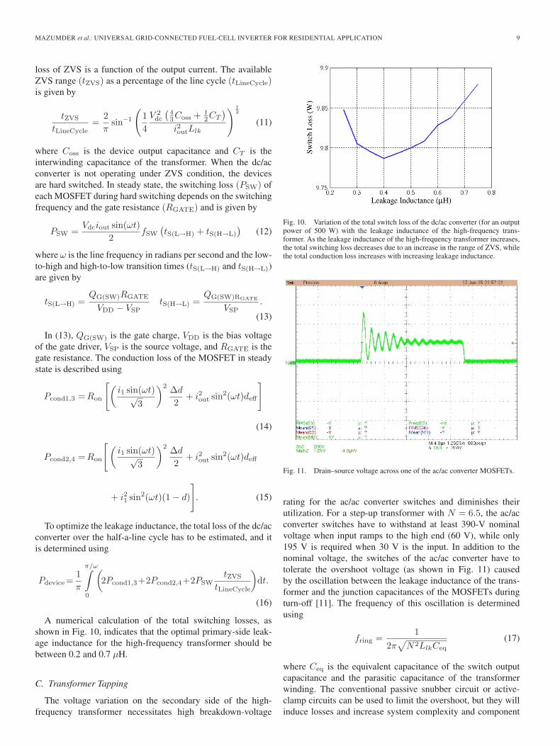
A numerical calculation of the total switching losses, asshown in Fig. 10, indicates that the optimal primary-side leak-age inductance for the high-frequency transformer should bebetween 0.2 and 0.7 μH.
C. Transformer Tapping
The voltage variation on the secondary side of the high-frequency transformer necessitates high breakdown-voltage
Fig. 10. Variation of the total switch loss of the dc/ac converter (for an outputpower of 500 W) with the leakage inductance of the high-frequency trans-former. As the leakage inductance of the high-frequency transformer increases,the total switching loss decreases due to an increase in the range of ZVS, whilethe total conduction loss increases with increasing leakage inductance.
Fig. 11. Drain–source voltage across one of the ac/ac converter MOSFETs.
rating for the ac/ac converter switches and diminishes theirutilization. For a step-up transformer with N = 6.5, the ac/acconverter switches have to withstand at least 390-V nominalvoltage when input ramps to the high end (60 V), while only195 V is required when 30 V is the input. In addition to thenominal voltage, the switches of the ac/ac converter have totolerate the overshoot voltage (as shown in Fig. 11) causedby the oscillation between the leakage inductance of the trans-former and the junction capacitances of the MOSFETs duringturn-off [11]. The frequency of this oscillation is determinedusing
fring =1
2π√
N2LlkCeq
(17)
where Ceq is the equivalent capacitance of the switch outputcapacitance and the parasitic capacitance of the transformerwinding. The conventional passive snubber circuit or active-clamp circuits can be used to limit the overshoot, but they willinduce losses and increase system complexity and component
10 IEEE TRANSACTIONS ON INDUSTRIAL ELECTRONICS, VOL. 57, NO. 10, OCTOBER 2010
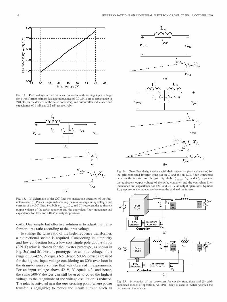
Fig. 12. Peak voltage across the ac/ac converter with varying input voltagefor a transformer primary leakage inductance of 0.7 μH, output capacitance of240 pF (for the devices of the ac/ac converter), and output filter inductance andcapacitance of 1 mH and 2.2 μF, respectively.
Fig. 13. (a) Schematic of the LC filter for standalone operation of the fuel-cell inverter. (b) Phasor diagram describing the relationship among voltages andcurrents of the LC filter. Symbols v′
ac/ac, L′
f , and C′f represent the equivalent
output voltage of the ac/ac converter and the equivalent filter inductance andcapacitance for 120- and 240-V ac output operations.
costs. One simple but effective solution is to adjust the trans-former turns ratio according to the input voltage.
To change the turns ratio of the high-frequency transformer,a bidirectional switch is required. Considering its simplicityand low conduction loss, a low-cost single-pole-double-throw(SPDT) relay is chosen for the inverter prototype, as shown inFig. 3(a) and (b). For this prototype, for an input voltage in therange of 30–42 V, N equals 6.5. Hence, 500-V devices are usedfor the highest input voltage considering an 80% overshoot inthe drain-to-source voltage that was observed in experiments.For an input voltage above 42 V, N equals 4.3, and hence,the same 500-V devices can still be used to cover the highestvoltage as the magnitude of the voltage oscillation is reduced.The relay is activated near the zero-crossing point (where powertransfer is negligible) to reduce the inrush current. Such an
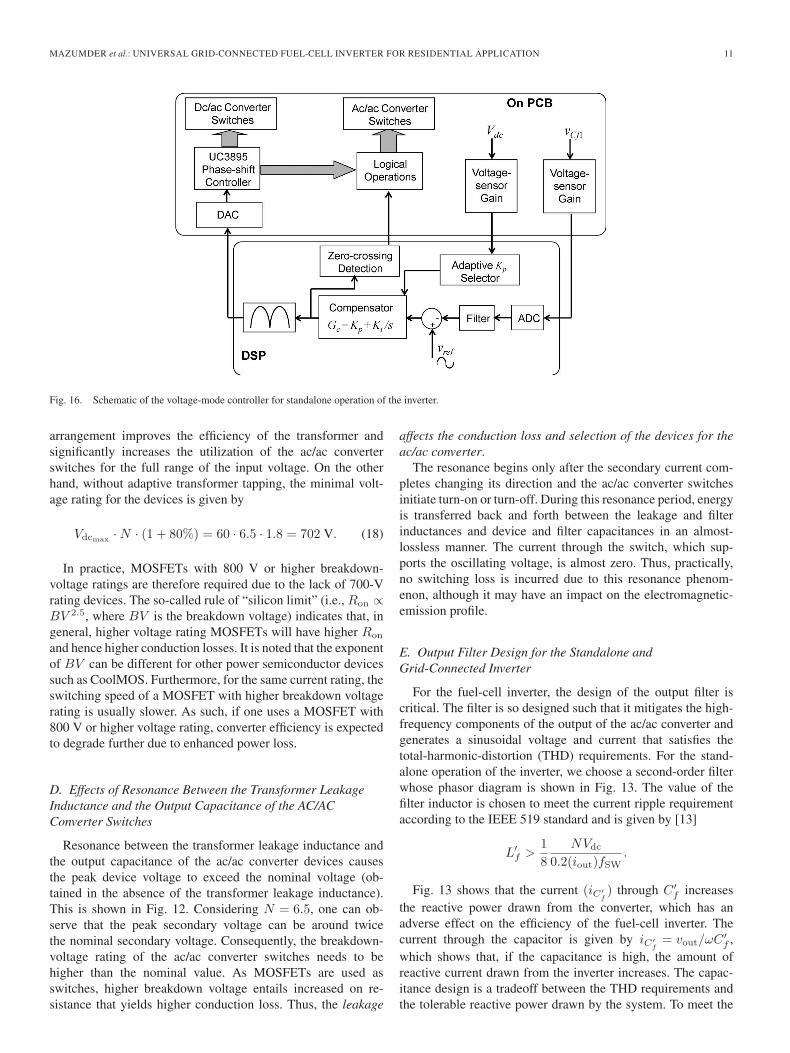
Fig. 14. Two filter designs (along with their respective phasor diagrams) forthe grid-connected inverter using (a) an L and (b) an LCL filter, connectedbetween the inverter and the grid. Symbols v′
ac/ac, L′
f , and C′f represent
the equivalent output voltage of the ac/ac converter and the equivalent filterinductance and capacitance for 120- and 240-V ac output operations. SymbolLf3 represents the inductance between the grid and the inverter.
Fig. 15. Schematics of the converters for (a) the standalone and (b) grid-connected modes of operation. An SPDT relay is used to switch between thetwo modes of operation.
MAZUMDER et al.: UNIVERSAL GRID-CONNECTED FUEL-CELL INVERTER FOR RESIDENTIAL APPLICATION 11
Fig. 16. Schematic of the voltage-mode controller for standalone operation of the inverter.
arrangement improves the efficiency of the transformer andsignificantly increases the utilization of the ac/ac converterswitches for the full range of the input voltage. On the otherhand, without adaptive transformer tapping, the minimal volt-age rating for the devices is given by
Vdcmax · N · (1 + 80%) = 60 · 6.5 · 1.8 = 702 V. (18)
In practice, MOSFETs with 800 V or higher breakdown-voltage ratings are therefore required due to the lack of 700-Vrating devices. The so-called rule of “silicon limit” (i.e., Ron ∝BV 2.5, where BV is the breakdown voltage) indicates that, ingeneral, higher voltage rating MOSFETs will have higher Ron
and hence higher conduction losses. It is noted that the exponentof BV can be different for other power semiconductor devicessuch as CoolMOS. Furthermore, for the same current rating, theswitching speed of a MOSFET with higher breakdown voltagerating is usually slower. As such, if one uses a MOSFET with800 V or higher voltage rating, converter efficiency is expectedto degrade further due to enhanced power loss.
D. Effects of Resonance Between the Transformer LeakageInductance and the Output Capacitance of the AC/ACConverter Switches
Resonance between the transformer leakage inductance andthe output capacitance of the ac/ac converter devices causesthe peak device voltage to exceed the nominal voltage (ob-tained in the absence of the transformer leakage inductance).This is shown in Fig. 12. Considering N = 6.5, one can ob-serve that the peak secondary voltage can be around twicethe nominal secondary voltage. Consequently, the breakdown-voltage rating of the ac/ac converter switches needs to behigher than the nominal value. As MOSFETs are used asswitches, higher breakdown voltage entails increased on re-sistance that yields higher conduction loss. Thus, the leakage
affects the conduction loss and selection of the devices for theac/ac converter.
The resonance begins only after the secondary current com-pletes changing its direction and the ac/ac converter switchesinitiate turn-on or turn-off. During this resonance period, energyis transferred back and forth between the leakage and filterinductances and device and filter capacitances in an almost-lossless manner. The current through the switch, which sup-ports the oscillating voltage, is almost zero. Thus, practically,no switching loss is incurred due to this resonance phenom-enon, although it may have an impact on the electromagnetic-emission profile.
E. Output Filter Design for the Standalone andGrid-Connected Inverter
For the fuel-cell inverter, the design of the output filter iscritical. The filter is so designed such that it mitigates the high-frequency components of the output of the ac/ac converter andgenerates a sinusoidal voltage and current that satisfies thetotal-harmonic-distortion (THD) requirements. For the stand-alone operation of the inverter, we choose a second-order filterwhose phasor diagram is shown in Fig. 13. The value of thefilter inductor is chosen to meet the current ripple requirementaccording to the IEEE 519 standard and is given by [13]
L′f >
18
NVdc
0.2(iout)fSW.
Fig. 13 shows that the current (iC′f) through C ′
f increasesthe reactive power drawn from the converter, which has anadverse effect on the efficiency of the fuel-cell inverter. Thecurrent through the capacitor is given by iC′
f= vout/ωC ′
f ,which shows that, if the capacitance is high, the amount ofreactive current drawn from the inverter increases. The capac-itance design is a tradeoff between the THD requirements andthe tolerable reactive power drawn by the system. To meet the

12 IEEE TRANSACTIONS ON INDUSTRIAL ELECTRONICS, VOL. 57, NO. 10, OCTOBER 2010
Fig. 17. (a) Schematic of the voltage-mode controller for the standalone inverter just before grid connection. (b) Schematic of the current-injection controller forthe inverter after it is connected to the grid.
requirements of the IEEE 519 standard, the value of the filtercapacitance is chosen to be [13]
C ′f = (%PReactive)
Poutrated
ωv2out
where %PReactive is the tolerable reactive power and Poutrated
is the rated output power of the inverter.For the grid-connected operation, the inverter should have
an inductive output to minimize the inrush current be-tween the grid and the inverter. In Fig. 14, we outline twopossible choices: a single-inductor (L) and an inductive–capacitive–inductive (LCL) filter. In [14] and [15], a simpleL filter is proposed for the grid connection. However, to meetthe regulatory standards of IEEE 519 or IEC 61000-3-2, the sizeof such an inductor has to be significantly large. This is mainlybecause the inductor has to bypass the higher order harmonicsof the ac/ac output. Hence, we choose an LCL filter, as shown
TABLE IISOME KEY DESIGN SPECIFICATIONS FOR THE INVERTER [1], [2]
MAZUMDER et al.: UNIVERSAL GRID-CONNECTED FUEL-CELL INVERTER FOR RESIDENTIAL APPLICATION 13
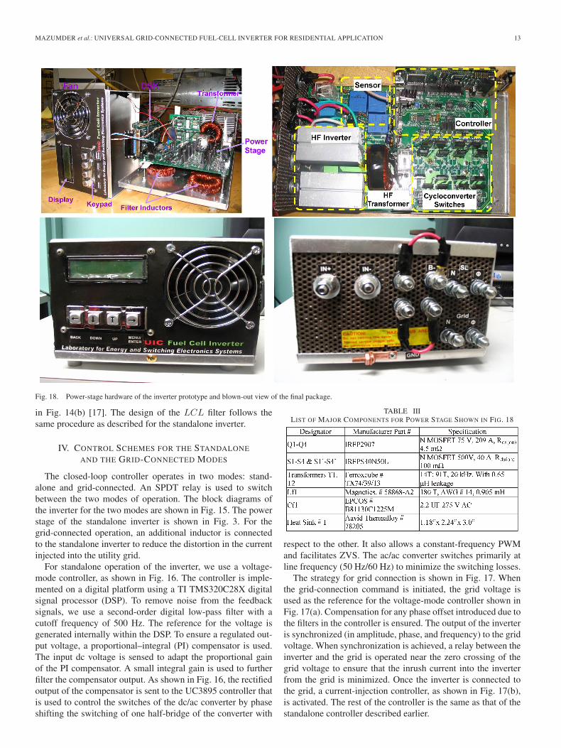
Fig. 18. Power-stage hardware of the inverter prototype and blown-out view of the final package.
in Fig. 14(b) [17]. The design of the LCL filter follows thesame procedure as described for the standalone inverter.
IV. CONTROL SCHEMES FOR THE STANDALONE
AND THE GRID-CONNECTED MODES
The closed-loop controller operates in two modes: stand-alone and grid-connected. An SPDT relay is used to switchbetween the two modes of operation. The block diagrams ofthe inverter for the two modes are shown in Fig. 15. The powerstage of the standalone inverter is shown in Fig. 3. For thegrid-connected operation, an additional inductor is connectedto the standalone inverter to reduce the distortion in the currentinjected into the utility grid.
For standalone operation of the inverter, we use a voltage-mode controller, as shown in Fig. 16. The controller is imple-mented on a digital platform using a TI TMS320C28X digitalsignal processor (DSP). To remove noise from the feedbacksignals, we use a second-order digital low-pass filter with acutoff frequency of 500 Hz. The reference for the voltage isgenerated internally within the DSP. To ensure a regulated out-put voltage, a proportional–integral (PI) compensator is used.The input dc voltage is sensed to adapt the proportional gainof the PI compensator. A small integral gain is used to furtherfilter the compensator output. As shown in Fig. 16, the rectifiedoutput of the compensator is sent to the UC3895 controller thatis used to control the switches of the dc/ac converter by phaseshifting the switching of one half-bridge of the converter with
TABLE IIILIST OF MAJOR COMPONENTS FOR POWER STAGE SHOWN IN FIG. 18
respect to the other. It also allows a constant-frequency PWMand facilitates ZVS. The ac/ac converter switches primarily atline frequency (50 Hz/60 Hz) to minimize the switching losses.
The strategy for grid connection is shown in Fig. 17. Whenthe grid-connection command is initiated, the grid voltage isused as the reference for the voltage-mode controller shown inFig. 17(a). Compensation for any phase offset introduced due tothe filters in the controller is ensured. The output of the inverteris synchronized (in amplitude, phase, and frequency) to the gridvoltage. When synchronization is achieved, a relay between theinverter and the grid is operated near the zero crossing of thegrid voltage to ensure that the inrush current into the inverterfrom the grid is minimized. Once the inverter is connected tothe grid, a current-injection controller, as shown in Fig. 17(b),is activated. The rest of the controller is the same as that of thestandalone controller described earlier.
14 IEEE TRANSACTIONS ON INDUSTRIAL ELECTRONICS, VOL. 57, NO. 10, OCTOBER 2010
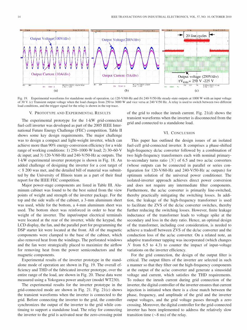
Fig. 19. Experimental waveforms for standalone mode of operation. (a) 120-V/60-Hz and (b) 240-V/50-Hz steady-state outputs at 1000 W with an input voltageof 30 V. (c) Transient output voltage when the load changes from 250 to 3000 W and vice versa at 240 V/50 Hz. A relay is used to switch between two differentload conditions, and the trigger signal for the relay is shown in the top trace.
V. PROTOTYPE AND EXPERIMENTAL RESULTS
The experimental prototype for the 1-kW grid-connectedfuel-cell inverter was developed as part of the 2005 IEEE Inter-national Future Energy Challenge (FEC) competition. Table IIshows some key design requirements. The major challengewas to design a compact and light-weight inverter, which canachieve more than 90% energy-conversion efficiency for a widerange of working conditions: 1) 250–1000-W load; 2) 30–60-Vdc input; and 3) 120-V/60-Hz and 240-V/50-Hz ac outputs. The1-kW experimental inverter prototype is shown in Fig. 18. Anadded challenge of designing the inverter for a cost target of< $ 200 was met, and the detailed bill of material was submit-ted by the University of Illinois team as a part of their finalreport for the IEEE FEC competition.
Major power-stage components are listed in Table III. Alu-minum cabinet was found to be the best suited from the viewpoints of weight and strength of the inverter package. For thetop and the side walls of the cabinet, a 3-mm aluminum sheetwas used, while for the bottom, a 4-mm aluminum sheet wasused. The bottom sheet was reinforced in order to bear theweight of the inverter. The input/output electrical terminalswere located at the rear of the inverter, while the keypad, theLCD display, the fan, and the parallel port for programming theDSP starter kit were located at the front. All of the magneticcomponents were clamped to the base of the cabinet, whichalso removed heat from the windings. The perforated windowsand the fan were strategically placed to maximize the airflowfor removing heat from the power semiconductors and themagnetic components.
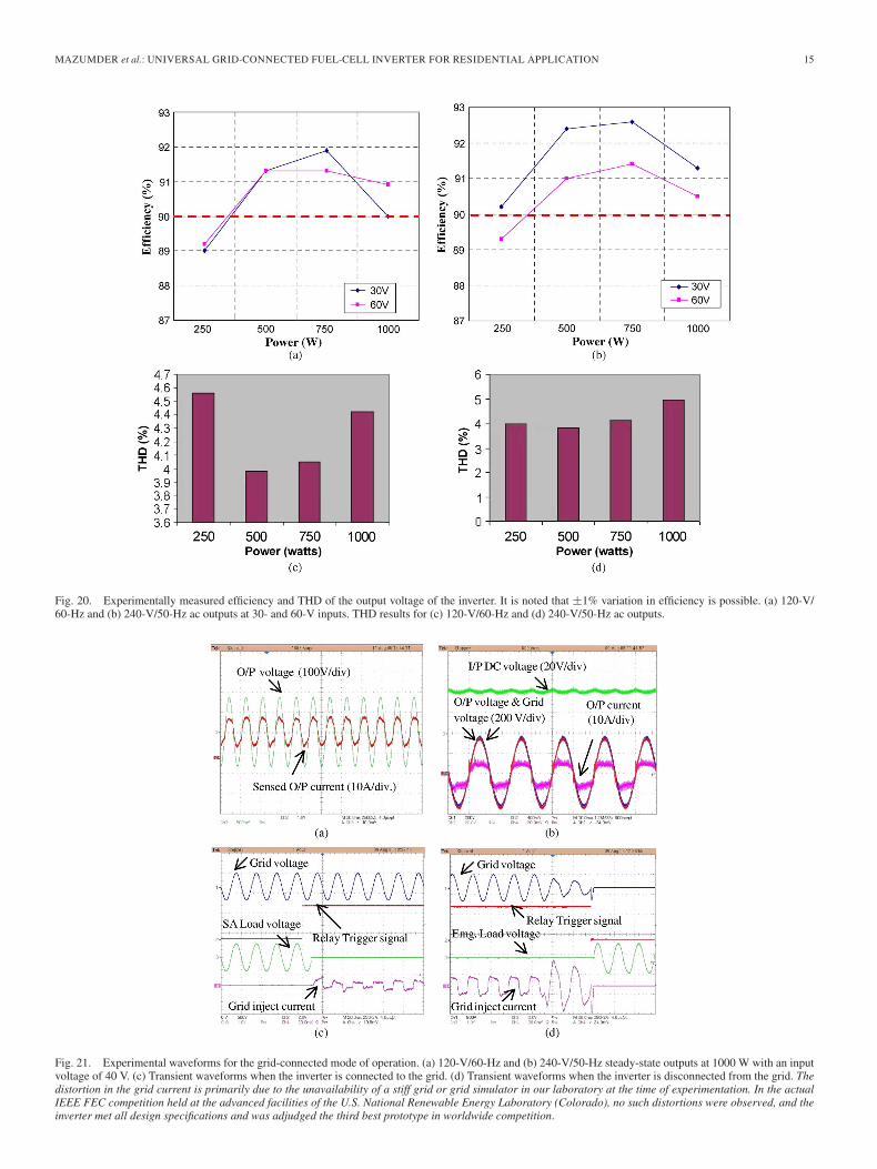
Experimental results of the inverter prototype in the stand-alone mode of operation are shown in Fig. 19. The overall ef-ficiency and THD of the fabricated inverter prototype, over theentire range of the load, are shown in Fig. 20. These data weremeasured using a Yokogawa power analyzer (model WT230).
The experimental results for the inverter prototype in thegrid-connected mode are shown in Fig. 21. Fig. 21(c) showsthe transient waveforms when the inverter is connected to thegrid. Before connecting the inverter to the grid, the controllersynchronizes the output of the inverter to the grid while con-tinuing to support a standalone load. The relay for connectingthe inverter to the grid is activated near the zero-crossing point
of the grid to reduce the inrush current. Fig. 21(d) shows thetransient waveforms when the inverter is disconnected from thegrid and connected to a standalone load.
VI. CONCLUSION
This paper has outlined the design issues of an isolatedfuel-cell grid-connected inverter. It comprises a phase-shiftedhigh-frequency dc/ac converter followed by a combination oftwo high-frequency transformers each with nominal primary-to-secondary turns ratio (N) of 6.5 and two ac/ac converters(whose outputs can be connected in parallel or series con-figuration for 120-V/60-Hz and 240-V/50-Hz ac outputs) foroptimum solution of the universal power conditioner. Theisolated-inverter approach achieves direct power conversionand does not require any intermediate filter components.Furthermore, the ac/ac converter is primarily line-switched,thereby practically mitigating the switching losses. In addi-tion, the leakage of the high-frequency transformer is usedto facilitate the ZVS of the dc/ac converter switches, therebyfurther reducing the switching losses. However, finite leakageinductance of the transformer leads to voltage spike at thesecondary and loss in the duty ratio. Hence, an optimal designof the transformer, including cost consideration, is needed toachieve a tradeoff between ZVS of the dc/ac converter and theconduction loss of the ac/ac converter. On a related note, anadaptive transformer tapping was incorporated (which changesN from 6.5 to 4.3) to counter the impact of input-voltagevariations on the inverter efficiency.
For the grid connection, the design of the output filter iscritical. The output filters of the inverter are selected in sucha manner so that they filter out the high-frequency componentsat the output of the ac/ac converter and generate a sinusoidalvoltage and current, which satisfies the THD requirements.To reduce the inrush current during grid connection of theinverter, the digital controller of the inverter ensures that currentinjection is initiated when there is a close match between thephase, frequency, and amplitude of the grid and the inverteroutput voltages, and the grid voltage passes through a zerocrossing. Moreover, the digital controller for the grid-connectedinverter has been implemented to address the relatively slowtransition time (∼8 ms) of the relay.
MAZUMDER et al.: UNIVERSAL GRID-CONNECTED FUEL-CELL INVERTER FOR RESIDENTIAL APPLICATION 15
Fig. 20. Experimentally measured efficiency and THD of the output voltage of the inverter. It is noted that ±1% variation in efficiency is possible. (a) 120-V/60-Hz and (b) 240-V/50-Hz ac outputs at 30- and 60-V inputs. THD results for (c) 120-V/60-Hz and (d) 240-V/50-Hz ac outputs.
Fig. 21. Experimental waveforms for the grid-connected mode of operation. (a) 120-V/60-Hz and (b) 240-V/50-Hz steady-state outputs at 1000 W with an inputvoltage of 40 V. (c) Transient waveforms when the inverter is connected to the grid. (d) Transient waveforms when the inverter is disconnected from the grid. Thedistortion in the grid current is primarily due to the unavailability of a stiff grid or grid simulator in our laboratory at the time of experimentation. In the actualIEEE FEC competition held at the advanced facilities of the U.S. National Renewable Energy Laboratory (Colorado), no such distortions were observed, and theinverter met all design specifications and was adjudged the third best prototype in worldwide competition.

16 IEEE TRANSACTIONS ON INDUSTRIAL ELECTRONICS, VOL. 57, NO. 10, OCTOBER 2010
Methodologies for further improvements in the overallenergy-conversion efficiency of the inverter while simultane-ously operating at higher switching frequency (for enhancedpower density), using advanced semiconductor switches andsoft-switching techniques, are being investigated. Extendingthe operation of the single-phase inverter for photovoltaicand battery-based sources as well as for higher power mul-tiphase operation has added foci of our current research anddevelopment.
ACKNOWLEDGMENT
Any opinions, findings, conclusions, or recommendationsexpressed herein are those of the authors and do not necessarilyreflect the views of the National Science Foundation or the U.S.Department of Energy.
REFERENCES
[1] S. K. Mazumder, R. K. Burra, R. Huang, M. Tahir, K. Acharya, G. Garcia,S. Pro, O. Rodrigues, and M. Stasinopoulos, “Single-stage low-cost andenergy-efficient isolated phase-shifted high-frequency inverter followedby a forced cycloconverter for universal residential fuel cell power sys-tem,” in Proc. IEEE Electro/Inf. Technol. Conf., Ames, IA, May 2008,pp. 408–413.
[2] S. Jung, Y. Bae, S. Choi, and H. Kim, “A low cost utility interactiveinverter for residential fuel cell generation,” IEEE Trans. Power Electron.,vol. 22, no. 6, pp. 2293–2298, Nov. 2007.
[3] B. S. Prasad, S. Jain, and V. Agarwal, “Universal single-stage grid-connected inverter,” IEEE Trans. Energy Convers., vol. 23, no. 1, pp. 128–137, Mar. 2008.
[4] H. Tao, J. L. Duarte, and M. A. M. Hendrix, “Line-interactive UPS using afuel cell as the primary source,” IEEE Trans. Ind. Electron., vol. 55, no. 8,pp. 3012–3021, Aug. 2008.
[5] G. K. Andersen, C. Klumpner, S. B. Kjaer, and F. Blaabjerg, “A new greenpower inverter for fuel cells,” in Proc. IEEE Power Electron. Spec. Conf.,2002, vol. 2, pp. 727–733.
[6] R. Gopinath, S. Kim, J. Han, P. N. Enjeti, M. B. Yeary, and J. W. Howze,“Development of a low cost fuel cell inverter system with DSP control,”IEEE Trans. Power Electron., vol. 19, no. 5, pp. 1256–1262, Sep. 2004.
[7] S. K. Mazumder, R. K. Burra, and K. Acharya, “A ripple-mitigating andenergy-efficient fuel cell power-conditioning system,” IEEE Trans. PowerElectron., vol. 22, no. 4, pp. 1437–1452, Jul. 2007.
[8] S. Deng, H. Mao, J. Mazumdar, I. Batarseh, and K. K. J. Islam, “A newcontrol scheme for high-frequency link inverter design,” in Proc. IEEEAppl. Power Electron. Conf., 2003, pp. 512–517.
[9] T. Kawabata, H. Komji, K. Sashida, K. Sanada, and M. Koyama, “Highfrequency link dc/ac converter with PWM cycloconverter,” in Conf. Rec.IEEE IAS Annu. Meeting, 1990, pp. 1119–1124.
[10] M. Matsui, M. Nagai, M. Mochizuki, and A. Nabae, “A high-frequencylink dc/ac converter with suppressed voltage clamp circuits-naturally com-mutated phase angle control with self turn-off devices,” IEEE Trans. Ind.Appl., vol. 32, no. 2, pp. 293–300, Mar./Apr. 1996.
[11] J. A. Sabate and V. Vlatkovic, “Design considerations for high-voltagehigh-power full-bridge zero-voltage-switched PWM converter,” in Conf.Rec. IEEE IAS Annu. Meeting, 1990, pp. 275–284.
[12] K. Wang, F. C. Lee, and W. Dong, “New soft-switched quasi-single-stage (QSS) bi-directional inverter/charger,” in Conf. Rec. IEEE IAS Annu.Meeting, 1999, pp. 2031–2038.
[13] T. C. Y. Wang, Z. Ye, G. Sinha, and X. Yuan, “Output filter design for agrid-interconnected three phase inverter,” in Proc. IEEE Power Electron.Spec. Conf., 2003, pp. 779–784.
[14] M. Ashari, C. V. Nayar, and S. Islam, “Steady-state performance of agrid interactive voltage source inverter,” in Proc. IEEE Power Eng. Soc.Summer Meeting, 2001, vol. 1, pp. 650–655.
[15] Q. Chongming and K. M. Smedley, “Three-phase grid-connected in-verters interface for alternative energy sources with unified constant-frequency integration control,” in Conf. Rec. IEEE IAS Annu. Meeting,2001, pp. 2675–2682.
[16] S. Daher, J. Schmid, and F. L. M. Antunes, “Multilevel inverter topologiesfor standalone PV systems,” IEEE Trans. Ind. Electron., vol. 55, no. 7,pp. 2703–2712, Jul. 2008.
[17] M. Liserre, R. Teodorescu, and F. Blaabjerg, “Stability of grid-connectedPV inverters with large grid impedance variation,” in Proc. IEEE PowerElectron. Spec. Conf., 2004, pp. 4773–4779.
[18] R. Huang and S. K. Mazumder, “A novel soft-switching scheme for anisolated dc/dc converter with pulsating dc output for a three-phase high-frequency-link PWM converter,” in Conf. Rec. IEEE IAS Annu. Meeting,2008, pp. 1–9.
[19] S. K. Mazumder, “A novel hybrid modulation scheme for an isolated high-frequency-link fuel cell inverter,” presented at the IEEE Power Engineer-ing Society Conf., Pittsburgh, PA, Jul., 2008, Invited National ScienceFoundation Panel Paper. [Online]. Available: Paper PESGM2006-000737
[20] S. K. Mazumder, R. K. Burra, R. Huang, and V. Arguelles, “A low-cost single-stage isolated differential Cuk inverter for fuel cell applica-tion,” in Proc. IEEE Power Electron. Spec. Conf., Rhodes, Greece, 2008,pp. 4426–4430.
[21] S. K. Mazumder, T. Sarkar, and K. Acharya, “A directFET based high-frequency fuel-cell inverter,” in Proc. IEEE Appl. Power Electron. Conf.,2009, pp. 1805–1812.
Sudip K. Mazumder (SM’03) received the M.S.degree in electrical power engineering from Rensse-laer Polytechnic Institute, Troy, NY, in 1993 and thePh.D. degree in electrical and computer engineeringfrom Virginia Polytechnic Institute and State Univer-sity, Blacksburg, in 2001.
He is currently the Director of the Laboratoryfor Energy and Switching Electronics Systems, De-partment of Electrical and Computer Engineering,University of Illinois at Chicago, Chicago, where heis also an Associate Professor. He is a Reviewer for
multiple international journals and conferences. He was the Editor-in-Chief forthe International Journal of Power Management Electronics between 2006 and2009. He has over 15 years of professional experience and has held R&Dand design positions in leading industrial organizations. He has publishedover 100 refereed and invited journals and conference papers. His currentareas of interests are interactive power electronics/power networks, renewableand alternate energy systems, photonically triggered and wide-bandgap powersemiconductor devices, and applied technologies.
Dr. Mazumder has been serving as an Associate Editor for the IEEETRANSACTIONS ON INDUSTRIAL ELECTRONICS since 2003 and for the IEEETRANSACTIONS ON AEROSPACE AND ELECTRONIC SYSTEMS since 2008.He was an Associate Editor for the IEEE POWER ELECTRONICS LETTERS
until 2005. He is the Chair of the Student/Industry Coordination Activities forthe IEEE Energy Conversion Congress and Exposition for 2009 and 2010.Since 2009, he has been the Cochair for the IEEE PELS Committee onSustainable Energy Systems and the Vice Chair for the Technical Subcommitteeon Distributed Generation and Renewable Energy. He has been invited bythe IEEE and the American Society of Mechanical Engineers as well asmultiple industries, federal agencies, national laboratories, and universities forseveral keynote, plenary, and invited lectures and presentations. He was therecipient of the prestigious 2008 and 2006 Faculty Research Awards from theUniversity of Illinois for excellent scholarly work and outstanding researchperformance. He was also the recipient of the National Science FoundationCAREER Award and the Office of Naval Research Young Investigator Awardin 2003 and 2005, respectively, and the recipient of the Prize Paper Award fromthe IEEE TRANSACTIONS ON POWER ELECTRONICS and the IEEE PowerElectronics Society (PELS) in 2002. He was also the corecipient of the 2007IEEE Outstanding Student Paper Award at the IEEE International Conferenceon Advanced Information Networking and Applications with Dr. M. Tahir. Hewas also a recipient of the 2005 IEEE Future Energy Challenge Energy Award.
Rajni K. Burra (M’10) received the B.Tech. degreein electronics and communication engineering fromthe Indian Institute of Technology, Kharagpur, India,in 2000 and the M.S. and Ph.D. degrees in elec-trical engineering from the University of Illinois atChicago, Chicago, in 2003 and 2006, respectively.
He is currently a Research Engineer with theGE Global Research Center, Bangalore, India. Hehas published over 13 refereed international journalsand conference papers. His research interests includenonconventional and renewable energy systems, ac-
tive power filtering, and power semiconductor devices.

MAZUMDER et al.: UNIVERSAL GRID-CONNECTED FUEL-CELL INVERTER FOR RESIDENTIAL APPLICATION 17
Rongjun Huang received the B.Eng. and M.Eng.degrees in electrical engineering from JiaotongUniversity, Beijing, China, in 1998 and 2001, respec-tively, and the Ph.D. degree from the Department ofElectrical and Computer Engineering, University ofIllinois at Chicago, Chicago, in 2009.
In 2001, he was an R&D Engineer with HuaweiTechnologies, Shenzhen, China. Currently, he is withInternational Rectifier, San Jose, CA. He has pub-lished over ten refereed international journals andconference papers. His research interests include
power electronics for renewable energy sources, wide-bandgap power semi-conductors, and energy harvesting.
Dr. Huang serves as a Reviewer for the IEEE TRANSACTIONS OF INDUS-TRIAL ELECTRONICS, IEEE TRANSACTIONS ON AEROSPACE AND ELEC-TRONIC SYSTEMS, and several international conferences.
Muhammad Tahir (M’09) received the Ph.D. de-gree in electrical and computer engineering from theUniversity of Illinois at Chicago, Chicago.
Before joining the University of Illinois for hisPh.D., he was a Lecturer with the Department ofElectrical Engineering, University of Engineeringand Technology, Lahore, Pakistan. Between 2008and 2009, he was a Postdoctoral Research Fellowwith the Institute of Microelectronics and WirelessSystems, National University of Ireland, Maynooth,Ireland. Currently, he is an Assistant Professor with
the University of Engineering and Technology. His current research focuseson the area of sensor integration and wireless multimedia sensor networks.His research interests include delay-constrained wireless networks, distributedcommunication network resource optimization, and real-time wireless multi-media networks.
Dr. Tahir was the corecipient of the Outstanding Student Paper Award at the21st IEEE International Conference on Advanced Information Networking andApplications.
Kaustuva Acharya (M’09) received the B.Eng. de-gree in electronics and communication engineeringfrom the Regional Engineering College (now theNational Institute of Technology), Bhopal, India, in2000 and the M.S. and Ph.D. degrees in electrical en-gineering from the University of Illinois at Chicago,Chicago, in 2003 and 2008, respectively.
Between 2003 and 2008, he was a Research Assis-tant with the Laboratory for Energy and Switching-Electronics Systems, University of Illinois atChicago. Subsequently, he was a Postdoctoral Re-
search Associate with the same laboratory between 2008 and 2009 beforeaccepting a position at Texas Instruments. He has published over 20 refereed in-ternational journals and conference papers. His research interests include powerelectronics for renewable and alternate energy sources, and modeling, analyses,and control of interactive power networks for distributed power systems.
Dr. Acharya is a Reviewer for the IEEE TRANSACTIONS ON POWER
ELECTRONICS, IEEE TRANSACTIONS ON INDUSTRIAL ELECTRONICS, andseveral international conferences. He copresented a tutorial entitled “Globalstability methodologies for switching power converters” at the IEEE PowerElectronics Specialists Conference, 2007.
IEEE TRANSACTIONS ON INDUSTRIAL ELECTRONICS, VOL. 57, NO. 10, OCTOBER 2010 1
A Universal Grid-Connected Fuel-Cell Inverter forResidential Application
Sudip K. Mazumder, Senior Member, IEEE, Rajni K. Burra, Member, IEEE, Rongjun Huang,Muhammad Tahir, Member, IEEE, and Kaustuva Acharya, Member, IEEE
Abstract—This paper describes a universal fuel-cell-based grid-connected inverter design with digital-signal-processor-based digi-tal control. The inverter has a direct power conversion mechanismwith a high-frequency zero-voltage-switched dc/ac primary-sideconverter followed by a pair of ac/ac cycloconverters that operateseither in parallel or in series to simultaneously address the issuesof universal output and high efficiency. The critical design issuesfocus on the impact and optimization of transformer leakageinductance with regard to effectiveness of zero voltage switchingof a primary-side converter, duty-cycle loss, resonance, and voltagespike that has effect on the breakdown voltage rating of the cyclo-converter devices. An additional concept of dynamic transformertapping has been explored to address the impact of varying inputvoltage on secondary-side voltage spike and inverter efficiency.Finally, detailed grid-parallel and grid-connected results are pre-sented that demonstrate satisfactory inverter performances.
Index Terms—AC/AC, control, dc/ac, digital signal processor(DSP), fuel cell, grid, high frequency, inverter, residential.
I. INTRODUCTION
THE utilization of fuel cells for distributed power gen-eration requires the development of a low-cost, high-
efficiency, and universal power-electronic system that convertsa fuel cell’s low-voltage output, which usually varies from 30 to60 V for residential application, into commercial 120-V/60-Hzand 240-V/50-Hz ac outputs [1]–[3]. In addition, the power-electronic system should have the following characteristics:1) output-voltage regulation for a wide variation in the outputvoltage of the fuel-cell stack; 2) capability for standaloneand grid-connected operations; 3) low output harmonics; and4) high energy-conversion efficiency.
Manuscript received August 25, 2008; revised December 30, 2008; acceptedMarch 4, 2009. This work was supported in part by the U.S. National ScienceFoundation under Awards 0725887 and 0239131 and in part by the U.S. Depart-ment of Energy under Award DE-FC2602NT41574. However, any opinions,findings, conclusions, or recommendations expressed herein are those of theauthors and do not necessarily reflect the views of the U.S. National ScienceFoundation or the U.S. Department of Energy.
S. K. Mazumder is with the Laboratory for Energy and Switching ElectronicsSystems, Department of Electrical and Computer Engineering, University ofIllinois at Chicago, Chicago, IL 60607 USA (e-mail: [email protected]).
R. K. Burra is with the GE Global Research Center, Bangalore 560 066, India(e-mail: [email protected]).
R. Huang is with International Rectifier, San Jose, CA 95134-1902 USA(e-mail: [email protected]).
M. Tahir is with the University of Engineering and Technology, Lahore54890, Pakistan (e-mail: [email protected]).
K. Acharya is with Texas Instruments Incorporated, Dallas, TX 75243 USA.Color versions of one or more of the figures in this paper are available online
at http://ieeexplore.ieee.org.Digital Object Identifier 10.1109/TIE.2009.2038943
Fig. 1. Power-conditioning scheme with (a) line-frequency transformer,(b) high-frequency transformer in the dc/ac stage [7], (c) high-frequencytransformer in the dc/dc stage [18], [19], and (d) single-stage isolated dc/acconverter [20].
Fig. 1(a)–(c) shows three mechanisms for achieving galvanicisolation between the fuel-cell stack and the application load.The conventional scheme, shown in Fig. 1(a), achieves isolationby placing a 50-Hz/60-Hz line-frequency transformer at theoutput of the inverter. Such a transformer is bulky because it hasto handle low-frequency currents and voltages. The other twooptions, shown in Fig. 1(b) and (c), achieve isolation by placingthe transformer within the power-conditioning system. Thehigh-frequency isolation can be included in the dc/ac converterstage, as shown in Fig. 1(b) [7], or in the dc/dc converterstage, as shown in Fig. 1(c) [18], [19]. Fig. 1(d) shows aneven more compact power-electronics option [20]. The single-stage isolated topology requires either a higher fuel-cell-stack
0278-0046/$26.00 © 2010 IEEE

2 IEEE TRANSACTIONS ON INDUSTRIAL ELECTRONICS, VOL. 57, NO. 10, OCTOBER 2010
Fig. 2. Block diagram of high-frequency link inverter configurations:(a) dc/dc-type and (b) cycloconverter-type converter configurations.
voltage or slightly higher turns ratio of the transformer fora lower stack voltage to generate the needed 120-V/240-Vline output. Overall, the isolation transformers for the schemesshown in Fig. 1(b)–(d) operate at high frequency and, hence, aresignificantly smaller than the line-frequency transformer shownin Fig. 1(a).
With regard to an isolated inverter, several topological con-figurations have been proposed to achieve fuel-cell power con-version at high efficiency without incurring high cost [1]–[10].Based on where the transformer is inserted for isolating thestack from the load, these topologies can be broadly classifiedinto two categories. The first one is referred to as the “dc/dc-type converter” and is shown in Fig. 2(a). It comprises ahigh-frequency dc/ac converter followed by a high-frequencytransformer, a diode rectifier (inserted at the secondary of thetransformer), and a link filter to obtain a higher dc voltage.Following this isolated dc/dc stage, a dc/ac converter is insertedto obtain a low-frequency ac. Because this type of topology hasthree power-conversion stages, it may not always be a suitablechoice from efficiency and cost point of views because each ofthe power stages has to have very high efficiency. Furthermore,with increasing output power, the size and the cost of the dc-link filter attain significance.
The second topology, outlined in this paper and referred to asthe “cycloconverter-type converter,” is shown in Fig. 2(b). Thisarchitecture supports bidirectional power flow and reduces sys-tem complexity by removing the rectifier and the dc-link filter.Galvanic isolation is achieved by embedding the transformerinto the overall inverter, which usually comprises a two-level orhigher level dc/ac converter followed by an ac/ac converter [1],[7], [8], [16].
Fig. 3 shows a circuit diagram of the proposed universalinverter with input voltage varying between 30 and 60 V. Itcomprises a phase-shifted full-bridge dc/ac converter as a com-mon primary stage followed by two identical high-frequencystep-up transformers and two forced ac/ac converters. SwitchesQ1−Q4 of the dc/ac converter are sinusoidally modulated tocreate a high-frequency ac voltage, which is converted into a60-Hz/50-Hz line-frequency ac by a combination of the ac/ac
converters and the LC output filters. As shown in Fig. 3(a) and(b), for 120- and 240-V ac outputs, the two filter capacitorsof the ac/ac converters are connected in parallel and in series,respectively.
Phase-shifted control of the dc/ac converter enables Q1−Q4
to be turned on under a zero-voltage-switching (ZVS) condi-tion due to the resonance between the primary-side leakageinductance of the high-frequency transformer and the output ca-pacitances of the MOSFETs [11]. Unlike the complex schemesoutlined in the literature [9], [10], [12], which implement high-frequency switching for both the dc/ac converter and the ac/acconverter stages, the ac/ac converter switches in the controlscheme outlined in this paper (see Figs. 16 and 17) are commu-tated primarily at line frequency when the polarities of outputcurrent and output voltage are the same and at high frequencywhen the polarities are opposite. Thus, under unity-power-factor operation, due to line-frequency switching, the ac/acconverter switching losses are significantly reduced.
Furthermore, unlike the topology outlined in [9] and [10], foran uninterruptible-power-supply application that usually has ahigh input voltage, in a fuel-cell-inverter application, owing tothe low stack voltage, a step-up transformer with high turnsratio is necessary to obtain the rated ac output. For instance,for an input of 30 V, the primary-to-secondary turns ratio (N)of the transformer is calculated to be 13 to achieve the desired240-V ac output. Fabrication of a 1-kW 1:13 high-frequencytransformer is relatively difficult. Furthermore, high turns ratioyields enhanced secondary leakage inductance and secondarywinding resistance, both of which result in a measurable lossin duty cycle and an increase in secondary copper loss. Higherleakage inductance also leads to higher voltage spike, whichadds to the high nominal voltage of the secondary and ne-cessitates the use of high-voltage power devices for the ac/acconverter. Such devices usually have higher on resistance andslower switching speeds, both of which diminish the overallsystem efficiency.
This paper addresses key design issues related to these chal-lenges and proposes simple but effective solutions to improveefficiency. The focus of the design issues is on the effects oftransformer leakage inductance on the ZVS and loss in the dutycycle of the dc/ac converter and on resonance, which results involtage spike that affects the breakdown-voltage rating of theac/ac converter devices. The concept of dynamic transformertapping has been investigated to address the effects of input-voltage variation on voltage-spike mitigation and inverter effi-ciency. Subsequently, the control strategies for standalone andgrid-connected operations and experimental design of a 1-kWinverter prototype are described. The experimental results andperformances verify the effectiveness of the inverter and showits promising applications for fuel-cell as well as photovoltaicand battery-based power systems.
II. PRINCIPLES OF OPERATION
The basic schematic of the proposed universal inverter isshown in Fig. 4(a) and is used in the following sections tosimplify the analysis. The ac/ac converters are switched basedon output-voltage polarity, since primarily, unity-power-factor
MAZUMDER et al.: UNIVERSAL GRID-CONNECTED FUEL-CELL INVERTER FOR RESIDENTIAL APPLICATION 3
Fig. 3. Circuit diagrams of the proposed fuel-cell inverter for (a) 120-V/60-Hz ac and (b) 240-V/50-Hz ac outputs. An SPDT switch enables adaptive tapping ofthe transformer.
operation is required for the present design, and hence, theduration for which the polarities of the output voltage andcurrent are different is negligibly small. The circuit schematicis the same as a conventional transformer-isolated full-bridgepulsewidth-modulation (PWM)-based dc/dc converter but hastwo different sets of rectifier arrangements for the positiveand negative line cycles, as shown in Fig. 4(b) and (c). Anillustration of the inverter operation is shown in Fig. 4(d),taking into account the two secondary-side ac/ac converters.Basically, the primary-side dc/ac converter is modulated tocreate a bipolar high-frequency waveform, which is amplified
by the transformer and eventually shaped by the secondary-sideac/ac converters to generate the desired output ac waveformafter passing the sinewave-modulated high-frequency signalsthrough the output LC filter. Because the dc/ac convertercreates the sinewave-modulated output, the ac/ac converterswitches do not need to force switch; they can simply operateat line frequency to rectify the bipolar sinewave-modulatedoutput. In practice, to preclude the reverse-recovery problemof the MOSFET, antiparallel diode, use of Schottky diode [21]or channel conduction of one of the MOSFETs [as shown inFig. 4(d)] may need to be adopted.

4 IEEE TRANSACTIONS ON INDUSTRIAL ELECTRONICS, VOL. 57, NO. 10, OCTOBER 2010
Fig. 4. (a) Circuit elements of the inverter. Power-stage circuits for (b) positive and (c) negative line cycles. (d) Gate-drive signals and key waveforms.
Next, we discuss the modes of operation for 120-V acoutput for an input-voltage range of 42–60 V (corresponding toN = 4.3). The modes of operation below 42 V (correspondingto N = 6.5) remain the same. The rationale for a tapped trans-former is provided in Section III-C. Fig. 5(f) shows the wave-forms for the five operating modes of the dc/ac converter forpositive primary and positive filter-inductor currents. Modes 2and 4 show the ZVS turn-on mechanism for switches Q4
and Q3, respectively. Overall, the five modes of the inverteroperation are discussed next for a positive primary current. Aset of five modes exists for a negative primary current as well. Asimilar set of five modes of operation and corresponding circuitconfigurations for 240-V ac output is shown in Fig. 6 for inputvoltage above 42 V (corresponding to N = 4.3). Again, themode of operation for input voltage below 42 V (correspondingto N = 6.5) remains the same.
Mode 1 [Fig. 5(a)]: During this mode, switches Q1 and Q2 ofthe dc/ac converter are on, and the transformer primary cur-rents ipri1 and ipri2 are positive. The output current (iout)splits equally between the two ac/ac converter modules.For the top ac/ac converter module, iout/2 is positive andflows through the switches S1 and S ′
1, the output filter Lf1
and Cf1, switches S2 and S ′2, and the transformer sec-
ondary. Similarly, for the bottom ac/ac converter module,iout/2 is positive and flows through the switches S5 andS ′
5, the output filter Lf2 and Cf2, switches S6 and S ′6, and
the transformer secondary.Mode 2 [Fig. 5(b)]: At the beginning of this interval, the gate
voltage of Q1 undergoes a high-to-low transition. As aresult, the output capacitance of Q1 begins to accumulatecharge, while the output capacitance of Q4 begins to dis-charge. Once the voltage across Q4 goes to zero, it can
MAZUMDER et al.: UNIVERSAL GRID-CONNECTED FUEL-CELL INVERTER FOR RESIDENTIAL APPLICATION 5
Fig. 5. Modes of operation for 120-V/60-Hz ac output for an input-voltage range of 42–60 V (corresponding to N = 4.3). (a)–(e) Topologies corresponding tothe five operating modes of the inverter for positive primary and positive filter-inductor currents. (f) Schematic waveforms show the operating modes of the dc/acconverter when primary currents are positive. The modes of operation below 42 V (corresponding to N = 6.5) remain the same.
6 IEEE TRANSACTIONS ON INDUSTRIAL ELECTRONICS, VOL. 57, NO. 10, OCTOBER 2010
Fig. 6. Modes of operation for 240-V/50-Hz ac output for an input-voltage range of 42–60 V (corresponding to N = 4.3). (a)–(e) Topologies corresponding tothe five operating modes of the inverter for positive primary and positive filter-inductor currents. (f) Schematic waveforms show the operating modes of the dc/acconverter when primary currents are positive. The modes of operation below 42 V (corresponding to N = 6.5) remain the same.
MAZUMDER et al.: UNIVERSAL GRID-CONNECTED FUEL-CELL INVERTER FOR RESIDENTIAL APPLICATION 7
be turned on under ZVS. The transformer primary currentsipri1 and ipri2 and the load current iout continue to flow inthe same direction.
Mode 3 [Fig. 5(c)]: This mode initiates when Q1 turns off.The transformer primary currents ipri1 and ipri2 are stillpositive and freewheel through Q4 as shown in Fig. 5(c).Moreover, the load current continues to flow in the samedirection as in Mode 2. Mode 3 ends when Q2 starts toturn off.
Mode 4 [Fig. 5(d)]: At the beginning of this interval, the gatevoltage of Q2 undergoes a high-to-low transition. As aresult, the output capacitance of Q2 begins to accumulatecharge, while the output capacitance of switch Q3 beginsto discharge, as shown in Fig. 5(d). The charging currentof Q2 and the discharging current of Q3 together add upto the primary currents ipri1 and ipri2. The transformer pri-mary currents make a transition from positive to negative.Once the voltage across Q3 goes to zero, it is turned onunder ZVS condition. The load current flows in the samedirection as in Mode 3 but makes a rapid transition fromthe bidirectional switches S1 and S ′
1 and S2 and S ′2 to S3
and S ′3 and S4 and S ′
4. During this process, iout/2 splitsbetween the two legs each of the ac/ac converter modulesas shown in Fig. 5(d). Mode 4 ends when the switch Q2 iscompletely turned off and its output capacitance is chargedto Vdc. At this point, it is necessary to note that, because S1
and S2 and S5 and S6 are off simultaneously, each of themsupports a voltage of Vdc.
Mode 5 [Fig. 5(e)]: This mode starts when Q2 is completelyturned off. The primary currents ipri1 and ipri2 are negative,while the load current is positive as shown in Fig. 5(e).
Finally, and as shown in Fig. 4, there are always twoMOSFET body diodes conducting current in each ac/ac con-verter, and the high-frequency ac voltage at the input of theac/ac converter forces current commutation back and forthbetween one set of MOSFET diodes and the other. For instance,the MOSFET body diodes of the top ac/ac converter willswitch alternately between S ′
1 and S ′2 and S3 and S4 during
the positive line cycle and between S1 and S2 and S ′3 and S ′
4
during the negative line cycle. The enhanced efficiency of theac/ac converter, realized due to line-frequency switching of theMOSFETs, is partially offset by the relatively higher forward-voltage drop and inefficient reverse-recovery characteristics ofthe MOSFET body diodes. External antiparallel diodes withlower voltage drop and faster reverse recovery will reduce theloss, thereby improving the efficiency.
The substitution of the MOSFET body-diode conductionby channel conduction of the MOSFET is another solution,which precludes the need for adding multiple external diodesin parallel. As shown in Fig. 4(d), the MOSFETs, which arepreviously turned on during a half-a-line cycle, will remain inthe same state, while the MOSFETs previously in the off statewill switch on and off to provide corresponding current pathsalong with their body diodes according to the polarity of high-frequency ac-link voltage. Majority of the current will flowthrough the lower resistance path of the MOSFET channels inthe direction either from drain to source or from source to drain.
Fig. 7. Transformer primary-side voltage and current waveforms for thecircuit shown in Fig. 3.
The body diodes of the MOSFETs will share a smaller amountof current. Compared with the body diode, the MOSFET chan-nel usually has less on-state drop and enables faster switchingspeed. Consequently, the conduction and the switching losseswill be relatively lower. However, synchronization of gate-drivesignals between the dc/ac converter and the ac/ac converterswitches is necessary in this case, which is realized by usingthe gate-drive signal of Q1 and its complementary signal forcontrolling the ac/ac converter switches.
The switching pattern of the ac/ac converter, as shown inFig. 4(d), was implemented, and its efficacy was verified viaexperimental tests on the inverter prototype. Approximately1%–2% improvement in energy-conversion efficiency was ob-tained over the entire output power range by primarily en-abling MOSFET-channel conduction instead of body-diodeconduction.
III. DESIGN ISSUES
A. Duty-Ratio Loss
Fig. 7 shows one cycle of the primary-side high-frequencyvoltage and current waveforms for a conventional dc/dc con-verter [11]. Note that a significant difference between theoperations of a dc/dc and a dc/ac converter is that the phase-shift angle of the former is controlled by a dc signal while it ismodulated by a sinusoidal signal for the latter. The finite slopeof the rising and falling edges of a transformer primary currentdue to the leakage inductance (Llk), as shown in Fig. 7, willreduce the duty cycle (d). The duty-ratio loss is expressed as
Δd =i1 + i2(
VdcLlk
)·(
T2
) (1)
where
i1 =N · (iout − Δi/2) (2)
i2 =N ·(
iout + Δi/2 − vout
Lf1· (1 − d) · T/2
)(3)
iout =√
2Pout
vout cos(φ). (4)
8 IEEE TRANSACTIONS ON INDUSTRIAL ELECTRONICS, VOL. 57, NO. 10, OCTOBER 2010
Fig. 8. Variation of the duty-ratio loss as a function of the leakage inductanceof the transformer over the half-a-line cycle.
TABLE ICONDUCTING COMPONENTS AT DIFFERENT INTERVALS FOR
THE CIRCUIT SHOWN IN FIG. 4(a). DIODES D1−D4
ARE ANTIPARALLEL DIODES OF Q1−Q4
In (2) and (3), N is the transformer turns ratio, Lf1 is the outputfilter inductance, iout is the filter current, vout is the outputvoltage, T is the switching period, Δi is the filter inductorcurrent ripple, Pout is the output power, and cos(φ) is the loadpower factor. By substituting (2) and (3) into (1), we obtain
Δd =N
VdcLlk
· T2
·(
2iout −vout
Lf1· (1 − d) · T
2
). (5)
Unlike the dc/dc converter, the duty-ratio loss is time varyingfor the dc/ac converter due to the sinusoidal nature of vout, iout,and d. Assuming that Lf1 is large enough, the second termwithin the parenthesis of (5) can be omitted. Thus, the duty-ratio loss has a sinusoidal shape and is proportional to N andLlk. One can deduce from (5) that, due to the high turns ratioand low input voltage, even a small leakage inductance willcause a big duty-ratio loss.
Fig. 8 shows the calculated duty-ratio loss for a 1-kW inverterprototype for an input voltage of 30 V and for N = 6.5. Fourparametric curves corresponding to four leakage inductancesof 0.5, 1, 1.5, and 2 μH are shown. Fig. 8 shows that, fora leakage inductance of 2 μH, the duty-ratio loss is morethan 25%. Consequently, a transformer with even higher turnsratio is required to compensate for this loss in the duty ratio,which increases the conduction loss and eventually decreasesthe efficiency as explained hereinafter.
The conducting components of the dc/ac converter duringthe half switching cycle (i.e., for duration t1 ∼ t6) are listedin Table I. The equations to calculate conduction losses for the
Fig. 9. ZVS range of the dc/ac converter with variation in output power.
dc/ac converter switches can be simplified, provided that Lf1 islarge enough (i.e., i1 equals i2)
PQ1,4 = Ron ·((
i1√3
)2
· Δd
2+ i21 · deff
)(6)
PQ2,3 = Ron ·((
i1√3
)2
· Δd
2+ i21 · deff + i21 · (1 − d)
)(7)
PD2,3 =i12· VF · Δd
2(8)
PD1,4 = VF ·(
i12· Δd
2+ i1 · (1 − d)
)(9)
where VF is the body-diode forward voltage drop of Q1−Q4,Ron represents their on resistances, and
deff =d(
1 + 4 Llk
RloadN2fSW
) . (10)
In (10), fSW is the switching frequency of the dc/ac con-verter. From the aforementioned equations, it can be concludedthat higher transformer leakage inductance yields lower valueof effective duty ratio (deff). Therefore, to obtain the same out-put voltage, Δd [as described by (5)] increases to compensatefor the reduction in deff , which results in a higher conductionloss. For the 1-kW inverter prototype under consideration,a combination of two transformers and two ac/ac converterson the secondary side of the high-frequency transformer isidentified to be an optimum solution.
B. Optimization of the Transformer Leakage Inductance
The leakage inductance of the transformer aids in improvingthe ZVS range of the dc/ac converter but reduces the dutyratio of the converter that increases the conduction loss. Thus,the leakage inductance of each high-frequency transformer isdesigned to achieve the highest efficiency, as shown in Fig. 9.
For the sinusoidally modulated dc/ac converter, the ZVScapability is lost twice in every line cycle. The extent of the
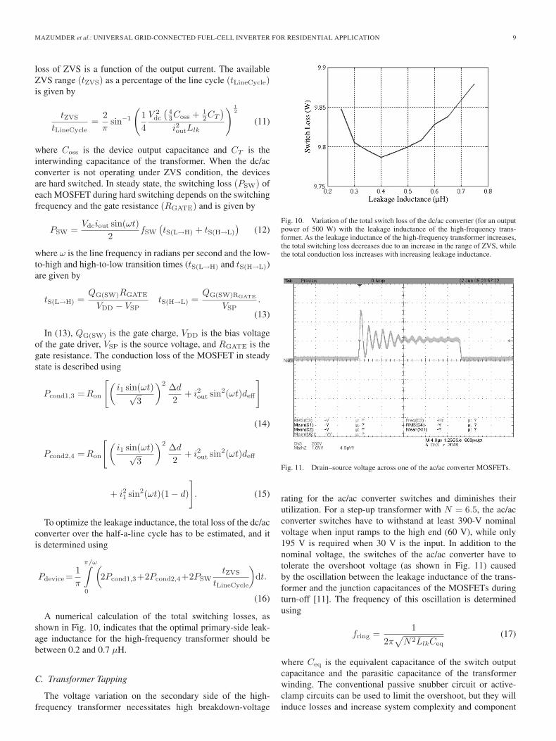
MAZUMDER et al.: UNIVERSAL GRID-CONNECTED FUEL-CELL INVERTER FOR RESIDENTIAL APPLICATION 9
loss of ZVS is a function of the output current. The availableZVS range (tZVS) as a percentage of the line cycle (tLineCycle)is given by
tZVS
tLineCycle=
2π
sin−1
(14
V 2dc
(43Coss + 1
2CT
)i2outLlk
) 12
(11)
where Coss is the device output capacitance and CT is theinterwinding capacitance of the transformer. When the dc/acconverter is not operating under ZVS condition, the devicesare hard switched. In steady state, the switching loss (PSW) ofeach MOSFET during hard switching depends on the switchingfrequency and the gate resistance (RGATE) and is given by
PSW =Vdciout sin(ωt)
2fSW
(tS(L→H) + tS(H→L)
)(12)
where ω is the line frequency in radians per second and the low-to-high and high-to-low transition times (tS(L→H) and tS(H→L))are given by
tS(L→H) =QG(SW)RGATE
VDD − VSPtS(H→L) =
QG(SW)RGATE
VSP.
(13)
In (13), QG(SW) is the gate charge, VDD is the bias voltageof the gate driver, VSP is the source voltage, and RGATE is thegate resistance. The conduction loss of the MOSFET in steadystate is described using
Pcond1,3 =Ron
[(i1 sin(ωt)√
3
)2 Δd
2+ i2out sin2(ωt)deff
]
(14)
Pcond2,4 =Ron
[ (i1 sin(ωt)√
3
)2 Δd
2+ i2out sin2(ωt)deff
+ i21 sin2(ωt)(1 − d)
]. (15)
To optimize the leakage inductance, the total loss of the dc/acconverter over the half-a-line cycle has to be estimated, and itis determined using
Pdevice =1π
π/ω∫0
(2Pcond1,3+2Pcond2,4+2PSW
tZVS
tLineCycle
)dt.
(16)
A numerical calculation of the total switching losses, asshown in Fig. 10, indicates that the optimal primary-side leak-age inductance for the high-frequency transformer should bebetween 0.2 and 0.7 μH.
C. Transformer Tapping
The voltage variation on the secondary side of the high-frequency transformer necessitates high breakdown-voltage
Fig. 10. Variation of the total switch loss of the dc/ac converter (for an outputpower of 500 W) with the leakage inductance of the high-frequency trans-former. As the leakage inductance of the high-frequency transformer increases,the total switching loss decreases due to an increase in the range of ZVS, whilethe total conduction loss increases with increasing leakage inductance.
Fig. 11. Drain–source voltage across one of the ac/ac converter MOSFETs.
rating for the ac/ac converter switches and diminishes theirutilization. For a step-up transformer with N = 6.5, the ac/acconverter switches have to withstand at least 390-V nominalvoltage when input ramps to the high end (60 V), while only195 V is required when 30 V is the input. In addition to thenominal voltage, the switches of the ac/ac converter have totolerate the overshoot voltage (as shown in Fig. 11) causedby the oscillation between the leakage inductance of the trans-former and the junction capacitances of the MOSFETs duringturn-off [11]. The frequency of this oscillation is determinedusing
fring =1
2π√
N2LlkCeq
(17)
where Ceq is the equivalent capacitance of the switch outputcapacitance and the parasitic capacitance of the transformerwinding. The conventional passive snubber circuit or active-clamp circuits can be used to limit the overshoot, but they willinduce losses and increase system complexity and component

10 IEEE TRANSACTIONS ON INDUSTRIAL ELECTRONICS, VOL. 57, NO. 10, OCTOBER 2010
Fig. 12. Peak voltage across the ac/ac converter with varying input voltagefor a transformer primary leakage inductance of 0.7 μH, output capacitance of240 pF (for the devices of the ac/ac converter), and output filter inductance andcapacitance of 1 mH and 2.2 μF, respectively.
Fig. 13. (a) Schematic of the LC filter for standalone operation of the fuel-cell inverter. (b) Phasor diagram describing the relationship among voltages andcurrents of the LC filter. Symbols v′
ac/ac, L′
f , and C′f represent the equivalent
output voltage of the ac/ac converter and the equivalent filter inductance andcapacitance for 120- and 240-V ac output operations.
costs. One simple but effective solution is to adjust the trans-former turns ratio according to the input voltage.
To change the turns ratio of the high-frequency transformer,a bidirectional switch is required. Considering its simplicityand low conduction loss, a low-cost single-pole-double-throw(SPDT) relay is chosen for the inverter prototype, as shown inFig. 3(a) and (b). For this prototype, for an input voltage in therange of 30–42 V, N equals 6.5. Hence, 500-V devices are usedfor the highest input voltage considering an 80% overshoot inthe drain-to-source voltage that was observed in experiments.For an input voltage above 42 V, N equals 4.3, and hence,the same 500-V devices can still be used to cover the highestvoltage as the magnitude of the voltage oscillation is reduced.The relay is activated near the zero-crossing point (where powertransfer is negligible) to reduce the inrush current. Such an
Fig. 14. Two filter designs (along with their respective phasor diagrams) forthe grid-connected inverter using (a) an L and (b) an LCL filter, connectedbetween the inverter and the grid. Symbols v′
ac/ac, L′
f , and C′f represent
the equivalent output voltage of the ac/ac converter and the equivalent filterinductance and capacitance for 120- and 240-V ac output operations. SymbolLf3 represents the inductance between the grid and the inverter.
Fig. 15. Schematics of the converters for (a) the standalone and (b) grid-connected modes of operation. An SPDT relay is used to switch between thetwo modes of operation.

MAZUMDER et al.: UNIVERSAL GRID-CONNECTED FUEL-CELL INVERTER FOR RESIDENTIAL APPLICATION 11
Fig. 16. Schematic of the voltage-mode controller for standalone operation of the inverter.
arrangement improves the efficiency of the transformer andsignificantly increases the utilization of the ac/ac converterswitches for the full range of the input voltage. On the otherhand, without adaptive transformer tapping, the minimal volt-age rating for the devices is given by
Vdcmax · N · (1 + 80%) = 60 · 6.5 · 1.8 = 702 V. (18)
In practice, MOSFETs with 800 V or higher breakdown-voltage ratings are therefore required due to the lack of 700-Vrating devices. The so-called rule of “silicon limit” (i.e., Ron ∝BV 2.5, where BV is the breakdown voltage) indicates that, ingeneral, higher voltage rating MOSFETs will have higher Ron
and hence higher conduction losses. It is noted that the exponentof BV can be different for other power semiconductor devicessuch as CoolMOS. Furthermore, for the same current rating, theswitching speed of a MOSFET with higher breakdown voltagerating is usually slower. As such, if one uses a MOSFET with800 V or higher voltage rating, converter efficiency is expectedto degrade further due to enhanced power loss.
D. Effects of Resonance Between the Transformer LeakageInductance and the Output Capacitance of the AC/ACConverter Switches
Resonance between the transformer leakage inductance andthe output capacitance of the ac/ac converter devices causesthe peak device voltage to exceed the nominal voltage (ob-tained in the absence of the transformer leakage inductance).This is shown in Fig. 12. Considering N = 6.5, one can ob-serve that the peak secondary voltage can be around twicethe nominal secondary voltage. Consequently, the breakdown-voltage rating of the ac/ac converter switches needs to behigher than the nominal value. As MOSFETs are used asswitches, higher breakdown voltage entails increased on re-sistance that yields higher conduction loss. Thus, the leakage
affects the conduction loss and selection of the devices for theac/ac converter.
The resonance begins only after the secondary current com-pletes changing its direction and the ac/ac converter switchesinitiate turn-on or turn-off. During this resonance period, energyis transferred back and forth between the leakage and filterinductances and device and filter capacitances in an almost-lossless manner. The current through the switch, which sup-ports the oscillating voltage, is almost zero. Thus, practically,no switching loss is incurred due to this resonance phenom-enon, although it may have an impact on the electromagnetic-emission profile.
E. Output Filter Design for the Standalone andGrid-Connected Inverter
For the fuel-cell inverter, the design of the output filter iscritical. The filter is so designed such that it mitigates the high-frequency components of the output of the ac/ac converter andgenerates a sinusoidal voltage and current that satisfies thetotal-harmonic-distortion (THD) requirements. For the stand-alone operation of the inverter, we choose a second-order filterwhose phasor diagram is shown in Fig. 13. The value of thefilter inductor is chosen to meet the current ripple requirementaccording to the IEEE 519 standard and is given by [13]
L′f >
18
NVdc
0.2(iout)fSW.
Fig. 13 shows that the current (iC′f) through C ′
f increasesthe reactive power drawn from the converter, which has anadverse effect on the efficiency of the fuel-cell inverter. Thecurrent through the capacitor is given by iC′
f= vout/ωC ′
f ,which shows that, if the capacitance is high, the amount ofreactive current drawn from the inverter increases. The capac-itance design is a tradeoff between the THD requirements andthe tolerable reactive power drawn by the system. To meet the
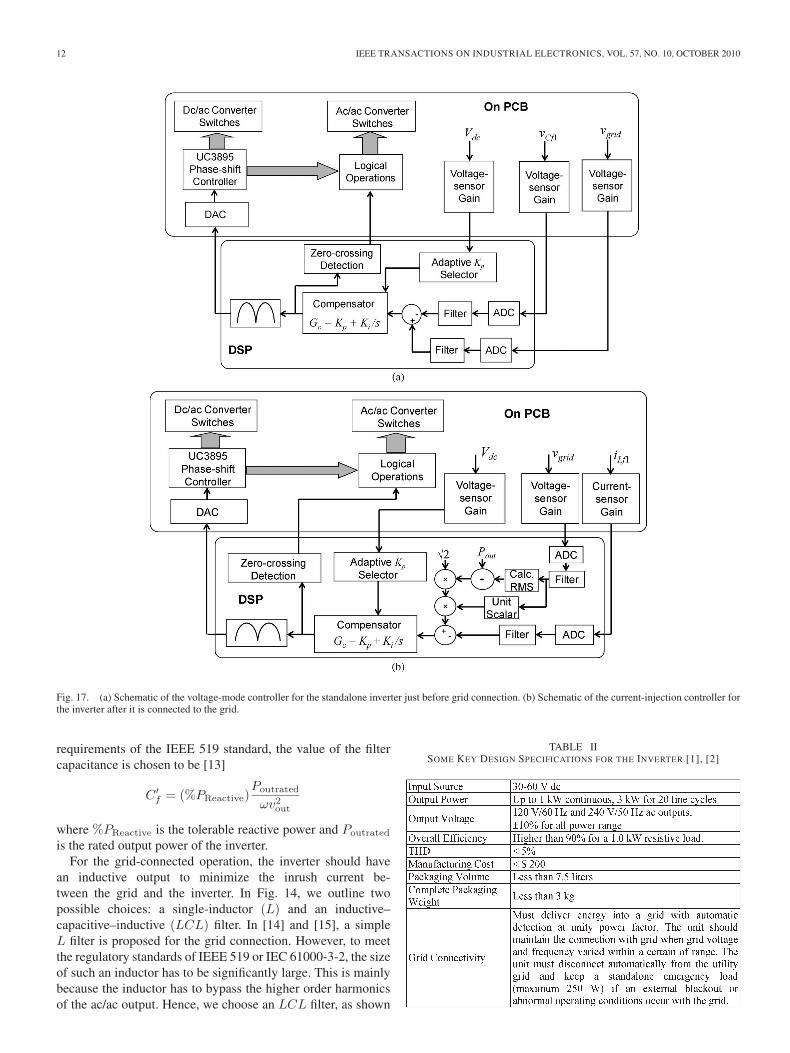
12 IEEE TRANSACTIONS ON INDUSTRIAL ELECTRONICS, VOL. 57, NO. 10, OCTOBER 2010
Fig. 17. (a) Schematic of the voltage-mode controller for the standalone inverter just before grid connection. (b) Schematic of the current-injection controller forthe inverter after it is connected to the grid.
requirements of the IEEE 519 standard, the value of the filtercapacitance is chosen to be [13]
C ′f = (%PReactive)
Poutrated
ωv2out
where %PReactive is the tolerable reactive power and Poutrated
is the rated output power of the inverter.For the grid-connected operation, the inverter should have
an inductive output to minimize the inrush current be-tween the grid and the inverter. In Fig. 14, we outline twopossible choices: a single-inductor (L) and an inductive–capacitive–inductive (LCL) filter. In [14] and [15], a simpleL filter is proposed for the grid connection. However, to meetthe regulatory standards of IEEE 519 or IEC 61000-3-2, the sizeof such an inductor has to be significantly large. This is mainlybecause the inductor has to bypass the higher order harmonicsof the ac/ac output. Hence, we choose an LCL filter, as shown
TABLE IISOME KEY DESIGN SPECIFICATIONS FOR THE INVERTER [1], [2]
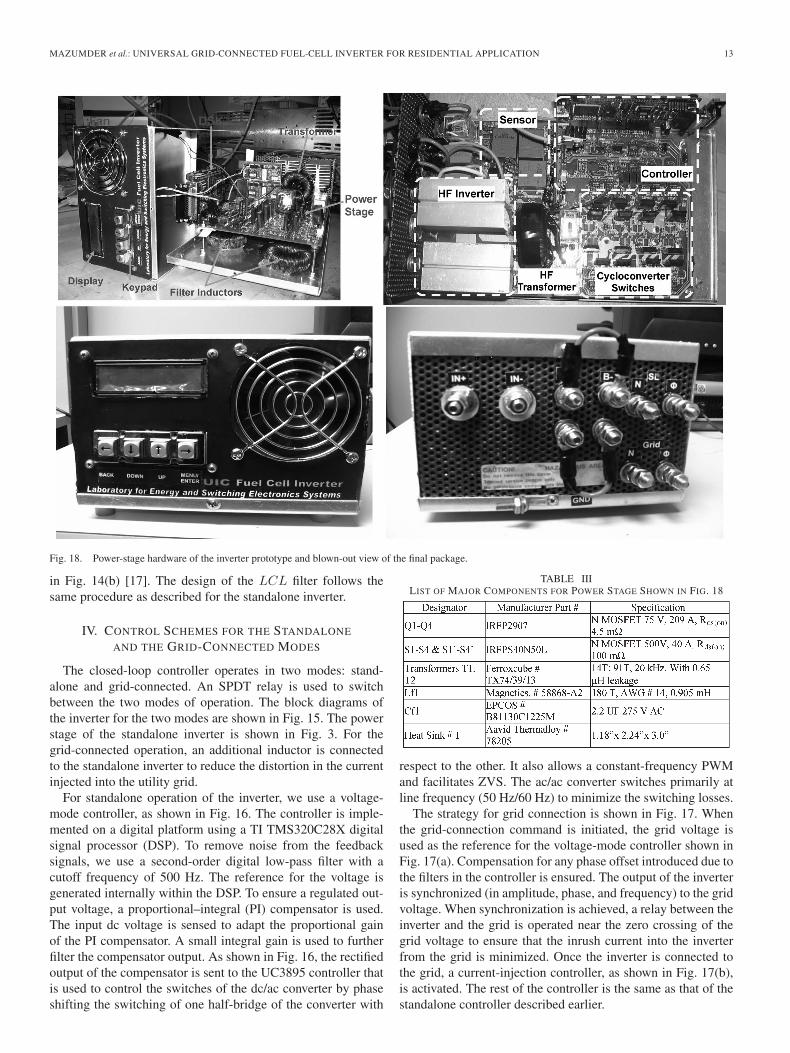
MAZUMDER et al.: UNIVERSAL GRID-CONNECTED FUEL-CELL INVERTER FOR RESIDENTIAL APPLICATION 13
Fig. 18. Power-stage hardware of the inverter prototype and blown-out view of the final package.
in Fig. 14(b) [17]. The design of the LCL filter follows thesame procedure as described for the standalone inverter.
IV. CONTROL SCHEMES FOR THE STANDALONE
AND THE GRID-CONNECTED MODES
The closed-loop controller operates in two modes: stand-alone and grid-connected. An SPDT relay is used to switchbetween the two modes of operation. The block diagrams ofthe inverter for the two modes are shown in Fig. 15. The powerstage of the standalone inverter is shown in Fig. 3. For thegrid-connected operation, an additional inductor is connectedto the standalone inverter to reduce the distortion in the currentinjected into the utility grid.
For standalone operation of the inverter, we use a voltage-mode controller, as shown in Fig. 16. The controller is imple-mented on a digital platform using a TI TMS320C28X digitalsignal processor (DSP). To remove noise from the feedbacksignals, we use a second-order digital low-pass filter with acutoff frequency of 500 Hz. The reference for the voltage isgenerated internally within the DSP. To ensure a regulated out-put voltage, a proportional–integral (PI) compensator is used.The input dc voltage is sensed to adapt the proportional gainof the PI compensator. A small integral gain is used to furtherfilter the compensator output. As shown in Fig. 16, the rectifiedoutput of the compensator is sent to the UC3895 controller thatis used to control the switches of the dc/ac converter by phaseshifting the switching of one half-bridge of the converter with
TABLE IIILIST OF MAJOR COMPONENTS FOR POWER STAGE SHOWN IN FIG. 18
respect to the other. It also allows a constant-frequency PWMand facilitates ZVS. The ac/ac converter switches primarily atline frequency (50 Hz/60 Hz) to minimize the switching losses.
The strategy for grid connection is shown in Fig. 17. Whenthe grid-connection command is initiated, the grid voltage isused as the reference for the voltage-mode controller shown inFig. 17(a). Compensation for any phase offset introduced due tothe filters in the controller is ensured. The output of the inverteris synchronized (in amplitude, phase, and frequency) to the gridvoltage. When synchronization is achieved, a relay between theinverter and the grid is operated near the zero crossing of thegrid voltage to ensure that the inrush current into the inverterfrom the grid is minimized. Once the inverter is connected tothe grid, a current-injection controller, as shown in Fig. 17(b),is activated. The rest of the controller is the same as that of thestandalone controller described earlier.
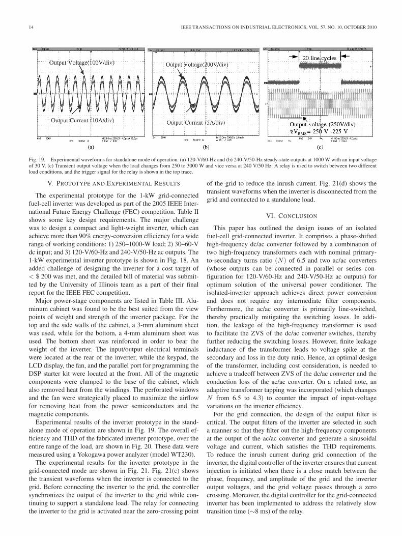
14 IEEE TRANSACTIONS ON INDUSTRIAL ELECTRONICS, VOL. 57, NO. 10, OCTOBER 2010
Fig. 19. Experimental waveforms for standalone mode of operation. (a) 120-V/60-Hz and (b) 240-V/50-Hz steady-state outputs at 1000 W with an input voltageof 30 V. (c) Transient output voltage when the load changes from 250 to 3000 W and vice versa at 240 V/50 Hz. A relay is used to switch between two differentload conditions, and the trigger signal for the relay is shown in the top trace.
V. PROTOTYPE AND EXPERIMENTAL RESULTS
The experimental prototype for the 1-kW grid-connectedfuel-cell inverter was developed as part of the 2005 IEEE Inter-national Future Energy Challenge (FEC) competition. Table IIshows some key design requirements. The major challengewas to design a compact and light-weight inverter, which canachieve more than 90% energy-conversion efficiency for a widerange of working conditions: 1) 250–1000-W load; 2) 30–60-Vdc input; and 3) 120-V/60-Hz and 240-V/50-Hz ac outputs. The1-kW experimental inverter prototype is shown in Fig. 18. Anadded challenge of designing the inverter for a cost target of< $ 200 was met, and the detailed bill of material was submit-ted by the University of Illinois team as a part of their finalreport for the IEEE FEC competition.
Major power-stage components are listed in Table III. Alu-minum cabinet was found to be the best suited from the viewpoints of weight and strength of the inverter package. For thetop and the side walls of the cabinet, a 3-mm aluminum sheetwas used, while for the bottom, a 4-mm aluminum sheet wasused. The bottom sheet was reinforced in order to bear theweight of the inverter. The input/output electrical terminalswere located at the rear of the inverter, while the keypad, theLCD display, the fan, and the parallel port for programming theDSP starter kit were located at the front. All of the magneticcomponents were clamped to the base of the cabinet, whichalso removed heat from the windings. The perforated windowsand the fan were strategically placed to maximize the airflowfor removing heat from the power semiconductors and themagnetic components.
Experimental results of the inverter prototype in the stand-alone mode of operation are shown in Fig. 19. The overall ef-ficiency and THD of the fabricated inverter prototype, over theentire range of the load, are shown in Fig. 20. These data weremeasured using a Yokogawa power analyzer (model WT230).
The experimental results for the inverter prototype in thegrid-connected mode are shown in Fig. 21. Fig. 21(c) showsthe transient waveforms when the inverter is connected to thegrid. Before connecting the inverter to the grid, the controllersynchronizes the output of the inverter to the grid while con-tinuing to support a standalone load. The relay for connectingthe inverter to the grid is activated near the zero-crossing point
of the grid to reduce the inrush current. Fig. 21(d) shows thetransient waveforms when the inverter is disconnected from thegrid and connected to a standalone load.
VI. CONCLUSION
This paper has outlined the design issues of an isolatedfuel-cell grid-connected inverter. It comprises a phase-shiftedhigh-frequency dc/ac converter followed by a combination oftwo high-frequency transformers each with nominal primary-to-secondary turns ratio (N) of 6.5 and two ac/ac converters(whose outputs can be connected in parallel or series con-figuration for 120-V/60-Hz and 240-V/50-Hz ac outputs) foroptimum solution of the universal power conditioner. Theisolated-inverter approach achieves direct power conversionand does not require any intermediate filter components.Furthermore, the ac/ac converter is primarily line-switched,thereby practically mitigating the switching losses. In addi-tion, the leakage of the high-frequency transformer is usedto facilitate the ZVS of the dc/ac converter switches, therebyfurther reducing the switching losses. However, finite leakageinductance of the transformer leads to voltage spike at thesecondary and loss in the duty ratio. Hence, an optimal designof the transformer, including cost consideration, is needed toachieve a tradeoff between ZVS of the dc/ac converter and theconduction loss of the ac/ac converter. On a related note, anadaptive transformer tapping was incorporated (which changesN from 6.5 to 4.3) to counter the impact of input-voltagevariations on the inverter efficiency.
For the grid connection, the design of the output filter iscritical. The output filters of the inverter are selected in sucha manner so that they filter out the high-frequency componentsat the output of the ac/ac converter and generate a sinusoidalvoltage and current, which satisfies the THD requirements.To reduce the inrush current during grid connection of theinverter, the digital controller of the inverter ensures that currentinjection is initiated when there is a close match between thephase, frequency, and amplitude of the grid and the inverteroutput voltages, and the grid voltage passes through a zerocrossing. Moreover, the digital controller for the grid-connectedinverter has been implemented to address the relatively slowtransition time (∼8 ms) of the relay.
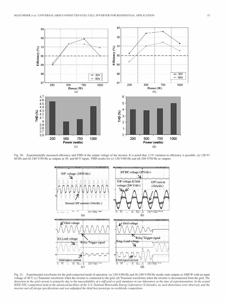
MAZUMDER et al.: UNIVERSAL GRID-CONNECTED FUEL-CELL INVERTER FOR RESIDENTIAL APPLICATION 15
Fig. 20. Experimentally measured efficiency and THD of the output voltage of the inverter. It is noted that ±1% variation in efficiency is possible. (a) 120-V/60-Hz and (b) 240-V/50-Hz ac outputs at 30- and 60-V inputs. THD results for (c) 120-V/60-Hz and (d) 240-V/50-Hz ac outputs.
Fig. 21. Experimental waveforms for the grid-connected mode of operation. (a) 120-V/60-Hz and (b) 240-V/50-Hz steady-state outputs at 1000 W with an inputvoltage of 40 V. (c) Transient waveforms when the inverter is connected to the grid. (d) Transient waveforms when the inverter is disconnected from the grid. Thedistortion in the grid current is primarily due to the unavailability of a stiff grid or grid simulator in our laboratory at the time of experimentation. In the actualIEEE FEC competition held at the advanced facilities of the U.S. National Renewable Energy Laboratory (Colorado), no such distortions were observed, and theinverter met all design specifications and was adjudged the third best prototype in worldwide competition.

16 IEEE TRANSACTIONS ON INDUSTRIAL ELECTRONICS, VOL. 57, NO. 10, OCTOBER 2010
Methodologies for further improvements in the overallenergy-conversion efficiency of the inverter while simultane-ously operating at higher switching frequency (for enhancedpower density), using advanced semiconductor switches andsoft-switching techniques, are being investigated. Extendingthe operation of the single-phase inverter for photovoltaicand battery-based sources as well as for higher power mul-tiphase operation has added foci of our current research anddevelopment.
ACKNOWLEDGMENT
Any opinions, findings, conclusions, or recommendationsexpressed herein are those of the authors and do not necessarilyreflect the views of the National Science Foundation or the U.S.Department of Energy.
REFERENCES
[1] S. K. Mazumder, R. K. Burra, R. Huang, M. Tahir, K. Acharya, G. Garcia,S. Pro, O. Rodrigues, and M. Stasinopoulos, “Single-stage low-cost andenergy-efficient isolated phase-shifted high-frequency inverter followedby a forced cycloconverter for universal residential fuel cell power sys-tem,” in Proc. IEEE Electro/Inf. Technol. Conf., Ames, IA, May 2008,pp. 408–413.
[2] S. Jung, Y. Bae, S. Choi, and H. Kim, “A low cost utility interactiveinverter for residential fuel cell generation,” IEEE Trans. Power Electron.,vol. 22, no. 6, pp. 2293–2298, Nov. 2007.
[3] B. S. Prasad, S. Jain, and V. Agarwal, “Universal single-stage grid-connected inverter,” IEEE Trans. Energy Convers., vol. 23, no. 1, pp. 128–137, Mar. 2008.
[4] H. Tao, J. L. Duarte, and M. A. M. Hendrix, “Line-interactive UPS using afuel cell as the primary source,” IEEE Trans. Ind. Electron., vol. 55, no. 8,pp. 3012–3021, Aug. 2008.
[5] G. K. Andersen, C. Klumpner, S. B. Kjaer, and F. Blaabjerg, “A new greenpower inverter for fuel cells,” in Proc. IEEE Power Electron. Spec. Conf.,2002, vol. 2, pp. 727–733.
[6] R. Gopinath, S. Kim, J. Han, P. N. Enjeti, M. B. Yeary, and J. W. Howze,“Development of a low cost fuel cell inverter system with DSP control,”IEEE Trans. Power Electron., vol. 19, no. 5, pp. 1256–1262, Sep. 2004.
[7] S. K. Mazumder, R. K. Burra, and K. Acharya, “A ripple-mitigating andenergy-efficient fuel cell power-conditioning system,” IEEE Trans. PowerElectron., vol. 22, no. 4, pp. 1437–1452, Jul. 2007.
[8] S. Deng, H. Mao, J. Mazumdar, I. Batarseh, and K. K. J. Islam, “A newcontrol scheme for high-frequency link inverter design,” in Proc. IEEEAppl. Power Electron. Conf., 2003, pp. 512–517.
[9] T. Kawabata, H. Komji, K. Sashida, K. Sanada, and M. Koyama, “Highfrequency link dc/ac converter with PWM cycloconverter,” in Conf. Rec.IEEE IAS Annu. Meeting, 1990, pp. 1119–1124.
[10] M. Matsui, M. Nagai, M. Mochizuki, and A. Nabae, “A high-frequencylink dc/ac converter with suppressed voltage clamp circuits-naturally com-mutated phase angle control with self turn-off devices,” IEEE Trans. Ind.Appl., vol. 32, no. 2, pp. 293–300, Mar./Apr. 1996.
[11] J. A. Sabate and V. Vlatkovic, “Design considerations for high-voltagehigh-power full-bridge zero-voltage-switched PWM converter,” in Conf.Rec. IEEE IAS Annu. Meeting, 1990, pp. 275–284.
[12] K. Wang, F. C. Lee, and W. Dong, “New soft-switched quasi-single-stage (QSS) bi-directional inverter/charger,” in Conf. Rec. IEEE IAS Annu.Meeting, 1999, pp. 2031–2038.
[13] T. C. Y. Wang, Z. Ye, G. Sinha, and X. Yuan, “Output filter design for agrid-interconnected three phase inverter,” in Proc. IEEE Power Electron.Spec. Conf., 2003, pp. 779–784.
[14] M. Ashari, C. V. Nayar, and S. Islam, “Steady-state performance of agrid interactive voltage source inverter,” in Proc. IEEE Power Eng. Soc.Summer Meeting, 2001, vol. 1, pp. 650–655.
[15] Q. Chongming and K. M. Smedley, “Three-phase grid-connected in-verters interface for alternative energy sources with unified constant-frequency integration control,” in Conf. Rec. IEEE IAS Annu. Meeting,2001, pp. 2675–2682.
[16] S. Daher, J. Schmid, and F. L. M. Antunes, “Multilevel inverter topologiesfor standalone PV systems,” IEEE Trans. Ind. Electron., vol. 55, no. 7,pp. 2703–2712, Jul. 2008.
[17] M. Liserre, R. Teodorescu, and F. Blaabjerg, “Stability of grid-connectedPV inverters with large grid impedance variation,” in Proc. IEEE PowerElectron. Spec. Conf., 2004, pp. 4773–4779.
[18] R. Huang and S. K. Mazumder, “A novel soft-switching scheme for anisolated dc/dc converter with pulsating dc output for a three-phase high-frequency-link PWM converter,” in Conf. Rec. IEEE IAS Annu. Meeting,2008, pp. 1–9.
[19] S. K. Mazumder, “A novel hybrid modulation scheme for an isolated high-frequency-link fuel cell inverter,” presented at the IEEE Power Engineer-ing Society Conf., Pittsburgh, PA, Jul., 2008, Invited National ScienceFoundation Panel Paper. [Online]. Available: Paper PESGM2006-000737
[20] S. K. Mazumder, R. K. Burra, R. Huang, and V. Arguelles, “A low-cost single-stage isolated differential Cuk inverter for fuel cell applica-tion,” in Proc. IEEE Power Electron. Spec. Conf., Rhodes, Greece, 2008,pp. 4426–4430.
[21] S. K. Mazumder, T. Sarkar, and K. Acharya, “A directFET based high-frequency fuel-cell inverter,” in Proc. IEEE Appl. Power Electron. Conf.,2009, pp. 1805–1812.
Sudip K. Mazumder (SM’03) received the M.S.degree in electrical power engineering from Rensse-laer Polytechnic Institute, Troy, NY, in 1993 and thePh.D. degree in electrical and computer engineeringfrom Virginia Polytechnic Institute and State Univer-sity, Blacksburg, in 2001.
He is currently the Director of the Laboratoryfor Energy and Switching Electronics Systems, De-partment of Electrical and Computer Engineering,University of Illinois at Chicago, Chicago, where heis also an Associate Professor. He is a Reviewer for
multiple international journals and conferences. He was the Editor-in-Chief forthe International Journal of Power Management Electronics between 2006 and2009. He has over 15 years of professional experience and has held R&Dand design positions in leading industrial organizations. He has publishedover 100 refereed and invited journals and conference papers. His currentareas of interests are interactive power electronics/power networks, renewableand alternate energy systems, photonically triggered and wide-bandgap powersemiconductor devices, and applied technologies.
Dr. Mazumder has been serving as an Associate Editor for the IEEETRANSACTIONS ON INDUSTRIAL ELECTRONICS since 2003 and for the IEEETRANSACTIONS ON AEROSPACE AND ELECTRONIC SYSTEMS since 2008.He was an Associate Editor for the IEEE POWER ELECTRONICS LETTERS
until 2005. He is the Chair of the Student/Industry Coordination Activities forthe IEEE Energy Conversion Congress and Exposition for 2009 and 2010.Since 2009, he has been the Cochair for the IEEE PELS Committee onSustainable Energy Systems and the Vice Chair for the Technical Subcommitteeon Distributed Generation and Renewable Energy. He has been invited bythe IEEE and the American Society of Mechanical Engineers as well asmultiple industries, federal agencies, national laboratories, and universities forseveral keynote, plenary, and invited lectures and presentations. He was therecipient of the prestigious 2008 and 2006 Faculty Research Awards from theUniversity of Illinois for excellent scholarly work and outstanding researchperformance. He was also the recipient of the National Science FoundationCAREER Award and the Office of Naval Research Young Investigator Awardin 2003 and 2005, respectively, and the recipient of the Prize Paper Award fromthe IEEE TRANSACTIONS ON POWER ELECTRONICS and the IEEE PowerElectronics Society (PELS) in 2002. He was also the corecipient of the 2007IEEE Outstanding Student Paper Award at the IEEE International Conferenceon Advanced Information Networking and Applications with Dr. M. Tahir. Hewas also a recipient of the 2005 IEEE Future Energy Challenge Energy Award.
Rajni K. Burra (M’10) received the B.Tech. degreein electronics and communication engineering fromthe Indian Institute of Technology, Kharagpur, India,in 2000 and the M.S. and Ph.D. degrees in elec-trical engineering from the University of Illinois atChicago, Chicago, in 2003 and 2006, respectively.
He is currently a Research Engineer with theGE Global Research Center, Bangalore, India. Hehas published over 13 refereed international journalsand conference papers. His research interests includenonconventional and renewable energy systems, ac-
tive power filtering, and power semiconductor devices.

MAZUMDER et al.: UNIVERSAL GRID-CONNECTED FUEL-CELL INVERTER FOR RESIDENTIAL APPLICATION 17
Rongjun Huang received the B.Eng. and M.Eng.degrees in electrical engineering from JiaotongUniversity, Beijing, China, in 1998 and 2001, respec-tively, and the Ph.D. degree from the Department ofElectrical and Computer Engineering, University ofIllinois at Chicago, Chicago, in 2009.
In 2001, he was an R&D Engineer with HuaweiTechnologies, Shenzhen, China. Currently, he is withInternational Rectifier, San Jose, CA. He has pub-lished over ten refereed international journals andconference papers. His research interests include
power electronics for renewable energy sources, wide-bandgap power semi-conductors, and energy harvesting.
Dr. Huang serves as a Reviewer for the IEEE TRANSACTIONS OF INDUS-TRIAL ELECTRONICS, IEEE TRANSACTIONS ON AEROSPACE AND ELEC-TRONIC SYSTEMS, and several international conferences.
Muhammad Tahir (M’09) received the Ph.D. de-gree in electrical and computer engineering from theUniversity of Illinois at Chicago, Chicago.
Before joining the University of Illinois for hisPh.D., he was a Lecturer with the Department ofElectrical Engineering, University of Engineeringand Technology, Lahore, Pakistan. Between 2008and 2009, he was a Postdoctoral Research Fellowwith the Institute of Microelectronics and WirelessSystems, National University of Ireland, Maynooth,Ireland. Currently, he is an Assistant Professor with
the University of Engineering and Technology. His current research focuseson the area of sensor integration and wireless multimedia sensor networks.His research interests include delay-constrained wireless networks, distributedcommunication network resource optimization, and real-time wireless multi-media networks.
Dr. Tahir was the corecipient of the Outstanding Student Paper Award at the21st IEEE International Conference on Advanced Information Networking andApplications.
Kaustuva Acharya (M’09) received the B.Eng. de-gree in electronics and communication engineeringfrom the Regional Engineering College (now theNational Institute of Technology), Bhopal, India, in2000 and the M.S. and Ph.D. degrees in electrical en-gineering from the University of Illinois at Chicago,Chicago, in 2003 and 2008, respectively.
Between 2003 and 2008, he was a Research Assis-tant with the Laboratory for Energy and Switching-Electronics Systems, University of Illinois atChicago. Subsequently, he was a Postdoctoral Re-
search Associate with the same laboratory between 2008 and 2009 beforeaccepting a position at Texas Instruments. He has published over 20 refereed in-ternational journals and conference papers. His research interests include powerelectronics for renewable and alternate energy sources, and modeling, analyses,and control of interactive power networks for distributed power systems.
Dr. Acharya is a Reviewer for the IEEE TRANSACTIONS ON POWER
ELECTRONICS, IEEE TRANSACTIONS ON INDUSTRIAL ELECTRONICS, andseveral international conferences. He copresented a tutorial entitled “Globalstability methodologies for switching power converters” at the IEEE PowerElectronics Specialists Conference, 2007.