Embed Size (px)
Citation preview

IEEE/ACM TRANSACTIONS ON NETWORKING, VOL. 17, NO. 4, AUGUST 2009 1029
High-Bandwidth Network Memory System ThroughVirtual Pipelines
Banit Agrawal and Timothy Sherwood, Member, IEEE
Abstract—As network bandwidth increases, designing an effec-tive memory system for network processors becomes a significantchallenge. The size of the routing tables, the complexity of thepacket classification rules, and the amount of packet bufferingrequired all continue to grow at a staggering rate. Simply relyingon large, fast SRAMs alone is not likely to be scalable or cost-effec-tive. Instead, trends point to the use of low-cost commodity DRAMdevices as a means to deliver the worst-case memory performancethat network data-plane algorithms demand. While DRAMs candeliver a great deal of throughput, the problem is that memorybanking significantly complicates the worst-case analysis, andspecialized algorithms are needed to ensure that specific types ofaccess patterns are conflict-free.
We introduce virtually pipelined memory, an architectural tech-nique that efficiently supports high bandwidth, uniform latencymemory accesses, and high-confidence throughput even underadversarial conditions. Virtual pipelining provides a simple-to-an-alyze programming model of a deep pipeline (deterministiclatencies) with a completely different physical implementation(a memory system with banks and probabilistic mapping). Thisallows designers to effectively decouple the analysis of their algo-rithms and data structures from the analysis of the memory busesand banks. Unlike specialized hardware customized for a specificdata-plane algorithm, our system makes no assumption about thememory access patterns. We present a mathematical argumentfor our system’s ability to provably provide bandwidth with highconfidence and demonstrate its functionality and area overheadthrough a synthesizable design. We further show that, even thoughour scheme is general purpose to support new applications suchas packet reassembly, it outperforms the state-of-the-art in spe-cialized packet buffering architectures.
Index Terms—Bank conflicts, DRAM, mean time to stall,memory, memory controller, MTS, network, packet buffering,packet reassembly, universal hashing, virtual pipeline, VPNM.
I. INTRODUCTION
W HILE consumers reap the benefits of ever-increasingnetwork functionality, the technology underlying these
advances requires armies of engineers and years of design andvalidation time. The demands placed on a high-throughput net-work device are significantly different than those encountered
Manuscript received August 28, 2007; revised June 17, 2008; approved byIEEE/ACM TRANSACTIONS ON NETWORKING Editor T. Wolf. First publishedMay 29, 2009; current version published August 19, 2009. This work was sup-ported in part by NSF Career Grant CCF-0448654 and NSF-CT-T 0524771.This work is an extended version of the authors’ work in MICRO 39, 2006.
The authors are with the Computer Science Department, University of Cali-fornia, Santa Barbara, Santa Barbara, CA 93106 USA (e-mail: [email protected]; [email protected]).
Color versions of one or more of the figures in this paper are available onlineat http://ieeexplore.ieee.org.
Digital Object Identifier 10.1109/TNET.2008.2008646
in the desktop domain. Network components need to reliablyservice traffic even under the worst conditions [2]–[6], yet theunderlying memory components on which they are built areoften optimized for common-case performance. The problemis that network processing, at the highest throughputs, re-quires massive amounts of memory bandwidth with worst-casethroughput guarantees. A new packet may arrive every 3 nsfor OC-3072, and each packet needs to be buffered, classifiedinto a service class, looked up in the forwarding table, queuedfor switching, rate controlled, and potentially even scannedfor content. Each of these steps may require multiple depen-dent accesses to large irregular data structures such as trees,sparse bit-vectors, or directed graphs, usually from the samememory hierarchy. To make things worse, the size of thesedata structures are continuing to grow significantly, memoryfor buffering has been increasing almost proportionally withthe line rate (40 to 160 Gbps), routing tables have grown from100 to 360 K prefixes, and classification rules have increasedfrom 2000 to 5000 rules in recent years. Network deviceswill become increasingly reliant on high-density commodityDRAM to remain competitive in both pricing and performance.
In this paper, we present virtually pipelined network memory(VPNM), an idea that shields algorithm and processor designersfrom the complexity inherent to commodity memory DRAMdevices that are optimized for common-case performance. Thepipeline provides a programming model and timing abstractionthat greatly eases analysis. A novel memory controller upholdsthat abstraction and handles all the complexity of the memorysystem, including bank conflicts, bus scheduling, and bursts ofaccesses to the exact same address. This frees the programmerfrom having to worry about any of these issues, and the memorycan be treated as a flat, deeply pipelined memory with fully de-terministic latency no matter what the memory access pattern is(Fig. 1). Building a memory controller that can create such anillusion requires that we solve several major problems:
• Multiple conflicting requests: Two memory requests thataccess the same bank in memory will be in conflict, andwe will need to stall at least one request. To hide these con-flicts, our memory controller uses per-bank queues alongwith a randomized mapping to ensure that independentmemory accesses have a statistically bounded number ofbank conflicts. (Sections III-B and IV-A2)
• Reordering of requests: To resolve bank conflicts, re-quests need to be reordered, but our virtual pipelinepresents a deterministic (in-order) interface. The latenciesof all memory accesses are normalized through special-ized queues, and accesses are reordered in a distributed(per-bank) manner to create the appearance of fullypipelined memory. (Sections III-C and IV-A4)
1063-6692/$26.00 © 2009 IEEE
Authorized licensed use limited to: MICROSOFT. Downloaded on April 15,2010 at 20:22:58 UTC from IEEE Xplore. Restrictions apply.

1030 IEEE/ACM TRANSACTIONS ON NETWORKING, VOL. 17, NO. 4, AUGUST 2009
Fig. 1. High-level block diagram of virtual pipeline where each access toDRAM is normalized to a deterministic latency (D).
• Redundant requests: As repeated requests for the same datacannot be randomized to different banks, normalizing thelatency for these requests could create the need for giganticqueues. Instead, we have built a novel form of mergingqueues that combines redundant requests and acts as acache but provides data playback at the right times to main-tain the illusion of a pipeline. (Sections III-D and IV-A1)
• Worst-case analysis: In addition to the architectural chal-lenges listed above, reasoning about the worst-case be-havior of our system requires careful mathematical anal-ysis. We show that it is provably hard for even a perfectadversary to create stalls in our virtual pipeline with greatereffectiveness than random chance. (Sections V-B and V-C)
To quantify the effectiveness of our system, we have per-formed a rigorous mathematical analysis, executed detailed sim-ulation, created a synthesizable version, and estimated hard-ware overheads. In order to show that our approach will actu-ally provide both high performance and ease of programming,we have implemented a packet buffering scheme as a demon-stration of performance and a packet reassembler as a demon-stration of usefulness, both using our memory system. We showthat, despite the generality of our approach (it does not assumethe head-read, tail-write property) it compares favorably withseveral special-purpose packet buffering architectures in bothperformance and area (Section VI).
II. RELATED WORK
Dealing with timing variance in the memory system hascertainly been addressed in several different ways in the past.Broadly, the related work can be broken up into two groups:scheduling and bank conflict reduction techniques that work inthe common case, and special purpose techniques that aim toput bounds on worst-case performance for particular classes ofaccess patterns.
Common-case DRAM Optimizations: Memory bankconflicts not only effect the total throughput available froma memory system; they can also significantly increase thelatency of any given access. In the traditional processing do-main, memory latency can often be the most critical factorin terms of determining performance, and several researchershave proposed hiding this latency with bank-aware memorylayout, prefetching [7], and other architectural techniques[8]–[11]. While latency is critical, traditional machines are farmore tolerant of nonuniform latencies and reordering becausemany other mechanisms are in place to ensure the proper
execution order is preserved. For example, in the streamingmemory controller (SMC) architecture, memory conflicts arereduced by servicing a set of requests from one stream beforeswitching to a different stream [12]. A second example is thememory scheduling algorithm, where memory bandwidth ismaximized by reordering various command requests [13]. Inthe vector processing domain [14], a long stream requiresconflict-free access for larger number of strides. Rau et al. [15]use randomization to spread the accesses around the memorysystem and, through the use of Galois fields, show that it ispossible to have a pseudorandom function that will work aswell on any possible stride. While address mapping such asskewing or linear transformations can be used for constantstride, out-of-order accesses can efficiently handle a largernumber of strides [16]. Corbal et al. [17] present a commandvector memory system (CVMS) where a full vector request issent to the memory system instead of individual addresses toprovide higher performance.
While these optimizations are incredibly useful, industrial de-velopers working on devices for the core will not adopt them dueto the fact that certain deterministic traffic patterns could causeperformance to sink drastically. Dropping a single packet canhave an enormous impact on network throughput (as this causesa cascade of events up the network stack), and the customerneeds to be confident that the device will uphold its line rate. Inthis domain, it would be ideal if there were a general-purposeway to control banked access such that conflicts never occur.Sadly, this is not possible in the general case [18]. However, ifthe memory access patterns can be carefully constrained, algo-rithms can be developed that solve certain special cases.
Removing Bank Conflicts in Special Cases: One of themost important special cases that has been studied is packetbuffering. Packet buffering is one of the most memory-inten-sive operations that networks need to deal with [3], [4], andhigh-speed DRAM is the only way to provide both the den-sity and performance required by modern routers. However, inrecent years, researchers have shown special methods for map-ping these packet buffer queues onto banks of memory such thatconflicts are either unlikely [6], [19], [2], [20] or impossible [4],[3]. These techniques rely on the ability to carefully monitor thenumber of places in memory where a read or write may occurwithout a bank conflict and to schedule memory requests aroundthese conflicts in various ways. For example, in [4], a specializedstructure similar to a reorder buffer is used to schedule accessesto the heads and tails of the different packet buffer queues. Thetechnique combines clever algorithms with careful microarchi-tectural design to ensure worst-case bounds on performanceare always met in the case of packet buffering. Randomiza-tion has also been considered in the packet buffering space. Forexample, Kumar et al. present a technique for buffering largepackets by randomly distributing parts of the packet over manydifferent memory channels [21]. However, this technique canhandle neither small packets nor bank conflicts. Another impor-tant special case is data-plane algorithms that may also sufferfrom memory-bank conflict concerns. Whether these banks ofmemory are on- or off-chip, supporting multiple nonconflictingbanked memory accesses requires a significant amount of anal-ysis and planning. For example, a conflict-reduced tree-lookupengine was proposed by Baboescu et al. [22]. A tree is brokeninto many subtrees, each of which is then mapped to parts of a
Authorized licensed use limited to: MICROSOFT. Downloaded on April 15,2010 at 20:22:58 UTC from IEEE Xplore. Restrictions apply.

AGRAWAL AND SHERWOOD: HIGH-BANDWIDTH NETWORK MEMORY SYSTEM THROUGH VIRTUAL PIPELINES 1031
rotating pipeline. They prove that optimally allocating the sub-trees is NP-complete and present a heuristic mapping instead.Similarly in [23], a conflict-free hashing technique is proposedfor longest prefix match (LPM), where conflicts are handled atan algorithmic level. While the above methods are very pow-erful, they all require careful layout (by the programmer or hard-ware designer) of each data structure into the particular bankstructure of the system and allow neither changes to the datastructures nor sharing of the memory hierarchy.
While our approach may have one stall on average once everycycles (on the order of hours), the benefit is that no time
has to be spent considering the effect of banking on already-complex data structures. As we will describe in Section III,a VPNM system uses cryptographically strong randomization,several new types of queues, and careful probabilistic analysisto ensure that deterministic latency is efficiently provided withprovably strong confidence.
III. VIRTUALLY PIPELINED MEMORY
Vendors need to have confidence that their devices will op-erate at the advertised line rates regardless of operating con-ditions, including when under denial of service attack by ad-versaries or in the face of unfortunate traffic patterns. For thisreason, most high-end network ASICs do not use any DRAMfor data-plane processing because the banks make worst-caseanalysis difficult or impossible. The major exception to this ruleis packet buffering; even today, it requires an amount of memorythat can only be satisfied through DRAM, and a great deal of ef-fort has been expended to map packet-buffering algorithms intobanks with worst-case bounds. Later in Section VI-A, we com-pare our implementation against several special-purpose archi-tectures for packet buffering.
A. Dram Banks
Modern DRAM designs try to expose the internal bankstructure so accesses can be interleaved and the effectivebandwidth can be increased [24], [25]. The various types ofDRAM differ primarily in their interfaces at the chip and buslevel [26]–[28], but the idea of banking is always there. Experi-mental evidence [28] indicates that on average PC133 SDRAMworks at 60% efficiency and DDR266 SDRAM works at 37%efficiency, where 80%–85% of the lost efficiency is due to thebank conflicts. To help address this problem, RDRAMs exposemany more banks [28]. For example, in Samsung RambusMR18R162GDF0-CM8, each RDRAM device can contain upto 32 banks, and each RIMM module can contain up to 16such devices, so the module can have up toindependent banks [29].
A bank conflict occurs when two accesses require differentrows in the same bank. Only one can be serviced at a time, andhence, one will be delayed by time steps. is the ratio ofbank access time to data transfer time; in other words, it is thenumber of accesses that will have to be skipped before a bankconflict can be resolved. Throughout this paper, we conserva-tively assume that there is one transfer per cycle, and we selectthe value of [29], [30]. If is smaller, then our approachwill be even more efficient. Besides bank conflicts, DRAM isalso unavailable for incoming requests during the refresh oper-ation. However, there are techniques such as concurrent refresh
[31], where refresh operation can be done simultaneously withread/write operation and, with further optimizations, unavail-ability due to refresh operation could be eliminated.
B. Building a Provably Strong Approach
To prove that our approach will deliver throughput with highconfidence, we consider the best possible adversary and showthat such an adversary can never tractably construct a sequenceof accesses that performs poorly. First, we map the data to banksin permutations that are provably as good as random. Universalhashes [32], an idea that has been extended by the cryptographycommunity, provide a way to ensure that an adversary cannotfigure out the hash function without direct observation of con-flicts. These hashing techniques are very similar to block ci-phers, although the complexity is significantly reduced. This re-duction comes from the fact that a universal hash only needs tooutput bits for banks, as opposed to the 64- or 128-bitoutputs required from a block cipher. While a strong crypto-graphic hash ensures that collisions are impossible for an adver-sary to discover (which necessarily requires a very large range),a universal hash (which works over small ranges, such as thenumber of banks in our system) only ensures that collisions donot occur with greater than uniformly random probability.
For bank mapping, we need perfect universal hashing in thesense that it needs to appear perfectly random (not perfectlybalanced), and universal hashing provides this guarantee. Therecould be a chance that we get unlucky and all accesses mightresult in bank conflicts, but this is true in the same way that ahacker might get lucky and guess a cryptographic key on the firsttry. The probability of this happening even when an attacker istrying very hard is what is important, and that can be signifi-cantly lowered if there is no direct observation of conflicts. Thevirtual pipeline provides exactly this functionality and preventsan adversary from seeing those conflicts through specializedqueues. This latency normalization not only allows us to for-mally reason about our system; it also shields the processor fromthe problem of reordering and greatly simplifies data structureanalysis. While the latency of any given memory access will beincreased significantly over the best possible case, the memorybandwidth delivered by the entire scheme is almost equal to thecase where there are no bank conflicts. While this may makelittle sense in the latency-intolerant world of desktop computing,this can be a huge benefit in the network space.
C. Distributed Scheduling Around Conflicts
While universal hashing provides the means to prevent ourtheoretical adversary from constructing access sequences thatresult in more conflicts than a randomly generated sequence,even in a random assignment of data to banks, a relatively largenumber of bank conflicts can occur due to the Birthday Paradox[33]. In fact, if there was no queuing used, then it would takeonly accesses before the first stall would occur if thereare banks. Clearly, we will need to schedule around theseconflicts in order to keep the virtual pipeline timing abstraction.In our implementation, a controller for each bank is used, andeach bank handles requests in order, but each bank is handledindependently, so the requests to different banks may be handledout of order. Each bank controller is then in charge of ensuringthat for every access at time , it returns the result at timefor some fixed value of . As long as this holds, there is no
Authorized licensed use limited to: MICROSOFT. Downloaded on April 15,2010 at 20:22:58 UTC from IEEE Xplore. Restrictions apply.

1032 IEEE/ACM TRANSACTIONS ON NETWORKING, VOL. 17, NO. 4, AUGUST 2009
Fig. 2. An example of how each bank controller will normalize the latency of memory accesses to a fixed delay �� � ���. In all three graphs, the x-axis is cycles,and each memory access is shown as a row. The light white boxes are the times during which the request is “in the pipeline,” while the dark gray box is the actualtime that it takes to access the bank �� � ���. In this way, a certain number of bank conflicts can be hidden as long as there are not too many requests in a shortamount of time. The graph on the left shows normal operation, while the middle graph shows what happens when there are redundant requests for a single bank,which therefore do not require bank access. The graph on the right shows what happens when there are too many requests to one bank (A–E) in a short period oftime, thus causing a stall. Later in the analysis section, we will also refer to�, which is the maximum number of overlapping requests that can be handled. In thiscase, � is ����� � �.
need for the programmer to worry about the fact that there iseven such a thing as banks.
One major benefit of our design is that the memory sched-uling and reordering can be done in a fully parallel and indepen-dent manner. If each memory bank has its own controller, thereis exactly one request per cycle, and each controller ensures thatthe result of a request is returned exactly cycles later, thenthere is no need to coordinate between the controllers. When itcomes to return the result at time , a bank controller willknow that it is always safe to send the data to the interface be-cause, by definition, it was the only one to get a request at time .
D. What Can Go Wrong
If there are banks in the system, then any one bank willonly have a 1 in chance of getting a new request on any givencycle.1 The biggest thing that can go wrong is that we get somany requests to one bank that one of the queues fills up and weneed to stall. Reducing the probability of this happening evenfor the worst-case access pattern requires careful architecturaldesign and mathematical analysis. In fact, there are two ways abank can end up getting more than of the requests.
The first way is that it could be unlucky, and just due to ran-domness, more than of the requests go to a single bank (be-cause we map them randomly). By keeping access queues, wecan ensure that the latency is normalized to to handle simulta-neously occurring bank conflicts. How large that number is andhow long it will take to happen in practice are discussed exten-sively in Section V. In practice, we find that normalizing toabout 1000 ns is more than enough and is also several orders ofmagnitude less than a typical router processing latency of 0.5 to2 ms [34]. While this a typical example, the actual value of isdependent on and the size of bank access queue, as describedin Section IV. While there is a constant added delay to due touniversal hashing, the hash function can be fully pipelined, andthen it will not be any big impact to the normalized delay .
The second way we could get many accesses to one bank isthat there could be repeated requests for the same memory line.The invariant that a request at time is satisfied at time
1This is not to say that each bank will be responsible for exactly ��� of therequests as in round-robin. Round-robin will not work here because each requestmust be satisfied by the one bank that contains its memory. Although we get topick the mapping between memory lines and banks, the memory access patternwill determine which actual memory lines are requested.
Fig. 3. Memory controller block diagram. After an access is mapped to theproper bank by the universal hash engine �� �, it is sent to the correspondingbank controller for further processing.
must hold for this case as well, and in Section V-C, we describehow to design a special merging queue to address this secondproblem. The idea behind our merging queue is that redundantmemory accesses are combined into a single access and a singlequeue entry internally. If an access A comes at and a redun-dant access A comes at , a reply still needs to be made atand at even though internally only one queue entry forA is maintained. In addition to handling the repeating pattern“A,A,A,A, ,” we need to handle “A,B,A,B, ” with only twoqueue entries. In fact, if we need to handle bank conflictswithout a stall, then we will need to handle up to differentsets of redundant accesses. In Fig. 2, we show how the VPNMworks altogether for different type of accesses.
IV. IMPLEMENTING THE INTERFACE
At a high level, the memory controller implementing ourvirtual pipeline interface is essentially a collection of decoupledmemory bank controllers. Each bank controller handles onememory bank or one group of banks that act together as a singlelogical bank. Fig. 3 shows one possible implementation where amemory controller contains all of the bank controllers on-chip,and they all share one bus. This would require no modificationto the bus or DRAM architecture.
The performance of our controller is limited by the singlebus to the memory banks. If we have to service one memoryrequest per cycle, then we need to have one outgoing accesson each cycle to the memory bus, and the bus will become a
Authorized licensed use limited to: MICROSOFT. Downloaded on April 15,2010 at 20:22:58 UTC from IEEE Xplore. Restrictions apply.

AGRAWAL AND SHERWOOD: HIGH-BANDWIDTH NETWORK MEMORY SYSTEM THROUGH VIRTUAL PIPELINES 1033
bottleneck. Hence, to keep up with the incoming address percycle and to prevent any accumulation of requests in the bankcontroller due to mismatched throughputs, we need to support aslightly higher number of memory bus transactions per secondthan allowed on the interface bus. We call the ratio of the requestrate on the interface bus and request rate of memory bus as busscaling ratio . The value of ‘R’ is chosen slightly higherthan 1 to provide slightly higher access rate on the memory sidecompared to the interface side. This mismatch ensures that idleslots in the schedule do not accumulate slowly over time. Around-robin scheduler arbitrates the bus by granting access toeach bank controller every cycles, where is the numberof banks. It might happen that some of the round-robin slotsare not used when there is no access for the particular bank orthe memory bank is busy, although with further analysis or asplit-bus architecture, this inefficiency can be eliminated.
After the determination of which bank a particular memoryrequest needs to access, the request is handed off to the appro-priate bank controller that handles all the timing and schedulingfor that one bank. Almost all of the latencies in the system arefully deterministic, so there is no need to employ a complicatedscheduling mechanism. The only time the latencies are not fullydeterministic is when there are a sufficient number of memoryaccesses to a single bank in a sufficiently small amount of timethat cause the latency normalizing technique to stall. However,as we will show in Section V, the parameters of the architecturecan be chosen such that this happens extremely infrequently (onthe order of once every trillion requests in the worst case).
Since stalls happen so infrequently and the stall time is alsovery low (in the worst case, a full memory access latency), stallscan be handled in one of two ways. The first way is to simplystall the controller, where the slowdown would not even be afraction of a percent, while the other alternative is to simply dropthe packet (which would be noise compared to packet-loss dueto many other factors). In either case, an attacker cannot leverageinformation about a stall unless they can: 1) observe the exactinstant of the stall; 2) remember the exact sequence of accessesthat caused the stall; and 3) replay the stall-causing events withminor changes (to look for more multiple collisions). With ran-domization due to universal mapping and a very high value ofmean time to stall (around , as described in Sections V-Band V-C), the ability to do this will be practically impossible.If such attacks are believed to be a threat, a further (and sightlymore costly) option is to change the universal mapping functionand reorder the data on the occurrence of multiple stalls (an ex-pensive operation but certainly possible with frequency on theorder of once a day).
A. Bank Controller Architecture
Solving the challenges described in Section I requires a care-fully designed bank controller. In particular, it must be able toqueue the bank requests, store the data to a constant delay, andhandle multiple redundant requests.
The architecture block diagram of our bank controller isshown in Fig. 4. From the figure, we can see that the bankcontroller consists of five main components described with thetext next to each block. The primary tasks of these componentsinclude queuing input requests, initiating a memory request,and sending data to the interface at a prespecified time slot toensure the deterministic latency, and each of these components
is designed to address one or more of the challenges men-tioned earlier. We now describe each of these components indetail.
1) Delay Storage Buffer: The delay storage buffer stores theaddress of each pending and accessing request and stores the ad-dress and data of waiting requests. Each nonredundant requestwill have an entry allocated for it in the delay buffer for a totalof cycles. To account for repeated requests to the same ad-dress, we associate a counter with each address and data. An in-crementer/decrementer is associated with each counter to keeptrack of the number of unserviced requests for the correspondingaddress. The buffer contains rows, where each row containsan address of bits, a 1-bit address valid flag, a counter ofbits, and data words of bits. The number of rows playsa pivotal role in deciding the stall rate of the system, which wediscuss in detail in Section V-B. and can be assigned anydesign-specific values, whereas the value of depends on theoverall deterministic latency . It should be at least(for bits). A row is called free when thecounter of that row is zero. A first-zero circuit finds out the firstfree row. The free row gets assigned to a new read request, andthe address is written to the address content addressable memory(CAM). The free row is updated using the first-zero circuit atthe same time. The data words are buffered in the specifiedrow whenever the read access to memory bank completes. Thebuffering of data words in delay storage buffer ensures that wecan handle repeated requests to the same address and can pro-vide the data words to the interface side after a deterministiclatency .
2) Bank Access Queue: The bank access queue keeps trackof all pending read and write requests that require access to thememory bank. It can store up to interleaved read or writerequests in FIFO order. The value of is also crucial to dic-tate the stall rate of the system, which we discuss in detail inSection V-C. To minimize the area overhead, we just keep a fewbits to store the requests. There is 1 bit per entry to specify thetype of access, i.e., whether the request is a read or write request.The remaining bits per entry are used only in the case ofread accesses to specify the corresponding row in delay storagebuffer (that way we do not require duplicate copy of address).
3) Write Buffer: The write buffer is organized as a FIFOstructure, which stores the address and data of all incoming writerequests. Unlike read requests, we do not need to wait for thewrite requests to complete. We only need to buffer each writerequest until it gets scheduled to access the memory bank. Thewrite buffer can contain a maximum of write requests, whereeach request row consists of bits of address and bits ofdata. In our case, the value of is chosen as , assumingequal read and write operations (to make a close comparison topacket buffering).
4) Circular Delay Buffer: The circular delay buffer storesthe request identifier (id) of every incoming read request inSRAM memory. Then, the read request is served to the outputinterface after the deterministic latency . Hence, we needa FIFO of length , where. on one end. the request identifier(which specifies a row in delay storage buffer) for new read re-quests is added and, on the other end, the request identifier isread to serve the data to the output interface. This operationrequires one read port and one write port in SRAM memory.Hence, two-ported memory design increases the area overhead
Authorized licensed use limited to: MICROSOFT. Downloaded on April 15,2010 at 20:22:58 UTC from IEEE Xplore. Restrictions apply.

1034 IEEE/ACM TRANSACTIONS ON NETWORKING, VOL. 17, NO. 4, AUGUST 2009
Fig. 4. Architecture block diagram of the VPNM bank controller.
and power consumption. This circular delay buffer is the onlycomponent that is accessed every cycle irrespective of the inputrequests. This problem motivates the design of our 2-set SRAMarchitecture, where in and out pointers are used for writing andreading, respectively. The size of each SRAM set is , andthe width of each set entry is bits. The valid bit is1 bit to signify any valid read requests appeared in that cycle,whereas bits represent the encoded row id of a row indelay storage buffer. Note that if we just stored the full datahere, instead of a pointer to the delay storage buffer, then wewould need to have a huge number of bytes to buffer all the data(2 to 3 orders of magnitude more).
As we have to provide a fixed latency of cycles betweenan in operation and an out operation, the write pointer in chases
the read pointer out by exactly one cycle delay.} This in pointerchasing accounts for delay. Then, we latch the outputdata for one more cycle to achieve deterministic latency .The two-set architecture requires only one read-write port, andboth sets can be accessed in parallel (one for in operation and theother for out operation). This reduces the overall delay and pro-vides considerable energy and area savings. A sample of pointerswitching with different time of accesses is shown in the twosets of circular delay buffer in Fig. 4. The end result is that thisbuffer lets us normalize the latency to very efficiently.
5) Control Logic: The control logic handles the necessarycommunication between components. (While the interconnectinside the bank controller is drawn as a bus for simplicity, infact it is a collection of direct point-to-point connections.) The
Authorized licensed use limited to: MICROSOFT. Downloaded on April 15,2010 at 20:22:58 UTC from IEEE Xplore. Restrictions apply.
AGRAWAL AND SHERWOOD: HIGH-BANDWIDTH NETWORK MEMORY SYSTEM THROUGH VIRTUAL PIPELINES 1035
control logic also controls the interface-side request handlingand memory-side request scheduling. It keeps an encoded readrow for which the memory is currently being accessed so that,on the completion of the request, the data can be written to thisrow in delay storage buffer. It also invalidates the in entry inthe circular delay buffer in case there is no read request in thecurrent cycle.
B. Controller Operations
At a high level, each memory request goes through fourstates: pending, accessing, waiting, and completed. New re-quests start out as pending, and when the proper request isactually sent out to the DRAM, the request is accessing. Whenthe result returns from DRAM the request is waiting (untiltotal cycles have elapsed), and finally the request is completedand results are returned to the rest of the system.
When a new read request comes in, all the valid addressesof the address CAM in the delay storage buffer are searched.On a match (a redundant access), the matched row counter isincremented, and the id of the matched row is written to thecircular delay buffer (along with its valid bit). On a mismatch,a free row is determined using the first zero circuit and is up-dated with the new address, and the counter is initialized to one.The id of the corresponding free row is written to the circulardelay buffer. During this mismatch case, we also add the row idcombined with ‘0’ bit (read) to the bank access queue (where itwaits to become accessing). On an incoming write request, thewrite address and data is added to write buffer (FIFO). A ‘1’ bit(write) is written to the bank access queue. The row id is un-used in this case as we access the write buffer in FIFO order. Itis also searched in the address CAM, and on a match, the ad-dress valid flag is unset. However, this row cannot be used fora new read request until all previous read requests are servicedand the counter reaches zero because the data until the currentcycle is still valid. When the counter reaches zero, then there areno pending requests for that row, and the row can serve as freerow for the new requests.
During each cycle, the controller scans the bank access queueand reads from the circular delay buffer. If the bank controller isgranted to schedule a memory bank request, then the first requestin the bank access queue is dequeued for access. In the case ofa read access, the address is read from the delay storage bufferand put on the memory bank address bus. In the case of writeaccess, the address and the data words are dequeued from thewrite buffer, and the write command is issued to the memorybank. In the case of no incoming read requests in the currentcycle, the control logic invalidates the current entry of circulardelay buffer. On every cycle, it also reads the -cycle delayedrequest id from the circular delay buffer. If it is valid, then thedata is read from the data words present in delay storage buffer,and the data is put on the interface bus.
C. Stall Conditions
The aim of the VPNM bus controller architecture is to providea provably small stall rate in the system through randomization,but the actual stall rate is a function of the parameters of thesystem. There are three different cases that require a stall toresolve, each of which is influenced by a different subset of theparameters.
TABLE IPARAMETERS FOR THE ANALYSIS OF OUR CONTROLLER
1) Delay storage buffer stall: The number of rows indelay storage buffer are limited, and a row has to be re-served for cycles for one data output. Hence, if thereare no free rows and it cannot reserve a row for a newread request, then it results in a delay storage buffer stall.This stall is mainly dependent on the following parame-ters: a) number of rows in delay storage buffer; b) de-terministic delay ; and c) number of banks . Thedeterministic delay is determined using the access latency
and the bank request queue size , and this stall anal-ysis is presented in Section V-B.
2) Bank access queue stall: When a new nonrepeating read/write request comes to a bank and the size of the bankaccess queue is already , then the new request cannotbe accommodated in the queue. This condition results inbank access queue stall. There are three main parametersthat control this stall: a) average input rate, which is equalto , where is the number of banks; b) queue size
; and c) the output rate, which is decided by the ratioof frequency on the memory side and frequency on the
interface side. In Section V-C, we discuss exactly how toperform the confidence analysis for this stall.
3) Write buffer stall: Write buffer (WB) stall happens whena write request cannot be added in the write buffer. As wekeep the write buffer equal to half of the bank access queuesize, the chances of stall rate in write buffer are much lessthan the stall rate in bank access queue. The analysis of thewrite buffer stall is similar to the analysis of bank accessqueue and does not dominate the overall stall, so we willonly discuss the bank access queue and delay storage bufferstall in our mathematical analysis in Section V.
V. ANALYSIS OF DESIGN
The VPNM can stall in the three ways described inSection IV-C. In any of these cases, the buffer will haveto stall, and it will not be able to take a new request that cycle.Because we randomize the mapping, we can formally analyzethe probability of this happening. Additionally, because we usethe cryptographic idea of universal hashing, we know that thereis no deterministic way for an adversary to generate conflictswith greater than random probability unless they can directlysee them. We ensure that the conflicts are not visible throughlatency normalization (queuing both before and after a request)unless many different combinations are tried. We quantify thisnumber, and the confidence we place in our throughput, as themean time to stall (MTS). It is important to maximize the MTS,a job we can perform through optimization of the parametersdescribed in Section IV and summarized in Table I.
To evaluate the effect of these parameters on MTS, we per-formed three types of analysis: simulation (for functionality),
Authorized licensed use limited to: MICROSOFT. Downloaded on April 15,2010 at 20:22:58 UTC from IEEE Xplore. Restrictions apply.
1036 IEEE/ACM TRANSACTIONS ON NETWORKING, VOL. 17, NO. 4, AUGUST 2009
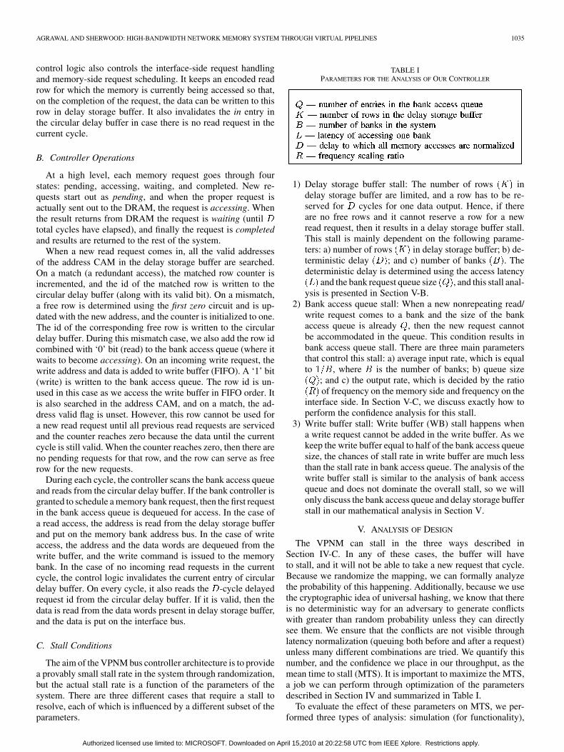
Fig. 5. Bank request controller simulation using ���� ���, and �����.
mathematical (for MTS), and design (to quantify the hardwareoverhead). To get an understanding of the execution behavior ofour design and verify our mathematical models, we have builtfunctional models in both C and Verilog and synthesized ourdesign using synopsys design compiler. However, in this paper,we concentrate on the mathematical analysis of delay storagebuffer stall and bank access queue stall, the calculation of theMTS for both these cases, the effect of normalized delay, and ahigh-level analysis of the hardware required.
A. Simulation of the Design
As described earlier, the number of rows in a delay storagebuffer and the size of bank access queue are important designparameters to decide the stall rate of the system. In this section,we present a simple simulation with random accesses just toprovide a look into the intuition behind our approach. Fig. 5shows the resource utilization over time for one bank controller.In this illustration, the number of banks is 128, the number ofrows in delay storage buffer is 8, and bank access queue sizeis 4. The top bar shows the arrival of requests to the controller,which is a random process. The utilization of the two criticalresources described above are in the lower two graphs. As seen,in the window of 2200–2300 cycles, a burst of requests comesto the controller and almost fills the bank access queue, and fourrows are reserved in the delay storage buffer. Subsequently, thenumber of busy rows and pending entries decrease because inputburst requests are serviced, and there is no new incoming requestfor some time. We could have seen a stall in a case when a burstof requests arrive in short time such that it fills up either thedelay storage buffer or the bank access queue. However, queue/buffer parameters are large enough in this case to not witnesssuch a stall. In the next sections, we see how these architecturalparameters effect the stall rate through a detailed mathematicalanalysis.
B. Delay Storage Buffer (DSB) Stall
A delay buffer entry is needed to store the data associatedwith an access for the duration of cycles. A buffer will over-flow if there are more requests assigned to it over a period of
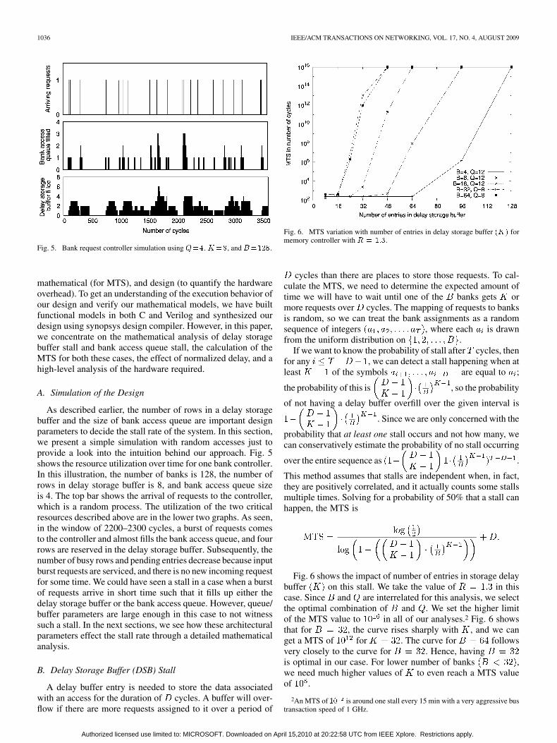
Fig. 6. MTS variation with number of entries in delay storage buffer ��� formemory controller with � � ���.
cycles than there are places to store those requests. To cal-culate the MTS, we need to determine the expected amount oftime we will have to wait until one of the banks gets ormore requests over cycles. The mapping of requests to banksis random, so we can treat the bank assignments as a randomsequence of integers , where each is drawnfrom the uniform distribution on .
If we want to know the probability of stall after cycles, thenfor any , we can detect a stall happening when atleast of the symbols are equal to ;
the probability of this is , so the probability
of not having a delay buffer overfill over the given interval is
. Since we are only concerned with the
probability that at least one stall occurs and not how many, wecan conservatively estimate the probability of no stall occurring
over the entire sequence as .
This method assumes that stalls are independent when, in fact,they are positively correlated, and it actually counts some stallsmultiple times. Solving for a probability of 50% that a stall canhappen, the MTS is
Fig. 6 shows the impact of number of entries in storage delaybuffer on this stall. We take the value of in thiscase. Since and are interrelated for this analysis, we selectthe optimal combination of and . We set the higher limitof the MTS value to in all of our analyses.2 Fig. 6 showsthat for , the curve rises sharply with , and we canget a MTS of for . The curve for followsvery closely to the curve for . Hence, havingis optimal in our case. For lower number of banks ,we need much higher values of to even reach a MTS valueof .
2An MTS of � is around one stall every 15 min with a very aggressive bustransaction speed of 1 GHz.
Authorized licensed use limited to: MICROSOFT. Downloaded on April 15,2010 at 20:22:58 UTC from IEEE Xplore. Restrictions apply.

AGRAWAL AND SHERWOOD: HIGH-BANDWIDTH NETWORK MEMORY SYSTEM THROUGH VIRTUAL PIPELINES 1037
Fig. 7. Markov model that captures the fail probability of a bank access queuewith � � � and � � �. With probability ���, a new request will arrive at anygiven bank, causing there to be � more cycles worth of work.
C. Bank Access Queue (BAQ) Stall
Performing an analysis similar to that presented inSection V-B will not work for the bank access queue be-cause there is no fixed window of time over which we cananalyze the system combinatorially. There is state involvedbecause the queue may cause a stall or not depending on theamount of work left to be done by the memory bank. To analyzethe stall rate of the bank access queue, we determined that thequeue essentially acts as a probabilistic state machine. Eachstate in this machines corresponds to an amount of work leftfor the queue to perform (the number of cycles left until thequeue would be empty). The transitions between these statesare probabilistic, based on whether a new request arrives at thebank controller on any given cycle. If there are no requests inthe queue, then we are at a ground state with no work to bedone. If no new request comes on a cycle, then there is onecycle less work for the queue to do. We know this becauseall the accesses are serialized for a given bank, and as long asthere is something in the queue, work is being done toward itscompletion. If a new request comes in, then there is morecycles worth of work to do. Finally, the queue will overflow ifthere is more than worth of work do, as that is the maximumamount that can be stored.
To do the analysis, we need to combine this abstract statemachine with the probabilities that any transition will occur.Each cycle, a new request will come to a given bank controllerwith probability , and the probability that there will be no newrequest is . The probabilistic state machine that we are leftwith is a Markov model. In Fig. 7, we can see the probabilisticmodel stored both as a directed graph and in an adjacency matrixform labeled .
The adjacency matrix form has a very nice property: Givenan initial starting state at cycle zero, stored as the vector , tocalculate the probability of landing in any state at cycle one, wesimply multiply by . In the example given, there is proba-bility P of being in state 2, 1-P of still being in the idle state. Thisprocess can then be repeated, and to get the distribution of statesafter time steps, we simply multiply by times, which is,of course, . Note that the stall state is an absorbing state,
Fig. 8. MTS variation with number of entries in bank access queue ��� for ourcontroller with � � ���.
so the probability of being in that state should tell us the proba-bility of there ever being a bank overflow on any of the cycles.To calculate that probability, we simply need to calculate .
We use this analysis to figure out the impact of bank requestqueue size on MTS. The effect of normalized delay canalso be directly seen as is directly proportional to . If wedecrease/increase the value of , then we have to decrease/in-crease the value of accordingly. For our memory controllerwith a value of , the MTS graph is shown in Fig. 8. Wefind that for and , the curve for MTS is almostthe same. We can clearly see from the figure that a lower numberof banks can only provide a maximum MTS valueof for even larger values of . Hence, an SDRAM with itssmall number of banks cannot achieve a reasonable MTS. How-ever, for and , we see an exponential increase inMTS with the increasing value of . We can get an MTS offor using 32 or 64 banks. If any application does notdemand a high value of MTS but requires a lower value of nor-malized delay, then we can use the system with a lower value of
and with 32/64 banks. We did not calculate the MTS valuesfor because the large matrix size makes our anal-ysis very difficult (the matrix requires more than 2 GB of mainmemory).
D. Overall Stall Rate
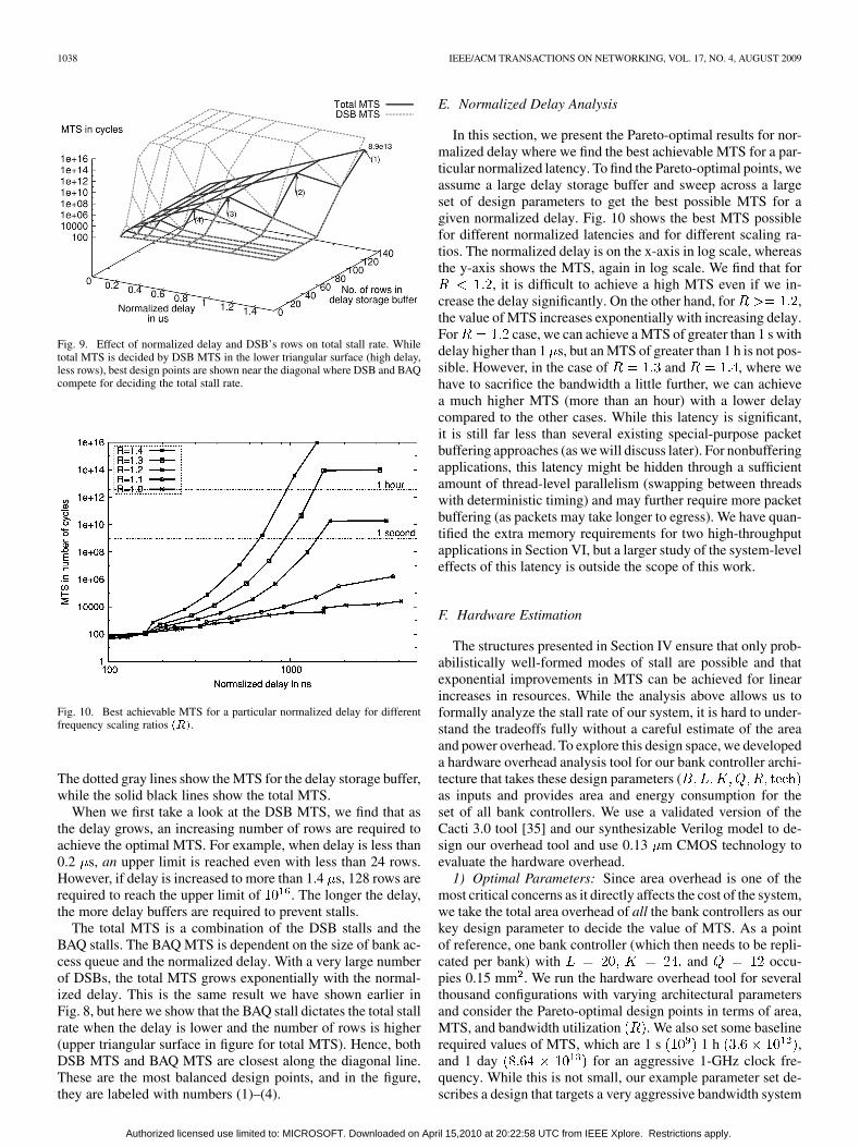
Now that we have analyzed delay storage buffer (DSB)stall and bank access queue (BAQ) stall, we present how totalstall rate is effected based on different parameters. The overallsystem MTS is decided by whether DSB stalls first or BAQstalls first, and hence, it is the minimum of the two. To illustratethe tradeoff between these two stall rates, Fig. 9 shows theMTS as a function of both the normalized delay and the totalnumber of delay buffers. The normalized delay has very crucialrole since it puts pressure on the delay buffers but eases bankaccess queue.
The number of banks is fixed to 32, and the bus scaling ratioto 1.3. We vary the normalized delay up to 1.5 s (shown onx-axis). The normalized delay also represents the size ofbank access queue because it is directly proportional to .On the y-axis, we vary the number of rows in the DSB from 8to 128. The MTS is shown on the z-axis, which is in log scale.
Authorized licensed use limited to: MICROSOFT. Downloaded on April 15,2010 at 20:22:58 UTC from IEEE Xplore. Restrictions apply.
1038 IEEE/ACM TRANSACTIONS ON NETWORKING, VOL. 17, NO. 4, AUGUST 2009
Fig. 9. Effect of normalized delay and DSB’s rows on total stall rate. Whiletotal MTS is decided by DSB MTS in the lower triangular surface (high delay,less rows), best design points are shown near the diagonal where DSB and BAQcompete for deciding the total stall rate.
Fig. 10. Best achievable MTS for a particular normalized delay for differentfrequency scaling ratios ���.
The dotted gray lines show the MTS for the delay storage buffer,while the solid black lines show the total MTS.
When we first take a look at the DSB MTS, we find that asthe delay grows, an increasing number of rows are required toachieve the optimal MTS. For example, when delay is less than0.2 s, an upper limit is reached even with less than 24 rows.However, if delay is increased to more than 1.4 s, 128 rows arerequired to reach the upper limit of . The longer the delay,the more delay buffers are required to prevent stalls.
The total MTS is a combination of the DSB stalls and theBAQ stalls. The BAQ MTS is dependent on the size of bank ac-cess queue and the normalized delay. With a very large numberof DSBs, the total MTS grows exponentially with the normal-ized delay. This is the same result we have shown earlier inFig. 8, but here we show that the BAQ stall dictates the total stallrate when the delay is lower and the number of rows is higher(upper triangular surface in figure for total MTS). Hence, bothDSB MTS and BAQ MTS are closest along the diagonal line.These are the most balanced design points, and in the figure,they are labeled with numbers (1)–(4).
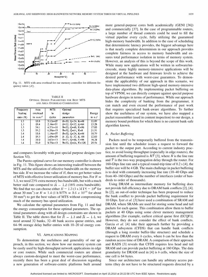
E. Normalized Delay Analysis
In this section, we present the Pareto-optimal results for nor-malized delay where we find the best achievable MTS for a par-ticular normalized latency. To find the Pareto-optimal points, weassume a large delay storage buffer and sweep across a largeset of design parameters to get the best possible MTS for agiven normalized delay. Fig. 10 shows the best MTS possiblefor different normalized latencies and for different scaling ra-tios. The normalized delay is on the x-axis in log scale, whereasthe y-axis shows the MTS, again in log scale. We find that for
, it is difficult to achieve a high MTS even if we in-crease the delay significantly. On the other hand, for ,the value of MTS increases exponentially with increasing delay.For case, we can achieve a MTS of greater than 1 s withdelay higher than 1 s, but an MTS of greater than 1 h is not pos-sible. However, in the case of and , where wehave to sacrifice the bandwidth a little further, we can achievea much higher MTS (more than an hour) with a lower delaycompared to the other cases. While this latency is significant,it is still far less than several existing special-purpose packetbuffering approaches (as we will discuss later). For nonbufferingapplications, this latency might be hidden through a sufficientamount of thread-level parallelism (swapping between threadswith deterministic timing) and may further require more packetbuffering (as packets may take longer to egress). We have quan-tified the extra memory requirements for two high-throughputapplications in Section VI, but a larger study of the system-leveleffects of this latency is outside the scope of this work.
F. Hardware Estimation
The structures presented in Section IV ensure that only prob-abilistically well-formed modes of stall are possible and thatexponential improvements in MTS can be achieved for linearincreases in resources. While the analysis above allows us toformally analyze the stall rate of our system, it is hard to under-stand the tradeoffs fully without a careful estimate of the areaand power overhead. To explore this design space, we developeda hardware overhead analysis tool for our bank controller archi-tecture that takes these design parameters (as inputs and provides area and energy consumption for theset of all bank controllers. We use a validated version of theCacti 3.0 tool [35] and our synthesizable Verilog model to de-sign our overhead tool and use 0.13 m CMOS technology toevaluate the hardware overhead.
1) Optimal Parameters: Since area overhead is one of themost critical concerns as it directly affects the cost of the system,we take the total area overhead of all the bank controllers as ourkey design parameter to decide the value of MTS. As a pointof reference, one bank controller (which then needs to be repli-cated per bank) with and occu-pies 0.15 mm . We run the hardware overhead tool for severalthousand configurations with varying architectural parametersand consider the Pareto-optimal design points in terms of area,MTS, and bandwidth utilization . We also set some baselinerequired values of MTS, which are 1 s 1 h ,and 1 day for an aggressive 1-GHz clock fre-quency. While this is not small, our example parameter set de-scribes a design that targets a very aggressive bandwidth system
Authorized licensed use limited to: MICROSOFT. Downloaded on April 15,2010 at 20:22:58 UTC from IEEE Xplore. Restrictions apply.
AGRAWAL AND SHERWOOD: HIGH-BANDWIDTH NETWORK MEMORY SYSTEM THROUGH VIRTUAL PIPELINES 1039
Fig. 11. MTS with area overhead for our memory controller for different fre-quency ratios ���.
TABLE IIOPTIMAL DESIGN PARAMETERS FOR BEST MTS
AND AREA OVERHEAD COMBINATION
and compares favorably with past special purpose designs (seeSection VI).
The Pareto-optimal curve for our memory controller is shownin Fig. 11. This figure shows an interesting tradeoff between theMTS and the utilization of effective bandwidth on the memorybus side. If we increase the value of , then we get better valuesof MTS with effective lower utilization of memory bus. For
, we need 23% extra memory bus bandwidth, but with a muchbetter stall rate compared to (16% extra bandwidth).We find that we can choose either (1 s forabout 30 mm ) or (1 h for about30 mm ) to get the best values of MTS without compromisingmuch of the memory bus speed utilization.
We calculate the optimal parameters from Fig. 11 and findthe energy consumption for these optimal parameters. The op-timal parameters along with all design constraints are shown inTable II. The table shows that for and , weneed around 32 banks, 32–48 bank access queue entries, and64–96 storage delay buffer entries with 10–20 nJ energy con-sumption.
VI. APPLICATIONS MAPPING
To demonstrate the usefulness and generality of our ap-proach, in this section, we show how our memory system canbe easily used by high-throughput network applications in edgeor core routers. While such commercial routers are almostalways custom-designed to meet the worst-case performance,recently there has been a great deal of discussion regardinga new generation of software-centric platforms built around
more general-purpose cores both academically (GENI [36])and commercially [37]. In the case of programmable routers,a large number of thread contexts could be used to fill thevirtual pipeline every cycle, fully utilizing the guaranteedhigh-memory bandwidth. In addition to the ease of schedulingthat deterministic latency provides, the biggest advantage hereis that nearly complete determinism in our approach providescomplete fairness in access to memory bandwidth and en-sures total performance isolation in terms of memory system.However, an analysis of this is beyond the scope of this work.While many new applications will be written in software/mi-crocode, many highly memory-intensive applications will bedesigned at the hardware and firmware levels to achieve thedesired performance with worst-case guarantees. To demon-strate the applicability of our approach in this scenario, wehave implemented two different high-speed memory-intensivedata-plane algorithms. By implementing packet buffering ontop of VPNM, we can directly compare against special purposehardware designs in terms of performance. While our approachhides the complexity of banking from the programmer, itcan match and even exceed the performance of past workthat requires specialized bank-aware algorithms. To furthershow the usefulness of our system, we have also mapped apacket reassembler (used in content inspection) to our design, amemory bound problem for which there is no current bank-safealgorithm known.
A. Packet Buffering
Packets need to be temporarily buffered from the transmis-sion line until the scheduler issues a request to forward thepacket to the output port. According to current industry prac-tice, to avoid losing throughput (especially in edge routers), theamount of buffering required is [3], where is the line rateand is the two-way propagation delay through the router. For160-Gbps line rate and a typical round-trip time of 0.2 s [4], thebuffer size will be 4 GB. The main challenge in packet bufferingis to deal with constantly increasing line rate (10–40 Gbps andfrom 40–160 Gbps) and the number of interfaces (order of hun-dreds to order of thousands).
Using DRAM as intermediate memory for buffering doesnot provide full efficiency due to DRAM bank conflicts [2], [4].In [2], an out-of-order technique has been proposed to reducethe bank conflict to provide packet buffering requirement for10 Gbps. Iyer et al. [3] have used a combination of SRAM andDRAM, where SRAMs are used for storing some head and tailpackets for each queue. This combination allow them to bufferpackets at 40 Gbps using some clever memory managementalgorithms [for example, earliest critical queue first (ECQF)].However, they do not consider the effect of bank conflicts.Garcia et al. [4] take their approach further by providing aDRAM subsystem (CFDS) that can handle bank conflicts(through a long reorder buffer-like structure) and schedule arequest to DRAM every cycles, where can be less than therandom access time of DRAM. A comparison of their approachand RADS [3] reveals that CFDS requires less head and tailSRAM and can provide packet buffering at 160 Gbps. The datagranularity for DRAM used in [4] is cells, where the size ofone cell is 64 bytes.
Since our architecture can handle any arbitrary access pat-terns (they do not have to be structured requests directed by a
Authorized licensed use limited to: MICROSOFT. Downloaded on April 15,2010 at 20:22:58 UTC from IEEE Xplore. Restrictions apply.

1040 IEEE/ACM TRANSACTIONS ON NETWORKING, VOL. 17, NO. 4, AUGUST 2009
TABLE IIICOMPARISON OF PACKET BUFFERING SCHEMES WITH
OUR GENERALIZED ARCHITECTURE
queue management algorithm), the packet buffering will just bea special case of our system to provide one write access and oneread access. Instead of keeping large head and tail SRAMs tostore packets, we just need to store the head and tail pointers ofeach queue in SRAM. On a read from a particular queue, thehead pointer will be incremented by the packet size, whereas awrite to a particular queue will increment the tail pointer by thepacket size. Our universal hash hardware unit randomizes theaddress from these pointers uniformly across different banks. Inour approach, a request can be issued per cycle, whereas in [4],a request can be issued every cycle. Their architecture is verydifficult to design for as they have also said in their paper,“The implementation of RR scheduling logic for OC-3072 and
is certainly of difficult viability.”As we just need to store the head and tail pointers for each
queue (rather than actual entries in the queue), we can providesupport for a large number of queues (up to 4096 with an SRAMsize of 32 KB—which can be further increased to support evenmore queues). We use the same data granularity used in [4] andcompare our results to [2], RADS [3], and CFDS [4] by takinginto account the throughput, area overhead, normalized delay,and maximum number of supported interfaces. The compar-ison results are provided in Table III for 0.13 m technology.Table III shows that our scheme and CFDS scheme [4] can pro-vide data throughput of 160 Gbps because memory requests canbe scheduled every cycle in our case and every cycles in CFDSscheme. However, our scheme requires about 35% less area, in-troduces 10 times less latency, and can support about five timesthe number of interfaces compared to the CFDS scheme.
B. Packet Reassembly
In an intrusion detection/prevention processing node, the con-tent inspection techniques scan each incoming packet for anymalicious content. Since most of these techniques examine eachpacket irrespective of the ordering/sequence of packets, they areless effective for intrusion detection because a clever attackercan craft out-of-sequence TCP packets such that the worm/virussignature is intentionally divided on the boundary of two re-ordered packets. By doing TCP packet reassembly as a prepro-cessing step, we can ensure that packets are always scanned inorder. In essence, packet reassembly provides a strong front-endto effective content inspection.
While Dharmapurikar et al. [38] have proposed a packetreassembly mechanism that is robust even in the presenceof adversaries, unlike the state-of-the-art in packet bufferingtechniques, their algorithm does not consider the presence ofmemory banks (and, thus, the bounds on performance are nottight). Of course, algorithm designers would rather deal with
network problems than mapping their data structures to banksby hand. VPNM provides exactly that ability, and we havemapped their technique [38] to a virtually pipelined memorysystem. Using the same data granularity for DRAM as in [4]and processing 64 bytes or less each cycle, we find the need toperform one DRAM read access for accessing the connectionrecord, one DRAM access for accessing the correspondinghole-buffer data structure, one DRAM access to update thisdata structure, one DRAM access to write the packet, andone DRAM access to finally read the packet in the future.Hence, for each 64-byte packet chunk, five DRAM accessesare required. Since our memory system can process requestsevery cycle, with a 400-MHz RDRAM [28], we can get aneffective throughput of MHz bytes/s Gbps,which is more than enough to feed the current generation ofcontent inspection engines. We do require some amount ofextra storage space compared to [38] since we need to storeeach packet in FIFO for the duration of three DRAM accesses
, which requires 72 kB of SRAM.
VII. CONCLUSION
Network systems are increasingly asked to perform a va-riety of memory-intensive tasks at very high throughput. Inorder to reliably service traffic with guarantees on throughput,even under worst-case conditions, specialized techniquesare required to handle the variations in latency caused bymemory banking. Certain algorithms can be carefully mappedto memory banks in a way that ensures worst-case performancegoals are met, but this is not always possible and requires carefulplanning at the algorithm, system, and hardware levels. Instead,we present a general-purpose technique for separating these twoconcerns, virtually pipelined network memory, and show that,with provably high confidence, it can simultaneously solve theissues of bank conflicts and bus scheduling for throughput-ori-ented applications. To achieve this deep virtual pipeline, wehad to solve the challenges of multiple conflicting requests,reordering of requests, repeated requests, and timing analysis ofthe system. We have performed rigorous mathematical analysisto show that there is on order of one stall in every memoryaccesses. Furthermore, we have provided a detailed simulation,created a synthesizable version to validate implementability,and estimated hardware overheads to better understand thetradeoffs. To demonstrate the performance and generality ofour virtually pipelined network memory, we have consideredthe problem of packet buffering and packet reassembly. Forpacket buffering application, we find that our scheme requiresabout 35% less area and about 10 times less latency and cansupport about five times more number of interfaces compared tothe best existing scheme for OC-3072 line rate. While we havepresented the packet buffering and reassembly implementationusing our architecture, there is a potential for mapping otherdata-plane algorithms into DRAM, including packet classi-fication, packet inspection, application-oriented networking,software-centric programmable routers, and interesting futuredirections to look at even a broader class of irregular streamingapplications.
REFERENCES
[1] B. Agrawal and T. Sherwood, “Virtually pipelined network memory,”in Proc. 39th Annu. IEEE/ACM Int. Symp. Microarchit. (MICRO 39),2006, pp. 197–207.
Authorized licensed use limited to: MICROSOFT. Downloaded on April 15,2010 at 20:22:58 UTC from IEEE Xplore. Restrictions apply.

AGRAWAL AND SHERWOOD: HIGH-BANDWIDTH NETWORK MEMORY SYSTEM THROUGH VIRTUAL PIPELINES 1041
[2] A. Nikologiannis and M. Katevenis, “Efficient per-flow queueing inDRAM at OC-192 line rate using out-of-order execution techniques,”in Proc. IEEE Int. Conf. Commun. (ICC’2001), Helsinki, Finland, Jun.2001, pp. 2048–2052.
[3] S. Iyer, R. R. Kompella, and N. McKeown, “Designing packet buffersfor router linecards,” Stanford Univ., Tech. Rep. TR02-HPNG-031001,Nov. 2002.
[4] J. Garcia, J. Corbal, L. Cerda, and M. Valero, “Design and implemen-tation of high-performance memory systems for future packet buffers,”in Proc. 36th Annu. IEEE/ACM Int. Symp. Microarchit. (MICRO 36),2003, pp. 373–386.
[5] T. Sherwood, G. Varghese, and B. Calder, “A pipelined memory archi-tecture for high throughput network processors,” in Proc. 30th Annu.Int. Symp. Comput. Archit. (ISCA’03), 2003, pp. 288–299.
[6] J. Hasan, S. Chandra, and T. N. Vijaykumar, “Efficient use of memorybandwidth to improve network processor throughput,” in Proc. 30thAnnu. Int. Symp. Comput. Archit. (ISCA’03), 2003, pp. 300–313.
[7] W. F. Lin, S. K. Reinhardt, and D. Burger, “Reducing DRAM latencieswith an integrated memory hierarchy design,” in Proc. 7th Int. Symp.High-Perform. Comput. Archit. (HPCA’01), 2001, pp. 301–312.
[8] S. Rixner, “Memory controller optimizations for web servers,” in Proc.37th Annu. IEEE/ACM Int. Symp. Microarchit. (MICRO 37), 2004, pp.355–366.
[9] Z. Zhu, Z. Zhang, and X. Zhang, “Fine-grain priority scheduling onmulti-channel memory systems,” in Proc. 8th Int. Symp. High-Perform.Comput. Archit. (HPCA’02), 2002, pp. 107–116.
[10] J. Shao and B. T. Davis, “A burst scheduling access reorderingmechanism,” in Proc. 13th Int. Symp. High-Perform. Comput. Archit.(HPCA’07), 2007, pp. 285–294.
[11] B. K. Mathew, S. A. McKee, J. B. Carter, and A. Davis, “Design ofa parallel vector access unit for SDRAM memory systems,” in Proc.6th Int. Symp. High-Perform. Comput. Archit. (HPCA’00), 2000, pp.39–48.
[12] S. I. Hong, S. A. McKee, M. H. Salinas, R. H. Klenke, J. H. Aylor,and W. A. Wulf, “Access order and effective bandwidth for streamson a direct Rambus memory,” in Proc. 5th Int. Symp. High Perform.Comput. Archit. (HPCA’99), 1999, pp. 80–89.
[13] S. Rixner, W. J. Dally, U. J. Kapasi, P. Mattson, and J. D. Owens,“Memory access scheduling,” in Proc. 27th Annu. Int. Symp. Comput.Archit. (ISCA’00), 2000, pp. 128–138.
[14] R. Espasa, M. Valero, and J. E. Smith, “Out-of-order vector architec-tures,” in Proc. 30th Annu. IEEE/ACM Int. Symp. Microarchit. (MICRO30), 1997, pp. 160–170.
[15] B. R. Rau, “Pseudo-randomly interleaved memory,” in Proc. 18thAnnu. Int. Symp. Comput. Archit. (ISCA’91), 1991, pp. 74–83.
[16] T. Lang, M. Valero, M. Peiron, and E. Ayguade, “Conflict-free accessfor streams in multimodule memories,” IEEE Trans. Comput., vol. 44,no. 5, pp. 634–646, May 1995.
[17] J. Corbal, R. Espasa, and M. Valero, “Command vector memory sys-tems: High performance at low cost,” in Proc. 1998 Int. Conf. ParallelArchit. Compilation Tech. (PACT’98), 1998, pp. 68–79.
[18] F. Chung, R. Graham, and G. Varghese, “Parallelism versus memoryallocation in pipelined router forwarding engines,” in Proc. SPAA, P.B. Gibbons and M. Adler, Eds., 2004, pp. 103–111.
[19] G. A. Bouchard, M. Calle, and R. Ramaswami, “Dynamic random ac-cess memory system with bank conflict avoidance feature,” U.S. Patent6 944 731, Sep. 2005.
[20] G. Shrimali and N. McKeown, “Building packet buffers with inter-leaved memories,” in Proc. Workshop High Perform. Switching andRouting, Hong Kong, May 2005, pp. 1–5.
[21] S. Kumar, P. Crowley, and J. Turner, “Design of randomized multi-channel packet storage for high performance routers,” in Proc. 13thAnnu. Symp. High Perform. Interconnects (Hot Interconnects), PaloAlto, CA, Aug. 2005, pp. 100–106.
[22] F. Baboescu, D. M. Tullsen, G. Rosu, and S. Singh, “A tree based routersearch engine architecture with single port memories,” in Proc. 32ndAnnu. Int. Symp. Comput. Archit. (ISCA’05), 2005, pp. 123–133.
[23] J. Hasan, V. Jakkula, S. Cadambi, and S. Chakradhar, “Chisel: Astorage-efficient, collision-free hash-based packet processing archi-tecture,” in Proc. 33rd Annu. Int. Symp. Comput. Archit. (ISCA 33),Boston, MA, Jun. 2006, pp. 203–215.
[24] R. Crisp, “Direct Rambus technology: The new main memory stan-dard,” IEEE Micro, vol. 17, no. 6, pp. 18–28, Nov./Dec. 1997.
[25] M. Gries, “A survey of synchronous RAM architectures,” ComputerEng. and Networks Lab. (TIK), ETH Zurich, Switzerland, Tech. Rep.71, Apr. 1999.
[26] B. Davis, B. L. Jacob, and T. N. Mudge, “The new DRAM interfaces:SDRAM, RDRAM and variants,” in Proc. 3rd Int. Symp. High Perform.Comput. (ISHPC’00), 2000, pp. 26–31.
[27] V. Cuppu, B. Jacob, B. Davis, and T. Mudge, “A performance compar-ison of contemporary DRAM architectures,” in Proc. 26th Annu. Int.Symp. Comput. Archit. (ISCA’99), 1999, pp. 222–233.
[28] RamBus, “RDRAM memory: Leading performance and value overSDRAM and DDR,” 2001.
[29] Samsung, “Samsung RamBus MR18R162GDF0-CM8 512 MB 16 bit800 MHz datasheet,” 2005.
[30] J. Truong, “Evolution of network memory,” Samsung Semiconductor,Inc., Mar. 2005.
[31] T. Kirihata et al., “An 800 MHz embedded dram with a concurrentrefresh mode,” in Proc. IEEE Int. Solid-State Circuits Conf. (ISSCC),Feb. 2004, pp. 15–19.
[32] J. L. Carter and M. N. Wegman, “Universal classes of hash functions,”J.Comput. Syst. Sci., vol. 18, pp. 143–154, 1979.
[33] E. Jaulmes, A. Joux, and F. Valette, “On the security of randomizedCBC-MAC beyond the birthday paradox limit: A new construction,”in Proc. Revised Papers 9th Int. Workshop. Fast Softw. Encryption(FSE’02), 2002, pp. 237–251.
[34] “Internet core router test: Looking at latency,” 2001[Online]. Available: http://www.lightreading.com/docu-ment.asp?doc_id=4009&page_number=7
[35] P. Shivakumar and N. P. Jouppi, “Cacti 3.0: An integrated cache timing,power and area model,” Western Research Lab (WRL) Res. Rep., Tech.Rep, 2001/2.
[36] J. Turner, “A proposed architecture for the Geni backbone platform,”Mar. 2006.
[37] W. Eatherton, “The push of network processing to the top of thepyramid,” 2005, ANCS’05 Keynote.
[38] S. Dharmapurikar and V. Paxson, “Robust TCP reassembly in the pres-ence of adversaries,” in Proc. 14th USENIX Security Symp., Baltimore,MD, Aug. 2005, pp. 65–80.
Banit Agrawal received the B.Tech. degree in in-strumentation engineering from the Indian Instituteof Technology, Kharagpur, India, in 2001, the M.S.degree in computer science from the Universityof California, Riverside, in 2004, and the Ph.D.degree in computer science from the University ofCalifornia, Santa Barbara, in 2008.
His research interests include memory designand modeling for high-performance networking,3-dimensional ICs, dataflow analysis, security/anal-ysis processors, nanoscale architectures, and
power-aware architectures.Dr. Agrawal was the recipient of a Dean’s Fellowship during 2007–2008, a
best paper award in the International Symposium on Code Generation and Opti-mization (CGO) 2006, a best paper nomination in the 39th Annual IEEE/ACMInternational Symposium on Microarchitecture, 2006, and an IEEE Micro TopPick Award in the Computer Architecture Conference in 2006.
Timothy Sherwood (S’98–M’03) received the B.S.degree from the University of California, Davis, in1998, and the M.S. and Ph.D. degrees from the Uni-versity of California, San Diego, in 2003, where heworked with Prof. B. Calder.
He joined the University of California, Santa Bar-bara (UCSB) in 2003, where he is currently an Assis-tant Professor. His prior work on program phase anal-ysis methods (a technique for reasoning about andpredicting the behavior of programs over time) hasbeen cited over 350 times and is now used by Intel,
Hewlett-Packard (HP), and other industry partners to guide the design of theirlargest microprocessors. His research interests focus on the area of computerarchitecture, specifically in the development of novel high-throughput methodsby which systems can be monitored and analyzed.
Prof. Sherwood was the recipient of a National Science Foundation (NSF)CAREER Award in 2005, and, for the three consecutive years since joiningUCSB, he has received the IEEE Micro Top Pick Award for novel research con-tributions of significance to the computing industry.
Authorized licensed use limited to: MICROSOFT. Downloaded on April 15,2010 at 20:22:58 UTC from IEEE Xplore. Restrictions apply.


![Formalization of Metatheory of the Quipper Quantum ...afelty/dist/jar19MahmoudFelty.pdfQuipper is a functional programming language designed for implementing quantum algo-rithms [17]](https://img.pdfslide.us/doc/110x75/60f57acfcc05c55ddd7f7fb6/formalization-of-metatheory-of-the-quipper-quantum-afeltydistjar19mahmoudfeltypdf.jpg)