Embed Size (px)
Citation preview

IEEE TRANSACTIONS ON VERY LARGE SCALE INTEGRATION (VLSI) SYSTEMS, VOL. 22, NO. 3, MARCH 2014 675
Data Encoding Techniques for Reducing EnergyConsumption in Network-on-Chip
Nima Jafarzadeh, Maurizio Palesi, Member, IEEE, Ahmad Khademzadeh, andAli Afzali-Kusha, Senior Member, IEEE
Abstract— As technology shrinks, the power dissipated by thelinks of a network-on-chip (NoC) starts to compete with thepower dissipated by the other elements of the communicationsubsystem, namely, the routers and the network interfaces (NIs).In this paper, we present a set of data encoding schemes aimedat reducing the power dissipated by the links of an NoC. Theproposed schemes are general and transparent with respect to theunderlying NoC fabric (i.e., their application does not require anymodification of the routers and link architecture). Experimentscarried out on both synthetic and real traffic scenarios show theeffectiveness of the proposed schemes, which allow to save upto 51% of power dissipation and 14% of energy consumptionwithout any significant performance degradation and with lessthan 15% area overhead in the NI.
Index Terms— Coupling switching activity, data encoding,interconnection on chip, low power, network-on-chip (NoC),power analysis.
I. INTRODUCTION
SHIFTING from a silicon technology node to the next oneresults in faster and more power efficient gates but slower
and more power hungry wires [1]. In fact, more than 50%of the total dynamic power is dissipated in interconnects incurrent processors, and this is expected to rise to 65%–80%over the next several years [2]. Global interconnect length doesnot scale with smaller transistors and local wires. Chip sizeremains relatively constant because the chip function continuesto increase and RC delay increases exponentially. At 32/28 nm,for instance, the RC delay in a 1-mm global wire at theminimum pitch is 25× higher than the intrinsic delay of atwo-input NAND fanout of 5 [1].
If the raw computation horsepower seems to be unlimited,thanks to the ability of instancing more and more cores in asingle silicon die, scalability issues, due to the need of makingefficient and reliable communication between the increasing
Manuscript received July 16, 2012; revised February 2, 2013; acceptedFebruary 5, 2013. Date of publication March 28, 2013; date of current versionFebruary 20, 2014.
N. Jafarzadeh is with the Department of Computer Science, Science andResearch Branch, Islamic Azad University, Tehran 14515-775, Iran (e-mail:[email protected]).
M. Palesi is with the Kore University of Enna, Enna 94100, Italy (e-mail:[email protected]).
A. Khademzadeh is with the Iran Telecommunication Research Center,Tehran 16846-13114, Iran (e-mail: [email protected]).
A. Afzali-Kusha is with the School of Electrical and Computer Engineering,College of Engineering, University of Tehran, Tehran 14395, Iran (e-mail:[email protected]).
Color versions of one or more of the figures in this paper are availableonline at http://ieeexplore.ieee.org.
Digital Object Identifier 10.1109/TVLSI.2013.2251020
number of cores, become the real problem [3]. The network-on-chip (NoC) design paradigm [4] is recognized as the mostviable way to tackle with scalability and variability issues thatcharacterize the ultradeep submicronmeter era.
Nowadays, the on-chip communication issues are as relevantas, and in some cases more relevant than, the computation-related issues [4]. In fact, the communication subsystemincreasingly impacts the traditional design objectives, includ-ing cost (i.e., silicon area), performance, power dissipation,energy consumption, reliability, etc. As technology shrinks,an ever more significant fraction of the total power budgetof a complex many-core system-on-chip (SoC) is due to thecommunication subsystem.
In this paper, we focus on techniques aimed at reducingthe power dissipated by the network links. In fact, the powerdissipated by the network links is as relevant as that dissipatedby routers and network interfaces (NIs) and their contributionis expected to increase as technology scales [5]. In particular,we present a set of data encoding schemes operating at flitlevel and on an end-to-end basis, which allows us to mini-mize both the switching activity and the coupling switchingactivity on links of the routing paths traversed by the packets.The proposed encoding schemes, which are transparent withrespect to the router implementation, are presented and dis-cussed at both the algorithmic level and the architecturallevel, and assessed by means of simulation on synthetic andreal traffic scenarios. The analysis takes into account severalaspects and metrics of the design, including silicon area, powerdissipation, and energy consumption. The results show that byusing the proposed encoding schemes up to 51% of powerand up to 14% of energy can be saved without any significantdegradation in performance and with 15% area overhead inthe NI.
The rest of this paper is organized as follows. We brieflydiscuss related works in Section II, while Section III presentsan overview of the proposed data encoding schemes. Theproposed data encoding schemes along with possible hardwareimplementations and their analysis are described in Section IV.In Section V, the results for the hardware overhead, power andenergy savings, and performance reduction of the proposeddata encoding schemes are compared with those of otherapproaches. Finally, this paper is concluded in Section VI.
II. RELATED WORKS AND CONTRIBUTIONS
In the next several years, the availability of chips with 1000cores is foreseen [6]. In these chips, a significant fraction of
1063-8210 © 2013 IEEE. Personal use is permitted, but republication/redistribution requires IEEE permission.See http://www.ieee.org/publications_standards/publications/rights/index.html for more information.

676 IEEE TRANSACTIONS ON VERY LARGE SCALE INTEGRATION (VLSI) SYSTEMS, VOL. 22, NO. 3, MARCH 2014
the total system power budget is dissipated by interconnectionnetworks. Therefore, the design of power-efficient intercon-nection networks has been the focus of many works publishedin the literature dealing with NoC architectures. These worksconcentrate on different components of the interconnectionnetworks such as routers, NIs, and links. Since the focus of thispaper is on reducing the power dissipated by the links, in thissection, we briefly review some of the works in the area of linkpower reduction. These include the techniques that make useof shielding [7], [8], increasing line-to-line spacing [9], [10],and repeater insertion [11]. They all increase the chip area. Thedata encoding scheme is another method that was employedto reduce the link power dissipation. The data encodingtechniques may be classified into two categories. In the firstcategory, encoding techniques concentrate on lowering thepower due to self-switching activity of individual bus lineswhile ignoring the power dissipation owing to their couplingswitching activity. In this category, bus invert (BI) [12] andINC-XOR [13] have been proposed for the case that randomdata patterns are transmitted via these lines. On the otherhand, gray code [14], T0 [15], working-zone encoding [16],and T0-XOR [17] were suggested for the case of correlateddata patterns. Application-specific approaches have also beenproposed [18]–[22].
This category of encoding is not suitable to be applied inthe deep submicronmeter technology nodes where the couplingcapacitance constitutes a major part of the total interconnectcapacitance. This causes the power consumption due to thecoupling switching activity to become a large fraction ofthe total link power consumption, making the aforementionedtechniques, which ignore such contributions, inefficient [23].The works in the second category concentrate on reduc-ing power dissipation through the reduction of the cou-pling switching [10], [22]–[30]. Among these schemes [10],[24]–[28], the switching activity is reduced using many extracontrol lines. For example, the data bus width grows from32 to 55 in [24]. The techniques proposed in [29] and [30]have a smaller number of control lines but the complexity oftheir decoding logic is high. The technique described in [29]is as follows: first, the data are both odd inverted and eveninverted, and then transmission is performed using the kind ofinversion which reduces more the switching activity. In [30],the coupling switching activity is reduced up to 39%. In thispaper, compared to [30], we use a simpler decoder whileachieving a higher activity reduction.
Let us now discuss in more detail the works with whichwe compare our proposed schemes. In [12], the number oftransitions from 0 to 1 for two consecutive flits (the flitthat just traversed and the one which is about to traversethe link) is counted. If the number is larger than half ofthe link width, the inversion will be performed to reducethe number of 0 to 1 transitions when the flit is trans-ferred via the link. This technique is only concerned aboutthe self-switching without worrying the coupling switching.Note that the coupling capacitance in the state-of–the-artsilicon technology is considerably larger (e.g., four times)compared with the self-capacitance, and hence, should be con-sidered in any scheme proposed for the link power reduction.
TABLE I
EFFECT OF ODD INVERSION ON CHANGE OF TRANSITION TYPES
Time Normal Odd Inverted
t − 1
t
Type I Types II, III, and IV
00, 11 00, 11, 01, 10 01, 10 00, 11 00, 11, 01, 10 01, 10
10, 01 01, 10, 00, 11 11, 00 11, 00 00, 11, 01, 10 10, 01
T1* T1** T1*** Type III Type IV Type II
t − 1
t
Type II Type I
01, 10 01, 10
10, 01 11, 00
t − 1
t
Type III Type I
00, 11 00, 11
11, 00 10, 01
t − 1
t
Type IV Type I
00, 11, 01, 10 00, 11, 01, 10
00, 11, 01, 10 01, 10, 00, 11
In addition, the scheme was based on the hop-by-hop tech-nique, and therefore, encoding/decoding is performed in eachnode.
The scheme presented in [26] dealt with reducing thecoupling switching. In this method, a complex encoder countsthe number of Type I (Table I) transitions with a weightingcoefficient of one and the number of Type II transitions withthe weighting coefficient of two. If the number is largerthan half of the link width, the inversion will be performed.In addition to the complex encoder, the technique only workson the patterns whose full inversion leads to the link powerreduction while not considering the patterns whose full inver-sions may lead to higher link power consumption. Therefore,the link power reduction achieved through this technique isnot as large as it could be. This scheme was also based on thehop-by-hop technique.
In another coding technique presented in [25], bunches offour bits are encoded with five bits. The encoded bits wereisolated using shielding wires such that the occurrence ofthe patterns “101” and “010” were prevented. This way, nosimultaneous Type II transitions in two adjacent pair bitsare induced. This technique effectively reduces the couplingswitching activity. Although the technique reduces the powerconsumption considerably, it increases the data transfer time,and, hence, the link energy consumption. This is due to the factthat for each four bits, six bits are transmitted which increasesthe communication traffic. This technique was also based onthe hop-by-hop approach.
A coding technique that reduces the coupling switchingactivity by taking the advantage of end-to-end encoding forwormhole switching has been presented in [23]. It is based onlowering the coupling switching activity by eliminating onlyType II transitions.
In this paper, we present three encoding schemes.In Scheme I, we focus on reducing Type I transitions whilein Scheme II, both Types I and II transitions are taken intoaccount for deciding between half and full invert, dependingthe amount of switching reduction. Finally, in Scheme III,we consider the fact that Type I transitions show differentbehaviors in the case of odd and even inverts and make theinversion which leads to the higher power saving.

JAFARZADEH et al.: DATA ENCODING TECHNIQUES FOR REDUCING ENERGY CONSUMPTION IN NoC 677
III. OVERVIEW OF THE PROPOSAL
The basic idea of the proposed approach is encoding the flitsbefore they are injected into the network with the goal of min-imizing the self-switching activity and the coupling switchingactivity in the links traversed by the flits. In fact, self-switchingactivity and coupling switching activity are responsible for linkpower dissipation. In this paper, we refer to the end-to-endscheme. This end-to-end encoding technique takes advantageof the pipeline nature of the wormhole switching technique [4].Note that since the same sequence of flits passes through allthe links of the routing path, the encoding decision taken atthe NI may provide the same power saving for all the links.For the proposed scheme, an encoder and a decoder block areadded to the NI. Except for the header flit, the encoder encodesthe outgoing flits of the packet such that the power dissipatedby the inter-router point-to-point link is minimized [23].
IV. PROPOSED ENCODING SCHEMES
In this section, we present the proposed encoding schemewhose goal is to reduce power dissipation by minimizing thecoupling transition activities on the links of the interconnectionnetwork. Let us first describe the power model that containsdifferent components of power dissipation of a link. Thedynamic power dissipated by the interconnects and drivers is
P = [T0→1 (Cs + Cl) + TcCc] V 2dd Fck (1)
where T0→1 is the number of 0 → 1 transitions in thebus in two consecutive transmissions, Tc is the number ofcorrelated switching between physically adjacent lines, Cs isthe line to substrate capacitance, Cl is the load capacitance,Cc is the coupling capacitance, Vdd is the supply voltage, andFck is the clock frequency. One can classify four types ofcoupling transitions as described in [26]. A Type I transitionoccurs when one of the lines switches when the other remainsunchanged. In a Type II transition, one line switches from lowto high while the other makes transition from high to low.A Type III transition corresponds to the case where both linesswitch simultaneously. Finally, in a Type IV transition bothlines do not change.
The effective switched capacitance varies from type to type,and hence, the coupling transition activity, Tc, is a weightedsum of different types of coupling transition contributions [26].Therefore
Tc = K1T1 + K2T2 + K3T3 + K4T4 (2)
where Ti is the average number of Type i transition andKi is its corresponding weight. According to [26], we useK1 = 1, K2 = 2, and K3 = K4 = 0. The occurrenceprobability of Types I and II for a random set of data is1/2 and 1/8, respectively. This leads to a higher value forK1T 1 compared with K2T 2 suggesting that minimizing thenumber of Type I transition may lead to a considerable powerreduction. Using (2), one may express (1) as
P = [T0→1 (Cs + Cl) + (T1 + 2T2) Cc] V 2dd Fck. (3)
According to [3], Cl can be neglected
P ∝ T0→1Cs + (T1 + 2T2) Cc. (4)
Here, we calculate the occurrence probability for differenttypes of transitions. Consider that flit (t − 1) and flit (t) referto the previous flit which was transferred via the link andthe flit which is about to pass through the link, respectively.We consider only two adjacent bits of the physical channel.Sixteen different combinations of these four bits could occur(Table I). Note that the first bit is the value of the generic ithline of the link, whereas the second bit represents the valueof its (i + 1)th line. The number of transitions for Types I, II,III, and IV are 8, 2, 2, and 4, respectively. For a randomset of data, each of these sixteen transitions has the sameprobability. Therefore, the occurrence probability for Types I,II, III, and IV are 1/2, 1/8, 1/8, and 1/4, respectively. In therest of this section, we present three data encoding schemesdesigned for reducing the dynamic power dissipation of thenetwork links along with a possible hardware implementationof the decoder.
A. Scheme I
In scheme I, we focus on reducing the numbers of Type Itransitions (by converting them to Types III and IV transi-tions) and Type II transitions (by converting them to Type Itransition). The scheme compares the current data with theprevious one to decide whether odd inversion or no inversionof the current data can lead to the link power reduction.
1) Power Model: If the flit is odd inverted before beingtransmitted, the dynamic power on the link is
P ′ ∝ T ′0→1 + (
K1T ′1 + K2T ′
2 + K3T ′3 + K4T ′
4
)Cc (5)
where T ′0→1, T ′
1, T ′2, T ′
3, and T ′4, are the self-transition activity,
and the coupling transition activity of Types I, II, III, and IV,respectively. Table I reports, for each transition, the relation-ship between the coupling transition activities of the flit whentransmitted as is and when its bits are odd inverted. Data areorganized as follows. The first bit is the value of the genericith line of the link, whereas the second bit represents the valueof its (i + 1)th line. For each partition, the first (second) linerepresents the values at time t − 1 (t).
As Table I shows, if the flit is odd inverted, Types II, III,and IV transitions convert to Type I transitions. In the case ofType I transitions, the inversion leads to one of Types II, III, orType IV transitions. In particular, the transitions indicated asT ∗
1 , T ∗∗1 , and T ∗∗∗
1 in the table convert to Types II, III, and IVtransitions, respectively. Also, we have T ′
0→1 = T0→0(odd) +T0→1(even) where odd/even refers to odd/even lines. Therefore,(5) can be expressed as
P ∝ (T0→0(odd) + T0→1(even)
)Cs
+[K1 (T2+T3+T4)+K2T ∗∗∗1 +K3T ∗
1 +K4T ∗∗1 ]Cc. (6)
Thus, if P > P ′, it is convenient to odd invert the flitbefore transmission to reduce the link power dissipation. Using(4) and (6) and noting that Cc/Cs = 4 [26], we obtain thefollowing odd invert condition
1
4T0→1 + T1 + 2T2 >
1
4
(T0→0(odd) + T0→1(even)
)
+T2 + T3 + T4 + 2T ∗∗∗1 .

678 IEEE TRANSACTIONS ON VERY LARGE SCALE INTEGRATION (VLSI) SYSTEMS, VOL. 22, NO. 3, MARCH 2014
(a)
(b)
Fig. 1. Encoder architecture scheme I. (a) Circuit diagram [27]. (b) Internalview of the encoder block (E).
Also, since T0→1 = T0→1(odd) + T0→1(even), one may write
1
4T0→1(odd) + T1 + 2T2 >
1
4T0→0(odd) + T2 + T3
+T4 + 2T ∗∗∗1 (7)
which is the exact condition to be used to decide whether theodd invert has to be performed. Since the terms T0→1(odd)
and T0→0(odd) are weighted with a factor of 1/4, for linkwidths greater than 16 bits, the misprediction of the invertcondition will not exceed 1.2% on average [23]. Thus, we canapproximate the exact condition as
T1 + 2T2 > T2 + T3 + T4 + 2T ∗∗∗1 . (8)
Of course, the use of the approximated odd invert conditionreduces the effectiveness of the encoding scheme due tothe error induced by the approximation but it simplifies thehardware implementation of encoder. Now, defining
Tx = T3 + T4 + T ∗∗∗1
andTy = T2 + T1 − T ∗∗∗
1 (9)
one can rewrite (8) asTy > Tx . (10)
Assuming the link width of w bits, the total transition betweenadjacent lines is w − 1, and hence
Ty + Tx = w − 1. (11)
Thus, we can write (10) as
Ty >(w − 1)
2. (12)
This presents the condition used to determine whether the oddinversion has to be performed or not.
2) Proposed Encoding Architecture: The proposed encod-ing architecture, which is based on the odd invert conditiondefined by (12), is shown in Fig. 1. We consider a link widthof w bits. If no encoding is used, the body flits are groupedin w bits by the NI and are transmitted via the link. Inour approach, one bit of the link is used for the inversionbit, which indicates if the flit traversing the link has beeninverted or not. More specifically, the NI packs the bodyflits in w − 1 bits [Fig. 1(a)]. The encoding logic E, whichis integrated into the NI, is responsible for deciding if theinversion should take place and performing the inversion ifneeded. The generic block diagram shown in Fig. 1(a) is thesame for all three encoding schemes proposed in this paperand only the block E is different for the schemes. To makethe decision, the previously encoded flit is compared with thecurrent flit being transmitted. This latter, whose w bits are theconcatenation of w − 1 payload bits and a “0” bit, representsthe first input of the encoder, while the previous encoded flitrepresents the second input of the encoder [Fig. 1(b)]. Thew − 1 bits of the incoming (previous encoded) body flit areindicated by Xi (Yi ), i = 0, 1, . . . , w − 2. The wth bit of thepreviously encoded body flit is indicated by inv which showsif it was inverted (inv = 1) or left as it was (inv = 0). In theencoding logic, each Ty block takes the two adjacent bits ofthe input flits (e.g., X1 X2Y1Y2, X2 X3Y2Y3, X3 X4Y3Y4, etc.)and sets its output to “1” if any of the transition types of Ty isdetected. This means that the odd inverting for this pair of bitsleads to the reduction of the link power dissipation (Table I).The Ty block may be implemented using a simple circuit.The second stage of the encoder, which is a majority voterblock, determines if the condition given in (12) is satisfied(a higher number of 1s in the input of the block comparedto 0s). If this condition is satisfied, in the last stage, theinversion is performed on odd bits. The decoder circuit simplyinverts the received flit when the inversion bit is high.
B. Scheme II
In the proposed encoding scheme II, we make use of bothodd (as discussed previously) and full inversion. The fullinversion operation converts Type II transitions to Type IVtransitions. The scheme compares the current data with theprevious one to decide whether the odd, full, or no inversionof the current data can give rise to the link power reduction.
1) Power Model: Let us indicate with P, P ′, and P ′′ thepower dissipated by the link when the flit is transmitted withno inversion, odd inversion, and full inversion, respectively.The odd inversion leads to power reduction when P ′ < P ′′and P ′ < P . The power P ′′ is given by [23]
P ′′ ∝ T1 + 2T ∗∗4 . (13)
Neglecting the self-switching activity, we obtain the conditionP ′ < P ′′ as [see (7) and (13)]
T2 + T3 + T4 + 2T ∗∗∗1 < T1 + 2T ∗∗
4 . (14)
Therefore, using (9) and (11), we can write
2(T2 − T ∗∗
4
)< 2Ty − w + 1. (15)

JAFARZADEH et al.: DATA ENCODING TECHNIQUES FOR REDUCING ENERGY CONSUMPTION IN NoC 679
wlg2
wlg2
wlg2
Fig. 2. Encoder architecture Scheme II.
Based on (12) and (15), the odd inversion condition is obtainedas
2(T2 − T ∗∗
4
)< 2Ty − w + 1 Ty >
(w − 1)
2. (16)
Similarly, the condition for the full inversion is obtained fromP ′′ < P and P ′′ < P ′. The inequality P ′′ < P is satisfiedwhen [23]
T2 > T ∗∗4 . (17)
Therefore, using (15) and (17), the full inversion condition isobtained as
2(T2 − T ∗∗
4
)> 2Ty − w + 1 T2 > T ∗∗
4 . (18)
When none of (16) or (18) is satisfied, no inversion will beperformed.
2) Proposed Encoding Architecture: The operating prin-ciples of this encoder are similar to those of the encoderimplementing Scheme I. The proposed encoding architecture,which is based on the odd invert condition of (16) and the fullinvert condition of (18), is shown in Fig. 2. Here again, thewth bit of the previously and the full invert condition of (18)is shown in Fig. 2. Here again, the wth bit of the previouslyencoded body flit is indicated with inv which defines if it wasodd or full inverted (inv = 1) or left as it was (inv = 0).In this encoder, in addition to the Ty block in the Scheme Iencoder, we have the T2 and T ∗∗
4 blocks which determine ifthe inversion based on the transition types T2 and T ∗∗
4 shouldbe taken place for the link power reduction. The second stageis formed by a set of 1s blocks which count the number of1s in their inputs. The output of these blocks has the width oflog2 w. The output of the top 1s block determines the numberof transitions that odd inverting of pair bits leads to the linkpower reduction. The middle 1s block identifies the numberof transitions whose full inverting of pair bits leads to the linkpower reduction. Finally, the bottom 1s block specifies thenumber of transitions whose full inverting of pair bits leadsto the increased link power. Based on the number of 1s foreach transition type, Module A decides if an odd invert or fullinvert action should be performed for the power reduction.
(a)
(b)
Fig. 3. Decoder architecture Scheme II. (a) Circuit diagram. (b) Internalview of the decoder block (D).
For this module, if (16) or (18) is satisfied, the correspondingoutput signal will become “1.” In case no invert action shouldbe taken place, none of the output is set to “1.” Module Acan be implemented using full-adder and comparator blocks.The circuit diagram of the decoder is shown in Fig. 3. Thew bits of the incoming (previous) body flit are indicated byZi (Ri ), i = 0, 1, . . . , w − 1. The wth bit of the body flit isindicated by inv which shows if it was inverted (inv = 1) orleft as it was (inv = 0). For the decoder, we only need tohave the Ty block to determine which action has been takenplace in the encoder. Based on the outputs of these blocks,the majority voter block checks the validity of the inequalitygiven by (12). If the output is “0” (“1”) and the inv = 1,it means that half (full) inversion of the bits has been per-formed. Using this output and the logical gates, the inversionaction is determined. If two inversion bits were used, theoverhead of the decoder hardware could be substantiallyreduced.
C. Scheme III
In the proposed encoding Scheme III, we add even inversionto Scheme II. The reason is that odd inversion converts someof Type I (T ∗∗∗
1 ) transitions to Type II transitions. As canbe observed from Table II, if the flit is even inverted, thetransitions indicated as T ∗∗
1 /T ∗∗∗1 in the table are converted
to Type IV/Type III transitions. Therefore, the even inversionmay reduce the link power dissipation as well. The schemecompares the current data with the previous one to decidewhether odd, even, full, or no inversion of the current datacan give rise to the link power reduction.
1) Power Model: Let us indicate with P ′, P ′′, and P′′′
thepower dissipated by the link when the flit is transmitted withno inversion, odd inversion, full inversion, and even inversion,respectively. Similar to the analysis given for Scheme I,we can approximate the condition P
′′′< P as
T1 + 2T2 > T2 + T3 + T4 + 2T ∗1 . (19)

680 IEEE TRANSACTIONS ON VERY LARGE SCALE INTEGRATION (VLSI) SYSTEMS, VOL. 22, NO. 3, MARCH 2014
TABLE II
EFFECT OF EVEN INVERSION ON CHANGE OF TRANSITION TYPES
Time Normal Even Inverted
t − 1
t
Type I Types II, III, and IV
01, 10 00, 11, 01, 10 00, 11 01, 10 00, 11, 01, 10 00, 11
00, 11 10, 01, 11, 00 01, 10 10, 01 00, 11, 01, 10 11, 00
T1* T1** T1*** Type II Type IV Type III
t − 1
t
Type II Type I
01, 10 01, 10
10, 01 00, 11
t − 1
t
Type III Type I
00, 11 00, 11
11, 00 01, 10
t − 1
t
Type IV Type I
00, 11, 01, 10 00, 11, 01, 10
00, 11, 01, 10 10, 01, 11, 00
DefiningTe = T2 + T1 − T ∗
1 (20)
we obtain the condition P′′′
< P as
Te >(w − 1)
2. (21)
Similar to the analysis given for scheme II, we can approxi-mate the condition P
′′′< P ′ as
T2 + T3 + T4 + 2T ∗1 < T2 + T3 + T4 + 2T ∗∗∗
1 . (22)
Using (9) and (20), we can rewrite (22) as
Te > Ty . (23)
Also, we obtain the condition P′′′
< P ′′ as [see (13) and (19)]
T2 + T3 + T4 + 2T ∗1 < T1 + 2T ∗∗
4 . (24)
Now, defineTr = T3 + T4 + T ∗
1
andTe = T2 + T1 − T ∗
1 . (25)
Assuming the link width of w bits, the total transition betweenadjacent lines is w − 1, and hence
Te + Tr = w − 1. (26)
Using (26), we can rewrite (24) as
2(T2 − T ∗∗
4
)< 2Te − w + 1. (27)
The even inversion leads to power reduction when P′′′
< P,P
′′′< P ′, and P
′′′< P ′′. Based on (21), (23), and (27), we
obtain
Te >(w − 1)
2, Te >Ty, 2
(T2 − T ∗∗
4
)< 2Te − w+1.
(28)
The full inversion leads to power reduction whenP ′′ < P, P ′′ < P ′, and P ′′ < P
′′′. Therefore, using
(18) and (27), the full inversion condition is obtained as
2(T2 − T ∗∗
4
)> 2Ty − w + 1,
(T2 > T ∗∗
4
)
2(T2 − T ∗∗
4
)> 2Te − w + 1. (29)
wlg2
wlg2
wlg2
wlg2
Fig. 4. Encoder architecture Scheme III.
Similarly, the condition for the odd inversion is obtained fromP ′ < P, P ′ < P ′′, and P ′ < P
′′′. Based on (16) and (23), the
odd inversion condition is satisfied when
2(T2 − T ∗∗
4
)< 2Ty − w + 1, Ty >
(w − 1)
2Te < Ty . (30)
When none of (28), (29), or (30) is satisfied, no inversion willbe performed.
2) Proposed Encoding Architecture: The operating prin-ciples of this encoder are similar to those of the encodersimplementing Schemes I and II. The proposed encoding archi-tecture, which is based on the even invert condition of (28),the full invert condition of (29), and the odd invert conditionof (30), is shown in Fig. 4. The wth bit of the previouslyencoded body flit is indicated by inv which shows if it waseven, odd, or full inverted (inv = 1) or left as it was (inv = 0).The first stage of the encoder determines the transition typeswhile the second stage is formed by a set of 1s blocks whichcount the number of ones in their inputs. In the first stage,we have added the Te blocks which determine if any of thetransition types of T2, T ∗∗
1 , and T ∗∗∗1 is detected for each pair
bits of their inputs. For these transition types, the even invertaction yields link power reduction. Again, we have four Onesblocks to determine the number of detected transitions for eachTy, Te, T2, T ∗∗
4 , blocks. The output of the Ones blocks areinputs for Module C. This module determines if odd, even,full, or no invert action corresponding to the outputs “10,”“01,” “11,” or “00,” respectively, should be performed. Theoutputs “01,” “11,” and “10” show that whether (28), (29),and (30), respectively, are satisfied. In this paper, Module Cwas designed based on the conditions given in (28), (29),and (30). Similar to the procedure used to design the decoderfor scheme II, the decoder for scheme III may be designed.
JAFARZADEH et al.: DATA ENCODING TECHNIQUES FOR REDUCING ENERGY CONSUMPTION IN NoC 681
0%
5%
10%
15%H32
H16 H8
H4
HF32
HF16
HF8
HF4
OEF32
OEF16
OEF8
OEF4
SCS32
SCS16
SCS8
SCS4
SC32
SC16 SC8
SC4
BI32
BI16 BI8
BI4
CDBI32
CDBI16
CDBI8
CDBI4
FPC
% Area Increase % Power Increase
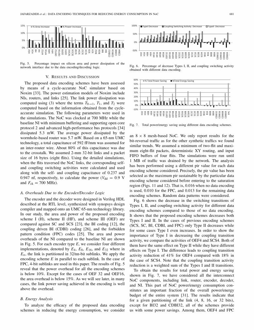
Fig. 5. Percentage impact on silicon area and power dissipation of thenetwork interface due to the data encoding/decoding logic.
V. RESULTS AND DISCUSSION
The proposed data encoding schemes have been assessedby means of a cycle-accurate NoC simulator based onNoxim [33]. The power estimation models of Noxim includeNIs, routers, and links [25]. The link power dissipation wascomputed using (3) where the terms T0→1, T1, and T2 werecomputed based on the information obtained from the cycle-accurate simulation. The following parameters were used inthe simulations. The NoC was clocked at 700 MHz while thebaseline NI with minimum buffering and supporting open coreprotocol 2 and advanced high-performance bus protocols [34]dissipated 5.3 mW. The average power dissipated by thewormhole-based router was 5.7 mW. Based on a 65-nm UMCtechnology, a total capacitance of 592 fF/mm was assumed foran inter-router wire. About 80% of this capacitance was dueto the crosstalk. We assumed 2-mm 32-bit links and a packetsize of 16 bytes (eight flits). Using the detailed simulations,when the flits traversed the NoC links, the corresponding self-and coupling switching activities were calculated and usedalong with the self- and coupling capacitance of 0.237 and0.947 nf, respectively, to calculate the power (Vdd = 0.9 Vand Fck = 700 MHz).
A. Overheads Due to the Encoder/Decoder Logic
The encoder and the decoder were designed in Verilog HDLdescribed at the RTL level, synthesized with synopsys designcompiler and mapped onto an UMC 65-nm technology library.In our study, the area and power of the proposed encodingscheme I (H), scheme II (HF), and scheme III (OEF) arecompared against SC and SCS [23], the BI coding [12], thecoupling driven BI (CDBI) coding [26], and the forbiddenpattern condition (FPC) codes [25]. The area and poweroverheads of the NI compared to the baseline NI are shownin Fig. 5. For each encoder type E, we consider four differentimplementations, denoted by E4, E8, E16, and E32 where inEn , the link is partitioned in 32/nn-bit sublinks. We apply theencoding scheme E in parallel to each sublink. In the case ofFPC, 4-bit sublinks are used in this paper. The results of Fig. 5reveal that the power overhead for all the encoding schemesis below 10%. Except for the cases of OEF 32 and OEF16,the area overhead is below 15%. As we will see later, in manycases, the link power saving achieved in the encoding is wellabove the overhead.
B. Energy Analysis
To analyze the efficacy of the proposed data encodingschemes in reducing the energy consumption, we consider
-50%
0%
50%
100%
H32
H16
H08
H04
HF32
HF16
HF08
HF04
OEF32
OEF16
OEF08
OEF04
SCS32
SCS16
SCS08
SCS04
SC32
SC16
SC08
SC04
BI32 B16
BI08
BI04
CDBI32
CDBI16
CDBI08
CDBI04 FPC
TypeI Decrease Coupling Switching Ac�vity Decrease TypeII Decrease
Fig. 6. Percentage of decrease Types I, II, and coupling switching activityobtained with different data encoding.
-10%
0%
10%
20%
30%
40%
50%
60%
H32
H16
H08
H04
HF32
HF16
HF08
HF04
OEF32
OEF16
OEF08
OEF04
SCS32
SCS16
SCS08
SCS04
SC32
SC16
SC08
SC04
BI32 B16
BI08
BI04
CDBI32
CDBI16
CDBI08
CDBI04 FPC
% Total Power Saving %Total Energy Saving
Fig. 7. Total power/energy saving using different data encoding schemes.
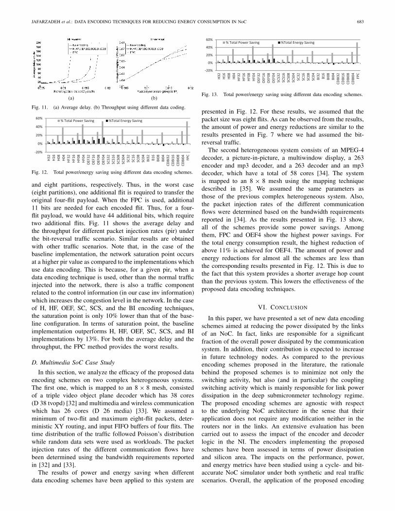
an 8 × 8 mesh-based NoC. We only report results for thebit-reversal traffic as for the other synthetic traffics we foundsimilar trends. We assumed a minimum of two-flit and maxi-mum eight-flit packets, deterministic XY routing, and inputFIFO buffers of four flits. The simulations were run until1 MB of traffic was drained by the network. The analysishas been performed using a different pir value for each dataencoding scheme considered. Precisely, the pir value has beenselected as the maximum pir sustainable by the particular dataencoding scheme considered before entering to the saturationregion (Figs. 11 and 12). That is, 0.016 when no data encodingis used, 0.010 for the FPC, and 0.013 for the remaining dataencoding schemes. Random data patterns were considered.
Fig. 6 shows the decrease in the switching transitions ofTypes I, II, and coupling switching activity for different dataencoding schemes compared to those of no data encoding.It shows that the proposed encoding schemes decreases bothTypes I and II. In the cases of previous encoding schemes(SCS, SC, BI, CDBI, and FPC) only Type II decreases whilefor some cases Type I even increases. In order to show theimportance of Type I in decreasing the coupling transitionactivity, we compare the activities of OEF4 and SCS4. Both ofthem have the same effect on Type II while they have differenteffects on Type I. The difference leads to coupling transitionactivity reduction of 41% for OEF4 compared with 18% inthe case of SCS4. Note that the coupling transition activityreduction is a weighted sum of the Types I and II transitions.
To obtain the results for total power and energy savingshown in Fig. 7, we have considered all the interconnectNoC components, including link, router, encoder, decoder,and NI. This part of NoC power/energy consumption con-stitutes an important fraction of the overall power/energybudget of the entire system [31]. The results indicate thatfor a given partitioning of the link (4, 8, 16, or 32 bits),except for BI32 and CDBI32, all of the schemes provideus with some power savings. Among them, OEF4 and FPC

682 IEEE TRANSACTIONS ON VERY LARGE SCALE INTEGRATION (VLSI) SYSTEMS, VOL. 22, NO. 3, MARCH 2014
-20%
30%
80%
PDFVideoMusicTextPicture
Fig. 8. Total power saving using different data encoding schemes for several data streams.
-30%-20%-10%0%10%20%30%
Video
Music
Text
Picture
Fig. 9. Total energy saving using different data encoding schemes for several data streams.
show the highest power savings. This shows that our proposedschemes (along with the FPC technique) provide more powerreductions when compared with other schemes. In the case ofOEF4, we achieve the highest energy reduction of about 14%.All the proposed techniques provide some energy reductions.Among the schemes, BI and CDBI increase the total energyconsumption. Interestingly, while the power reduction of FPCwas impressive, its energy reduction is not noteworthy. This isdue to the fact that this technique makes use of more than onecontrol bit for coding. Since the bandwidth of the data transferis fixed, having a higher number of control bits leads to alower transfer rate of the actual data, increasing the numberof flits, traffic, and the transfer time. Therefore, the total energyconsumption increases for this scheme.
The power (energy) savings obtained when different datasets including PDF, video, music, text, and picture are usedas the workloads are given in Fig. 8 (Fig. 9). As can beobserved, when the partitioning is based on 4-bit width, all thethree proposed schemes show energy savings for all the datastreams considered in this paper. Also, in the case of OEF4, thesaving is the largest among all the encoding schemes. For thisencoding scheme, the maximum of energy and power morethan 20% and 60%, respectively, was achieved for the pictureworkload.
Finally, it should be pointed out, in general, that the efficacyof any encoding schemes depends on workload data patternswhich are transmitted via the bus. In the cases of the encodingtechniques proposed in this paper, the switching activitiesof two consequent flits of the actual data affect the amountof savings. These activities may vary from one applicationto another. Higher (lower) activities provide more (fewer)opportunities for the power saving by the proposed encodingschemes. Specifically, if an application is dominated by integercomputation, there could be cases that the MSB bits are notalways toggled. This is due to the fact that the range ofnumbers may be limited, and hence, the sign bits may remainunchanged. Of course, this also depends on the representationof the signed numbers. For these applications, the proposedencoding schemes may provide lower power/energy savings.In these cases, one may apply the coding technique only to
0%
10%
20%
30%
40%
50%
60%
0% 10% 20% 30% 40% 50% 60%
%T
otal
Pow
er S
avin
g
% completion time increase
H32 H16H08 H04HF32 HF16HF08 HF04OEF32 OEF16OEF08 OEF04SCS32 SCS16SCS08 SCS04SC32 SC16SC08 SC04BI32 B16BI08 BI04
Fig. 10. Increase of the completion time versus increase of power dissipation.
the bits with higher switching activities as has been performedfor low-power memory addressing schemes (e.g., [22]).
C. Power Versus Performance
The tradeoff between the reduction of the average powerdissipation of the communication system with the completiontime (i.e., the amount of the time needed to drain a givenamount of traffic volume) is an important characteristic ofthe system. The percentage increase of completion time isdefined as the percentage increase of the time needed to draina given amount of traffic. In Fig. 10, this characteristic foreach encoding scheme has been plotted. The average powerdissipation improves almost for all encoding schemes thatare considered in this paper. In this figure, the oblique linecorresponds to equal percentages of power reduction andincreased completion time. The points belonging to the lower(upper) region are characterized by a percentage of completiontime increase which is greater (smaller) than the percentageof power dissipation reduction. From this graph, the OEF, HF,and H are the Pareto-optimal encoding schemes (i.e., are abovethe oblique line).
Let us now compare the average delay and the throughputof a baseline configuration (no data encoding) with a setof network configurations, where we use the proposed dataencoding techniques. We assume 32-bit links and packets offour flits (flit size is 32 bits). The schemes H, HF, OEF,SC, SCS, and BI require one, two, four, and eight additionalbits (inv bits) when the link is divided into one, two, four,
JAFARZADEH et al.: DATA ENCODING TECHNIQUES FOR REDUCING ENERGY CONSUMPTION IN NoC 683
(a) (b)
Fig. 11. (a) Average delay. (b) Throughput using different data coding.
-20%
0%
20%
40%
60%
H32
H16
H08
H04
HF32
HF16
HF08
HF04
OEF32
OEF16
OEF08
OEF04
SCS32
SCS16
SCS08
SCS04
SC32
SC16
SC08
SC04
BI32 B16
BI08
BI04
CDBI32
CDBI16
CDBI08
CDBI04 FPC
% Total Power Saving %Total Energy Saving
Fig. 12. Total power/energy saving using different data encoding schemes.
and eight partitions, respectively. Thus, in the worst case(eight partitions), one additional flit is required to transfer theoriginal four-flit payload. When the FPC is used, additional11 bits are needed for each encoded flit. Thus, for a four-flit payload, we would have 44 additional bits, which requiretwo additional flits. Fig. 11 shows the average delay andthe throughput for different packet injection rates (pir) underthe bit-reversal traffic scenario. Similar results are obtainedwith other traffic scenarios. Note that, in the case of thebaseline implementation, the network saturation point occursat a higher pir value as compared to the implementations whichuse data encoding. This is because, for a given pir, when adata encoding technique is used, other than the normal trafficinjected into the network, there is also a traffic componentrelated to the control information (in our case inv information)which increases the congestion level in the network. In the caseof H, HF, OEF, SC, SCS, and the BI encoding techniques,the saturation point is only 10% lower than that of the base-line configuration. In terms of saturation point, the baselineimplementation outperforms H, HF, OEF, SC, SCS, and BIimplementations by 13%. For both the average delay and thethroughput, the FPC method provides the worst results.
D. Multimedia SoC Case Study
In this section, we analyze the efficacy of the proposed dataencoding schemes on two complex heterogeneous systems.The first one, which is mapped to an 8 × 8 mesh, consistedof a triple video object plane decoder which has 38 cores(D 38 tvopd) [32] and multimedia and wireless communicationwhich has 26 cores (D 26 media) [33]. We assumed aminimum of two-flit and maximum eight-flit packets, deter-ministic XY routing, and input FIFO buffers of four flits. Thetime distribution of the traffic followed Poisson’s distributionwhile random data sets were used as workloads. The packetinjection rates of the different communication flows havebeen determined using the bandwidth requirements reportedin [32] and [33].
The results of power and energy saving when differentdata encoding schemes have been applied to this system are
-20%
0%
20%
40%
60%
H32
H16
H08
H04
HF32
HF16
HF08
HF04
OEF32
OEF16
OEF08
OEF04
SCS32
SCS16
SCS08
SCS04
SC32
SC16
SC08
SC04
BI32 B16
BI08
BI04
CDBI32
CDBI16
CDBI08
CDBI04 FPC
% Total Power Saving %Total Energy Saving
Fig. 13. Total power/energy saving using different data encoding schemes.
presented in Fig. 12. For these results, we assumed that thepacket size was eight flits. As can be observed from the results,the amount of power and energy reductions are similar to theresults presented in Fig. 7 where we had assumed the bit-reversal traffic.
The second heterogeneous system consists of an MPEG-4decoder, a picture-in-picture, a multiwindow display, a 263encoder and mp3 decoder, and a 263 decoder and an mp3decoder, which have a total of 58 cores [34]. The systemis mapped to an 8 × 8 mesh using the mapping techniquedescribed in [35]. We assumed the same parameters asthose of the previous complex heterogeneous system. Also,the packet injection rates of the different communicationflows were determined based on the bandwidth requirementsreported in [34]. As the results presented in Fig. 13 show,all of the schemes provide some power savings. Amongthem, FPC and OEF4 show the highest power savings. Forthe total energy consumption result, the highest reduction ofabove 11% is achieved for OEF4. The amount of power andenergy reductions for almost all the schemes are less thanthe corresponding results presented in Fig. 12. This is due tothe fact that this system provides a shorter average hop countthan the previous system. This lowers the effectiveness of theproposed data encoding techniques.
VI. CONCLUSION
In this paper, we have presented a set of new data encodingschemes aimed at reducing the power dissipated by the linksof an NoC. In fact, links are responsible for a significantfraction of the overall power dissipated by the communicationsystem. In addition, their contribution is expected to increasein future technology nodes. As compared to the previousencoding schemes proposed in the literature, the rationalebehind the proposed schemes is to minimize not only theswitching activity, but also (and in particular) the couplingswitching activity which is mainly responsible for link powerdissipation in the deep submicronmeter technology regime.The proposed encoding schemes are agnostic with respectto the underlying NoC architecture in the sense that theirapplication does not require any modification neither in therouters nor in the links. An extensive evaluation has beencarried out to assess the impact of the encoder and decoderlogic in the NI. The encoders implementing the proposedschemes have been assessed in terms of power dissipationand silicon area. The impacts on the performance, power,and energy metrics have been studied using a cycle- and bit-accurate NoC simulator under both synthetic and real trafficscenarios. Overall, the application of the proposed encoding

684 IEEE TRANSACTIONS ON VERY LARGE SCALE INTEGRATION (VLSI) SYSTEMS, VOL. 22, NO. 3, MARCH 2014
schemes allows savings up to 51% of power dissipation and14% of energy consumption without any significant perfor-mance degradation and with less than 15% area overhead inthe NI.
REFERENCES
[1] International Technology Roadmap for Semiconductors. (2011) [Online].Available: http://www.itrs.net
[2] M. S. Rahaman and M. H. Chowdhury, “Crosstalk avoidance and error-correction coding for coupled RLC interconnects,” in Proc. IEEE Int.Symp. Circuits Syst., May 2009, pp. 141–144.
[3] W. Wolf, A. A. Jerraya, and G. Martin, “Multiprocessor system-on-chipMPSoC technology,” IEEE Trans. Comput.-Aided Design Integr. CircuitsSyst., vol. 27, no. 10, pp. 1701–1713, Oct. 2008.
[4] L. Benini and G. De Micheli, “Networks on chips: A new SoCparadigm,” Computer, vol. 35, no. 1, pp. 70–78, Jan. 2002.
[5] S. E. Lee and N. Bagherzadeh, “A variable frequency link for a power-aware network-on-chip (NoC),” Integr. VLSI J., vol. 42, no. 4,pp. 479–485, Sep. 2009.
[6] D. Yeh, L. S. Peh, S. Borkar, J. Darringer, A. Agarwal, and W. M. Hwu,“Thousand-core chips roundtable,” IEEE Design Test Comput., vol. 25,no. 3, pp. 272–278, May–Jun. 2008.
[7] A. Vittal and M. Marek-Sadowska, “Crosstalk reduction for VLSI,”IEEE Trans. Comput.-Aided Design Integr. Circuits Syst., vol. 16, no. 3,pp. 290–298, Mar. 1997.
[8] M. Ghoneima, Y. I. Ismail, M. M. Khellah, J. W. Tschanz, and V. De,“Formal derivation of optimal active shielding for low-power on-chipbuses,” IEEE Trans. Comput.-Aided Design Integr. Circuits Syst., vol. 25,no. 5, pp. 821–836, May 2006.
[9] L. Macchiarulo, E. Macii, and M. Poncino, “Wire placement forcrosstalk energy minimization in address buses,” in Proc. Design Autom.Test Eur. Conf. Exhibit., Mar. 2002, pp. 158–162.
[10] R. Ayoub and A. Orailoglu, “A unified transformational approach forreductions in fault vulnerability, power, and crosstalk noise and delayon processor buses,” in Proc. Design Autom. Conf. Asia South Pacific,vol. 2. Jan. 2005, pp. 729–734.
[11] K. Banerjee and A. Mehrotra, “A power-optimal repeater insertionmethodology for global interconnects in nanometer designs,” IEEETrans. Electron Devices, vol. 49, no. 11, pp. 2001–2007, Nov. 2002.
[12] M. R. Stan and W. P. Burleson, “Bus-invert coding for low-powerI/O,” IEEE Trans. Very Large Scale Integr. (VLSI) Syst., vol. 3, no. 1,pp. 49–58, Mar. 1995.
[13] S. Ramprasad, N. R. Shanbhag, and I. N. Hajj, “A coding frameworkfor low-power address and data busses,” IEEE Trans. Very Large ScaleIntegr. (VLSI) Syst., vol. 7, no. 2, pp. 212–221, Jun. 1999.
[14] C. L. Su, C. Y. Tsui, and A. M. Despain, “Saving power in the controlpath of embedded processors,” IEEE Design Test Comput., vol. 11, no. 4,pp. 24–31, Oct.–Dec. 1994.
[15] L. Benini, G. De Micheli, E. Macii, D. Sciuto, and C. Silvano, “Asymp-totic zero-transition activity encoding for address busses in low-powermicroprocessor-based systems,” in Proc. 7th Great Lakes Symp. VLSI,Mar. 1997, pp. 77–82.
[16] E. Musoll, T. Lang, and J. Cortadella, “Working-zone encoding forreducing the energy in microprocessor address buses,” IEEE Trans. VeryLarge Scale Integr. (VLSI) Syst., vol. 6, no. 4, pp. 568–572, Dec. 1998.
[17] W. Fornaciari, M. Polentarutti, D. Sciuto, and C. Silvano, “Poweroptimization of system-level address buses based on software profil-ing,” in Proc. 8th Int. Workshop Hardw. Softw. Codesign, May 2000,pp. 29–33.
[18] L. Benini, G. De Micheli, E. Macii, M. Poncino, and S. Quer, “Poweroptimization of core-based systems by address bus encoding,” IEEETrans. Very Large Scale Integr. (VLSI) Syst., vol. 6, no. 4, pp. 554–562,Dec. 1998.
[19] L. Benini, A. Macii, M. Poncino, and R. Scarsi, “Architectures andsynthesis algorithms for power-efficient bus interfaces,” IEEE Trans.Comput.-Aided Design Integr. Circuits Syst., vol. 19, no. 9, pp. 969–980,Sep. 2000.
[20] G. Ascia, V. Catania, M. Palesi, and A. Parlato, “Switching activityreduction in embedded systems: A genetic bus encoding approach,” IEEProc. Comput. Digit. Tech., vol. 152, no. 6, pp. 756–764, Nov. 2005.
[21] R. Siegmund, C. Kretzschmar, and D. Muller, “Adaptive Partial Bus-invert encoding for power efficient data transfer over wide systembuses,” in Proc. 13th Symp. Integr. Circuits Syst. Design, Sep. 2000,pp. 371–376.
[22] S. Youngsoo, C. Soo-Ik, and C. Kiyoung, “Partial bus-invert coding forpower optimization of application-specific systems,” IEEE Trans. VeryLarge Scale Integr. (VLSI) Syst., vol. 9, no. 2, pp. 377–383, Apr. 2001.
[23] M. Palesi, G. Ascia, F. Fazzino, and V. Catania, “Data encoding schemesin networks on chip,” IEEE Trans. Comput.-Aided Design Integr. CircuitsSyst., vol. 30, no. 5, pp. 774–786, May 2011.
[24] C. G. Lyuh and T. Kim, “Low-power bus encoding with crosstalkdelay elimination,” IEE Proc. Comput. Digit. Tech., vol. 153, no. 2,pp. 93–100, Mar. 2006.
[25] P. P. Pande, H. Zhu, A. Ganguly, and C. Grecu, “Energy reduc-tion through crosstalk avoidance coding in NoC paradigm,” in Proc.9th EUROMICRO Conf. Digit. Syst. Design Archit. Methods Tools,Sep. 2006, pp. 689–695.
[26] K. W. Ki, B. Kwang Hyun, N. Shanbhag, C. L. Liu, and K. M.Sung, “Coupling-driven signal encoding scheme for low-power inter-face design,” in Proc. IEEE/ACM Int. Conf. Comput.-Aided Design,Nov. 2000, pp. 318–321.
[27] L. Rung-Bin, “Inter-wire coupling reduction analysis of bus-invertcoding,” IEEE Trans. Circuits Syst. I, Reg. Papers, vol. 55, no. 7,pp. 1911–1920, Aug. 2008.
[28] Z. Khan, T. Arslan, and A. T. Erdogan, “Low power system on chip busencoding scheme with crosstalk noise reduction capability,” IEE Proc.Comput. Digit. Tech., vol. 153, no. 2, pp. 101–108, Mar. 2006.
[29] Z. Yan, J. Lach, K. Skadron, and M. R. Stan, “Odd/even bus invert withtwo-phase transfer for buses with coupling,” in Proc. Int. Symp. LowPower Electron. Design, 2002, pp. 80–83.
[30] C. P. Fan and C. H. Fang, “Efficient RC low-power bus encodingmethods for crosstalk reduction,” Integr. VLSI J., vol. 44, no. 1,pp. 75–86, Jan. 2011.
[31] S. R. Vangal, J. Howard, G. Ruhl, S. Dighe, H. Wilson, J. Tschanz,W. James, D. Finan, A. P. Singh, T. Jacob, S. Jain, V. Erraguntla,C. Roberts, Y. V. Hoskote, N. Y. Borkar, and S. Y. Borkar, “An 80-tileSub-100-W TeraFLOPS processor in 65-nm CMOS,” IEEE J. Solid-StateCircuits, vol. 43, no. 1, pp. 29–41, Jan. 2008.
[32] S. Murali, C. Seiculescu, L. Benini, and G. De Micheli, “Synthesis ofnetworks on chips for 3D systems on chips,” in Proc. Asia South PacificDesign Autom. Conf., Jan. 2009, pp. 242–247.
[33] C. Seiculescu, S. Murali, L. Benini, and G. De Micheli, “SunFloor 3D:A tool for networks on chip topology synthesis for 3-D systems onchips,” in Proc. IEEE Trans. Comput.-Aided Design Integr. Circuits Syst.,vol. 29, no. 12, pp. 1987–2000, Dec. 2010.
[34] S. Murali and G. De Micheli, “Bandwidth-constrained mapping ofcores onto NoC architectures,” in Proc. Design, Autom. Test Eur. Conf.Exhibit., vol. 2. Feb. 2004, pp. 896–901.
[35] M. Palesi, R. Tornero, J. M. Orduñna, V. Catania, and D. Panno,“Designing robust routing algorithms and mapping cores in networks-on-chip: A multi-objective evolutionary-based approach,” J. Univ. Comput.Sci., vol. 18, no. 7, pp. 937–969, 2012.
Nima Jafarzadeh was born in Marand, Iran, in1982. He received the Master of Computer Archi-tecture degree from the Azad University Scienceand Research Branch, Tehran, Iran, 2009, wherehe is currently pursuing the Ph.D. degree from theDepartment of Computer Engineering.
His current research interests include network-on-chips, low power interconnection, reliable intercon-nection, and analytical modeling.
Maurizio Palesi (M’06) received the M.S. andPh.D. degrees in computer engineering from theUniversità di Catania, Catania, Italy, in 1999 and2003, respectively.
He has been an Assistant Professor with KoreUniversity, Enna, Italy, since 2010.
Dr. Palesi serves as the Technical Program Com-mittee Member for the following IEEE/ACM Inter-national Conferences: RTAS, CODES+ISSS, DATE,NOCS, ESTIMedia, SOCC, VLSI, ISC, and SITIS.He was also the Co-organizer of International Work-
shops on Network-on-Chip Architectures in 2008, 2009, and 2010, respec-tively.

JAFARZADEH et al.: DATA ENCODING TECHNIQUES FOR REDUCING ENERGY CONSUMPTION IN NoC 685
Ahmad Khademzadeh received the B.Sc. degree inapplied physics from Ferdowsi University, Mashhad,Iran, in 1969, and the M.Sc. and Ph.D. degrees indigital communication and information theory anderror control coding from the University of Kent,Kent, U.K.
He is currently the Head of Education and NationalScientific and International Scientific CooperationDepartment, Iran Telecom Research Center (ITRC),Tehran, Iran. He was the Head of Test EngineeringGroup and the Director of Computer and Commu-
nication Department, ITRC. He is also a Lecturer with Tehran Universitiesand is a Committee Member of the Iranian Electrical Engineering ConferencePermanent Committee.
Dr. Khadem-Zadeh was selected as the National Outstanding Researcher ofthe Iran Ministry of Information and Communication Technology.
Ali Afzali-Kusha (SM’06) received the B.Sc.,M.Sc., and Ph.D. degrees in electrical engineeringfrom the Sharif University of Technology, Tehran,Iran, University of Pittsburgh, Pittsburgh, PA, USA,and the University of Michigan, Ann Arbor, MI,USA, in 1988, 1991, and 1994, respectively.
He was a Post-Doctoral Fellow with the Universityof Michigan, from 1994 to 1995. Since 1995, he hasbeen with The University of Tehran, Tehran, wherehe is currently a Professor with the School of Elec-trical and Computer Engineering and the Director of
Low-Power High-Performance Nanosystems Laboratory. Also, on a researchleave from the University of Tehran, Tehran, he has been a Research Fellowwith the University of Toronto, Toronto, ON, Canada, and the University ofWaterloo, Waterloo, ON, Canada, in 1998 and 1999, respectively. His currentresearch interests include low-power high-performance design methodologiesfrom the physical design level to the system level for nanoelectronics era.


![Ultra-low power circuits for power management · power dissipation per unit area increases, which could lead to a violation on the design constraints [1]. Therefore, the power dissipation](https://img.pdfslide.us/doc/110x75/5e08c7205038cb62b4616245/ultra-low-power-circuits-for-power-management-power-dissipation-per-unit-area-increases.jpg)