Embed Size (px)
Citation preview
IEEE TRANSACTIONS ON POWER ELECTRONICS, VOL. 20, NO. 4, JULY 2005 857
Z-Source Inverter for Motor DrivesFang Zheng Peng, Fellow, IEEE, Alan Joseph, Jin Wang, Student Member, IEEE, Miaosen Shen, Student Member, IEEE,
Lihua Chen, Zhiguo Pan, Student Member, IEEE, Eduardo Ortiz-Rivera, Member, IEEE, and Yi Huang
Abstract—This paper presents a Z-source inverter system andcontrol for general-purpose motor drives. The Z-source invertersystem employs a unique LC network in the dc link and a smallcapacitor on the ac side of the diode front end. By controlling theshoot-through duty cycle, the Z-source can produce any desiredoutput ac voltage, even greater than the line voltage. As a result,the new Z-source inverter system provides ride-through capabilityduringvoltage sags, reduces line harmonics, improves power factorand reliability, and extends output voltage range. Analysis, simu-lation, and experimental results will be presented to demonstratethese new features.
Index Terms—Line harmonics, motor drives, voltage sags,Z-source inverter.
I. INTRODUCTION
THE TRADITIONAL general-purpose motor drive (oradjustable speed drive—ASD) system is based on the
voltage-source inverter (V-source inverter), which consists of adiode rectifier front end, dc link capacitor, and inverter bridge,as shown in Fig. 1. In order to improve power factor, eitheran ac inductor or dc inductor is normally used. The dc linkvoltage is roughly equal to 1.35 times the line voltage, andthe V-source inverter is a buck (or step-down) converter thatcan only produce an ac voltage limited by the dc link voltage.Because of this nature, the V-source inverter based ASD systemsuffers the following common limitations and problems.
1) Obtainable output voltage is limited quite below the inputline voltage. Fig. 1 illustrates voltages of a three-phase230-V drive system. The diode rectifier fed by the 230-Vac line produces about 310-V dc on the dc-link, which isroughly 1.35 times the line-to-line input voltage under theassumption of heavy load and continuous “double-hump”input current for large ( 50 kW) drives that typicallyhave an approximately 3% of inductance on the ac or dcside. For light load operation or small drives with no sig-nificant inductance, the line current becomes discontin-uous “double-pulse,” and the dc voltage is closer to 1.41times the line-to-line input voltage (i.e., 325-V dc for a230-V ac input). The inverter can only produce a max-imum 190-V ac in the linear modulation range given the310-V dc under the heavy load operation when the voltageis needed the most. For a 230-V motor, the low obtain-able output voltage significantly limits output power thatis proportional to the square of the voltage. This is a very
Manuscript received April 21, 2004; revised September 17, 2004. Recom-mended by Associate Editor J. H. R. Enslin.
The authors are with the Department of Electrical and Computer Engi-neering, Michigan State University, East Lansing, MI 48824 USA (e-mail:[email protected]; [email protected]).
Digital Object Identifier 10.1109/TPEL.2005.850938
Fig. 1. Traditional variable speed drive system configuration.
Fig. 2. Voltage sag results in dc link voltage drop and shut down.
undesirable situation for many applications because themotor and drive system has to be oversized for a requiredpower.
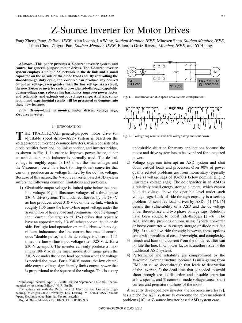
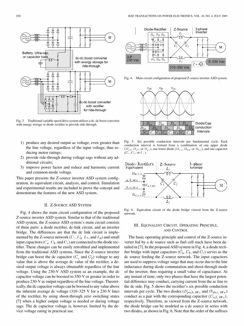
2) Voltage sags can interrupt an ASD system and shutdown critical loads and processes. Over 90% of powerquality related problems are from momentary (typically0.1–2 s) voltage sags of 10–50% below nominal (Fig. 2illustrates voltage sags). The dc capacitor in an ASD isa relatively small energy storage element, which cannothold dc voltage above the operable level under suchvoltage sags. Lack of ride-through capacity is a seriousproblem for sensitive loads driven by ASDs [1]–[6]. [6]details the vulnerability of a ASD and the dc voltageunder three-phase and two phase voltage sags. Solutionshave been sought to boost ride-through [2]–[6]. TheASD industry provides options using flyback converteror boost converter with energy storage or diode rectifier(Fig. 3) to achieve ride-through; however, these optionscome with penalties of cost, size/weight, and complexity.
3) Inrush and harmonic current from the diode rectifier canpollute the line. Low power factor is another issue of thetraditional ASD system.
4) Performance and reliability are compromised by theV-source inverter structure, because 1) miss-gating fromEMI can cause shoot-through that leads to destructionof the inverter, 2) the dead time that is needed to avoidshoot-through creates distortion and unstable operationat low speeds, and 3) common-mode voltage causes shaftcurrent and premature failures of the motor.
A recently developed new inverter, the Z-source inverter [7],has a niche for ASD systems to overcome the aforementionedproblems [10]. A Z-source inverter based ASD system can:
0885-8993/$20.00 © 2005 IEEE
858 IEEE TRANSACTIONS ON POWER ELECTRONICS, VOL. 20, NO. 4, JULY 2005
Fig. 3. Traditional variable speed drive system utilizes a dc–dc boost converterwith energy storage or diode rectifier to provide ride-through.
1) produce any desired output ac voltage, even greater thanthe line voltage, regardless of the input voltage, thus re-ducing motor ratings;
2) provide ride-through during voltage sags without any ad-ditional circuits;
3) improve power factor and reduce and harmonic currentand common-mode voltage.
This paper presents the Z-source inverter ASD system config-uration, its equivalent circuit, analysis, and control. Simulationand experimental results are included to prove the concept anddemonstrate the features of the new ASD system.
II. Z-SOURCE ASD SYSTEM
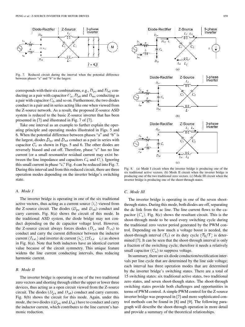
Fig. 4 shows the main circuit configuration of the proposedZ-source inverter ASD system. Similar to that of the traditionalASD system, the Z-source ASD system’s main circuit consistsof three parts: a diode rectifier, dc-link circuit, and an inverterbridge. The differences are that the dc link circuit is imple-mented by the Z-source network ( , and ) and smallinput capacitors ( , and ) are connected to the diode rec-tifier. These changes can be easily retrofitted and implementedfrom the traditional ASD systems. Since the Z-source inverterbridge can boost the dc capacitor ( and ) voltage to anyvalue that is above the average dc value of the rectifier, a de-sired output voltage is always obtainable regardless of the linevoltage. Using the 230-V ASD system as an example, the dccapacitor voltage can be boosted to 350-V or greater in order toproduce 230-V ac output regardless of the line voltage. Theoret-ically, the dc capacitor voltage can be boosted to any value abovethe inherent average dc voltage (310–325 V for a 230-V line)of the rectifier, by using shoot-through zero switching states[7] when a higher output voltage is needed or during voltagesags. The dc capacitor voltage is, however, limited by the de-vice voltage rating in practical use.
Fig. 4. Main circuit configuration of proposed Z-source inverter ASD system.
Fig. 5. Six possible conduction intervals per fundamental cycle. Eachconduction interval is formed from a combination of one upper diode(D ;D , or D ), one lower diode (D ;D , or D ), and one capacitor(C ;C , or C ).
Fig. 6. Equivalent circuit of the diode bridge viewed from the Z-sourcenetwork.
III. EQUIVALENT CIRCUIT, OPERATING PRINCIPLE,AND CONTROL
The basic operating principle and control of the Z-source in-verter fed by a dc source such as fuel cell stack have been de-tailed in [7]. In the proposed ASD system in Fig. 4, a diode recti-fier bridge with input capacitors ( , and ) serves as thedc source feeding the Z-source network. The input capacitorsare used to suppress voltage surge that may occur due to the lineinductance during diode commutation and shoot-through modeof the inverter, thus requiring a small value of capacitance. Atany instant of time, only two phases that have the largest poten-tial difference may conduct, carrying current from the ac line tothe dc side. Fig. 5 shows the rectifier’s six possible conductionintervals per cycle. The two diodes ( or and or )conduct as a pair with the corresponding capacitor or ,respectively. Therefore, as viewed from the Z-source network,the diode bridge can be modeled as a dc source in series withtwo diodes, as shown in Fig. 6. Note that the order of the suffixes
PENG et al.: Z-SOURCE INVERTER FOR MOTOR DRIVES 859
Fig. 7. Reduced circuit during the interval when the potential differencebetween phases “a” and “b” is the largest.
corresponds with their six combinations, e.g., and con-ducting as a pair with capacitor and conducting asa pair with capacitor , and so on. Furthermore, the two diodesconduct in a pair and in series acting like one when viewed fromthe Z-source network. As a result, the proposed Z-source ASDsystem is reduced to the basic Z-source inverter that has beenpresented in [7] and illustrated in Fig. 7 of [7].
Take one interval as an example to further explain the oper-ating principle and operating modes illustrated in Figs. 5 and6. When the potential difference between phases “a” and “b” isthe largest, diodes and conduct as a pair in series withcapacitor as shown in Figs. 5 and 6. The other diodes arereversely biased and cut off. Therefore, phase “c” has no linecurrent (or a small resonant/or residual current may exist be-tween the line impedance and capacitors and ). Ignoringthis small current in phase “c,” Fig. 4 can be reduced into Fig. 7.During this interval and from this reduced circuit, there are threeoperation modes depending on the inverter bridge’s switchingstate.
A. Mode I
The inverter bridge is operating in one of the six traditionalactive vectors, thus acting as a current source viewed fromthe Z-source circuit. The diodes ( and ) conduct andcarry currents. Fig. 8(a) shows the circuit of this mode. Inthe traditional ASD system, the diode bridge may not con-duct depending on the dc capacitor voltage level. However,the Z-source circuit always forces diodes ( and ) toconduct and carry the current difference between the inductorcurrent and inverter dc current as shownin Fig. 8(a). Note that both inductors have an identical currentvalue because of the circuit symmetry. This unique featurewidens the line current conducting intervals, thus reducingharmonic current.
B. Mode II
The inverter bridge is operating in one of the two traditionalzero vectors and shorting through either the upper or lower threedevices, thus acting as a open circuit viewed from the Z-sourcecircuit. The diodes ( and ) conduct and carry currents.Fig. 8(b) shows the circuit for this mode. Again, under thismode, the two diodes (( and ) have to conduct and carrythe inductor current, which contributes to the line current’s har-monic reduction.
(a)
(b)
(c)
Fig. 8. (a) Mode I circuit when the inverter bridge is producing one of thesix traditional active vectors. (b) Mode II circuit when the inverter bridge isproducing one of the two traditional zero vectors. (c) Mode III circuit when theinverter bridge is producing one of the shoot-through states.
C. Mode III
The inverter bridge is operating in one of the seven shoot-through states. During this mode, both diodes are off, separatingthe dc link from the ac line. The line current flows to the ca-pacitor . Fig. 8(c) shows the resultant circuit. This is theshoot-through mode to be used every switching cycle duringthe traditional zero vector period generated by the PWM con-trol. Depending on how much a voltage boost is needed, theshoot-through interval or its duty cycle is deter-mined [7]. It can be seen that the shoot-through interval is onlya fraction of the switching cycle; therefore it needs a relativelysmall capacitor to suppress voltage.
In summary, there are six diode conduction/rectification inter-vals per line cycle that are determined by the line side voltage;each interval has three operation modes that are determinedby the inverter bridge’s switching states. There are a total of15 switching states: six traditional active states, two traditionalzero states, and seven shoot-though states. The shoot-throughswitching states provide both challenges and opportunities interms of PWM control. A simple PWM control for the Z-sourceinverter bridge was proposed in [7] and more sophisticated con-trol methods can be found in [8] and [9]. The following para-graph will describe the shoot-through operation in more detailand provide a summary of the theoretical relationships.
860 IEEE TRANSACTIONS ON POWER ELECTRONICS, VOL. 20, NO. 4, JULY 2005
The operating principle and control of the Z-source inverteritself have been detailed in [7]. The traditional three-phaseV-source inverter has six active states in which the dc voltageis impressed across the load and two zero states, in which theload terminals are shorted through either the lower or upperthree devices, respectively. However, the three-phase Z-sourceinverter bridge has additional zero states when the load termi-nals are shorted through both the upper and lower devices ofany one phase leg (i.e., both devices are gated on), any twophase legs, or all the three phase legs. These shoot-throughzero states are forbidden in the traditional V-source inverter,because it would cause a shoot-through. There are seven dif-ferent shoot-through states: three shoot-through states via anyone phase leg, three shoot-through states from combinationsof any two phase legs, and one shoot-through state by allthe three phase legs. The shoot-through zero states boost dccapacitor voltage while producing no voltage to the load. Itshould be emphasized that both the shoot-through zero statesand the two traditional zero states short the load terminalsand produce zero voltage across the load, thus preserving thesame PWM properties and voltage waveforms to the load. Theonly difference is the shoot-through zero states boost the dccapacitor voltage, whereas the traditional zero states do not.For the proposed ASD system, the three-phase inverter bridgeis controlled the same way as the traditional PWM inverterwithout shoot-through when a desired output voltage is lessthan 190-V ac, which is the maximum voltage obtainable from230-V line using the linear region PWM. The diode rectifierproduces about 310 V across the dc capacitors ( and ).When a higher output voltage is required or when the linevoltage is experiencing sags, the shoot-through zero states areemployed to boost the dc capacitor voltage. The longer time theshoot-through zero states are used, the higher voltage one gets.By controlling the shoot-through zero state interval, a desireddc voltage can be maintained. All the relationships described indetail in [7] about the dc capacitor voltage, shoot-through timeinterval (or duty cycle), and output voltage hold true for theproposed ASD system. These relationships are summarized as
and
where and are voltages across the dc capacitors,and , respectively, and have an equal value because of thesymmetry of the circuit. is the shoot-through interval overone switching cycle, . is the peak phase voltage producedby the inverter. is the boost factor and is the modulationindex of the inverter. is the inherent dc voltage of the rectifierfed from the line with a line-to-line rms value of , assumingthat voltage drop on the line impedance is negligible. In additionto the above equations, it should be noted that the equivalent dcvoltage across the inverter bridge, is different from the dc
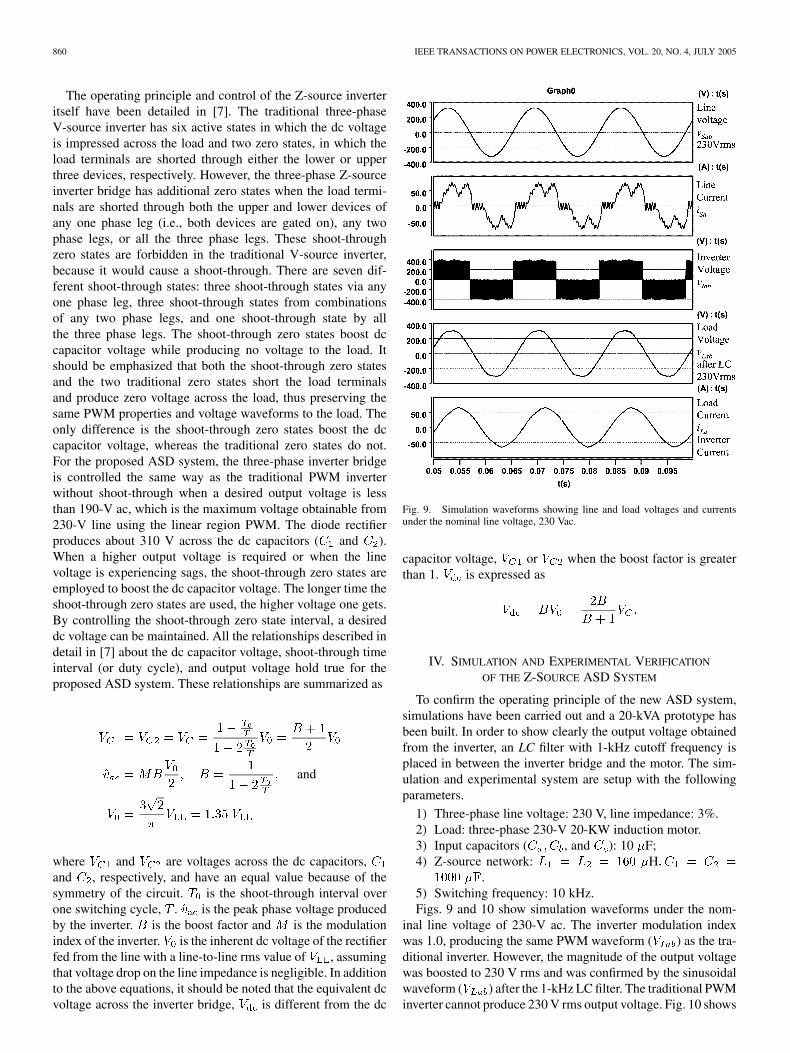
Fig. 9. Simulation waveforms showing line and load voltages and currentsunder the nominal line voltage, 230 Vac.
capacitor voltage, or when the boost factor is greaterthan 1. is expressed as
IV. SIMULATION AND EXPERIMENTAL VERIFICATION
OF THE Z-SOURCE ASD SYSTEM
To confirm the operating principle of the new ASD system,simulations have been carried out and a 20-kVA prototype hasbeen built. In order to show clearly the output voltage obtainedfrom the inverter, an LC filter with 1-kHz cutoff frequency isplaced in between the inverter bridge and the motor. The sim-ulation and experimental system are setup with the followingparameters.
1) Three-phase line voltage: 230 V, line impedance: 3%.2) Load: three-phase 230-V 20-KW induction motor.3) Input capacitors ( , and ): 10 F;4) Z-source network: H
.5) Switching frequency: 10 kHz.Figs. 9 and 10 show simulation waveforms under the nom-
inal line voltage of 230-V ac. The inverter modulation indexwas 1.0, producing the same PWM waveform ( ) as the tra-ditional inverter. However, the magnitude of the output voltagewas boosted to 230 V rms and was confirmed by the sinusoidalwaveform ( ) after the 1-kHz LC filter. The traditional PWMinverter cannot produce 230 V rms output voltage. Fig. 10 shows
PENG et al.: Z-SOURCE INVERTER FOR MOTOR DRIVES 861
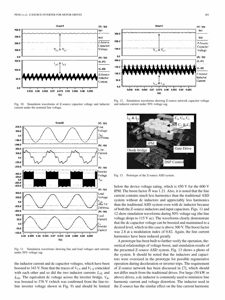
Fig. 10. Simulation waveforms of Z-source capacitor voltage and inductorcurrent under the nominal line voltage.
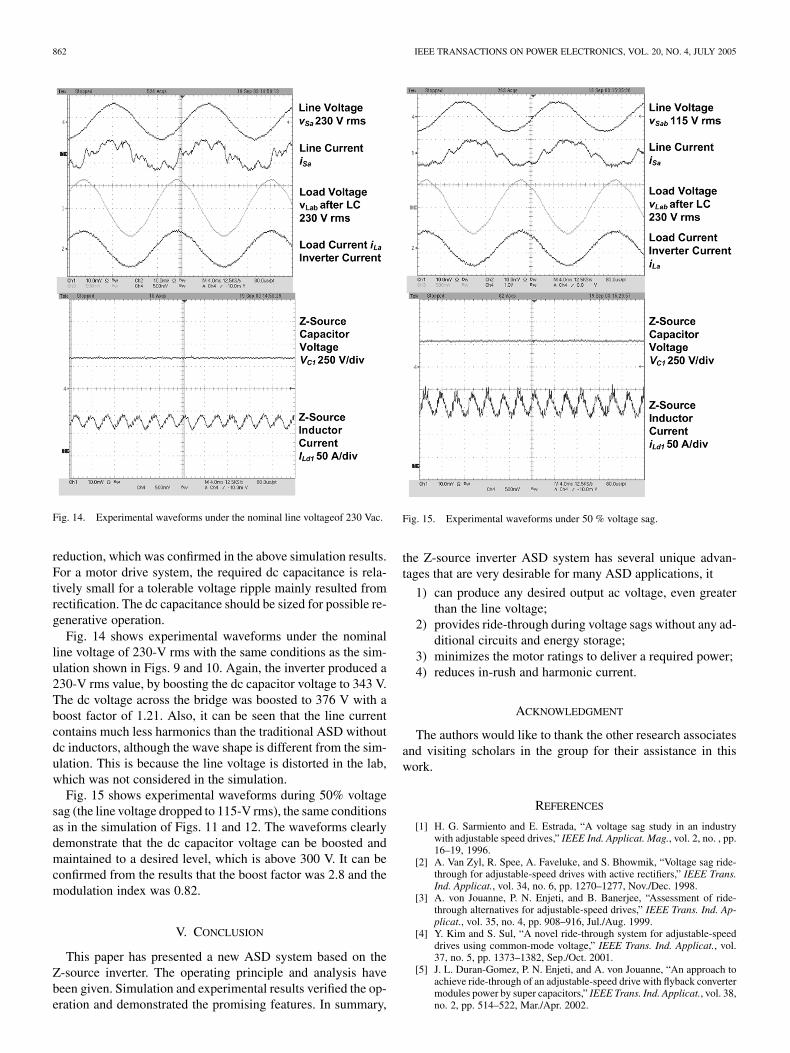
Fig. 11. Simulation waveforms showing line and load voltages and currentsunder 50% voltage sag.
the inductor current and dc capacitor voltages, which have beenboosted to 343 V. Note that the traces of and coincidedwith each other and so did the two inductor currents and
. The equivalent dc voltage across the inverter bridge,was boosted to 376 V (which was confirmed from the line-to-line inverter voltage shown in Fig. 9) and should be limited
Fig. 12. Simulation waveforms showing Z-source network capacitor voltageand inductor current under 50% voltage sag.
Fig. 13. Prototype of the Z-source ASD system.
below the device voltage rating, which is 450 V for the 600-VIPM. The boost factor was 1.21. Also, it is noted that the linecurrent contains much less harmonics than the traditional ASDsystem without dc inductors and appreciably less harmonicsthan the traditional ASD system even with dc inductor becauseof both the Z-source inductors and input capacitors. Figs. 11 and12 show simulation waveforms during 50% voltage sag (the linevoltage drops to 115 V ac). The waveforms clearly demonstratethat the dc capacitor voltage can be boosted and maintained to adesired level, which in this case is above 300 V. The boost factorwas 2.8 at a modulation index of 0.82. Again, the line currentharmonics have been reduced greatly.
A prototype has been built to further verify the operation, the-oretical relationships of voltage boost, and simulation results ofthe presented Z-source ASD system. Fig. 13 shows a photo ofthe system. It should be noted that the inductors and capaci-tors were oversized in the prototype for possible regenerativeoperation during deceleration or inverter trips. The requirementof Z-source network has been discussed in [7], which shouldnot differ much from the traditional drives. For large (50 kW orabove) drives, a dc inductor is commonly used to minimize lineharmonic current and voltage distortion. The inductor used inthe Z-source has the similar effect on the line current harmonic
862 IEEE TRANSACTIONS ON POWER ELECTRONICS, VOL. 20, NO. 4, JULY 2005
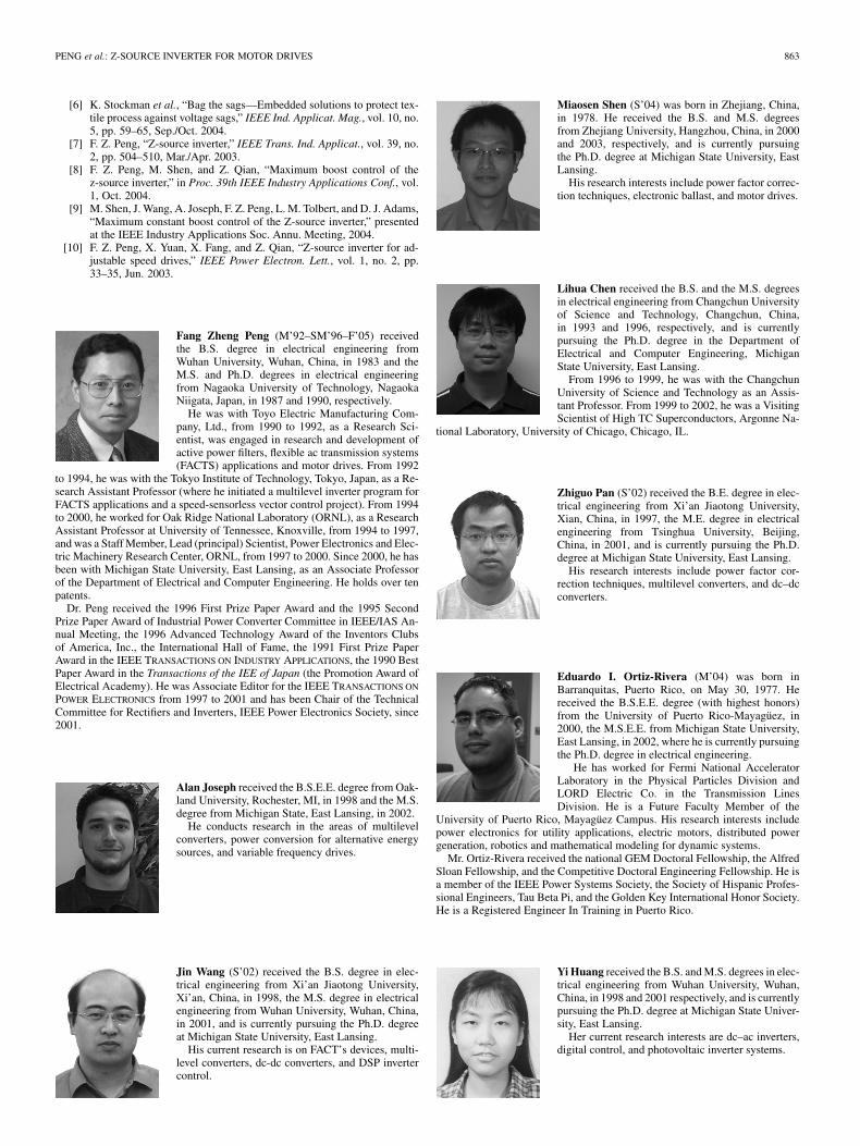
Fig. 14. Experimental waveforms under the nominal line voltageof 230 Vac.
reduction, which was confirmed in the above simulation results.For a motor drive system, the required dc capacitance is rela-tively small for a tolerable voltage ripple mainly resulted fromrectification. The dc capacitance should be sized for possible re-generative operation.
Fig. 14 shows experimental waveforms under the nominalline voltage of 230-V rms with the same conditions as the sim-ulation shown in Figs. 9 and 10. Again, the inverter produced a230-V rms value, by boosting the dc capacitor voltage to 343 V.The dc voltage across the bridge was boosted to 376 V with aboost factor of 1.21. Also, it can be seen that the line currentcontains much less harmonics than the traditional ASD withoutdc inductors, although the wave shape is different from the sim-ulation. This is because the line voltage is distorted in the lab,which was not considered in the simulation.
Fig. 15 shows experimental waveforms during 50% voltagesag (the line voltage dropped to 115-V rms), the same conditionsas in the simulation of Figs. 11 and 12. The waveforms clearlydemonstrate that the dc capacitor voltage can be boosted andmaintained to a desired level, which is above 300 V. It can beconfirmed from the results that the boost factor was 2.8 and themodulation index was 0.82.
V. CONCLUSION
This paper has presented a new ASD system based on theZ-source inverter. The operating principle and analysis havebeen given. Simulation and experimental results verified the op-eration and demonstrated the promising features. In summary,
Fig. 15. Experimental waveforms under 50 % voltage sag.
the Z-source inverter ASD system has several unique advan-tages that are very desirable for many ASD applications, it
1) can produce any desired output ac voltage, even greaterthan the line voltage;
2) provides ride-through during voltage sags without any ad-ditional circuits and energy storage;
3) minimizes the motor ratings to deliver a required power;4) reduces in-rush and harmonic current.
ACKNOWLEDGMENT
The authors would like to thank the other research associatesand visiting scholars in the group for their assistance in thiswork.
REFERENCES
[1] H. G. Sarmiento and E. Estrada, “A voltage sag study in an industrywith adjustable speed drives,” IEEE Ind. Applicat. Mag., vol. 2, no. , pp.16–19, 1996.
[2] A. Van Zyl, R. Spee, A. Faveluke, and S. Bhowmik, “Voltage sag ride-through for adjustable-speed drives with active rectifiers,” IEEE Trans.Ind. Applicat., vol. 34, no. 6, pp. 1270–1277, Nov./Dec. 1998.
[3] A. von Jouanne, P. N. Enjeti, and B. Banerjee, “Assessment of ride-through alternatives for adjustable-speed drives,” IEEE Trans. Ind. Ap-plicat., vol. 35, no. 4, pp. 908–916, Jul./Aug. 1999.
[4] Y. Kim and S. Sul, “A novel ride-through system for adjustable-speeddrives using common-mode voltage,” IEEE Trans. Ind. Applicat., vol.37, no. 5, pp. 1373–1382, Sep./Oct. 2001.
[5] J. L. Duran-Gomez, P. N. Enjeti, and A. von Jouanne, “An approach toachieve ride-through of an adjustable-speed drive with flyback convertermodules power by super capacitors,” IEEE Trans. Ind. Applicat., vol. 38,no. 2, pp. 514–522, Mar./Apr. 2002.
PENG et al.: Z-SOURCE INVERTER FOR MOTOR DRIVES 863
[6] K. Stockman et al., “Bag the sags—Embedded solutions to protect tex-tile process against voltage sags,” IEEE Ind. Applicat. Mag., vol. 10, no.5, pp. 59–65, Sep./Oct. 2004.
[7] F. Z. Peng, “Z-source inverter,” IEEE Trans. Ind. Applicat., vol. 39, no.2, pp. 504–510, Mar./Apr. 2003.
[8] F. Z. Peng, M. Shen, and Z. Qian, “Maximum boost control of thez-source inverter,” in Proc. 39th IEEE Industry Applications Conf., vol.1, Oct. 2004.
[9] M. Shen, J. Wang, A. Joseph, F. Z. Peng, L. M. Tolbert, and D. J. Adams,“Maximum constant boost control of the Z-source inverter,” presentedat the IEEE Industry Applications Soc. Annu. Meeting, 2004.
[10] F. Z. Peng, X. Yuan, X. Fang, and Z. Qian, “Z-source inverter for ad-justable speed drives,” IEEE Power Electron. Lett., vol. 1, no. 2, pp.33–35, Jun. 2003.
Fang Zheng Peng (M’92–SM’96–F’05) receivedthe B.S. degree in electrical engineering fromWuhan University, Wuhan, China, in 1983 and theM.S. and Ph.D. degrees in electrical engineeringfrom Nagaoka University of Technology, NagaokaNiigata, Japan, in 1987 and 1990, respectively.
He was with Toyo Electric Manufacturing Com-pany, Ltd., from 1990 to 1992, as a Research Sci-entist, was engaged in research and development ofactive power filters, flexible ac transmission systems(FACTS) applications and motor drives. From 1992
to 1994, he was with the Tokyo Institute of Technology, Tokyo, Japan, as a Re-search Assistant Professor (where he initiated a multilevel inverter program forFACTS applications and a speed-sensorless vector control project). From 1994to 2000, he worked for Oak Ridge National Laboratory (ORNL), as a ResearchAssistant Professor at University of Tennessee, Knoxville, from 1994 to 1997,and was a Staff Member, Lead (principal) Scientist, Power Electronics and Elec-tric Machinery Research Center, ORNL, from 1997 to 2000. Since 2000, he hasbeen with Michigan State University, East Lansing, as an Associate Professorof the Department of Electrical and Computer Engineering. He holds over tenpatents.
Dr. Peng received the 1996 First Prize Paper Award and the 1995 SecondPrize Paper Award of Industrial Power Converter Committee in IEEE/IAS An-nual Meeting, the 1996 Advanced Technology Award of the Inventors Clubsof America, Inc., the International Hall of Fame, the 1991 First Prize PaperAward in the IEEE TRANSACTIONS ON INDUSTRY APPLICATIONS, the 1990 BestPaper Award in the Transactions of the IEE of Japan (the Promotion Award ofElectrical Academy). He was Associate Editor for the IEEE TRANSACTIONS ON
POWER ELECTRONICS from 1997 to 2001 and has been Chair of the TechnicalCommittee for Rectifiers and Inverters, IEEE Power Electronics Society, since2001.
Alan Joseph received the B.S.E.E. degree from Oak-land University, Rochester, MI, in 1998 and the M.S.degree from Michigan State, East Lansing, in 2002.
He conducts research in the areas of multilevelconverters, power conversion for alternative energysources, and variable frequency drives.
Jin Wang (S’02) received the B.S. degree in elec-trical engineering from Xi’an Jiaotong University,Xi’an, China, in 1998, the M.S. degree in electricalengineering from Wuhan University, Wuhan, China,in 2001, and is currently pursuing the Ph.D. degreeat Michigan State University, East Lansing.
His current research is on FACT’s devices, multi-level converters, dc-dc converters, and DSP invertercontrol.
Miaosen Shen (S’04) was born in Zhejiang, China,in 1978. He received the B.S. and M.S. degreesfrom Zhejiang University, Hangzhou, China, in 2000and 2003, respectively, and is currently pursuingthe Ph.D. degree at Michigan State University, EastLansing.
His research interests include power factor correc-tion techniques, electronic ballast, and motor drives.
Lihua Chen received the B.S. and the M.S. degreesin electrical engineering from Changchun Universityof Science and Technology, Changchun, China,in 1993 and 1996, respectively, and is currentlypursuing the Ph.D. degree in the Department ofElectrical and Computer Engineering, MichiganState University, East Lansing.
From 1996 to 1999, he was with the ChangchunUniversity of Science and Technology as an Assis-tant Professor. From 1999 to 2002, he was a VisitingScientist of High TC Superconductors, Argonne Na-
tional Laboratory, University of Chicago, Chicago, IL.
Zhiguo Pan (S’02) received the B.E. degree in elec-trical engineering from Xi’an Jiaotong University,Xian, China, in 1997, the M.E. degree in electricalengineering from Tsinghua University, Beijing,China, in 2001, and is currently pursuing the Ph.D.degree at Michigan State University, East Lansing.
His research interests include power factor cor-rection techniques, multilevel converters, and dc–dcconverters.
Eduardo I. Ortiz-Rivera (M’04) was born inBarranquitas, Puerto Rico, on May 30, 1977. Hereceived the B.S.E.E. degree (with highest honors)from the University of Puerto Rico-Mayagüez, in2000, the M.S.E.E. from Michigan State University,East Lansing, in 2002, where he is currently pursuingthe Ph.D. degree in electrical engineering.
He has worked for Fermi National AcceleratorLaboratory in the Physical Particles Division andLORD Electric Co. in the Transmission LinesDivision. He is a Future Faculty Member of the
University of Puerto Rico, Mayagüez Campus. His research interests includepower electronics for utility applications, electric motors, distributed powergeneration, robotics and mathematical modeling for dynamic systems.
Mr. Ortiz-Rivera received the national GEM Doctoral Fellowship, the AlfredSloan Fellowship, and the Competitive Doctoral Engineering Fellowship. He isa member of the IEEE Power Systems Society, the Society of Hispanic Profes-sional Engineers, Tau Beta Pi, and the Golden Key International Honor Society.He is a Registered Engineer In Training in Puerto Rico.
Yi Huang received the B.S. and M.S. degrees in elec-trical engineering from Wuhan University, Wuhan,China, in 1998 and 2001 respectively, and is currentlypursuing the Ph.D. degree at Michigan State Univer-sity, East Lansing.
Her current research interests are dc–ac inverters,digital control, and photovoltaic inverter systems.