Embed Size (px)
Citation preview

2380 IEEE TRANSACTIONS ON POWER ELECTRONICS, VOL. 29, NO. 5, MAY 2014
Instability in Half-Bridge Circuits Switched WithWide Band-Gap Transistors
Andrew Lemmon, Member, IEEE, Michael Mazzola, Member, IEEE, James Gafford, Member, IEEE,and Christopher Parker, Student Member, IEEE
Abstract—Wide band-gap (WBG) field-effect devices are knownto provide a system-level performance benefit compared to sili-con devices when integrated into power electronics applications.However, the near-ideal features of these switching devices canalso introduce unexpected behavior in practical systems due to thepresence of parasitic elements. The occurrence of self-sustained os-cillation is one such behavior that has not received adequate studyin the literature. This paper provides an analytical treatment of thisphenomenon by casting the switching circuit as an unintentionalnegative resistance oscillator. This treatment utilizes an establishedprocedure from the oscillator design literature and applies it to theproblem of power circuit oscillation. A simulation study is providedto identify the sensitivity of the model to various parameters, andthe predictive value of the model is confirmed by experiment in-volving two exemplary WBG devices: a SiC vertical-channel JFETand a SiC lateral-channel MOSFET. The results of this study sug-gest that susceptibility to self-sustained oscillation is correlated tothe available power density of the device relative to the parasiticelements in the circuit, for which wide band-gap devices, to includeSiC and GaN transistors, are in a class approaching that of theradio frequency domain.
Index Terms—Gallium nitride, natural response, oscillation, sil-icon carbide, stability.
I. INTRODUCTION
R ECENT advances in the maturity of wide band-gap(WBG) semiconductors have increased the likelihood that
power electronics applications will begin to integrate this tech-nology on a large scale in the new few years, as designerscontinue to push for ways to improve the efficiency and powerdensity of their systems. Compared to their silicon counterparts,
Manuscript received February 15, 2013; revised May 10, 2013; acceptedJune 28, 2013. Date of current version January 10, 2014. This work was sup-ported by the Office of Naval Research as part of the Electric Ship Research andDevelopment Consortium under Grant N00014-08-1-0080. Recommended forpublication by Associate Editor P. (Guest AE-Wide Bandgap) Ranstad.
A. Lemmon was with the Center for Advanced Vehicular Systems (CAVS),Mississippi State University, Starkville, MS 39759 USA. He is now withthe University of Alabama, Tuscaloosa, AL 35487 USA (e-mail: [email protected]).
M. Mazzola is with the Department of Electrical and Computer Engineering,Center for Advanced Vehicular Systems (CAVS), Mississippi State University,Starkville, MS 39759 USA (e-mail: [email protected]).
J. Gafford is with the Center for Advanced Vehicular Systems(CAVS), Mississippi State University, Starkville, MS 39759 USA (e-mail:[email protected]).
C. Parker was with the Center for Advanced Vehicular Systems (CAVS), Mis-sissippi State University, Starkville, MS 39759 USA. He is now with RaytheonCorporation, Forest, MS 39074 USA (e-mail: [email protected]).
Color versions of one or more of the figures in this paper are available onlineat http://ieeexplore.ieee.org.
Digital Object Identifier 10.1109/TPEL.2013.2273275
WBG field-effect transistors are characterized by reduced con-duction losses, reduced switching losses, increased blockingvoltage, increased operating frequency, and increased toleranceto junction temperature. When these devices are properly de-signed into power electronics applications, their device-levelperformance advantages are known to produce a measurablesystem-level benefit in terms of efficiency and power density [1].These system-level benefits are unlocked, in large measure, dueto the fast-switching characteristics of WBG devices, whichpermit operation at high frequency without excessive switch-ing losses. However, the same fast-switching properties thatenable this system-level benefit can have other less desirableside-effects as well. One commonly reported complication en-countered in design of systems with WBG devices is the pres-ence of an undesirable level of under-damped natural response inthe application circuit [2]–[7]. The primary reason for this pro-nounced natural ring-down is the switching characteristics ofthe WBG transistors employed in these designs. As the switch-ing behavior of practical devices approaches that expected fromthe die dimensions at the unipolar limit of SiC and GaN transis-tors, the dV/dt and dI/dt observed during switching transientsincreases, and the amount of stray inductance in the power cir-cuit necessary to produce troublesome dynamics (ringing andoscillation) is reduced. For this reason, applications incorpo-rating high-performance, fast-switching WBG devices shouldbe designed in a manner that accounts for the consequencesof greater sensitivity to stray inductance. A second anomalythat can occur in circuits based on WBG devices is the oc-currence of unintended switching events. In a half-bridge cir-cuit, this behavior can manifest itself as shoot-through whenthe active switch turns on. In this case, dV/dt induced dis-placement current flows through the Miller capacitor into thegate drive of the inactive switch, which will result in Millerturn-on if the gate node rises to threshold. Alternatively, un-intended turn-on can result from an uncommanded rise in thegate–source voltage produced by negative dI/dt through thecommon source inductance during the turn-off of the activelygated switch. WBG-based systems are known to be at increasedrisk to both these sources of inadvertent switching due to theirfast switching times [8]. One further switching-related anomalythat has not received adequate study in the literature is the pos-sibility of self-sustained oscillation in circuits based on WBGdevices. An experimental example of this behavior observed ina SiC-based half bridge is shown in Fig. 1, and the circuit usedto generate these waveforms is presented in Fig. 2. It should benoted that the self-sustained oscillation phenomenon reported inthis paper is not caused by re-triggering of the gate-drive PWM
0885-8993 © 2013 IEEE. Personal use is permitted, but republication/redistribution requires IEEE permission.See http://www.ieee.org/publications standards/publications/rights/index.html for more information.

LEMMON et al.: INSTABILITY IN HALF-BRIDGE CIRCUITS SWITCHED WITH WIDE BAND-GAP TRANSISTORS 2381
Fig. 1. Half-bridge turn-off showing self-sustained oscillation. The initial loadcurrent for this experiment was approximately 40 A.
Fig. 2. Clamped inductive load test circuit used to generate waveforms inFig. 1. Parasitic elements are outlined with dashed boxes. Note that the top switchis not actively gated, but is biased OFF. The clamped inductor is represented asa current source.
signal. The occurrence of self-sustained oscillation is distinctfrom both the underdamped natural ring-down and the occur-rence of shoot-through. This distinction can be made primarilyon the basis of the fact that self-sustained oscillation is a per-petual phenomenon, whereas the other two anomalies are tran-sient events. Although the occurrence of natural ring-down or ofshoot-through can in some cases act as a “triggering” mechanismleading to the onset of self-sustained oscillation, the governingrelationships that underlie these phenomena are quite differ-ent and independent treatment is therefore warranted. Since theoccurrence of natural-ring down and shoot-through have beensufficiently addressed in the WBG device literature, the cur-rent work focuses exclusively on the third identified switchinganomaly, namely the possibility of self-sustained oscillation.
II. LITERATURE REVIEW
The phenomenon of self-sustained oscillation in circuitsbased on WBG semiconductors has not received a detailedtreatment in the literature at the time of this writing. Never-theless, occurrences of this problem have been reported severaltimes in the literature, and most of these reports have occurredduring the last one or two years as WBG device adoption has
accelerated. For example, Rodriguez et al. [9] report the occur-rence of self-sustained oscillation of GaN FETs during switch-ing characterization. Danilovic et al. [10] also report a switchingcharacterization effort with GaN devices that encountered self-sustained oscillation. Both SiC and GaN device manufacturershave also made reference to this phenomenon in their applica-tion literature. In a recent seminar by Efficient Power ConversionCorporation (EPC) [11], White report that gate-loop inductancepresent in GaN-based applications “can easily make an oscil-lator”. In an EPC application note [12], Abdoulin et al. warnpotential customers about the possibility of self-sustained deviceoscillation during pulsed curve tracer measurements. Other EPCapplication materials by Abdoulin et al. [13] and Strydom [14]further reinforce these warnings regarding self-sustained os-cillation and recommend minimizing the gate-loop inductancethrough careful layout and the use of the strip-line impedancematching design technique. Texas Instruments informs usersabout the possibility of gate-loop oscillation in the datasheet forits recently released GaN gate-drive IC, the LM5113 [15]. Creewarns of the possibility of self-sustained oscillation in a recentapplication note [16] and in the datasheet for the recently re-leased 1200 V, 100 A SiC MOSFET module [17]. None of thesepapers presents a detailed treatment of the self-sustained oscilla-tion phenomenon. Instead, these works serve primarily to notifyapplication designers of the possibility of this phenomenon andprovide experience-based hints for mitigation when this prob-lem is encountered.
Several other studies provide context relevant to the currentpaper, even though they do not explicitly reference the self-sustained oscillation phenomenon. For example, two papers byChen et al. [18], [19] provide an empirically based analysis ofthe parasitic elements that contribute to the pronounced naturalring-down in WBG applications. Other studies of the naturalring-down phenomenon are provided by Josifovic et al. [20]and Adamowicz et al. [21]. All of these papers indicate thatthe primary method available to designers for managing thenatural ring-down phenomenon is the reduction of switchingspeed. Indeed, two additional papers go so far as to claim thatthe aggregate inductance of the gate loop establishes a practicallimit to the switching frequency achievable in hard-switchedapplications [22], [23]. This is an important observation, as itreinforces the claim that high switching speed brings with it in-creased risk to the occurrence of various switching anomalies,of which self-sustained oscillation is an example. Analytical ex-pressions for the natural ring-down phenomenon in the powerloop are provided by Alatise et al. [24] and Wang et al. [25].The former paper is concerned primarily with the contributionof the anti-parallel diode to power loop natural ring-down. Theexpressions provided in the latter paper are more relevant to thecurrent paper, as they are based on an equivalent circuit thatincludes MOSFET intrinsic capacitances. However, [25] ex-cludes consideration of the gate-loop inductance, which rendersit inadequate to the task of describing the self-sustained oscil-lation phenomenon. Both [26] and [8] provide detailed analyt-ical treatments of the shoot-through switching anomaly, alongwith threshold criteria to avoid this behavior by reducing ei-ther switching speed or gate-loop parasitic inductance. Neither

2382 IEEE TRANSACTIONS ON POWER ELECTRONICS, VOL. 29, NO. 5, MAY 2014
of these sources attempts an analytical treatment of the natu-ral ring-down or self-sustained oscillation phenomena, but theequivalent circuit models used by both could serve as a basisfor such a treatment. Finally, in [27], Fujihira et al. present atheoretical treatment of a mode of parasitic-induced oscillationobserved during turn-off of a fast-switching silicon MOSFET. Inthis paper, even though the possibility of self-sustained oscilla-tion is not mentioned, the presented treatment follows a similarmethodology to that employed in the current paper. However, inorder to reduce the complexity of the analytical treatment, theauthors of [27] exclude consideration of the device gate-draincapacitance. The gate-drain capacitance represents an impor-tant intrinsic feedback mechanism present in any field-effectdevice that significantly influences the stability of FET-basedhalf-bridge circuits. This simplification limits the utility of theanalysis presented in [27] for predicting the possibility of half-bridge instability and makes it impossible to predict the busvoltage dependence of any observed oscillatory phenomena.
Several other papers that deal with switching anomalies inWBG-based systems may actually serve to perpetuate a generalconfusion regarding this topic. For example, in [28], Delaineet al. describe the design of a 1 MHz buck converter based onGaN devices that experiences several inter-related oscillatoryphenomena. Although it appears that the root cause of theseproblems is parasitic-induced oscillation, the authors refer to theoccurrence of EMC perturbation and radiated emissions as thesuspected cause. In another recent paper [29], Noguchi et al. alsopresent an analysis of the oscillatory modes observed in a 1 MHzhalf-bridge inverter. The authors conclude that the 80 MHz ring-ing observed in the system is the result of common mode noisecapacitively coupled into the gate drive circuit. While this is un-doubtedly a contributing factor to the observed problems, thereis also a significant measure of parasitic-induced oscillation thatgoes unexplained. In [30], Watanabe et al. provide an analysisof both the natural ring-down and shoot-through phenomenaobserved in a half-bridge switching test circuit. Unfortunately,the analysis in this paper does not cleanly separate these twophenomena and the result may be somewhat confusing to thereader. None of these papers deals with the phenomenon of self-sustained oscillation, although evidence of related oscillatoryphenomena is visible in each.
It should be noted that susceptibility to self-sustained oscil-lation is correlated with the performance of the WBG devicebeing employed. As Kaminski and Hilt report in [31], current-generation GaN HFETs and SiC vertical-channel JFETs are theonly commercially available WBG devices with performanceapproaching the 4 H SiC unipolar limit. These two categoriesalso represent the devices that are most commonly reportedto experience self-sustained oscillation. Thus, the WBG deviceswith the highest-available performance are also the devices withthe greatest susceptibility to self-sustained oscillation. This canbe explained in part by the very low specific on-resistance ofthese devices. The small die size of these devices results insupport for very fast switching: SiC vertical channel JFETswere recently reported to switch 20 A at 600 V at speeds ofgreater than 30 V/ns [32]; GaN HFETs were recently reportedto switch 20 A at 350 V at speeds of 80 V/ns [7]. Commercially
available SiC lateral-channel MOSFETs, on the other hand, havereduced susceptibility to self-sustained oscillation. The compa-rably higher specific on-resistance of this topology means thatpractical devices have larger die area than similarly rated SiCvertical-channel JFETs and GaN HFETs [1], [33], [34]. Thecomparably higher intrinsic capacitance of the SiC lateral chan-nel MOSFET not only reduces the switching speed available toapplications with similar gate drive capability, but also providesa self-snubbing effect that serves to further reduce susceptibilityto self-sustained oscillation, at the cost of increased switchinglosses and/or gate drive power. Nevertheless, the lateral channelSiC MOSFET is not immune as this device has been reportedto experience self-sustained oscillation as well [16], [17].
III. THEORETICAL ANALYSIS
In order to provide a means by which power electronicspractitioners can deterministically eliminate the possibility ofself-sustained oscillation from occurring in their applications, acomprehensive theoretical treatment of this phenomenon is re-quired. One reference that provides a qualitative description ofthe natural ring-down phenomenon does so by breaking downthis behavior into two components: (1) the initial storage of en-ergy in the power loop resonant tank, which is observable as avoltage overshoot, and (2) the damped oscillatory ring-down asthis energy storage is dissipated in the power loop equivalentseries resistance [35]. Although the mechanisms that govern theself-sustained oscillation are different from this description, thiscompartmentalization of the resonant behavior is attractive fordescribing the self-sustained oscillation phenomenon as well.One reason why this is true is that the underlying conditionsthat enable these two modes appear to be separate. As will bedescribed in Section V, it is possible to create an initial cycle thatis favorable to self-sustained oscillation without creating a self-sustained oscillator. This compartmentalization also permits theanalysis of the second phase of oscillation to occur at a higherlevel of abstraction, which is in agreement with an establishedconstruct found in the literature. Therefore, this logical sepa-ration of this behavior into an initial cycle and the subsequentoscillatory behavior will be adopted for the remainder of thispaper following the analytical treatment first published by theauthors in [36]. The previous work represented a special caseapplicable to SiC JFETs that exhibit negligible drain–sourcecapacitance. The formulation presented here is generalized toinclude the effect of drain–source capacitance, and is thereforeapplicable to any field-effect device, without regard for devicetopology.
A. Initial Cycle
The behavior of the clamped-inductive-load test circuit ofFig. 2 during the initial cycle of oscillation can be understoodby considering the simplified equivalent circuit shown in Fig. 3.A positive dV/dt is expressed across the drain and source ter-minals of the active switch when it is gated off; a similar voltageslew is seen by the inactive switch in a half-bridge circuit whenthe active switch is gated on. In either case, this positive dV/dtcauses displacement current (IG ) to flow through the Miller
LEMMON et al.: INSTABILITY IN HALF-BRIDGE CIRCUITS SWITCHED WITH WIDE BAND-GAP TRANSISTORS 2383
Fig. 3. Equivalent circuit of power FET during positive dV/dt event atturn-off.
Fig. 4. Notional gate–source ring-back to threshold during initial cycle ofnatural ring-down.
capacitance (C1) of the device with the polarity indicated inFig. 3. This displacement current must be sunk by the gate drivein order to prevent inadvertent turn-on of the device. During thisprocess, the gate inductance (LG ) stores energy, which must bedissipated in order for the gate–source voltage to settle at thegate-drive low-line potential (−VSS ). The presence of nonnegli-gible device input capacitance as represented (primarily) by C2means that the gate–source voltage will exhibit a second-orderring-down as the resonant tank formed by LG and C2 is depletedof energy by dissipation in the gate resistor (RG ). It is importantto recognize that WBG circuits intended for fast switching typ-ically utilize a small RG value. There are two reasons for this.First, a small RG value is required to enable rapid charging anddischarging of the FET input capacitance. Second, a small valuefor RG also reduces the susceptibility of the circuit to Millerturn-on because it improves the ability of the gate-drive circuitto quickly sink displacement current. However, the selectionof a small RG value has an additional unintended side-effect:it results in an underdamped gate loop in the presence of anystray gate inductance. As a result, the positive dV/dt event thatoccurs during every switching cycle has the potential to pro-duce an underdamped gate-loop natural ring-down. When thisoccurs, the first time the gate–source voltage rings back above−VSS there is the possibility that the gate potential may reachthe threshold voltage and the device may turn back on, as de-picted in Fig. 4. The resulting channel conduction creates anadditional current path, which is represented by the dependentcurrent source in Fig. 3. If ring-back falls short of the thresholdvoltage, then self-sustained oscillation is not possible. If ring-back to threshold occurs, then the resulting channel conductionwill distort the natural response of the two-mesh circuit such
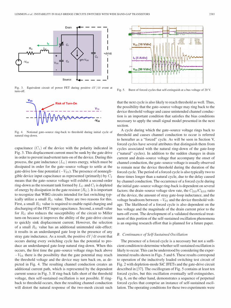
Fig. 5. Burst of forced cycles that self-extinguish at a bus voltage of 20 V.
that the next cycle is also likely to reach threshold as well. Thus,the possibility that the gate–source voltage may ring back to thedevice threshold voltage and cause unintended channel conduc-tion is an important condition that satisfies the bias conditionsnecessary to apply the small signal model presented in the nextsection.
A cycle during which the gate–source voltage rings back tothreshold and causes channel conduction to occur is referredto hereafter as a “forced” cycle. As will be seen in Section V,forced cycles have several attributes that distinguish them fromcycles associated with the natural ring-down of the gate-loop(“natural” cycles). In addition to the sudden changes in draincurrent and drain–source voltage that accompany the onset ofchannel conduction, the gate–source voltage is usually observedto remain near the device threshold during the duration of theforced cycle. The period of a forced cycle is also typically two tothree times longer than a natural cycle, due to the delay causedby channel conduction. The occurrence of a forced cycle duringthe initial gate–source voltage ring-back is dependent on severalfactors: the drain–source voltage slew rate, the CISS /CRSS ratioof the device, the amount of stray gate-loop inductance, and thevoltage headroom between −VSS and the device threshold volt-age. The likelihood of a forced cycle is also dependent on thebus voltage and the magnitude of the drain current prior to theturn-off event. The development of a validated theoretical treat-ment of this portion of the self-sustained oscillation phenomenais an ongoing research effort that is planned for a future paper.
B. Continuance of Self-Sustained Oscillation
The presence of a forced cycle is a necessary but not a suffi-cient condition to determine whether self-sustained oscillation islikely to occur. This can be understood by considering the exper-imental results shown in Figs. 5 and 6. These results correspondto operation of the inductively loaded switching test circuit ofFig. 2 with depletion-mode SiC JFETs and the gate-drive circuitdescribed in [37]. The oscillogram of Fig. 5 contains at least tenforced cycles, but this oscillation eventually self-extinguishes.Fig. 6, on the other hand, demonstrates a sequence of perpetualforced cycles that comprise an instance of self-sustained oscil-lation. The operating conditions for these two experiments were

2384 IEEE TRANSACTIONS ON POWER ELECTRONICS, VOL. 29, NO. 5, MAY 2014
Fig. 6. Sequence of forced cycles comprising an instance of self-sustainedoscillation at a bus voltage of 25 V.
Fig. 7. Notional small-signal model for negative conductance oscillator.
identical with the exception of the bus voltage applied. It can beconcluded that some additional mechanism beyond the presenceor absence of forced cycles is necessary in order to predict thepossibility of self-sustained oscillation.
In contrast to the occurrence of a damped natural-response,the phenomenon of self-sustained oscillation cannot be at-tributed solely to the exchange of energy between parasiticelements. The self-sustaining nature of the oscillation shownin Fig. 6 implies that the energy dissipated by parasitic resis-tance in the circuit during each cycle is replaced by a feedbackmechanism drawing energy from the bus. An established con-ceptual framework for describing this process common in theoscillator design community is the negative resistance (or neg-ative conductance) model [38], [39]. One of the contributionsof the current paper is the recognition that the WBG field-effectdevice and its associated parasitic elements can be re-cast asan unintentional negative-resistance oscillator. The advantagesof this approach are that it leverages a well-established for-malism for describing the propensity of a circuit to oscillateindefinitely, and it provides a higher level of abstraction that isuseful for making predictions about practical power electronicsapplications.
According to the negative conductance formulation, the os-cillator is represented as a single port network composed oftwo-branches: a “motional” branch and an “active” branch. Inthe case of a traditional linear oscillator circuit, the motionalbranch is implemented with a crystal, and the active branch isimplemented with a transistor and an appropriate bias circuit.This abstraction of the notional oscillator circuit is shown inFig. 7. As a practical matter, the operation of the notional oscil-lator can be understood by recognizing that susceptances BOSC
Fig. 8. Small-signal model of unintentional WBG transistor oscillator.
and BM collectively form a resonant tank and the positive con-ductance GM extracts energy from this tank during each cycleof oscillation. The “negative conductance” represented in theactive branch is a circuit that is capable of adding energy backto the resonant tank from an external source. Negative conduc-tance is a convenient abstraction that permits the overall stabilityof this circuit to be described in terms of energy transfer ratherthan through circuit analysis methods.
In order for the notional two-branch oscillator shown in Fig. 7to achieve constant-envelope oscillation, the following two con-ditions must be satisfied: 1) the susceptance in the motionalbranch must be canceled by an opposite-signed and equal-magnitude susceptance in the active branch (BM = −BOSC);and 2) the positive conductance in the motional branch must becanceled by an equal-magnitude negative conductance in the ac-tive branch (GM = −GOSC). In the oscillator design literature,small-signal models are commonly used to predict the occur-rence of self-sustained oscillation at a given operating point byevaluating these two criteria [39], [40]. In the case of the unin-tentional WBG transistor oscillator, the physical circuit shownin Fig. 2 can be abstracted into a small-signal negative con-ductance oscillator model suitable for the application of thisanalysis procedure. This is accomplished by removing indepen-dent voltage and current sources and reflecting the power loopparasitic components LD and RESR as parallel equivalents, as-suming that ωLD � RESR . In the case of the high-side switch,the anti-parallel rectifier clamps the current source followingturn-off of the low-side switch and thus is a short circuit in thesmall signal model. The small-signal model that results fromthis process is shown in Fig. 8. In this representation, the activebranch is represented by the equivalent circuit of the WBG tran-sistor and its associated gate drive circuit; the motional branchis represented by the power loop parasitic elements. With theindependent sources removed, the reactance of the power loopis predominantly inductive, while the reactance of the activebranch is predominantly capacitive.
By considering the admittance seen from YIN , it can be seenthat satisfying the first condition for oscillation implies thatIm {YIN} = 0 since YIN incorporates the reactive portions ofboth motional and active branches. This relationship is satisfiedat one or more frequencies, which represent the resonant modesof the system. Satisfying the second condition for constant-envelope oscillation implies that Re {YIN} = −GEP . This con-dition determines the envelope of oscillation. In practice, eval-uation of the second condition is what determines whether the

LEMMON et al.: INSTABILITY IN HALF-BRIDGE CIRCUITS SWITCHED WITH WIDE BAND-GAP TRANSISTORS 2385
Fig. 9. Annotated small-signal WBG oscillator equivalent circuit.
WBG oscillator will sustain oscillation or not. Three possi-bilities can result from the evaluation of this second condi-tion. When Re {YIN} > −GEP , the model predicts an oscil-lation envelope with decreasing magnitude over time; whenRe {YIN} = −GEP , the model predicts constant-envelope os-cillation; and when Re {YIN} < −GEP , the model predicts anoscillation envelope with increasing magnitude over time. How-ever, in practice, it is found that the unintentional WBG oscilla-tor will either experience self-extinguishing oscillation if insuf-ficient negative conductance is available (Re {YIN} > −GEP)or self-sustained oscillation if sufficient negative conductance isavailable (Re {YIN} ≤ −GEP). The increasing-envelope caseultimately collapses into the constant-envelope case becausenonlinearities present in a practical circuit prevent the ampli-tude of oscillation from increasing indefinitely. This automaticestablishment of equilibrium is a well-known principle that isrelied upon in intentional oscillator design to ensure proper os-cillator start-up [38].
An analytical expression for YIN can be readily derived byconsidering the annotated form of the small signal model pre-sented in Fig. 9. In this form, the following equalities are estab-lished: X1 = 1/ (jωC1) ,X2 = 1/ (jωC2) ,XD = jωLD , andZG = RG + jωLG .
First, an expression for ZX is created
ZX = X1 +ZGX2
ZG + X2. (1)
The voltage across X2 is then found by voltage division
V2 = V1 ·ZGX2/(ZG + X2)
X1 + ZGX2/(ZG + X2). (2)
Writing Kirchhoff’s current law (KCL) for the node labeled“A” produces the following expression:
−i1 + gm V2 +V1
ZX= 0. (3)
Substituting (3) into an expression for Y1 produces the fol-lowing result:
Y1 =I1
V1= gm
V2
V1+
1ZX
. (4)
Substituting (1) and (2) into (4) and multiplying by (ZG +X2)/ZGX2 yields the following result:
Y1 =gm + ((ZG + X2)/ZGX2)X1 (ZG + X2) /ZGX2 + 1
. (5)
Finally, the expression for YIN can be obtained by combiningY1 with X3 and XD :
YIN =gm + (ZG + X2)/ZGX2
X1 (ZG + X2) /ZGX2 + 1+
1X3
+1
XD. (6)
Equation (6) can be used to determine the susceptibility ofa particular circuit to self-sustained oscillation by followinga two-part analysis procedure. The resonant frequency of thecircuit is first determined by solving for the roots of the equationIm {YIN} = 0. For the general case of (6) in which none of thecomponents are negligible, separating the imaginary portionof YIN produces a cubic equation in terms of ω2 . Thus, threeindependent solutions for |ω| are possible, and each solution is avalid resonant frequency for the small-signal model. However, ithas been determined through empirical analysis that the solutionthat matches the observable resonant frequency of the circuit isthe lowest of the three solutions. Once the applicable resonantfrequency is determined, this value is substituted into Re {YIN}and the result is compared to −GEP . If Re {YIN} ≤ −GEP ,the specified set of circuit parameters is predicted to produceself-sustained oscillation.
The model presented here is flexible enough to provide usefulinformation to designers regarding the propensity of practicalcircuits to experience self-sustained oscillation. Since this pre-dictive ability is based on a small-signal model, it is by definitiondependent upon the selection of an operating point. However, theoperating conditions of the circuit are not explicitly representedin the formulation given by (6), so it may not be immediatelyapparent how an operating point is chosen for analysis. This isdone implicitly through the selection of circuit parameter val-ues. For instance, the Miller capacitance of a field effect deviceis known to be a nonlinear function of the drain–source voltage.Therefore, model value C1 is chosen to represent the Millercapacitance associated with a particular WBG device linearizedaround a particular drain–source bias. Likewise, the model val-ues C2 and gm are selected to represent linearized values for agiven device around a gate–source voltage bias near the thresh-old voltage. The operating point dependence of the model doesnot limit its utility for predicting the likelihood of self-sustainedoscillation across a wide range of operating points. One reason isthe physical reality of this quasi-static condition imposed by thenature of the circuit involved, which is a half-bridge switchinga clamped inductive load on a constant voltage bus. The oscilla-tion in question occurs after commutation of the switch currentto the opposite leg of the half bridge where the central tendencyof the oscillating drain source voltage is the bus value. A sec-ond reason is that the gate–source voltage is clamped at or nearthe threshold voltage by displacement current flowing throughthe Miller capacitance when the channel begins to conduct; afact empirically established in Section V. The implementationused by the authors incorporates a look-up table of Miller ca-pacitance values vs. drain–source bias for several specific WBGdevices. By leveraging this information, a specific set of circuitparasitic values can be evaluated across a range of drain–sourcevoltages to determine susceptibility to self-sustained oscillationas a function of voltage.

2386 IEEE TRANSACTIONS ON POWER ELECTRONICS, VOL. 29, NO. 5, MAY 2014
TABLE IPARAMETER VALUES FOR SIMULATION STUDY
Fig. 10. Evaluation of RG NORM dependence for SiC JFET profile. Notethat gm is fixed at a nominal value of 10 mS.
IV. SIMULATION STUDY
As part of this paper, a simulation study was performed toevaluate the sensitivity of the model to various model parame-ters. It has been shown in a previous work that susceptibility toself-sustained oscillation increases with increased transconduc-tance, and with reduced gate-loop damping expressed as the nor-
malized gate resistance, RG NORM = RG/[√
LG/C2
]= 2ζ,
where ζ is the damping ratio of the gate loop [36]. In the currentpaper, the simulation study was designed to elucidate the im-plications of selecting a WBG transistor with a particular ratioof input capacitance to Miller capacitance. For this reason, thesame simulation profile was executed with values correspond-ing to two test fixtures: one configured to evaluate a SiC JFETwith a CISS /CRSS ratio of approximately 3 at 100 V drain–source bias, and one configured to evaluate a SiC MOSFETwith a CISS /CRSS ratio of approximately 80 at 100 V drain–source bias. The specific parameter values used to populate thesimulation for each test are presented in Table I.
In each of the following plots, the ordinate represents a nor-malized conductance figure of merit Re {YIN} /GEP , whichpermits identification of the region of susceptibility to self-sustained oscillation. In these plots, any portion of the con-ductance curve that exists at or below the −1 point represents aregion of susceptibility to self-sustained oscillation. The systemsensitivity to the value of normalized gate resistance for the SiCJFET and the SiC MOSFET can be observed in Figs. 10 and11, respectively. As anticipated from the previous work, bothdevices are more susceptible to self-sustained oscillation at
Fig. 11. Evaluation of RG NORM dependence for SiC MOSFET profile. Notethat gm is fixed at a nominal value of 7 mS.
Fig. 12. Evaluation of gm dependence for SiC JFET profile. Note thatRG NORM is fixed at a nominal value of 0.068.
Fig. 13. Evaluation of gm dependence for SiC MOSFET profile. Note thatRG NORM is fixed at a nominal value of 0.060.
small values of normalized gate resistance. However, the shapeof the normalized conductance curves is instructive to com-pare. The SiC MOSFET, which has a higher CISS /CRSS ratio,creates a narrower region of susceptibility at a lower drain–source voltage than the SiC JFET. This is due to the fact that thehigher CISS /CRSS ratio of the SiC MOSFET results in a scal-ing factor that compresses the normalized conductance curvestoward lower drain–source voltage. A similar trend is evidentin Figs. 12 and 13, which represent the system sensitivity to thevalue of FET transconductance for the SiC JFET and the SiCMOSFET, respectively. As anticipated from the previous work,

LEMMON et al.: INSTABILITY IN HALF-BRIDGE CIRCUITS SWITCHED WITH WIDE BAND-GAP TRANSISTORS 2387
higher transconductance near threshold results in increased sus-ceptibility to self-sustained oscillation. In addition, the samescaling trend is evident in the case of the SiC MOSFET, re-sulting in a narrower region of susceptibility at lower voltagewhen compared to the SiC JFET. However, it should also benoted that the SiC MOSFET creates a more gradual increase innormalized conductance with increased drain–source voltage atgm values >5 mS. Thus, the SiC MOSFET could be describedas having two separate regions of susceptibility: a severe regionof susceptibility at low voltages, and a somewhat less severe butbroader region of susceptibility at moderate voltages.
V. EMPIRICAL STUDY
As part of the current paper, an empirical study was conductedto evaluate the predictive performance of the small signal modelpresented in Section III. This effort consisted of executing a se-ries of clamped-inductive-load tests using a switching circuitsimilar to that shown in Fig. 2. As in the previous section, both aSiC depletion-mode JFET and a SiC MOSFET were evaluatedso that the device topology implications on the susceptibility toself-sustained oscillation could be validated. For the SiC JFETcircuit, a gate-drive evaluation module available from the man-ufacturer was utilized [41]; for the SiC MOSFET circuit, themanufacturer’s recommended gate-drive design was followedincluding layout suggestions [42]. No attempt was made to op-timize the gate drive for either circuit beyond following themanufacturer recommendations. For each test circuit, the fol-lowing procedures were utilized in order to determine the ef-fective circuit values for use in populating the simulation. Theeffective power loop conductance GEP was determined by di-rect observation of the damping ratio. Small coils of wire wereused to construct LD and LG , which were characterized usinga Wayne–Kerr precision magnetics analyzer and a custom testfixture suitable for the low inductance involved. The chosen val-ues were selected in order to dominate over the stray inductanceon the test board but are not unrealistic levels found in manyapplications [43]. The parameter that was used as a degree offreedom for curve-fitting purpose was the FET transconductancegm . This parameter value cannot be considered to be firmly heldconstant for all tests, since device transconductance varies withgate–source voltage and the value of gate–source voltage ring-back varies slightly from test to test. However, the small rangeof values used for each device is known to be consistent withmeasured transconductance values at a gate–source voltage biasnear the threshold voltage. The full set of parameter values thatwere measured in the two test fixtures and used to populate thecorresponding simulations are given in Table II.
As has been pointed out in Section III, it is important thatthe initial cycle of oscillation establishes the bias conditionsnecessary to properly apply the small signal model upon whichthe susceptibility prediction is based. For this reason, a prelim-inary set of switching experiments was conducted in order todetermine the conditions under which the initial cycle wouldestablish the appropriate bias conditions. The two primary fac-tors that influence the initial ring-back to threshold are thedrain–source voltage and the magnitude of the drain current
TABLE IIEMPIRICAL STUDY MODEL PARAMETERS
Fig. 14. Establishment of bias conditions for small-signal model during initialcycle of oscillation.
prior to the turn-off event. The drain–source voltage has a non-linear impact on the establishment of bias conditions, but it hasbeen determined that providing an adequate level of drain cur-rent prior to the turn-off event permits the establishment of theproper bias conditions across a wide range of drain–source volt-ages. An example of the establishment of the proper bias condi-tions for the SiC JFET test circuit can be seen in Fig. 14. Notethat during the initial cycle of oscillation, the gate–source volt-age rings back to the device threshold voltage. Time correlatedwith reaching threshold is the observation of a disturbance inthe drain–source voltage. This perturbation in the drain–sourcevoltage is direct evidence of channel conduction and nonzerotransconductance, and justifies the bias condition necessary forapplication of the small signal model. Once this bias conditionis established, the small-signal model is valid and can be usedto predict whether the oscillatory behavior is likely to continueindefinitely or not.
A. Empirical Results for SiC Lateral-Channel DMOSFET
A summary of the empirical results for the SiC MOSFET testsequence is plotted in histogram format along with the normal-ized conductance curves determined by simulation in Fig. 15.From this figure, it can be determined that the small signalmodel provides good quantitative agreement with the empirical

2388 IEEE TRANSACTIONS ON POWER ELECTRONICS, VOL. 29, NO. 5, MAY 2014
Fig. 15. Empirical results comparison to simulation output for SiC MOSFET.
results based on an envelope of transconductance values thatare reasonable for the value of gate–source voltage ring-backobserved in these experiments. It is also apparent that the SiCMOSFET does not experience self-sustained oscillation acrossthe envelope of test cases evaluated, but the device does expe-rience a number of forced cycles during the low-voltage regionof susceptibility. This behavior is predicted by the model in thatthe normalized conductance approaches, but does not cross the-1 point. It should also be pointed out that the second region ofsusceptibility predicted by the model for the SiC MOSFET isalso confirmed by experimental evidence in the 30–60 V range.Example time-domain waveforms for SiC MOSFET tests from10 to 40 V are given in Fig. 16. From this plot it is apparentthat the presence of negative conductance distorts the naturalresponse of the drain–source voltage and results in unintendedchannel conduction in the device. The number of forced cyclespresent in each of the subplots in this figure corresponds withthe histogram summary in Fig. 15. In addition, Fig. 17 presentsa comparison of the frequency of forced oscillation predictedby the model and measured in experiment for a range of op-erating conditions. Note that the natural resonant frequency ofthe power loop in this test circuit is significantly higher thanthe frequency of forced oscillation at any operating conditionconsidered. This fact confirms the separation of these two phe-nomena and corroborates the validity of the analytical model.
B. Empirical Results for SiC Vertical-Channel JFET
A summary of the empirical results for the SiC JFET test se-quence is plotted in histogram format along with the normalizedconductance curves determined by simulation in Fig. 18. Fromthis figure, it can be determined that the small signal modelagain provides good quantitative agreement with the empiricalresults based on an envelope of transconductance values thatare reasonable for the value of gate–source voltage ring-backobserved in these experiments. It can also be observed from thisfigure that the SiC JFET-based circuit oscillates in a region of
Fig. 16. SiC MOSFET experimental waveforms at several different bus volt-age values. One forced cycles is evident at 10 V; four forced cycles are evidentat 20 V; and two forced cycles are evident at 40 V.
Fig. 17. Comparison of natural and forced frequencies for SiC MOSFET testcircuit. The natural resonant frequency of the power loop (upper line) is widelyseparated from the frequency of forced oscillation predicted by the model (lowerline) and measured in experiment (circle markers).

LEMMON et al.: INSTABILITY IN HALF-BRIDGE CIRCUITS SWITCHED WITH WIDE BAND-GAP TRANSISTORS 2389
Fig. 18. Empirical results comparison to simulation output for SiC JFET.
susceptibility around 30 V, as predicted by the model. Exampletime-domain waveforms for SiC JFET tests from 10 to 40 Vare given in Fig. 19. From this plot it is apparent that the pres-ence of negative conductance distorts the natural response of thedrain–source voltage as a result of unintended channel conduc-tion in the device. The number of forced cycles present in eachof the subplots in this figure corresponds with the histogramsummary in Fig. 18. In addition, Fig. 20 presents a comparisonof the frequency of forced oscillation predicted by the modeland measured in experiment for a range of operating conditions.Note that the natural resonant frequency of the power loop in thistest circuit is significantly higher than the frequency of forcedoscillation at any operating condition considered. This fact con-firms the separation of these two phenomena and corroboratesthe validity of the analytical model.
C. Comparison of SiC MOSFET and SiC JFETEmpirical Results
Several instructive inferences can be made based on the re-sults presented in the previous two sections. For example, itcan be stated that the lateral-channel SiC MOSFET is generallyless susceptible to the occurrence of self-sustained oscillationthan the vertical-channel SiC JFET for the range of parasiticvalues considered. This can be explained in part by the factthat the performance of the SiC MOSFET is farther from idealSiC unipolar switch behavior when compared to the SiC JFETdue to its higher specific on-resistance. As a result of this per-formance difference, the SiC MOSFET has significantly largerdie area, and therefore higher intrinsic capacitances, than theSiC JFET. The larger intrinsic capacitances provide the SiCMOSFET with a substantial self-snubbing capability, which hasthe effect of reducing its susceptibility to self-sustained oscilla-tion. The SiC MOSFET also switches more slowly than the SiCJFET, which further reduces its susceptibility to self-sustainedoscillation. However, as this paper has pointed out, the like-lihood of self-sustained oscillation is correlated to switching
Fig. 19. SiC JFET experimental waveforms at several different bus voltagevalues. Three forced cycles are evident at 10 V; self-sustained oscillation isevident at 25 V; and nine forced cycles are evident at 40 V.
Fig. 20. Comparison of natural and forced frequencies for SiC JFET testcircuit. The natural resonant frequency of the power loop (upper line) is widelyseparated from the frequency of forced oscillation predicted by the model (lowerline) and measured in experiment (circle markers).

2390 IEEE TRANSACTIONS ON POWER ELECTRONICS, VOL. 29, NO. 5, MAY 2014
performance, and therefore advanced device topologies suchas the SiC trench MOSFET are more likely to be at risk toself-sustained oscillation. In fact, any device that is capableof switching at high voltage and current slew rates is at riskof experiencing this problem, which explains the prominence ofwarnings in the GaN device literature. The specific likelihood ofoccurrence for a given device and circuit can be predicted basedon the procedure outlined in this paper, but the general trend evi-dent in the current paper is that higher-speed, lower-capacitancedevices are more likely to experience this problem than lower-speed, higher capacitance devices in power electronic circuitsdesigned without this consideration in mind.
VI. METHODS FOR MITIGATION OF
SELF-SUSTAINED OSCILLATION
Several methods are available for reducing the risk of self-sustained oscillation. The most fundamental method is the re-duction of stray gate-loop inductance. This should be consid-ered a basic design goal for any application attempting to oper-ate WBG devices at the maximum achievable switching speed.However, since stray inductance cannot be completely elimi-nated in practical circuits, it may be necessary to augment thisstrategy, particularly when attempting to maximize the switch-ing speed of WBG devices. The only additional solution in theliterature for reducing the risk of self-sustained oscillation is thereduction of switching speed. However, this strategy erodes thebenefit of WBG device adoption, and is therefore not an attrac-tive solution for advanced power electronics applications. In thecase that the reduction of switching speed is accomplished byincreasing the value of the series gate resistance, this solutionalso increases the risk of Miller turn-on (and shoot-through inhalf-bridge circuits). Clearly, better techniques are needed toreduce the susceptibility of applications to self-sustained os-cillation without trading away the low-loss switching behaviorthat is one of the major attractions of WBG devices. In the caseof the SiC vertical-channel JFET with negligible drain–sourcecapacitance, one effective solution is to add a small ballastingcapacitor across the gate–source terminals, close to the die. Thisadditional capacitance has an effect on the conductance curvessimilar to that observed when the normalized gate resistance isincreased as shown in Fig. 10. However, in the case of addingexternal gate–source capacitance, the stabilizing effect does notdepend on the reduction of switching speed, and it has the an-cillary benefit of reducing the risk of Miller turn-on. In thecase of a device with significant drain–source capacitance suchas the SiC DMOSFET, the addition of a ballasting capacitoracross the gate–source terminals has a more complex relation-ship on stability. In this case, the amount of external capacitancerequired to produce a stabilizing effect is greater than that re-quired for the device with negligible drain–source capacitance.In addition, the stabilizing effect is not universal and small val-ues of external gate–source capacitance may actually produce ade-stabilizing effect. This result also holds true for the vertical-channel JFET when an anti-parallel diode is bonded with thetransistor in the package. A quantitative study of these complexinfluences, along with empirical validation, will be reported in a
manuscript in preparation. Another technique being investigatedby the authors is the application of closed-loop gate–source volt-age control within the gate-drive circuit. The preliminary resultsof this study have demonstrated a measurable reduction of therisk of self-sustained oscillation due to the feedback action ofthe controller [44].
VII. CONCLUSION
WBG field effect transistors have reached a level of maturitythat enables their use in practical power electronics applications.However, in order to realize the system-level performance ad-vantages expected form adoption of these devices, applicationdesigners must grapple with the implications of operating near-ideal switching elements in practical circuits containing nonneg-ligible parasitic inductance. One undesirable implication is thepossibility of constant-envelope, self-sustained oscillation of thewide bang-gap device(s). This paper has presented an analysis ofthis phenomenon based on a description of the WBG device anda minimal set of parasitic elements as an unintentional negativeconductance oscillator. This methodology is well known in theoscillator design community but has not been previously appliedto the oscillation of a power circuit containing wide band-gapdevices. The predictive utility of the model presented in the cur-rent paper has been validated by an empirical study involvingtwo separate WBG device topologies: the SiC vertical-channelJFET and the SiC lateral-channel MOSFET. The sensitivity ofthis phenomenon was studied with regard to various deviceand circuit parameters, and it was found that susceptibility tothis phenomenon is increased with reduced gate-loop dampingand with increased device transconductance. In addition, it wasfound that device intrinsic drain–source capacitance provides aself-snubbing function that can influence susceptibility to self-sustained oscillation. Devices with higher specific on-resistanceand higher intrinsic capacitances (e.g., SiC MOSFET) are atreduced risk to this phenomenon, whereas devices with lowerspecific on-resistance and lower intrinsic capacitances (e.g., SiCJFET and GaN HFET) are at increased risk to this phenomenon.This trend suggests that the extent to which a given WBG de-vice approaches the behavior of an ideal switch is the extent towhich it is at risk to the phenomenon of self-sustained oscil-lation. Thus, it is expected that continued maturation of WBGdevices will result in increased susceptibility to this problem asthe performance of these devices improves. Mitigation of thistrend is possible by considering this issue during the detaileddesign of circuits and power modules, as is universally done inthe RF community. The primary contribution of this paper isthe identification and empirical validation of an analytical pro-cedure that can be employed by power electronics applicationdesigners to enable avoidance of self-sustained oscillation bydesign, rather than by trial and error.
REFERENCES
[1] J. Biela, M. Schweizer, S. Waffler, and J.W. Kolar, “SiC vs. Si—Evaluationof potentials for performance improvement of inverter and DC-DC con-verter systems by SiC power semiconductors,” IEEE Trans. Ind. Electr.,vol. 58, no. 7, pp. 2872–2882, 2010.

LEMMON et al.: INSTABILITY IN HALF-BRIDGE CIRCUITS SWITCHED WITH WIDE BAND-GAP TRANSISTORS 2391
[2] J. E. Makaran, “Gate charge control for MOSFET turn-off in PWM motordrives through empirical means,” IEEE Trans. Power Electr., vol. 25, no. 5,pp. 1339–1350, May 2010.
[3] F. Xu, D. Jiang, J. Wang, F. Wang, L. M. Tolbert, T. J. Han, and S. J. Kim,“Characterization of a high temperature multichip SiC JFET-based mod-ule,” in Proc. Energy Convers. Congr. Expo., 2011, pp. 2405–2412.
[4] M. Chinthavali, P. Ning, Y. Cui, and L. M. Tolbert, “Investigation on theparallel operation of discrete SiC BJTs and JFETs,” in Proc. Appl. PowerElectr. Conf. , 2011, pp. 1076–1083.
[5] C. J. Cass, R. Burgos, F. Wang, and D. Boroyevich, “Three-phase ac buckrectifier using normally-on SiC JFETs at 150 kHz switching frequency,”in Proc. Power Electr. Spec. Conf., 2007, no. 0179, pp. 2162–2167.
[6] M. Mermet-guyennet, A. Castellazzi, J. Fabre, and P. Ladoux, “Electri-cal analysis and packaging solutions for high-current fast-switching SiCcomponents,” in Proc. Int. Conf. Integr. Power Electr. Syst., 2012, vol. 9,pp. 1–6.
[7] B. Hughes, J. Lazar, S. Hulsey, D. Zehnder, D. Matic, and K. Boutros,“GaN HFET switching characteristics at 350 V / 20 A and synchronousboost converter performance at 1 MHz,” in Proc. Appl. Power Electr.Conf., 2012, pp. 2506–2508.
[8] A. Lidow, J. Strydom, M. de Rooij, and Y. Ma, GaN Transistors forEfficient Power Conversion, 1st ed. El Segundo, CA, USA: Power Con-version Publications, 2012.
[9] M. Rodriguez, G. Stahl, D. Costinett, and D. Maksimovi, “Simulation andcharacterization of GaN HEMT in high-frequency switched-mode powerconverters,” in Proc. IEEE Workshop Control Model. Power Electr. Conf.Expo., Jun. 2012, pp. 1–6.
[10] M. Danilovic, Z. Chen, R. Wang, F. Luo, D. Boroyevich, and P. Mattavelli,“Evaluation of the switching characteristics of a gallium-nitride transis-tor,” in Proc. Energy Convers. Congr. Expo., 2011, pp. 2681–2688.
[11] R. White, “Putting GaN to work in your power supply,” presented at theEduc. Semin. Appl. Power Electr. Conf. Expo., Orlando, FL, 2012.
[12] E. Abdoulin, R. Beach, J. Cao, and A. Nakata, “EPC GaN transistorparametric characterization guide,” Efficient Power Conversion Corp., ElSegundo, CA, USA, Application Note, 2011.
[13] E. Abdoulin, S. Colino, and A. Nakata, “Using enhancement mode GaN-on-silicon power transistors,” Efficient Power Conversion Corp., El Se-gundo, CA, USA, Application Note, 2011.
[14] J. Strydom, “The eGaN FET-silicon power shoot-out: 2: Drivers, layout,”Power Electr. Technol., vol. 37, no. 1, pp. 14–19, Jan. 2011.
[15] “5 A, 100 V Half-Bridge Gate Driver for Enhancement Mode GaN FETs,”Texas Instrum., Dallas, TX, USA, LM5113 Datasheet, Jan. 2012.
[16] B. Callanan, “Application considerations for SiC MOSFETs,” Cree Inc.,Durham, NC, USA, Application Note, Jan. 2011.
[17] “1200 V, 100 A, Silicon-Carbide Half-Bridge Module,” Cree Inc., Durham,NC, USA, CAS100H12AM1 Datasheet, 2012.
[18] Z. Chen, “Characterization and modeling of high-switching-speed be-havior of SiC active devices,” M.S. thesis, Virginia Polytechnic Institute,Blacksburg, VA, USA, 2009.
[19] Z. Chen, D. Boroyevich, and R. Burgos, “Experimental parametric study ofthe parasitic inductance influence on MOSFET switching characteristics,”in Proc. Int. Power Electr. Conf. ECCE Asia, 2010, pp. 164–169.
[20] I. Josifovic, J. Popovic-Gerber, and J. A. Ferreira, “SiC JFET switchingbehavior in a drive inverter under influence of circuit parasitics,” in Proc.Int. Conf. Power Electr. ECCE Asia, 2011, pp. 1087–1094.
[21] M. Adamowicz, S. Giziewski, J. Pietryka, and Z. Krzeminski, “Perfor-mance comparison of SiC Schottky diodes and silicon ultra-fast recoverydiodes,” in Proc. Int. Conf. Compat. Power Electr., 2011, pp. 144–149.
[22] P. Anthony, N. McNeill, and D. Holliday, “High-speed resonant gate driverwith controlled peak gate voltage for silicon carbide MOSFETs,” in Proc.Energy Convers. Congr. Expo., Sep. 2012, pp. 2961–2968.
[23] G. J. Krausse, “Introduction to the DE-series MOSFET,” Directed EnergyInc., Fort Collins, CO,USA, Applications Note, 2002.
[24] O. Alatise, N. A. Parker-Allotey, D. Hamilton, and P. Mawby, “The impactof parasitic inductance on the performance of silicon–carbide Schottkybarrier diodes,” IEEE Trans. Power Electr., vol. 27, no. 8, pp. 3826–3833,Aug. 2012.
[25] J. Wang, H. S. Chung, and R. T. Li, “Characterization and experimentalassessment of the effects of parasitic elements on the MOSFET switchingperformance,” IEEE Trans. Power Electr., vol. 28, no. 1, pp. 573–590,Jan. 2013.
[26] A. Elbanhawy, “Limiting cross-conduction current in synchronous buckconverter designs,” Fairchild Semiconductor, San Jose, CA, USA, Appli-cation Note AN-7019, Sep. 2005.
[27] T. Fujihira, T. Yamada, Y. Minoya, T. Kobayashi, Y. Niimura,T. Kuboyama, R. Araki, and H. Ota, “New oscillation circuit discoveredin switching-mode power supplies,” in Proc. Int. Symp. Power Semicond.Devices IC’s, 2008, pp. 193–196.
[28] J. Delaine, P. O. Jeannin, D. Frey, and K. Guepratte, “High frequencyDC–DC converter using GaN device,” in Proc. Appl. Power Electr. Conf.Expo., 2012, pp. 1754–1761.
[29] T. Noguchi, S. Yajima, and H. Komatsu, “Development of gate drivecircuit for next-generation ultra-high-speed switching devices,” Electr.Eng. Japan, vol. 176, no. 4, pp. 52–60, Sep. 2011.
[30] K. Watanabe and J. Itoh, “Investigation of the circuit parameters design ina power converter by using high-frequency power devices,” in Proc. Int.Conf. Power Electr. Drive Syst., 2011, pp. 5–8.
[31] N. Kaminski and O. Hilt, “SiC and GaN devices—Competition or coex-istence?” in Proc. Int. Conf. Integr. Power Electr. Syst., Mar. 2012.
[32] J. Gafford, M. Mazzola, A. Lemmon, and C. Parker, “Stable high dv/dtswitching of SiC JFETs using simple drive methods,” in Proc. IEEE Appl.Power Electr. Conf. Expo., 2013, pp. 2450–2452.
[33] SJDC120R045 Normally-on Trench Silicon Carbide Power JFET, Rev 1.2,SemiSouth Laboratories Inc., Starkville, MS, USA, Feb. 2011.
[34] R. Chu, A. Corrion, M. Chen, R. Li, D. Wong, D. Zehnder, B. Hughes,and K. Boutros, “1200-V normally off GaN-on-Si field-effect transistorswith low dynamic on-resistance,” IEEE Electron. Device Lett., vol. 32,no. 5, pp. 632–634, May 2011.
[35] J. Korec, Low Voltage Power MOSFETs: Design, Performance, and Ap-plications. New York, NY, USA: Springer, 2011.
[36] A. Lemmon, M. Mazzola, J. Gafford, and C. Parker, “Stability consid-erations for silicon carbide field effect transistors,” IEEE Trans. PowerElectr. Lett., vol. 28, no. 10, pp. 4453–4459, Oct. 2013.
[37] R. Kelley, A. Ritenour, D. Sheridan, and J. Casady, “Improved two-stageDC-coupled gate driver for enhancement-mode SiC JFET,” in Proc. Appl.Power Electr. Conf. Expo., 2010, pp. 1838–1841.
[38] A. M. Scalpi, “Crystal oscillator design and negative resistance,” CypressSemiconductor, San Jose, CA, USA, Application Note, Nov. 2008.
[39] E. A. Vittoz, “High-performance crystal oscillator circuits: Theory andapplication,” IEEE J. Solid-State Circuits, vol. 23, no. 3, pp. 774–783,Jun. 1988.
[40] M. A. Unkrich and R. G. Meyer, “Conditions for start-up in crystal os-cillators,” IEEE J. Solid-State Circuits, vol. S-17, no. 1, pp. 87–90, Feb.1982.
[41] Two-Stage, Single-Output, Opto-Coupled Gate Driver Evaluation Board,SemiSouth Laboratories Inc., Starkville, MS, USA, SGDR600P1Datasheet, Rev 1.5, Sep. 2011.
[42] Silicon Carbide Power MOSFET, Cree Inc., Durham, NC, USA,CMF20120D Datasheet, Rev. A, Dec. 2011.
[43] R. Bayerer, D. Domes, and I. T. Ag, “Parasitic inductance in gate drivecircuits,” in Proc. Power Convers. Intell. Motion Eur., 2012, pp. 8–10.
[44] M. Shahverdi, M. Mazzola, R. Schrader, A. Lemmon, C. Parker, andJ. Gafford, “Active gate drive solutions for improving SiC JFET switchingdynamics,” in Proc. Appl. Power Electr. Conf. Expo., 2013, pp. 2739–2743.
Andrew Lemmon (M’09) received the B.S. degree inelectrical engineering from Christian Brothers Uni-versity, Memphis, TN, USA, in 2000, the M.S. de-gree in electrical and computer engineering from theUniversity of Memphis, Memphis, in 2009, and thePh.D. degree in electrical engineering from Missis-sippi State University, Starkville, MS, USA, in 2013.
From 2000 to 2010, he was an Embedded SystemsDesign Engineer at FedEx Corporation, Memphis.From 2010 to 2013, he was a Graduate Research As-sistant in the Center for Advanced Vehicular Systems
(CAVS), Mississippi State University. He is currently an Assistant Professorat the University of Alabama, Tuscaloosa, USA. His current research interestsinclude design of power electronics applications for wide band-gap devices,simulation and modeling of power semiconductor devices and applications, andadvanced control strategies for power electronics.
Dr. Lemmon is a Registered Professional Engineer and has been awardedtwo patents.

2392 IEEE TRANSACTIONS ON POWER ELECTRONICS, VOL. 29, NO. 5, MAY 2014
Michael Mazzola (M’83) received the B.S., M.S.,and Ph.D. degrees in electrical engineering from OldDominion University, Norfolk, VA, USA, in 1984,1986, and 1990, respectively.
From 1990 to 1993, he was at the Naval SurfaceWarfare Center, Pulsed Power Research and Technol-ogy. Since 1993, he has been a Faculty Member atMississippi State University, Starkville, USA, wherehe is currently a Professor of Electrical and Com-puter Engineering. He has a technical backgroundin semiconductor devices and applications in power
electronics gained while leading research in the MSU Center for AdvancedVehicular Systems (CAVS), where he is an Associate Director for AdvancedVehicle Systems. For the past 17 years, he has contributed to the areas of sil-icon carbide device prototyping and applications as well as materials growthand characterization. He has authored or coauthored more than 100 technicalpapers.
Dr. Mazzola is a Registered Professional Engineer and has been awarded 14patents.
James Gafford (M’08) received the B.S. degree inelectrical engineering from Christian Brothers Uni-versity, Memphis, TN, USA, in 1999 and the M.S. de-gree in electrical engineering from Mississippi StateUniversity, Starkville, USA, in 2005.
He joined the Research Staff in the Departmentof Electrical and Computer Engineering, MississippiState University in 2002. Since 2004, he has beenworking with the Center for Advanced Vehicular Sys-tems (CAVS), Mississippi State University. His cur-rent research interests include wide band-gap semi-
conductor device applications, and high-power, high-power-density power con-version systems. He is currently involved in research in mobile electric powerand pulsed power systems. He has authored and coauthored more than 20 tech-nical papers.
Mr. Gafford has been awarded two patents.
Christopher Parker (S’11) received the B.S. degreein electrical engineering from Mississippi State Uni-versity, Starkville, MS, USA, in 2013.
From 1997 to 2003, he was an Electronics Lab-oratory Manager at Howard Industries, Laurel, MS,USA. From 2003 to 2013, he was on the ResearchStaff at the Center for Advanced Vehicular Systems(CAVS), Mississippi State University. He is currentlya Test Engineer at Raytheon Corporation, Forest, MS.His current interests include design and fabrication oftest fixtures and custom electronics for pulsed power
systems and power electronics applications.