Embed Size (px)
Citation preview

IEEE TRANSACTIONS ON POWER ELECTRONICS, VOL. 21, NO. 1, JANUARY 2006 173
Dead-Zone Digital Controllers for Improved DynamicResponse of Low Harmonic Rectifiers
Aleksandar Prodic, Member, IEEE, Dragan Maksimovic, Member, IEEE, and Robert W. Erickson, Fellow, IEEE
Abstract—This paper introduces a simple digital control methodthat enables fast regulation of the output voltage in low harmonicrectifiers with power factor correction (PFC). The method is basedon the use of an insensitive region, i.e., “dead-zone,” in analog-to-digital conversion, for elimination of the output capacitor voltageripple in the feedback loop. The dead-zone can either be fixed andlarger than the maximum ripple magnitude, or it can be dynami-cally adjusted in accordance with the output load. Simple imple-mentations of these two dead-zone controllers are shown on anexperimental completely digitally controlled 250-W boost PFC op-erating at 200-kHz switching frequency. The experimental resultsshow that this control method results in low current harmonics andimproved load transient responses, which are significantly fasterthan in low-harmonic rectifiers with conventional low-bandwidthvoltage-loop controllers.
Index Terms—Analog-to-digital conversion, low-bandwidthvoltage-loop controllers, power factor correction (PFC).
I. INTRODUCTION
D IGITAL control of switch mode power supplies (SMPS) isbecoming increasingly common not only in high-power,
low-frequency supplies, but also in low-to-medium powerhigh-frequency applications, including dc/dc converters andsingle-phase low-harmonic rectifiers with power factor correc-tion (PFC rectifiers, or PFCs).
Recent publications [1]–[16] demonstrate not only thatcompletely digitally controlled experimental PFCs with perfor-mance comparable to state of the art analog implementationsare feasible, but also that further enhancements of dynamiccharacteristics can be achieved through digital control [2]–[7].Some of the reported experimental systems also include newinteresting features such as multimode operations [6], [7], [13],simple paralleling [9], [10], or implementation of controllerswith a smaller number of active and passive components [6],[11]. In addition, the digitally controlled PFCs have improvedflexibility and programmability.
Although the advantages of digital control have been recog-nized, dedicated analog controllers are still dominant in single-phase PFCs, mostly due to a higher complexity and overall cost
Manuscript received July 28, 2004; revised May 5, 2005. This work was pre-sented in part at the IEEE Applied Power Electronics Conference (APEC’03),Miami, FL, February 2003. Recommended by Associate Editor P. Mattavelli.
A. Prodic is with the Laboratory for Low-Power Management andIntegrated SMS, Department of Electrical and Computer Engineering,University of Toronto, Toronto, ON M5S 3G4, Canada (e-mail: [email protected]).
D. Maksimovic and R. W. Erickson are with the Colorado Power ElectronicsCenter, Department of Electrical and Computer Engineering, University ofColorado, Boulder, CO 80309-0425 USA (e-mail: [email protected];[email protected]).
Digital Object Identifier 10.1109/TPEL.2005.861157
Fig. 1. Digitally controlled PFC rectifier.
of digital systems. In order to successfully utilize advantagesof digital control in practice, our focus is on system improve-ments without penalties in the system complexity or cost. Withthis goal in mind, in this paper we introduce a simple digitalcontrol method for dynamic response improvements in digitallycontrolled PFCs. In comparison with conventional solutions,the proposed method significantly improves dynamic responsesusing a simple hardware, which can result in less conserva-tive design of the PFC power stage and a downstream dc/dcconverter.
Fig. 1 shows a block diagram of a digitally controlled PFCrectifier. The switching converter is controlled by two loops: aninner, current loop that forces the rectified input current tofollow the rectified input voltage waveform according to:
(1)
and an outer voltage loop, which regulates the output voltage bychanging the factor , the ratio of the input voltage and the inputcurrent, i.e., the emulated resistance .
In order to maintain a low distortion of the input current, thechange of the emulated resistance must not be influenced bythe output capacitor ripple at even harmonics of the line fre-quency [17], [18]. In conventional designs, the elimination ofthe even harmonics’ influence is accomplished through a slowvoltage loop [17], the bandwidth of which is usually 10–20 Hz.By closing the loop at a crossover frequency significantly lowerthan the frequency of the second line harmonic and by providinga strong attenuation at frequencies higher than the crossover,the emulated resistance is kept nearly constant during a lineperiod. However, the dynamic response of the low-bandwidth
0885-8993/$20.00 © 2006 IEEE

174 IEEE TRANSACTIONS ON POWER ELECTRONICS, VOL. 21, NO. 1, JANUARY 2006
voltage controller is poor and over-design of the power stageand a downstream dc/dc converter may be required to accountfor increased voltage overshoots and dips during transients.
A number of analog and digital methods for improvement ofvoltage loop characteristics that include ripple cancellation, fil-tering, and regulation band circuits have been proposed [2], [3],[7], [15], [19]–[23]. In the ripple cancellation techniques, an es-timation of the output voltage ripple is performed and the esti-mated ripple is subtracted from the error signal of the voltageloop. The voltage loop controller presented in [21] uses a phaselocked loop (PLL) as the ripple estimator. The magnitude ofthe ripple is estimated from the output current measurement,where it is assumed that the output capacitance is constant. Amethod for ripple cancellation that does not require the outputcurrent measurement and can be used in systems with constantoutput capacitance is introduced in [3]. A method that allowsripple cancellation even when the output capacitance varies ispresented in [22]. Based on the output voltage and current mea-surements, the output capacitance is estimated and a variablegain of the voltage loop is adjusted to achieve effective rippleelimination.
Methods based on the use of analog or digital filters for rippleelimination [3], [7], [19], [20] do not require output current mea-surements. To effectively filter out the undesirable componentsfrom the voltage loop, a notch filter with a large factor anda well-tuned center frequency, which matches the frequency ofthe output capacitor ripple, is required. The filter characteris-tics should not change with temperature or aging. Moreover, inuniversal input applications, the filter should be able to “recog-nize” changes in the line frequency and accordingly adjust thecenter frequency. Because of these constraints, an analog notchfilter implementation is not practical. Practical digital filter im-plementations have been presented [7], including a self-tuningcomb filter (STCF) that automatically detects frequencies of theeven harmonics and accordingly sets the center frequencies ofthe “notches” to eliminate the ripple.
In all of the above reviewed methods, additional analog ordigital processing is required in order to improve the voltageloop dynamics. Relatively simple analog control methods basedon an error amplifier that has a gain dependent on the amplitudeof the input signal have been presented in [19], [20], [23]. Insteady state, when the error is small (i.e., within a regulationband), the error-amplifier gain is zero (or small) and the outputvoltage ripple component does not significantly affect operationof the current loop. During transients, when the error is large(i.e., outside the regulation band), the gain of the error amplifieris increased to improve the response speed. The “dead-zone”digital controllers proposed in this paper are based on a similaridea. The implementation includes only a simple modificationof the analog-to-digital converter characteristic and does not re-quire any additional hardware or processing.
The paper is organized as follows: the control method basedon a dead zone in analog to digital conversion is presented inSection II. Section III describes the voltage compensator de-sign. An adaptive adjustment of the dead zone, which resultsin improved static regulation, is presented in Section IV. Exper-imental results obtained from a completely digitally controlledboost PFC prototype are presented in Section V.
Fig. 2. Voltage loop regulator with a dead-zone controller.
Fig. 3. Variation of the output voltage around the reference value during a loadtransient for the properly selected resolution of the analog-to-digital converterin a dead-zone controller.
II. DEAD-ZONE CONTROL METHOD
In a properly operating PFC rectifier shown in Fig. 1, the dif-ference between the instantaneous input power and the constantoutput load power causes the output capacitor ripple attwice the line frequency . The peak-to-peak amplitude ofthis voltage ripple is approximately [17]
(2)
where is the output capacitance value, is the dc outputvoltage and 2 . The maximum value of this rippleis one of the design constrains that determines the value of theoutput capacitor. In the dead-zone control method, the max-imum ripple amplitude is also used to set the resolution of theanalog-to-digital converter for the output voltage sensing.
A description of operation of the dead-zone controller isgiven through the diagrams shown in Figs. 2 and 3. Fig. 2shows a block diagram of the digital voltage loop controller.The attenuated output capacitor voltage , which canbe written as a sum of its dc value and the ripplecomponent
(3)
is converted into its digital equivalent using ananalog-to-digital converter. The analog voltage is sampled andmeasured at each 1 seconds, where the sampling fre-quency is significantly higher than twice the line frequency.The sampled and converted value is then comparedwith a digital reference value ref and the resulting outputvoltage error signal is processed by a digital PI com-pensator. The output of the voltage loop compensator ismultiplied by a digital value proportional to the input voltage
(see Fig. 1) resulting in the current loop reference.
PRODIC et al.: DEAD-ZONE DIGITAL CONTROLLERS 175
From Fig. 2 it can be seen that the output of the analog-to-digital converter produces the same value at the output as longas the voltage variation around the mid-point of an A/D binis smaller than , where is the quantization step of theanalog-to-digital converter.
By using a PI regulator, which forces the average value ofthe error signal to be zero (i.e., operation of the A/D insidethe “zero-error bin”), and an A/D with a relatively coarseresolution, the output voltage ripple can be eliminated fromthe voltage loop. This can be achieved if the quantizationlevel around the reference voltage is larger than the attenuatedworst-case peak-to-peak ripple
(4)
The worst-case ripple is taken to be when the output power isat the maximum . Fig. 3 shows the output voltageripple and the low-resolution A/D converter’s quantizationlevels around the reference voltage in steady state and during aload transient, which causes a change of the output voltage.
In steady state, the voltage error is zero and the outputcapacitor ripple does not affect operation of the voltage loop.During a transient, the output voltage is out of the zero-errorbin, and the voltage loop compensator reacts in order to returnthe output voltage to regulation. In order to capture the momentwhen the transition from zero error range occurs and to reactquickly to the load transient, the output voltage is sampled atthe frequency significantly higher than the second harmonic fre-quency. With a proper selection of the operating point of theanalog-to-digital converter and the attenuation factor , thecondition given by (4) can be easily satisfied.
In the approach illustrated by (4) and the block diagram ofFig. 2, the error in the dc output voltage regulation is smallerthan the difference between the quantization step and thepeak-to-peak amplitude of the capacitor voltage ripple. Theregulation error is larger at light loads or with capacitive loads,when the actual output capacitor voltage ripple is smaller thanthe maximum ripple. In most cases, the maximum possiblesteady-state error , which corresponds to the zero-ripplecase, is acceptable. A modification of the dead-zone controllerto improve the static voltage regulation is presented in Sec-tion IV.
III. COMPENSATOR DESIGN
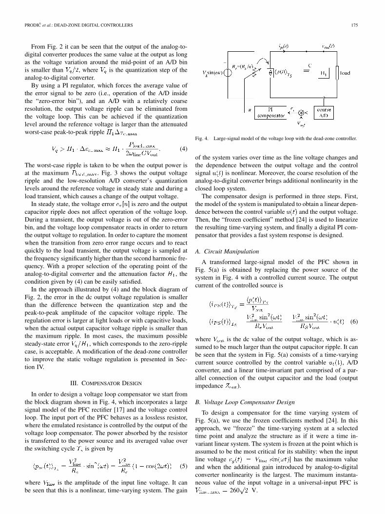
In order to design a voltage loop compensator we start fromthe block diagram shown in Fig. 4, which incorporates a largesignal model of the PFC rectifier [17] and the voltage controlloop. The input port of the PFC behaves as a lossless resistor,where the emulated resistance is controlled by the output of thevoltage loop compensator. The power absorbed by the resistoris transferred to the power source and its averaged value overthe switching cycle is given by
(5)
where is the amplitude of the input line voltage. It canbe seen that this is a nonlinear, time-varying system. The gain
Fig. 4. Large-signal model of the voltage loop with the dead-zone controller.
of the system varies over time as the line voltage changes andthe dependence between the output voltage and the controlsignal is nonlinear. Moreover, the coarse resolution of theanalog-to-digital converter brings additional nonlinearity in theclosed loop system.
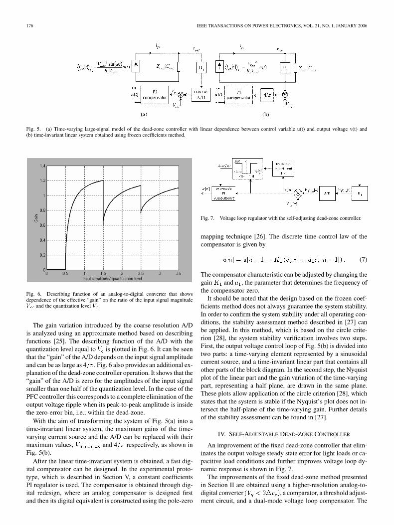
The compensator design is performed in three steps. First,the model of the system is manipulated to obtain a linear depen-dence between the control variable and the output voltage.Then, the “frozen coefficient” method [24] is used to linearizethe resulting time-varying system, and finally a digital PI com-pensator that provides a fast system response is designed.
A. Circuit Manipulation
A transformed large-signal model of the PFC shown inFig. 5(a) is obtained by replacing the power source of thesystem in Fig. 4 with a controlled current source. The outputcurrent of the controlled source is
(6)
where is the dc value of the output voltage, which is as-sumed to be much larger than the output capacitor ripple. It canbe seen that the system in Fig. 5(a) consists of a time-varyingcurrent source controlled by the control variable , A/Dconverter, and a linear time-invariant part comprised of a par-allel connection of the output capacitor and the load (outputimpedance ).
B. Voltage Loop Compensator Design
To design a compensator for the time varying system ofFig. 5(a), we use the frozen coefficients method [24]. In thisapproach, we “freeze” the time-varying system at a selectedtime point and analyze the structure as if it were a time in-variant linear system. The system is frozen at the point which isassumed to be the most critical for its stability: when the inputline voltage has the maximum valueand when the additional gain introduced by analog-to-digitalconverter nonlinearity is the largest. The maximum instanta-neous value of the input voltage in a universal-input PFC is
260 V.
176 IEEE TRANSACTIONS ON POWER ELECTRONICS, VOL. 21, NO. 1, JANUARY 2006
Fig. 5. (a) Time-varying large-signal model of the dead-zone controller with linear dependence between control variable u(t) and output voltage v(t) and(b) time-invariant linear system obtained using frozen coefficients method.
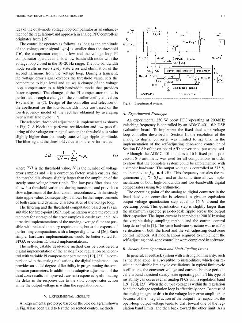
Fig. 6. Describing function of an analog-to-digital converter that showsdependence of the effective “gain” on the ratio of the input signal magnitudeV and the quantization level V .
The gain variation introduced by the coarse resolution A/Dis analyzed using an approximate method based on describingfunctions [25]. The describing function of the A/D with thequantization level equal to is plotted in Fig. 6. It can be seenthat the “gain” of the A/D depends on the input signal amplitudeand can be as large as 4 . Fig. 6 also provides an additional ex-planation of the dead-zone controller operation. It shows that the“gain” of the A/D is zero for the amplitudes of the input signalsmaller than one half of the quantization level. In the case of thePFC controller this corresponds to a complete elimination of theoutput voltage ripple when its peak-to-peak amplitude is insidethe zero-error bin, i.e., within the dead-zone.
With the aim of transforming the system of Fig. 5(a) into atime-invariant linear system, the maximum gains of the time-varying current source and the A/D can be replaced with theirmaximum values, and 4 respectively, as shown inFig. 5(b).
After the linear time-invariant system is obtained, a fast dig-ital compensator can be designed. In the experimental proto-type, which is described in Section V, a constant coefficientsPI regulator is used. The compensator is obtained through dig-ital redesign, where an analog compensator is designed firstand then its digital equivalent is constructed using the pole-zero
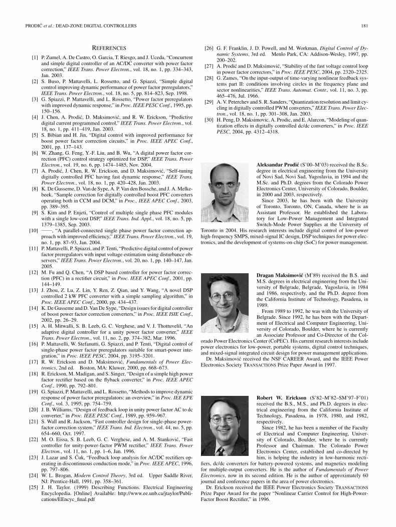
Fig. 7. Voltage loop regulator with the self-adjusting dead-zone controller.
mapping technique [26]. The discrete time control law of thecompensator is given by
(7)
The compensator characteristic can be adjusted by changing thegain and , the parameter that determines the frequency ofthe compensator zero.
It should be noted that the design based on the frozen coef-ficients method does not always guarantee the system stability.In order to confirm the system stability under all operating con-ditions, the stability assessment method described in [27] canbe applied. In this method, which is based on the circle crite-rion [28], the system stability verification involves two steps.First, the output voltage control loop of Fig. 5(b) is divided intotwo parts: a time-varying element represented by a sinusoidalcurrent source, and a time-invariant linear part that contains allother parts of the block diagram. In the second step, the Nyquistplot of the linear part and the gain variation of the time-varyingpart, representing a half plane, are drawn in the same plane.These plots allow application of the circle criterion [28], whichstates that the system is stable if the Nyquist’s plot does not in-tersect the half-plane of the time-varying gain. Further detailsof the stability assessment can be found in [27].
IV. SELF-ADJUSTABLE DEAD-ZONE CONTROLLER
An improvement of the fixed dead-zone controller that elim-inates the output voltage steady state error for light loads or ca-pacitive load conditions and further improves voltage loop dy-namic response is shown in Fig. 7.
The improvements of the fixed dead-zone method presentedin Section II are obtained using a higher-resolution analog-to-digital converter , a comparator, a threshold adjust-ment circuit, and a dual-mode voltage loop compensator. The
PRODIC et al.: DEAD-ZONE DIGITAL CONTROLLERS 177
idea of the dual-mode voltage loop compensator as an enhance-ment of the regulation-band approach in analog PFC controllersoriginates from [19].
The controller operates as follows: as long as the amplitudeof the voltage error signal is smaller than the threshold
, the comparator output is low and the voltage loop PIcompensator operates in a slow low-bandwidth mode with thevoltage loop closed in the 10–20 Hz range. The low-bandwidthmode results in zero steady state error and elimination of thesecond harmonic from the voltage loop. During a transient,the voltage error signal exceeds the threshold value, sets thecomparator to high level and causes a change of the voltageloop compensator to a high-bandwidth mode that providesfaster response. The change of the PI compensator mode isperformed through a change of the controller coefficient values
, and in (7). Design of the controller and selection ofthe coefficient for the low-bandwidth mode are based on thelow-frequency model of the rectifier obtained by averagingover a half line cycle [17].
The adaptive threshold adjustment is implemented as shownin Fig. 7. A block that performs rectification and low-pass fil-tering of the voltage error signal sets up the threshold to a valueslightly higher than the steady-state voltage ripple amplitude.The filtering and the threshold calculation are performed as
(8)
where is the threshold value, is the number of voltageerror samples and is a correction factor, which ensures thatthe threshold is always slightly larger than the amplitude of thesteady state voltage error ripple. The low-pass filter does notallow fast threshold variations during transients, and provides aslow adjustment of the dead-zone in accordance with the steadystate ripple value. Consequently, it allows further improvementsof both static and dynamic characteristics of the voltage loop.
The filtering and the threshold computation based on (8) aresuitable for fixed-point DSP implementation where the requiredmemory for storage of the error samples is easily available. Al-ternative implementations of the moving-average filter are pos-sible with reduced memory requirements, but at the expense ofperforming computations with a longer digital word [26]. Suchsimpler hardware implementations would be better suited forFPGA or custom IC based implementations.
The self-adjustable dead-zone method can be considered adigital implementation of the analog fixed regulation band con-trol with variable PI compensator parameters [19], [23]. In com-parison with the analog realizations, the digital implementationprovides an added degree of flexibility in programming the com-pensator parameters. In addition, the adaptive adjustment of thedead zone results in improved transient responses by eliminatingthe delay in the response due to the slow compensator actionwhile the output voltage is within the regulation band.
V. EXPERIMENTAL RESULTS
An experimental prototype based on the block diagram shownin Fig. 8 has been used to test the presented control methods.
Fig. 8. Experimental system.
A. Experimental Prototype
An experimental 250 W boost PFC operating at 200-kHzswitching frequency is controlled by an ADMC-401 16-b DSPevaluation board. To implement the fixed dead-zone voltageloop controller described in Section II, the resolution of theanalog to digital converter was limited to six bits. In theimplementation of the self-adjusting dead-zone controller ofSection IV, 8 b of the on-board A/D converter output were used.
Although the ADMC-401 includes a 16-b fixed-point pro-cessor, 8-b arithmetic was used for all computations in orderto show that the complete system could be implemented witha simpler hardware. The output voltage is controlled at 375 V,and sampled at 4 kHz. This frequency satisfies the re-quirement , and at the same time allows imple-mentation of both high-bandwidth and low-bandwidth digitalcompensators using 8-b arithmetic.
The operating point of the analog to digital converter in thefixed dead-zone controller is selected to give an equivalentoutput voltage quantization step equal to 15 V around theoperating point. This quantization step is slightly larger thanthe maximum expected peak-to-peak ripple across the outputfilter capacitor. The input current is sampled at 200 kHz usingthe variable-delay sampling method and the current controlloop described in [7]. The same hardware structure was used forverification of both the fixed and the self-adjusting dead-zonecontrol methods. All modifications required to implement theself-adjusting dead-zone controller were completed in software.
B. Steady-State Operation and Limit-Cycling Issues
In general, a feedback system with a strong nonlinearity, suchas the dead zone, is susceptible to instabilities, which can re-sult in undesirable limit cycle oscillations. In typical limit cycleoscillations, the converter voltage and currents bounce periodi-cally around a desired steady-state operating point. This type ofinstability can occur even in analog PFCs with a regulation band[19], [20], [23]. When the output voltage is within the regulationband, the voltage regulation loop is effectively open. Because ofthe analog integrator drift in the voltage-loop error amplifier, orbecause of the integral action of the output filter capacitor, theopen-loop output voltage tends to drift toward one of the reg-ulation band limits, and then back toward the other limit. As a

178 IEEE TRANSACTIONS ON POWER ELECTRONICS, VOL. 21, NO. 1, JANUARY 2006
result, the output voltage and the amplitude of the input currentmay bounce periodically around the desired steady-state values.
In this section, we examine steady-state operation andpossible limit-cycle oscillations in the proposed digital dead-zone controllers. Experimental results are used to illustrate thediscussion.
Consider a PFC with a resistive load R and the fixeddead-zone controller of Section II. In steady state, referringto Fig. 4, the command is constant and, neglectinglosses, the output power averaged over one half line cycle is
. The steady-state solution forthe dc output voltage can be found from
(9)
Because of the quantization of the command , the finite res-olution of the A/D converters for sensing the input voltageand the input current , as well as the finite resolution of theDPWM, the power is also quantized. Let be the powerquantization level, i.e., the effective least significant bit (LSB)value of the average power delivered to the output. From (9)we can find the quantization step in the output voltagethat corresponds to the power quantization level
(10)
(11)
Similar to the static no-limit-cycling condition formulated in[29], [30] for digitally controlled dc/dc converters, the staticno-limit-cycling condition for the PFC with the fixed dead-zonecontroller can be formulated in terms of the output voltage quan-tization step and the quantization step of the outputvoltage A/D converter
(12)
Notice that (12) is a necessary condition for existence of a stablesteady-state solution. If the condition (12) is not satisfied, theoutput voltage will bounce around the desired steady-statevalue. Combining (11) and (12), we have the static no-limit-cy-cling condition
(13)
which implies that the effective resolution in the power com-mand must be better than the resolution of the voltage A/D con-verter. This condition is comparable to the static no-limit-cy-cling condition for digitally controlled dc/dc converters [29],[30], which states that the effective DPWM resolution (in termsof the output voltage) must be better than the resolution of theA/D converter. For a given input line voltage, in (13) dependson the hardware realization, and is a constant. Hence, the con-dition (13) is more difficult to meet at lower output power.
In our experimental prototype with the fixed dead-time con-troller, we found that the PFC has a stable steady-state opera-tion without limit-cycle oscillations for the output power greaterthan about 50 W, or about 20% of the maximum output power.
Fig. 9. Limit-cycle oscillations in the experimental PFC with the fixeddead-zone controller at a light load (45 W). Time scale is 50 ms/div, Ch.1:v (t), 50 V/div, Ch-2: i (t), 0.2 A/div. The input rms voltage is 110 V.
Fig. 10. Input current and output voltage in steady state operation of the PFCwith the self-adjustable dead-zone controller. The input voltage is V =110 rms, and the output load is 45 W (top) and 75 W (bottom) Ch-1: v (t),50 V/div, Ch-2: i (t) 0.5 A/div.
For example, Fig. 9 shows limit cycle oscillations at the outputpower of 45 W.
For analog PFC controller with a regulation band, a PI com-pensator with changing parameters (slow inside the regulationband, and fast outside the regulation band) has been proposed asa solution to the limit-cycle oscillation problem [19]. As notedin Section IV, the self-adjustable dead-zone controller is a dig-ital implementation of this approach.
Fig. 10 shows stable steady-state operation of the PFC withthe adjustable dead-zone controller at 45 W and at 75 W. Nolimit cycle oscillations are observed. Fig. 11 shows an expandedview of the steady-state input voltage and ac line current, demon-strating low harmonic distortion and high power factor of the ex-perimental PFC rectifier with adjustable dead-zone control.

PRODIC et al.: DEAD-ZONE DIGITAL CONTROLLERS 179
Fig. 11. Input current and rectified input voltage in steady-state operation ofthe PFC with the self-adjustable dead-zone controller. The rms value of the inputvoltage is 110 V, the output voltage is regulated at 375 V and the output loadis 100 W. The measured power factor is 0.997. Ch-1: v (t), 50 V/div, Ch-2:i (t) 1 A/div.
Fig. 12. Load transient response of the experimental PFC system with aconventional, slow controller for 100 W–50 W and 50 W–100 W load changesfor V = 110 V. Time scale 200 ms/div, Ch-1: v (t), 60 V/div, Ch-2:i (t), 1 A/div.
C. Load Transient Responses
As a reference, Fig. 12 shows 100 W–50 W–100 W load tran-sient responses of the PFC with a conventional, slow voltageloop controller. This controller is the same as the low-band-width controller of the self-adjustable dead-zone method. Largeovershoots and dips of the output voltage can be observed, withsettling times that extend over a number of line periods. Theovershoots cause additional voltage stresses on the components,while the voltage dips could cause a loss of regulation at highinput line voltage, and increased current stresses on a down-stream converter. Attempting to increase the bandwidth of thevoltage loop without eliminating even harmonics of the line fre-quency from the loop results in much higher harmonic distor-tion, as shown in [7] and [18].
Figs. 13–15 show load transient responses of the fixed andself-adjustable dead-zone controllers for the 100 W–150 W–100 W output load change. Because of the increased voltageripple at heavier loads, the output voltage regulation in the fixeddead-zone controller is improved, and since the output poweris relatively high, no limit cycle oscillations are observed. Bothmethods result in very similar load transient responses. Com-pared to the conventional low-bandwidth design, the responsesare much faster, and the voltage overshoots and dips are signif-icantly smaller. Fig. 15 shows that similar transient responsesare obtained at high line voltage, even though no feed-forward
Fig. 13. Load transient response for 100 W–150 W–100 W output loadchanges in the experimental PFC with the fixed dead-zone controller (top) andthe self-adjustable dead-zone controller (bottom). Time scale 50 ms/div, Ch-1:v (t), 50 V/div, Ch-2: load transient, Ch-4: i (t), 0.5 A/div. The input rmsvoltage is 110 V.
Fig. 14. Details of the load transient responses for 100 W–150 W–100 Woutput load changes in the experimental PFC with the adjustable dead-zonecontroller. Top: light-to-heavy load transient. Bottom: heavy-to-light loadtransient. Time scale is 20 ms/div, Ch-1: v (t), 10 V/div (ac-coupling), Ch-2:i (t),1 A/div. The input rms voltage is 110 V.
compensation of the input voltage was implemented in the ex-perimental PFC with the self-adjustable dead-zone controller.

180 IEEE TRANSACTIONS ON POWER ELECTRONICS, VOL. 21, NO. 1, JANUARY 2006
Fig. 15. Output voltage and input current during load transients between150 W and 250 W for the input rms voltage of 110 V (top) and 220 V (bottom).The time scale is 50 ms/div, Ch-1: v (t), 10 V/div (ac-coupling), Ch-2:i (t), 2 A/div.
Fig. 16. Output voltage and input current during a 30–60 W load transientin the experimental PFC with the fixed dead-zone controller (top), and theself-adjustable dead-zone controller (bottom). The time scale is 100 ms/div,Ch1: v (t), 50 V/div, Ch-2: i (t), 0.5 A/div.
Fig. 16 shows light-load transients (30 to 60 W). For the fixeddead-zone method, limit-cycle oscillations can be observed for
the light load case (30 W). When the output power is increasedto 60 W, the PFC with the fixed dead-zone controller exhibitsa stable steady-state operation. No limit-cycle oscillations areobserved when the self-adjustable dead-zone controller is ap-plied. These observations are consistent with the discussion inSection V-B.
VI. CONCLUSION
This paper describes a dead-zone control method for im-provement of voltage loop dynamic responses in digitally con-trolled low-harmonic rectifiers [i.e., power factor correctors(PFC)]. Implementation of the dead-zone controller is basedon a simple modification of the analog-to-digital convertercharacteristic and does not require any additional hardwareor processing. The dead-zone is the range of output voltagesthat produces a zero error at the output of the A/D converter.By selecting the A/D resolution, i.e., its quantization step,around the reference, the dead-zone is selected to be largerthan the expected output voltage ripple. In steady-state, theoutput voltage error is zero and the second harmonic does notaffect operation of the voltage loop. In transients, a fast voltageloop can be designed to quickly bring the output voltage backto regulation, without increasing distortion of the input linecurrent.
A method for fast voltage loop compensator design isalso shown. It is based on a transformation of the nonlineartime-varying model of the fast voltage loop into a lineartime-invariant system using a describing function model forthe voltage A/D converter, and the frozen coefficient methodto replace the time-varying part of the system with a linear,time-invariant model. The system stability can be verified usinga method based on the circle criterion.
Two versions of the dead-zone method are presented: a fixeddead-zone controller and a self-adjusting dead-zone controller.In the fixed dead-zone method, the zero error range has aconstant value, designed for the maximum expected outputvoltage ripple. In the self-adjustable method, the dead zoneis adjusted to match the actual output voltage ripple. Withchanges in the control software and a relatively small increasein processing, the self-adjusting dead-zone controller offersimproved static voltage regulation and improved steady-stateoperation without limit cycle oscillations. Both dead-zonecontrollers offer much faster voltage transient responses andsignificantly reduced voltage overshoots and dips compared tostandard, low-bandwidth voltage controllers in PFC systems.
Experimental results obtained on a DSP controlled 250-Wboost PFC operating at 200-KHz switching frequency show anorder of magnitude faster load transient responses with the dead-zone controllers compared to the responses with a conventionallow-bandwidth controller.
Advantages of the proposed method include: smaller outputvoltage variations, a potential for less conservative designs ofthe PFC and downstream dc/dc converters, and simpler con-troller implementation compared to alternative methods for im-provement of voltage-loop dynamic responses in digitally con-trolled PFC systems.
PRODIC et al.: DEAD-ZONE DIGITAL CONTROLLERS 181
REFERENCES
[1] P. Zumel, A. De Castro, O. Garcia, T. Riesgo, and J. Uceda, “Concurrentand simple digital controller of an AC/DC converter with power factorcorrection,” IEEE Trans. Power Electron., vol. 18, no. 1, pp. 334–343,Jan. 2003.
[2] S. Buso, P. Mattavelli, L. Rossetto, and G. Spiazzi, “Simple digitalcontrol improving dynamic performance of power factor preregulators,”IEEE Trans. Power Electron., vol. 18, no. 5, pp. 814–823, Sep. 1998.
[3] G. Spiazzi, P. Mattavelli, and L. Rossetto, “Power factor preregulatorswith improved dynamic response,” in Proc. IEEE PESC Conf., 1995, pp.150–156.
[4] J. Chen, A. Prodic, D. Maksimovic, and R. W. Erickson, “Predictivedigital current programmed control,” IEEE Trans. Power Electron., vol.18, no. 1, pp. 411–419, Jan. 2003.
[5] S. Bibian and H. Jin, “Digital control with improved performance forboost power factor correction circuits,” in Proc. IEEE APEC Conf.,2001, pp. 137–143.
[6] W. Zhang, G. Feng, Y.-F. Liu, and B. Wu, “A digital power factor cor-rection (PFC) control strategy optimized for DSP,” IEEE Trans. PowerElectron., vol. 19, no. 6, pp. 1474–1485, Nov. 2004.
[7] A. Prodic, J. Chen, R. W. Erickson, and D. Maksimovic, “Self-tuningdigitally controlled PFC having fast dynamic response,” IEEE Trans.Power Electron., vol. 18, no. 1, pp. 420–428, Jan. 2003.
[8] K. De Gusseme, D. Van de Sype, A. P. Van den Bossche, and J. A. Melke-beek, “Sample correction for digitally controlled boost PFC convertersoperating both in CCM and DCM,” in Proc., IEEE APEC Conf., 2003,pp. 389–395.
[9] S. Kim and P. Enjeti, “Control of multiple single phase PFC moduleswith a single low-cost DSP,” IEEE Trans. Ind. Appl., vol. 18, no. 5, pp.1379–1385, Sep. 2003.
[10] , “A parallel-connected single phase power factor correction ap-proach with improved efficiency,” IEEE Trans. Power Electron., vol. 19,no. 1, pp. 87–93, Jan. 2004.
[11] P. Mattavelli, P. Spiazzi, and P. Tenti, “Predictive digital control of powerfactor preregulators with input voltage estimation using disturbance ob-servers,” IEEE Trans. Power Electron., vol. 20, no. 1, pp. 140–147, Jan.2005.
[12] M. Fu and Q. Chen, “A DSP based controller for power factor correc-tion (PFC) in a rectifier circuit,” in Proc. IEEE APEC Conf., 2001, pp.144–149.
[13] J. Zhou, Z. Lu, Z. Lin, Y. Ren, Z. Qian, and Y. Wang, “A novel DSPcontrolled 2 kW PFC converter with a simple sampling algorithm,” inProc. IEEE APEC Conf., 2000, pp. 434–437.
[14] K. De Gusseme and D. Van De Sype, “Design issues for digital controllerof boost power factor correction converters,” in Proc. IEEE ISIE Conf.,2002, pp. 26–29.
[15] A. H. Mitwalli, S. B. Leeb, G. C. Verghese, and V. J. Thottuvelil, “Anadaptive digital controller for a unity power factor converter,” IEEETrans. Power Electron., vol. 11, no. 2, pp. 374–382, Mar. 1996.
[16] P. Mattavelli, W. Stefanutti, G. Spiazzi, and P. Tenti, “Digital control ofsingle-phase power factor preregulators suitable for smart-power inte-gration,” in Proc. IEEE PESC, 2004, pp. 3195–3201.
[17] R. W. Erickson and D. Maksimovic, Fundamentals of Power Elec-tronics, 2nd ed. Boston, MA: Kluwer, 2000, pp. 668–673.
[18] R. Erickson, M. Madigan, and S. Singer, “Design of a simple high powerfactor rectifier based on the flyback converter,” in Proc. IEEE APECConf., 1990, pp. 792–801.
[19] G. Spiazzi, P. Mattavelli, and L. Rossetto, “Methods to improve dynamicresponse of power factor preregulators: an overview,” in Proc. IEE EPEConf., vol. 3, 1995, pp. 754–759.
[20] J. B. Williams, “Design of feedback loop in unity power factor AC to dcconverter,” in Proc. IEEE PESC Conf., 1989, pp. 959–967.
[21] S. Wall and R. Jackson, “Fast controller design for single-phase power-factor correction system,” IEEE Trans. Ind. Electron., vol. 44, no. 5, pp.654–660, Oct. 1997.
[22] M. O. Eissa, S. B. Leeb, G. C. Verghese, and A. M. Stankovic, “Fastcontroller for unity-power-factor PWM rectifier,” IEEE Trans. PowerElectron., vol. 11, no. 1, pp. 1–6, Jan. 1996.
[23] J. Lazar and S. Cuk, “Feedback loop analysis for AC/DC rectifiers op-erating in discontinuous conduction mode,” in Proc. IEEE APEC, 1996,pp. 797–806.
[24] W. L. Brogan, Modern Control Theory, 3rd ed. Upper Saddle River,NJ: Prentice-Hall, 1991, pp. 358–361.
[25] J. H. Taylor. (1999) Describing Functions. Electrical EngineeringEncyclopedia. [Online] Available: http://www.ee.unb.ca/jtaylor/Publi-cations/EEncyc_final.pdf
[26] G. F. Franklin, J. D. Powell, and M. Workman, Digital Control of Dy-namic Systems, 3rd ed. Menlo Park, CA: Addison-Wesley, 1997, pp.200–202.
[27] A. Prodic and D. Maksimovic, “Stability of the fast voltage control loopin power factor correctors,” in Proc. IEEE PESC, 2004, pp. 2320–2325.
[28] G. Zames, “On the input-output of time-varying nonlinear feedback sys-tems part II: conditions involving circles in the frequency plane andsector nonlinearities,” IEEE Trans. Automat. Contr., vol. 11, no. 3, pp.465–476, Jul. 1966.
[29] A. V. Peterchev and S. R. Sanders, “Quantization resolution and limit cy-cling in digitally controlled PWM converters,” IEEE Trans. Power Elec-tron., vol. 18, no. 1, pp. 301–308, Jan. 2003.
[30] H. Peng, D. Maksimovic, A. Prodic, and E. Alarcon, “Modeling of quan-tization effects in digitally controlled dc/dc converters,” in Proc. IEEEPESC, 2004, pp. 4312–4318.
Aleksandar Prodic (S’00–M’03) received the B.Sc.degree in electrical engineering from the Universityof Novi Sad, Novi Sad, Yugoslavia, in 1994 and theM.Sc. and Ph.D. degrees from the Colorado PowerElectronics Center, University of Colorado, Boulder,in 2000 and 2003, respectively.
Since 2003, he has been with the Universityof Toronto, Toronto, ON, Canada, where he is anAssistant Professor. He established the Labora-tory for Low-Power Management and IntegratedSwitch-Mode Power Supplies at the University of
Toronto in 2004. His research interests include digital control of low-powerhigh-frequency SMPS, mixed-signal IC design, DSP techniques for power elec-tronics, and the development of systems-on-chip (SoC) for power management.
Dragan Maksimovic (M’89) received the B.S. andM.S. degrees in electrical engineering from the Uni-versity of Belgrade, Belgrade, Yugoslavia, in 1984and 1986, respectively, and the Ph.D. degree fromthe California Institute of Technology, Pasadena, in1989.
From 1989 to 1992, he was with the University ofBelgrade. Since 1992, he has been with the Depart-ment of Electrical and Computer Engineering, Uni-versity of Colorado, Boulder, where he is currentlyan Associate Professor and Co-Director of the Col-
orado Power Electronics Center (CoPEC). His current research interests includepower electronics for low-power, portable systems, digital control techniques,and mixed-signal integrated circuit design for power management applications.
Dr. Maksimovic received the NSF CAREER Award, and the IEEE PowerElectronics Society TRANSACTIONS Prize Paper Award in 1997.
Robert W. Erickson (S’82–M’82–SM’97–F’01)received the B.S., M.S., and Ph.D. degrees in elec-trical engineering from the California Institute ofTechnology, Pasadena, in 1978, 1980, and 1982,respectively.
Since 1982, he has been a member of the Facultyof Electrical and Computer Engineering, Univer-sity of Colorado, Boulder, where he is currentlyProfessor and Chairman. The Colorado PowerElectronics Center, established and co-directed byhim, is helping the industry in low-harmonic recti-
fiers, dc/dc converters for battery-powered systems, and magnetics modelingfor multiple-output converters. He is the author of Fundamentals of PowerElectronics, now in its second edition. He is the author of approximately 60journal and conference papers in the area of power electronics.
Dr. Erickson received the IEEE Power Electronics Society TRANSACTIONS
Prize Paper Award for the paper “Nonlinear Carrier Control for High-Power-Factor Boost Rectifier,” in 1996.