Embed Size (px)
Citation preview
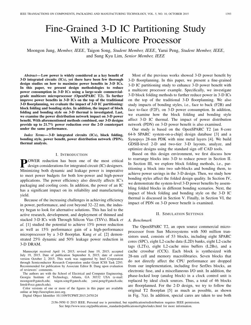
IEEE TRANSACTIONS ON COMPONENTS, PACKAGING AND MANUFACTURING TECHNOLOGY, VOL. 5, NO. 10, OCTOBER 2015 1393
Fine-Grained 3-D IC Partitioning StudyWith a Multicore Processor
Moongon Jung, Member, IEEE, Taigon Song, Student Member, IEEE, Yarui Peng, Student Member, IEEE,and Sung Kyu Lim, Senior Member, IEEE
Abstract— Low power is widely considered as a key benefit of3-D integrated circuits (ICs), yet there have been few thoroughdesign studies on how to maximize power benefits in 3-D ICs.In this paper, we present design methodologies to reducepower consumption in 3-D ICs using a large-scale commercial-grade multicore microprocessor (OpenSPARC T2). To furtherimprove power benefits in 3-D ICs on the top of the traditional3-D floorplanning, we evaluate the impact of 3-D IC partitioning:block folding and bonding styles. In addition, the impact of blockfolding and bonding style on 3-D thermal is investigated. Last,we examine the power distribution network impact on 3-D powerbenefit. With aforementioned methods combined, our 3-D designsprovide up to 21.7% power reduction over the 2-D counterpartunder the same performance.
Index Terms— 3-D integrated circuits (ICs), block folding,bonding style, power benefit, power distribution network (PDN),thermal analysis.
I. INTRODUCTION
POWER reduction has been one of the most criticaldesign considerations for integrated circuit (IC) designers.
Minimizing both dynamic and leakage power is imperativeto meet power budgets for both low-power and high-powerapplications. The power efficiency also directly affects IC’spackaging and cooling costs. In addition, the power of an IChas a significant impact on its reliability and manufacturingyield.
Because of the increasing challenges in achieving efficiencyin power, performance, and cost beyond 32–22 nm, the indus-try began to look for alternative solutions. This has led to theactive research, development, and deployment of thinned andstacked 3-D ICs with Through Silicon Vias (TSVs). Black etal. [1] studied the potential to achieve 15% power reductionas well as 15% performance gain of a high-performancemicroprocessor by a 3-D floorplan. Kang et al. [2] demon-strated 25% dynamic and 50% leakage power reduction in3-D DRAM.
Manuscript received April 14, 2015; revised June 19, 2015; acceptedJuly 19, 2015. Date of publication September 8, 2015; date of currentversion October 2, 2015. This work was supported by Intel Corporationthrough Semiconductor Research Corporation under Grant ICSS Task 2293.Recommended for publication by Associate Editor B. Dang upon evaluationof reviewers’ comments.
The authors are with the School of Electrical and Computer Engineering,Georgia Institute of Technology, Atlanta, GA 30332 USA (e-mail:[email protected]; [email protected]; [email protected];[email protected]).
Color versions of one or more of the figures in this paper are availableonline at http://ieeexplore.ieee.org.
Digital Object Identifier 10.1109/TCPMT.2015.2470124
Most of the previous works showed 3-D power benefit by3-D floorplanning. In this paper, we present a fine-grained3-D IC partitioning study to enhance 3-D power benefit witha multicore processor example. Specifically, we investigate3-D block folding methods to further reduce power in 3-D ICson the top of the traditional 3-D floorplanning. We alsostudy impacts of bonding styles, i.e., face to back (F2B) andface to-face (F2F), on 3-D power consumption. In addition,we examine how the block folding and bonding styleaffect 3-D IC thermal. The impact of power distributionnetwork (PDN) on 3-D power benefit is also examined.
Our study is based on the OpenSPARC T2 [an 8-core64-b SPARC system-on-a-chip] design database [3] and aSynopsys 28-nm PDK with nine metal layers [4]. We buildGDSII-level 2-D and two-tier 3-D layouts, analyze, andoptimize designs using the standard sign off CAD tools.
Based on this design environment, we first discuss howto rearrange blocks into 3-D to reduce power in Section II.In Section III, we explore block folding methods, i.e., par-titioning a block into two sub-blocks and bonding them, toachieve power savings in the 3-D design. Then, we study howbonding styles affect the folded design quality. In Section IV,we demonstrate the system-level 3-D power benefits by assem-bling folded blocks in different bonding scenarios. Next, theimpact of block folding and bonding style on the 3-D ICthermal is discussed in Section V. Finally, in Section VI, theimpact of PDN on 3-D power benefit is examined.
II. SIMULATION SETTINGS
A. Benchmark
The OpenSPARC T2, an open source commercial micro-processor from Sun Microsystems with 500 million tran-sistors used, consists of 53 blocks, including eight SPARCcores (SPC), eight L2-cache data (L2D) banks, eight L2-cachetags (L2Ts), eight L2-cache miss buffers (L2Bs), and acache crossbar (CCX). Each block is synthesized with28-nm cell and memory macrolibraries. Seven blocks thatdo not directly affect the CPU performance are droppedfrom our implementation, including five SerDes blocks, anelectronic fuse, and a miscellaneous I/O unit. In addition, thephase-locked loop (analog block) in a clock control unit isreplaced by ideal clock sources. Thus, a total of 46 blocksare floorplanned. For the 2-D design, we try to follow theoriginal T2 floorplan [5] as much as possible, as shownin Fig. 7(a). In addition, special cares are taken to use both
2156-3950 © 2015 IEEE. Personal use is permitted, but republication/redistribution requires IEEE permission.See http://www.ieee.org/publications_standards/publications/rights/index.html for more information.
1394 IEEE TRANSACTIONS ON COMPONENTS, PACKAGING AND MANUFACTURING TECHNOLOGY, VOL. 5, NO. 10, OCTOBER 2015
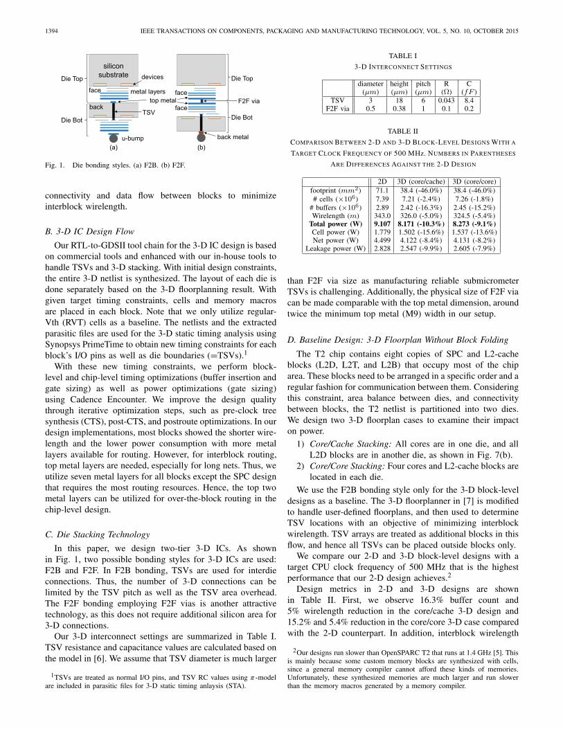
Fig. 1. Die bonding styles. (a) F2B. (b) F2F.
connectivity and data flow between blocks to minimizeinterblock wirelength.
B. 3-D IC Design Flow
Our RTL-to-GDSII tool chain for the 3-D IC design is basedon commercial tools and enhanced with our in-house tools tohandle TSVs and 3-D stacking. With initial design constraints,the entire 3-D netlist is synthesized. The layout of each die isdone separately based on the 3-D floorplanning result. Withgiven target timing constraints, cells and memory macrosare placed in each block. Note that we only utilize regular-Vth (RVT) cells as a baseline. The netlists and the extractedparasitic files are used for the 3-D static timing analysis usingSynopsys PrimeTime to obtain new timing constraints for eachblock’s I/O pins as well as die boundaries (=TSVs).1
With these new timing constraints, we perform block-level and chip-level timing optimizations (buffer insertion andgate sizing) as well as power optimizations (gate sizing)using Cadence Encounter. We improve the design qualitythrough iterative optimization steps, such as pre-clock treesynthesis (CTS), post-CTS, and postroute optimizations. In ourdesign implementations, most blocks showed the shorter wire-length and the lower power consumption with more metallayers available for routing. However, for interblock routing,top metal layers are needed, especially for long nets. Thus, weutilize seven metal layers for all blocks except the SPC designthat requires the most routing resources. Hence, the top twometal layers can be utilized for over-the-block routing in thechip-level design.
C. Die Stacking Technology
In this paper, we design two-tier 3-D ICs. As shownin Fig. 1, two possible bonding styles for 3-D ICs are used:F2B and F2F. In F2B bonding, TSVs are used for interdieconnections. Thus, the number of 3-D connections can belimited by the TSV pitch as well as the TSV area overhead.The F2F bonding employing F2F vias is another attractivetechnology, as this does not require additional silicon area for3-D connections.
Our 3-D interconnect settings are summarized in Table I.TSV resistance and capacitance values are calculated based onthe model in [6]. We assume that TSV diameter is much larger
1TSVs are treated as normal I/O pins, and TSV RC values using π -modelare included in parasitic files for 3-D static timing anlaysis (STA).
TABLE I
3-D INTERCONNECT SETTINGS
TABLE II
COMPARISON BETWEEN 2-D AND 3-D BLOCK-LEVEL DESIGNS WITH A
TARGET CLOCK FREQUENCY OF 500 MHz. NUMBERS IN PARENTHESES
ARE DIFFERENCES AGAINST THE 2-D DESIGN
than F2F via size as manufacturing reliable submicrometerTSVs is challenging. Additionally, the physical size of F2F viacan be made comparable with the top metal dimension, aroundtwice the minimum top metal (M9) width in our setup.
D. Baseline Design: 3-D Floorplan Without Block Folding
The T2 chip contains eight copies of SPC and L2-cacheblocks (L2D, L2T, and L2B) that occupy most of the chiparea. These blocks need to be arranged in a specific order and aregular fashion for communication between them. Consideringthis constraint, area balance between dies, and connectivitybetween blocks, the T2 netlist is partitioned into two dies.We design two 3-D floorplan cases to examine their impacton power.
1) Core/Cache Stacking: All cores are in one die, and allL2D blocks are in another die, as shown in Fig. 7(b).
2) Core/Core Stacking: Four cores and L2-cache blocks arelocated in each die.
We use the F2B bonding style only for the 3-D block-leveldesigns as a baseline. The 3-D floorplanner in [7] is modifiedto handle user-defined floorplans, and then used to determineTSV locations with an objective of minimizing interblockwirelength. TSV arrays are treated as additional blocks in thisflow, and hence all TSVs can be placed outside blocks only.
We compare our 2-D and 3-D block-level designs with atarget CPU clock frequency of 500 MHz that is the highestperformance that our 2-D design achieves.2
Design metrics in 2-D and 3-D designs are shownin Table II. First, we observe 16.3% buffer count and5% wirelength reduction in the core/cache 3-D design and15.2% and 5.4% reduction in the core/core 3-D case comparedwith the 2-D counterpart. In addition, interblock wirelength
2Our designs run slower than OpenSPARC T2 that runs at 1.4 GHz [5]. Thisis mainly because some custom memory blocks are synthesized with cells,since a general memory compiler cannot afford these kinds of memories.Unfortunately, these synthesized memories are much larger and run slowerthan the memory macros generated by a memory compiler.
JUNG et al.: FINE-GRAINED 3-D IC PARTITIONING STUDY WITH A MULTICORE PROCESSOR 1395
reduces by 15.6% (core/cache) and 17.8% (core/core), whichis a direct consequence of 3-D floorplanning.
Second, most importantly, the 3-D designs reduce powerconsumption over the 2-D counterpart by 10.3% (core/cache)and 9.1% (core/core). We see that cell (15.6%) andleakage (9.9%) power reduction are far more than the cellcount decrease (2.4%) in the core/cache 3-D design. This isbecause the 3-D design utilizes more smaller cells than the2-D because of better timing, i.e., more positive timing slackin paths. With the positive slack, cells can be downsized inthe 3-D design if this change still meets the timing constraintduring power optimization stages.
This smaller cell size in the 3-D design also helps reducenet power consumption. The load capacitance of a driving cellis defined as the sum of wire capacitance and the input pincapacitance of the loading side, and hence the net power isdefined as the sum of wire and pin power. Therefore, the wirepower reduction is directly from reduced wirelength, and thepin power decrease is from the smaller cell size as well as thereduced cell count.
Third, the core/cache 3-D stacking case shows 1.2% smallerpower consumption than the core/core case, which is essen-tially a negligible difference. This also indicates that there isnot much room to further reduce power by 3-D floorplans only,since there are not many floorplan options for the T2 designthat contains multiple large same-size blocks that need to beplaced in a specific way.
We choose the core/cache case as a baseline 3-D block-leveldesign as it consumes a little less power than the core/corecase. In addition, this 3-D design will be better in terms of thethermal coupling between dies as SPCs (higher power density)and L2Ds (lower power density) are stacked, while SPCs arestacked in the core/core case.
III. BLOCK FOLDING STRATEGIES
So far, the block-level designs are implemented for both2-D and 3-D designs. Thus, even in the 3-D designs, eachblock is located in the same die. In addition, TSVs are alwaysoutside blocks and used only for interblock connections. In thissection, we examine the impact of block folding, i.e., parti-tioning a single block into two sub-blocks and connect themwith TSVs for intrablock connections, on power consumption.
A. Block Folding Criteria
For the block folding to provide power saving, certaincriteria need to be met. First, the target block is required toconsume a high enough portion of the total system power.Otherwise, the power saving from the block folding couldbe negligible in the system level. Blocks that consume morethan 1% of the total system power are listed in Table III.Note that the total power portion of SPC, L2D, and L2T isthe average of corresponding eight blocks. Thus, SPC, L2D,and L2T are outstanding target blocks. In addition, RTX andCCX consume high power as a single block, and hence couldprovide a nonnegligible power benefit if folded.
Second, the net power portion of the target block needsto be high. If the block is cell and leakage power dominant,the wirelength reduction of the folded block may not reduce
TABLE III
2-D DESIGN CHARACTERISTICS OF FOLDING CANDIDATE BLOCKS.
LONG WIRES ARE DEFINED AS WIRES LONGER THAN
100× STANDARD CELL HEIGHT. CPU CLOCK RUNS
AT 500 MHz AND I/O CLOCK AT 250 MHz
TABLE IV
L2T DIE PARTITIONING SCHEMES
the total power noticeably. Therefore, SPC and CCX areattractive blocks to fold. L2D shows a relatively low net powerportion compared with other blocks as L2D is the memory(and its power) dominated design that contains 512 kB (3216-kB memory macros in our implementation). Third, the targetblock needs to contain many long wires so that wirelengthdecrease, and hence net power reduction in the folded blockcan be maximized. In this paper, we define long wires as wireslonger than the 100× standard cell height. We observe thatSPC, RTX, and CCX have a large number of long wires.
In this paper, we fold five blocks: 1) SPC; 2) CCX; 3) L2D;4) L2T; and 5) RTX. In the following sections III-B and III-C, we discuss the block folding methodologies for SPC andL2T. Each block shows the distinctive folding characteristics.We tried both manual (based on design information such asconnectivity between submodules) and automated (min-cutpartitioner with cut size control) partitioning methods for eachblock folding, and selected a better case.
B. Folding L2T Block
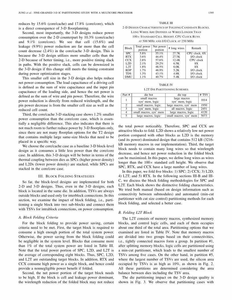
The L2T consists of memory macros, synthesized memoryblocks, and control logic cells, and each of them occupiesabout one third of the total area. Partitioning options that weexamined are listed in Table IV. Note that memory macrosare divided into two groups based on their connectivities,i.e., tightly connected macros form a group. In partition #1,after splitting memory blocks, logic cells are partitioned usinga min-cut partitioner, which leads to the smallest number ofTSVs among five cases. On the other hand, in partition #5,where the largest number of TSVs are used, the silicon areaoccupied by TSVs is as high as 10%, as shown in Fig. 2.All these partitions are determined considering the areabalance between dies including the TSV area.
The die partitioning impact on the 3-D design quality isshown in Fig. 3. We observe that partitioning cases with
1396 IEEE TRANSACTIONS ON COMPONENTS, PACKAGING AND MANUFACTURING TECHNOLOGY, VOL. 5, NO. 10, OCTOBER 2015
Fig. 2. L2T 2-D and 3-D layouts. (a) 2-D design. (b) 3-D design ofpartition #5 in Table IV (#TSV: 5 073). The total TSV area is 10%.
Fig. 3. Impact of L2T die partitioning on wirelength, buffer count, and power.All numbers are normalized to the 2-D.
a larger number of TSVs tend to lose the 3-D power benefit.For example, partition #1 (#TSV: 1014) shows 15.7% powersaving, while partition #5 (#TSV: 5073) achieves only 4.7%power reduction compared with the 2-D. In these cases, thelarge TSV area overhead results in the increase in footprintarea, wirelength, buffer usage, and hence power consumption.However, we cannot generalize that more 3-D connectionsdegrade the 3-D design quality as this highly depends on3-D interconnect elements.
C. Second-Level Folding SPC Block
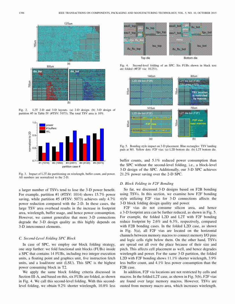
In case of SPC, we employ our block folding strategy,one step further: we fold functional unit blocks (FUBs) insidea SPC that contains 14 FUBs, including two integer executionunits, a floating point and graphics unit, five instruction fetchunits, and a load/store unit (LSU). This SPC is the highestpower consuming block in T2.
We apply the same block folding criteria discussed inSection III-A, and based on this, six FUBs are folded, as shownin Fig. 4. We call this second-level folding. With this second-level folding, we obtain 9.2% shorter wirelength, 10.8% less
Fig. 4. Second-level folding of an SPC. Six FUBs shown in black textare folded (#F2F via: 10 251).
Fig. 5. Bonding style impact on 3-D placement. Blue rectangles: TSV landingpads at M1. Yellow dots: F2F vias. (a) L2D bottom die. (b) L2T bottom die.
buffer counts, and 5.1% reduced power consumption thanthe SPC without the second-level folding, i.e., a block-level3-D design of the SPC. Additionally, our 3-D SPC achieves21.2% power saving over the 2-D SPC.
D. Block Folding in F2F Bonding
So far, we discussed 3-D designs based on F2B bondingusing TSVs. In this section, we examine how F2F bondingstyle utilizing F2F vias for 3-D connections affects the3-D block folding design quality and power.
F2F vias do not consume silicon area, and hencea 3-D footprint area can be further reduced, as shown in Fig. 5.For example, the folded L2D and L2T with F2F bondingreduce footprint by 2.6% and 6.3%, respectively, comparedwith F2B bonding cases. In the folded L2D case, as shownin Fig. 5(a), all F2F vias are located on the horizontalchannels between memory macros to connect memory I/O pinsand logic cells right below them. On the other hand, TSVsare spread out all over the place because of their size andpitch. This affects cell placement as well, and hence degradeswirelength and power. For the same 3-D partition, the foldedL2D with F2F bonding shows 11.1% shorter wirelength, 3.9%less buffer count, and 4.1% less power consumption than theF2B case.
In addition, F2F via locations are not restricted by cells andmacros. In the folded L2T case, as shown in Fig. 5(b), F2F viasare found over large memory macros. However, TSVs areousted from memory macro area, which increases wirelength.
JUNG et al.: FINE-GRAINED 3-D IC PARTITIONING STUDY WITH A MULTICORE PROCESSOR 1397
Fig. 6. Bonding style impact on power in L2T folding. Numbersin parentheses are the number of TSVs/F2F vias.
The five partitioning cases for L2T are implemented in bothF2B and F2F bonding styles. Power comparisons between bothbonding styles are shown in Fig. 6. First, F2F wins over theF2B bonding style in all cases. This is the combined effectof reduced footprint, better 3-D connection points, shorterwirelength, less buffer usage, and better timing. Second,F2F bonding cases show larger power savings over theF2B cases in partition cases with more 3-D connections.In particular, partition #5 that shows the smallest 3-D powerbenefit in F2B now achieves the best power saving with theF2F bonding. Compared with the F2B case, the F2F casereduces power by 16.2%. In this specific case, the 3-D designquality in the F2B bonding is degraded largely by TSV areaoverhead, not by the partition. Third, more 3-D connectionsin the F2F style do not necessarily mean better power saving.Although partitions #3 and #4 show much better power savingthan the F2B cases, these power savings are still less thanpartitions #1 and #2. This emphasizes the importance of diepartitioning again.
IV. FULL-CHIP ASSEMBLY WITH FOLDED BLOCKS
So far, we discussed the impacts of block folding alongwith bonding styles on 3-D power savings. In this section,we integrate all these folded blocks into 3-D T2 full-chip andexamine its impact on the system-level power.
A. 3-D Floorplan With Folded Blocks
Based on the block folding criteria in Section III-A,SPC, CCX, L2D, L2T, and RTX are folded. Unlike otherfour blocks, RTX runs at I/O clock frequency (=250 MHz).In addition, almost all signals to/from RTX are connected withMAC, TDS, and RDP that form a network interface unit (NIU)with RTX. Thus, the impact of RTX folding is limited to theRTX and NIU. In this paper, we implement two 3-D designswith folded blocks: 1) T2 with folded SPCs, CCX, L2Ds, andL2Ts and 2) T2 with all five types of blocks folded.
In each case, we build two designs using either F2B orF2F bonding style. Note that there is a difference in routinglayer usage in folded blocks depending on the bonding style.For the F2B bonding, the die bottom of folded blocks usesup to M7 (TSV landing pad at M1) as other unfolded blocks,while the die top utilizes up to M9 (TSV landing pad at M9).Thus, M8 and M9 can be used for over-the-block routing
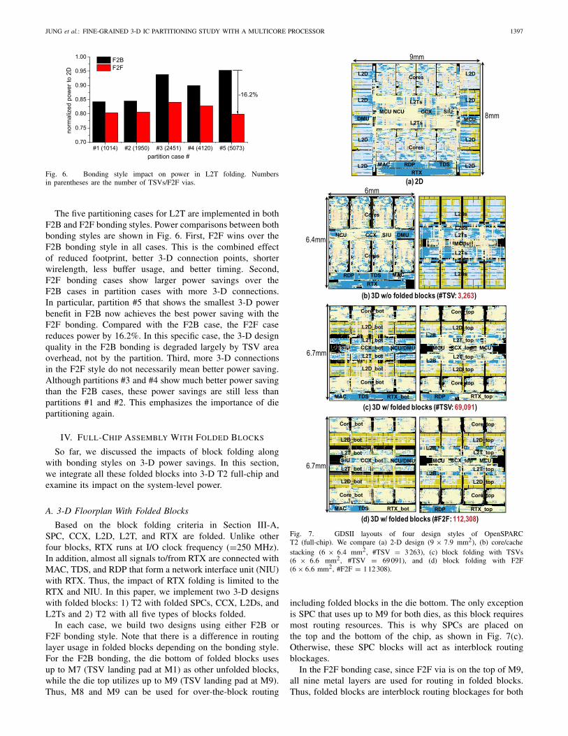
Fig. 7. GDSII layouts of four design styles of OpenSPARCT2 (full-chip). We compare (a) 2-D design (9 × 7.9 mm2), (b) core/cachestacking (6 × 6.4 mm2, #TSV = 3 263), (c) block folding with TSVs(6 × 6.6 mm2, #TSV = 69 091), and (d) block folding with F2F(6 × 6.6 mm2, #F2F = 1 12 308).
including folded blocks in the die bottom. The only exceptionis SPC that uses up to M9 for both dies, as this block requiresmost routing resources. This is why SPCs are placed onthe top and the bottom of the chip, as shown in Fig. 7(c).Otherwise, these SPC blocks will act as interblock routingblockages.
In the F2F bonding case, since F2F via is on the top of M9,all nine metal layers are used for routing in folded blocks.Thus, folded blocks are interblock routing blockages for both
1398 IEEE TRANSACTIONS ON COMPONENTS, PACKAGING AND MANUFACTURING TECHNOLOGY, VOL. 5, NO. 10, OCTOBER 2015
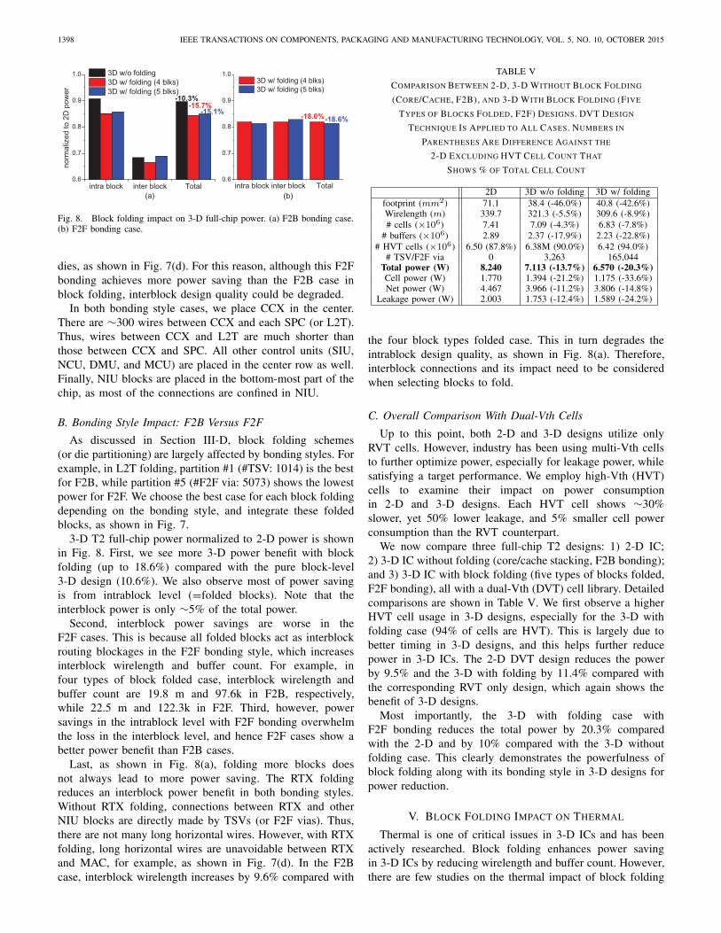
Fig. 8. Block folding impact on 3-D full-chip power. (a) F2B bonding case.(b) F2F bonding case.
dies, as shown in Fig. 7(d). For this reason, although this F2Fbonding achieves more power saving than the F2B case inblock folding, interblock design quality could be degraded.
In both bonding style cases, we place CCX in the center.There are ∼300 wires between CCX and each SPC (or L2T).Thus, wires between CCX and L2T are much shorter thanthose between CCX and SPC. All other control units (SIU,NCU, DMU, and MCU) are placed in the center row as well.Finally, NIU blocks are placed in the bottom-most part of thechip, as most of the connections are confined in NIU.
B. Bonding Style Impact: F2B Versus F2F
As discussed in Section III-D, block folding schemes(or die partitioning) are largely affected by bonding styles. Forexample, in L2T folding, partition #1 (#TSV: 1014) is the bestfor F2B, while partition #5 (#F2F via: 5073) shows the lowestpower for F2F. We choose the best case for each block foldingdepending on the bonding style, and integrate these foldedblocks, as shown in Fig. 7.
3-D T2 full-chip power normalized to 2-D power is shownin Fig. 8. First, we see more 3-D power benefit with blockfolding (up to 18.6%) compared with the pure block-level3-D design (10.6%). We also observe most of power savingis from intrablock level (=folded blocks). Note that theinterblock power is only ∼5% of the total power.
Second, interblock power savings are worse in theF2F cases. This is because all folded blocks act as interblockrouting blockages in the F2F bonding style, which increasesinterblock wirelength and buffer count. For example, infour types of block folded case, interblock wirelength andbuffer count are 19.8 m and 97.6k in F2B, respectively,while 22.5 m and 122.3k in F2F. Third, however, powersavings in the intrablock level with F2F bonding overwhelmthe loss in the interblock level, and hence F2F cases show abetter power benefit than F2B cases.
Last, as shown in Fig. 8(a), folding more blocks doesnot always lead to more power saving. The RTX foldingreduces an interblock power benefit in both bonding styles.Without RTX folding, connections between RTX and otherNIU blocks are directly made by TSVs (or F2F vias). Thus,there are not many long horizontal wires. However, with RTXfolding, long horizontal wires are unavoidable between RTXand MAC, for example, as shown in Fig. 7(d). In the F2Bcase, interblock wirelength increases by 9.6% compared with
TABLE V
COMPARISON BETWEEN 2-D, 3-D WITHOUT BLOCK FOLDING
(CORE/CACHE, F2B), AND 3-D WITH BLOCK FOLDING (FIVE
TYPES OF BLOCKS FOLDED, F2F) DESIGNS. DVT DESIGN
TECHNIQUE IS APPLIED TO ALL CASES. NUMBERS IN
PARENTHESES ARE DIFFERENCE AGAINST THE
2-D EXCLUDING HVT CELL COUNT THAT
SHOWS % OF TOTAL CELL COUNT
the four block types folded case. This in turn degrades theintrablock design quality, as shown in Fig. 8(a). Therefore,interblock connections and its impact need to be consideredwhen selecting blocks to fold.
C. Overall Comparison With Dual-Vth Cells
Up to this point, both 2-D and 3-D designs utilize onlyRVT cells. However, industry has been using multi-Vth cellsto further optimize power, especially for leakage power, whilesatisfying a target performance. We employ high-Vth (HVT)cells to examine their impact on power consumptionin 2-D and 3-D designs. Each HVT cell shows ∼30%slower, yet 50% lower leakage, and 5% smaller cell powerconsumption than the RVT counterpart.
We now compare three full-chip T2 designs: 1) 2-D IC;2) 3-D IC without folding (core/cache stacking, F2B bonding);and 3) 3-D IC with block folding (five types of blocks folded,F2F bonding), all with a dual-Vth (DVT) cell library. Detailedcomparisons are shown in Table V. We first observe a higherHVT cell usage in 3-D designs, especially for the 3-D withfolding case (94% of cells are HVT). This is largely due tobetter timing in 3-D designs, and this helps further reducepower in 3-D ICs. The 2-D DVT design reduces the powerby 9.5% and the 3-D with folding by 11.4% compared withthe corresponding RVT only design, which again shows thebenefit of 3-D designs.
Most importantly, the 3-D with folding case withF2F bonding reduces the total power by 20.3% comparedwith the 2-D and by 10% compared with the 3-D withoutfolding case. This clearly demonstrates the powerfulness ofblock folding along with its bonding style in 3-D designs forpower reduction.
V. BLOCK FOLDING IMPACT ON THERMAL
Thermal is one of critical issues in 3-D ICs and has beenactively researched. Block folding enhances power savingin 3-D ICs by reducing wirelength and buffer count. However,there are few studies on the thermal impact of block folding
JUNG et al.: FINE-GRAINED 3-D IC PARTITIONING STUDY WITH A MULTICORE PROCESSOR 1399
Fig. 9. Thermal structure of F2B and F2F bonding.
and 3-D bonding styles if any. In this section, the thermalimpact of bonding styles, i.e., F2B and F2F, is studied in detail.
A. Thermal Analysis Flow
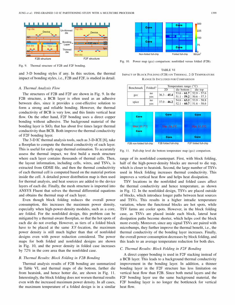
The structures of F2B and F2F are shown in Fig. 9. In theF2B structure, a BCB layer is often used as an adhesivebetween dies, since it provides a cost-effective solution toform a strong and reliable bonding. However, the thermalconductivity of BCB is very low, and this limits vertical heatflow. On the other hand, F2F bonding uses a direct copperbonding without adhesive. The background material of thebonding layer is SiO2 that has about five times larger thermalconductivity than BCB. Both improve the thermal conductivityof F2F bonding layer.
The 3-D IC thermal analysis tools, such as 3-D-ICE [8], takea floorplan to compute the thermal conductivity of each layer.This is useful for early stage thermal estimation. To accuratelyassess the thermal impact, we first build a mesh structurewhere each layer contains thousands of thermal cells. Then,the layout information, including cells, wires, and TSVs, isextracted from GDSII file, and then the thermal conductivityof each thermal cell is computed based on the material portioninside the cell. A detailed power distribution map is then usedfor thermal analysis, and heat sources are added to the devicelayers of each die. Finally, the mesh structure is imported intoANSYS Fluent that solves the thermal differential equationsand obtains the thermal map of each layer.
Even though block folding reduces the overall powerconsumption, this increases the maximum power density,especially when high-power-density modules, such as a core,are folded. For the nonfolded design, this problem can bemitigated by a thermal-aware floorplan, so that the hot spots ofeach die do not overlap. However, as tiers of a folded blockhave to be placed at the same XY -location, the maximumpower density is still much higher than that of nonfoldeddesigns even with power reduction considered. The powermaps for both folded and nonfolded designs are shownin Fig. 10, and the power density in folded case increasesby 72% in the core area than the nonfolded case.
B. Thermal Results: Block Folding in F2B Bonding
Thermal analysis results of F2B bonding are summarizedin Table VI, and thermal maps of die bottom, farther diefrom heatsink, and hence hotter die, are shown in Fig. 11.Interestingly, the block folding does not worsen thermal resultseven with the increased maximum power density. In all cases,the maximum temperature of a folded design is in a similar
Fig. 10. Power map (gcc) comparison: nonfolded versus folded (F2B).
TABLE VI
IMPACT OF BLOCK FOLDING (F2B) ON THERMAL. 2-D TEMPERATURE
RANGE IS INCLUDED FOR COMPARISON
Fig. 11. Full-chip level die bottom temperature map (gcc) comparison.
range of its nonfolded counterpart. First, with block folding,half of the high-power-density blocks are moved to die top,which is closer to heatsink. Second, the large number of TSVsused in block folding increases thermal conductivity. Thisimproves a vertical heat flow and helps heat dissipation.
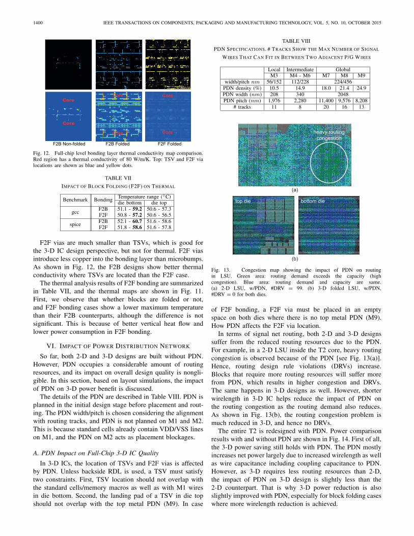
TSV locations in the nonfolded and folded cases affectthe thermal conductivity and hence temperature, as shownin Fig. 12. In the nonfolded design, TSVs are placed outsideof blocks, which introduce longer paths between heat sourcesand TSVs. This results in a higher intradie temperaturevariation, where the functional blocks are hot spots, whileTSV farms are cooler spots. However, in the block foldingcase, as TSVs are placed inside each block, lateral heatdissipation paths become shorter, which helps cool the blockmore evenly. Moreover, since any signal TSVs are paired withmicrobumps, they further improve the thermal benefit, i.e., thethermal conductivity of the bonding layer increases. Finally,the overall power consumption decreases by block folding, andthis leads to an average temperature reduction for both dies.
C. Thermal Results: Block Folding in F2F Bonding
A direct copper bonding is used in F2F stacking instead ofa BCB layer. This leads to a background thermal conductivityimprovement in the bonding layer. In addition, a thinnerbonding layer in the F2F structure has less limitation onvertical heat flow than F2B. Since both metal layers and theF2F bonding layer use the same background material, theF2F bonding layer is no longer the bottleneck for verticalheat flow.
1400 IEEE TRANSACTIONS ON COMPONENTS, PACKAGING AND MANUFACTURING TECHNOLOGY, VOL. 5, NO. 10, OCTOBER 2015
Fig. 12. Full-chip level bonding layer thermal conductivity map comparison.Red region has a thermal conductivity of 80 W/m/K. Top: TSV and F2F vialocations are shown as blue and yellow dots.
TABLE VII
IMPACT OF BLOCK FOLDING (F2F) ON THERMAL
F2F vias are much smaller than TSVs, which is good forthe 3-D IC design perspective, but not for thermal. F2F viasintroduce less copper into the bonding layer than microbumps.As shown in Fig. 12, the F2B designs show better thermalconductivity where TSVs are located than the F2F case.
The thermal analysis results of F2F bonding are summarizedin Table VII, and the thermal maps are shown in Fig. 11.First, we observe that whether blocks are folded or not,and F2F bonding cases show a lower maximum temperaturethan their F2B counterparts, although the difference is notsignificant. This is because of better vertical heat flow andlower power consumption in F2F bonding.
VI. IMPACT OF POWER DISTRIBUTION NETWORK
So far, both 2-D and 3-D designs are built without PDN.However, PDN occupies a considerable amount of routingresources, and its impact on overall design quality is nongli-gible. In this section, based on layout simulations, the impactof PDN on 3-D power benefit is discussed.
The details of the PDN are described in Table VIII. PDN isplanned in the initial design stage before placement and rout-ing. The PDN width/pitch is chosen considering the alignmentwith routing tracks, and PDN is not planned on M1 and M2.This is because standard cells already contain VDD/VSS lineson M1, and the PDN on M2 acts as placement blockages.
A. PDN Impact on Full-Chip 3-D IC Quality
In 3-D ICs, the location of TSVs and F2F vias is affectedby PDN. Unless backside RDL is used, a TSV must satisfytwo constraints. First, TSV location should not overlap withthe standard cells/memory macros as well as with M1 wiresin die bottom. Second, the landing pad of a TSV in die topshould not overlap with the top metal PDN (M9). In case
TABLE VIII
PDN SPECIFICATIONS. # TRACKS SHOW THE MAX NUMBER OF SIGNAL
WIRES THAT CAN FIT IN BETWEEN TWO ADJACENT P/G WIRES
Fig. 13. Congestion map showing the impact of PDN on routingin LSU. Green area: routing demand exceeds the capacity (highcongestion). Blue area: routing demand and capacity are same.(a) 2-D LSU, w/PDN, #DRV = 99. (b) 3-D folded LSU, w/PDN,#DRV = 0 for both dies.
of F2F bonding, a F2F via must be placed in an emptyspace on both dies where there is no top metal PDN (M9).How PDN affects the F2F via location.
In terms of signal net routing, both 2-D and 3-D designssuffer from the reduced routing resources due to the PDN.For example, in a 2-D LSU inside the T2 core, heavy routingcongestion is observed because of the PDN [see Fig. 13(a)].Hence, routing design rule violations (DRVs) increase.Blocks that require more routing resources will suffer morefrom PDN, which results in higher congestion and DRVs.The same happens in 3-D designs as well. However, shorterwirelength in 3-D IC helps reduce the impact of PDN onthe routing congestion as the routing demand also reduces.As shown in Fig. 13(b), the routing congestion problem ismuch reduced in 3-D, and hence no DRVs.
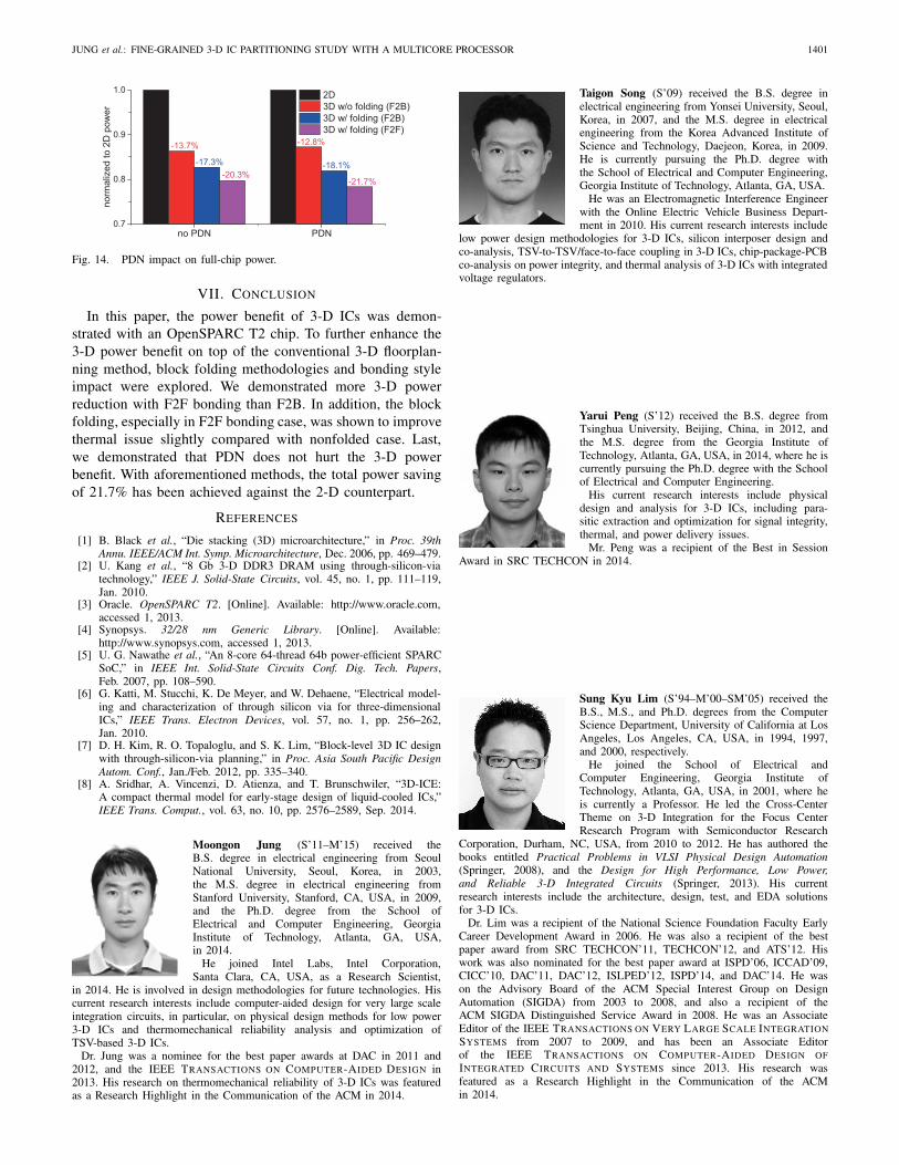
The entire T2 is redesigned with PDN. Power comparisonresults with and without PDN are shown in Fig. 14. First of all,the 3-D power saving still holds with PDN. The PDN mostlyincreases net power largely due to increased wirelength as wellas wire capacitance including coupling capacitance to PDN.However, as 3-D requires less routing resources than 2-D,the impact of PDN on 3-D design is slightly less than the2-D counterpart. That is why 3-D power reduction is alsoslightly improved with PDN, especially for block folding caseswhere more wirelength reduction is achieved.
JUNG et al.: FINE-GRAINED 3-D IC PARTITIONING STUDY WITH A MULTICORE PROCESSOR 1401
Fig. 14. PDN impact on full-chip power.
VII. CONCLUSION
In this paper, the power benefit of 3-D ICs was demon-strated with an OpenSPARC T2 chip. To further enhance the3-D power benefit on top of the conventional 3-D floorplan-ning method, block folding methodologies and bonding styleimpact were explored. We demonstrated more 3-D powerreduction with F2F bonding than F2B. In addition, the blockfolding, especially in F2F bonding case, was shown to improvethermal issue slightly compared with nonfolded case. Last,we demonstrated that PDN does not hurt the 3-D powerbenefit. With aforementioned methods, the total power savingof 21.7% has been achieved against the 2-D counterpart.
REFERENCES
[1] B. Black et al., “Die stacking (3D) microarchitecture,” in Proc. 39thAnnu. IEEE/ACM Int. Symp. Microarchitecture, Dec. 2006, pp. 469–479.
[2] U. Kang et al., “8 Gb 3-D DDR3 DRAM using through-silicon-viatechnology,” IEEE J. Solid-State Circuits, vol. 45, no. 1, pp. 111–119,Jan. 2010.
[3] Oracle. OpenSPARC T2. [Online]. Available: http://www.oracle.com,accessed 1, 2013.
[4] Synopsys. 32/28 nm Generic Library. [Online]. Available:http://www.synopsys.com, accessed 1, 2013.
[5] U. G. Nawathe et al., “An 8-core 64-thread 64b power-efficient SPARCSoC,” in IEEE Int. Solid-State Circuits Conf. Dig. Tech. Papers,Feb. 2007, pp. 108–590.
[6] G. Katti, M. Stucchi, K. De Meyer, and W. Dehaene, “Electrical model-ing and characterization of through silicon via for three-dimensionalICs,” IEEE Trans. Electron Devices, vol. 57, no. 1, pp. 256–262,Jan. 2010.
[7] D. H. Kim, R. O. Topaloglu, and S. K. Lim, “Block-level 3D IC designwith through-silicon-via planning,” in Proc. Asia South Pacific DesignAutom. Conf., Jan./Feb. 2012, pp. 335–340.
[8] A. Sridhar, A. Vincenzi, D. Atienza, and T. Brunschwiler, “3D-ICE:A compact thermal model for early-stage design of liquid-cooled ICs,”IEEE Trans. Comput., vol. 63, no. 10, pp. 2576–2589, Sep. 2014.
Moongon Jung (S’11–M’15) received theB.S. degree in electrical engineering from SeoulNational University, Seoul, Korea, in 2003,the M.S. degree in electrical engineering fromStanford University, Stanford, CA, USA, in 2009,and the Ph.D. degree from the School ofElectrical and Computer Engineering, GeorgiaInstitute of Technology, Atlanta, GA, USA,in 2014.
He joined Intel Labs, Intel Corporation,Santa Clara, CA, USA, as a Research Scientist,
in 2014. He is involved in design methodologies for future technologies. Hiscurrent research interests include computer-aided design for very large scaleintegration circuits, in particular, on physical design methods for low power3-D ICs and thermomechanical reliability analysis and optimization ofTSV-based 3-D ICs.
Dr. Jung was a nominee for the best paper awards at DAC in 2011 and2012, and the IEEE TRANSACTIONS ON COMPUTER-AIDED DESIGN in2013. His research on thermomechanical reliability of 3-D ICs was featuredas a Research Highlight in the Communication of the ACM in 2014.
Taigon Song (S’09) received the B.S. degree inelectrical engineering from Yonsei University, Seoul,Korea, in 2007, and the M.S. degree in electricalengineering from the Korea Advanced Institute ofScience and Technology, Daejeon, Korea, in 2009.He is currently pursuing the Ph.D. degree withthe School of Electrical and Computer Engineering,Georgia Institute of Technology, Atlanta, GA, USA.
He was an Electromagnetic Interference Engineerwith the Online Electric Vehicle Business Depart-ment in 2010. His current research interests include
low power design methodologies for 3-D ICs, silicon interposer design andco-analysis, TSV-to-TSV/face-to-face coupling in 3-D ICs, chip-package-PCBco-analysis on power integrity, and thermal analysis of 3-D ICs with integratedvoltage regulators.
Yarui Peng (S’12) received the B.S. degree fromTsinghua University, Beijing, China, in 2012, andthe M.S. degree from the Georgia Institute ofTechnology, Atlanta, GA, USA, in 2014, where he iscurrently pursuing the Ph.D. degree with the Schoolof Electrical and Computer Engineering.
His current research interests include physicaldesign and analysis for 3-D ICs, including para-sitic extraction and optimization for signal integrity,thermal, and power delivery issues.
Mr. Peng was a recipient of the Best in SessionAward in SRC TECHCON in 2014.
Sung Kyu Lim (S’94–M’00–SM’05) received theB.S., M.S., and Ph.D. degrees from the ComputerScience Department, University of California at LosAngeles, Los Angeles, CA, USA, in 1994, 1997,and 2000, respectively.
He joined the School of Electrical andComputer Engineering, Georgia Institute ofTechnology, Atlanta, GA, USA, in 2001, where heis currently a Professor. He led the Cross-CenterTheme on 3-D Integration for the Focus CenterResearch Program with Semiconductor Research
Corporation, Durham, NC, USA, from 2010 to 2012. He has authored thebooks entitled Practical Problems in VLSI Physical Design Automation(Springer, 2008), and the Design for High Performance, Low Power,and Reliable 3-D Integrated Circuits (Springer, 2013). His currentresearch interests include the architecture, design, test, and EDA solutionsfor 3-D ICs.
Dr. Lim was a recipient of the National Science Foundation Faculty EarlyCareer Development Award in 2006. He was also a recipient of the bestpaper award from SRC TECHCON’11, TECHCON’12, and ATS’12. Hiswork was also nominated for the best paper award at ISPD’06, ICCAD’09,CICC’10, DAC’11, DAC’12, ISLPED’12, ISPD’14, and DAC’14. He wason the Advisory Board of the ACM Special Interest Group on DesignAutomation (SIGDA) from 2003 to 2008, and also a recipient of theACM SIGDA Distinguished Service Award in 2008. He was an AssociateEditor of the IEEE TRANSACTIONS ON VERY LARGE SCALE INTEGRATION
SYSTEMS from 2007 to 2009, and has been an Associate Editorof the IEEE TRANSACTIONS ON COMPUTER-AIDED DESIGN OF
INTEGRATED CIRCUITS AND SYSTEMS since 2013. His research wasfeatured as a Research Highlight in the Communication of the ACMin 2014.