Embed Size (px)
Citation preview
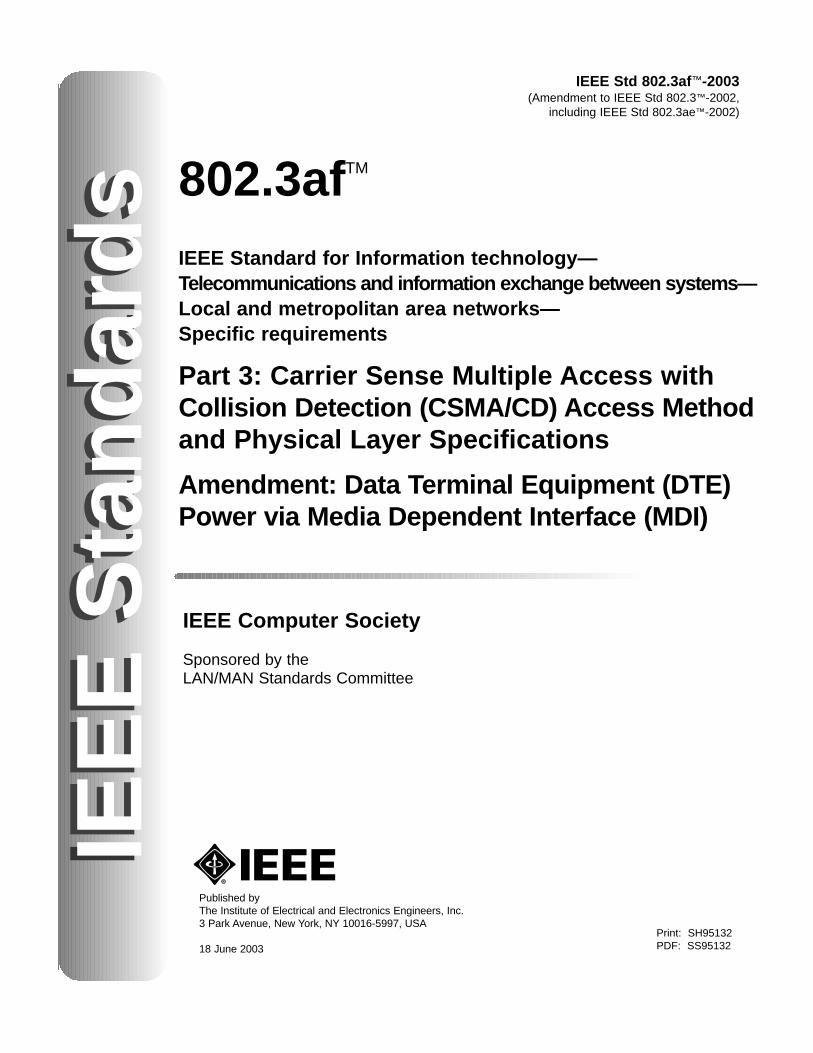
IEEE Std 802.3af™-2003(Amendment to IEEE Std 802.3™-2002,
including IEEE Std 802.3ae™-2002)
IEE
E S
tan
dar
ds 802.3afTM
IEEE Standard for Information technology—Telecommunications and information exchange between systems—Local and metropolitan area networks—Specific requirements
Part 3: Carrier Sense Multiple Access withCollision Detection (CSMA/CD) Access Methodand Physical Layer Specifications
Amendment: Data Terminal Equipment (DTE)Power via Media Dependent Interface (MDI)
Published by The Institute of Electrical and Electronics Engineers, Inc.3 Park Avenue, New York, NY 10016-5997, USA
18 June 2003
IEEE Computer Society
Sponsored by theLAN/MAN Standards Committee
IEE
E S
tan
dar
ds
Print: SH95132PDF: SS95132

The Institute of Electrical and Electronics Engineers, Inc.
3 Park Avenue, New York, NY 10016-5997, USA
Copyright © 2003 by the Institute of Electrical and Electronics Engineers, Inc.All rights reserved. Published 18 June 2003. Printed in the United States of America.
IEEE and 802 are registered trademarks in the U.S. Patent & TrademarkOffice, owned by the Institute of Electrical and Electronics Engineers, Incorporated.
Print:
ISBN 0-7381-3696-4 SH95132
PDF:
ISBN 0-7381-3697-2 SS95132
No part of this publication may be reproduced in any form, in an electronic retrieval system or otherwise, without the prior written permission of the publisher.
IEEE Std 802.3af
™
-2003
(Amendment to IEEE Std 802.3
™
-2002,including IEEE Std 802.3ae
™
-2002)
IEEE Standard for Information technology—Telecommunications and information exchange between systems—Local and metropolitan area networks—Specific requirements
Part 3: Carrier Sense Multiple Access withCollision Detection (CSMA/CD) Access Methodand Physical Layer Specifications
Amendment: Data Terminal Equipment (DTE) Power via Media Dependent Interface (MDI)
Sponsor
LAN/MAN Standards Committee
of the
IEEE Computer Society
Approved 12 June 2003
IEEE-SA Standards Board
Abstract:
Support for optionally powering a 10BASE-T, 100BASE-TX or 1000BASE-T DTE devicevia the Power Interface (PI) using physical layers defined in Clauses 14, 25, and 40. The PowerSourcing Equipment (PSE) is located at an endpoint or midspan, separate from and between theMDIs, and provides power to the Powered Device (PD) over the Link Section. The PSE detectionprotocol distinguishes a compatible PD from non-compatible devices and precludes the applicationof power and possible damage to non-compatible devices. The PSE monitors the Maintain PowerSignature (MPS) and removes power when it is no longer requested or required. Optional manage-ment function requirements are specified.
Keywords:
802.3af, Link Section, midspan, MPS, PD, PI, POE, power, Power over Ethernet, PSE
IEEE Standards
documents are developed within the IEEE Societies and the Standards Coordinating Committees of theIEEE Standards Association (IEEE-SA) Standards Board. The IEEE develops its standards through a consensus develop-ment process, approved by the American National Standards Institute, which brings together volunteers representing variedviewpoints and interests to achieve the final product. Volunteers are not necessarily members of the Institute and serve with-out compensation. While the IEEE administers the process and establishes rules to promote fairness in the consensus devel-opment process, the IEEE does not independently evaluate, test, or verify the accuracy of any of the information contained inits standards.
Use of an IEEE Standard is wholly voluntary. The IEEE disclaims liability for any personal injury, property or other damage,of any nature whatsoever, whether special, indirect, consequential, or compensatory, directly or indirectly resulting from thepublication, use of, or reliance upon this, or any other IEEE Standard document.
The IEEE does not warrant or represent the accuracy or content of the material contained herein, and expressly disclaims anyexpress or implied warranty, including any implied warranty of merchantability or fitness for a specific purpose, or that theuse of the material contained herein is free from patent infringement. IEEE Standards documents are supplied “
AS IS
.”
The existence of an IEEE Standard does not imply that there are no other ways to produce, test, measure, purchase, market,or provide other goods and services related to the scope of the IEEE Standard. Furthermore, the viewpoint expressed at thetime a standard is approved and issued is subject to change brought about through developments in the state of the art andcomments received from users of the standard. Every IEEE Standard is subjected to review at least every five years for revi-sion or reaffirmation. When a document is more than five years old and has not been reaffirmed, it is reasonable to concludethat its contents, although still of some value, do not wholly reflect the present state of the art. Users are cautioned to checkto determine that they have the latest edition of any IEEE Standard.
In publishing and making this document available, the IEEE is not suggesting or rendering professional or other services for,or on behalf of, any person or entity. Nor is the IEEE undertaking to perform any duty owed by any other person or entity toanother. Any person utilizing this, and any other IEEE Standards document, should rely upon the advice of a competent pro-fessional in determining the exercise of reasonable care in any given circumstances.
Interpretations: Occasionally questions may arise regarding the meaning of portions of standards as they relate to specificapplications. When the need for interpretations is brought to the attention of IEEE, the Institute will initiate action to prepareappropriate responses. Since IEEE Standards represent a consensus of concerned interests, it is important to ensure that anyinterpretation has also received the concurrence of a balance of interests. For this reason, IEEE and the members of its soci-eties and Standards Coordinating Committees are not able to provide an instant response to interpretation requests except inthose cases where the matter has previously received formal consideration.
Comments for revision of IEEE Standards are welcome from any interested party, regardless of membership affiliation withIEEE. Suggestions for changes in documents should be in the form of a proposed change of text, together with appropriatesupporting comments. Comments on standards and requests for interpretations should be addressed to:
Secretary, IEEE-SA Standards Board
445 Hoes Lane
P.O. Box 1331
Piscataway, NJ 08855-1331
USA
Authorization to photocopy portions of any individual standard for internal or personal use is granted by the Institute of Elec-trical and Electronics Engineers, Inc., provided that the appropriate fee is paid to Copyright Clearance Center. To arrange forpayment of licensing fee, please contact Copyright Clearance Center, Customer Service, 222 Rosewood Drive, Danvers, MA01923 USA; +1 978 750 8400. Permission to photocopy portions of any individual standard for educational classroom usecan also be obtained through the Copyright Clearance Center.
Note: Attention is called to the possibility that implementation of this standard may require use of subject mat-ter covered by patent rights. By publication of this standard, no position is taken with respect to the existence orvalidity of any patent rights in connection therewith. The IEEE shall not be responsible for identifying patentsfor which a license may be required by an IEEE standard or for conducting inquiries into the legal validity orscope of those patents that are brought to its attention.
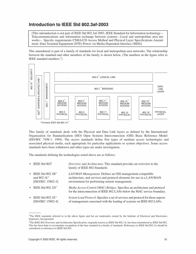
Introduction to IEEE Std 802.3af-2003
[This introuduction is not part of IEEE Std 802.3af-2003, IEEE Standard for Information technology—Telecommunications and information exchange between systems—Local and metropolitan area net-works— Specific requirements CSMA/CD Access Method and Physical Layer Specifications Amend-ment: Data Terminal Equipment (DTE) Power via Media Dependent Interface (MDI)]
This amendment is part of a family of standards for local and metropolitan area networks. The relationshipbetween the standard and other members of the family is shown below. (The numbers in the figure refer toIEEE standard numbers.1)
This family of standards deals with the Physical and Data Link layers as defined by the InternationalOrganization for Standardization (ISO) Open Systems Interconnection (OSI) Basic Reference Model(ISO/IEC 7498-1: 1994). The access standards define five types of medium access technologies andassociated physical media, each appropriate for particular applications or system objectives. Some accessstandards have been withdrawn and other types are under investigation.
The standards defining the technologies noted above are as follows:
1The IEEE standards referred to in the above figure and list are trademarks owned by the Institute of Electrical and ElectronicsEngineers, Incorporated.2The IEEE 802 Overview and Architecture Specification, originally known as IEEE Std 802.1A, has been renumbered as IEEE Std 802.This has been done to accomodate recognition of the base standard in a family of standards. References to IEEE Std 802.1A should beconsidered as references to IEEE Std 802.
• IEEE Std 802 Overview and Architecture. This standard provides an overview to the family of IEEE 802 Standards.
• IEEE Std 802.1B™
and 802.1k™
[ISO/IEC 15802-2]
LAN/MAN Management. Defines an OSI management-compatible architecture, and services and protocol elements for use in a LAN/MAN environment for performing remote management.
• IEEE Std 802.1D™ Media Access Control (MAC) Bridges. Specifies an architecture and protocol for the interconnection of IEEE 802 LANs below the MAC service boundary.
• IEEE Std 802.1E™
[ISO/IEC 15802-4]System Load Protocol. Specifies a set of services and protocol for those aspects of management concerned with the loading of systems on IEEE 802 LANs.
* Formerly IEEE Std 802.1A.
DATALINK
LAYER
PHYSICAL
802.2 LOGICAL LINK
802.1 BRIDGING
802.
1 M
AN
AG
EM
EN
T
802
OV
ER
VIE
W &
AR
CH
ITE
CTU
RE
*
802.
10
SE
CU
RIT
Y
802.3
MEDIUMACCESS
.
802.3PHYSICAL
802.5
MEDIUMACCESS
802.5PHYSICAL
802.11
MEDIUMACCESS
802.11PHYSICAL LAYER
802.16
MEDIUMACCESS
802.16PHYSICAL
802.15
MEDIUMACCESS
802.15PHYSICAL
2
Copyright © 2003 IEEE. All rights reserved. iii
Conformance test methodology
An additional standard, IEEE Std 1802.3
™
provides conformance test information for 10BASE-T.
IEEE Std 802.3af-2003
This standard contains state-of-the-art material. The area covered by this standard is undergoing evolution.Revisions are anticipated to this standard within the next few years to clarify existing material, to correctpossible errors, and to incorporate new related material.
• IEEE Std 802.1F
™
Common Definitions and Procedures for IEEE 802 Management Information
.
• IEEE Std 802.1G
™
[ISO/IEC 15802-5]
Remote Media Access Control
(MAC) Bridging
. Specifies extensions for the interconnection, using non-LAN communication technologies, of geographically separated IEEE 802 LANs below the level of the logical link control protocol.
• IEEE Std 802.1H
™
[ISO/IEC TR 11802-5]
Media Access Control (MAC) Bridging of Ethernet V2.0 in Local Area Networks
.
• IEEE Std 802.2[ISO/IEC 8802-2]
Logical Link Control.
• IEEE Std 802.3
CSMA/CD Access Method and Physical Layer Specifications.
• IEEE Std 802.5[ISO/IEC 8802-5]
Token Ring Access Method and Physical Layer Specifications.
• IEEE Std 802.10
Interoperable LAN/MAN Security.
• IEEE Std 802.11[ISO/IEC DIS 8802-11]
Wireless LAN Medium Access Control (MAC) and Physical Layer Specifications.
• IEEE Std 802.15
Wireless Medium Access Control (MAC) and Physical Layer (PHY)Specifications for: Wireless Personal Area Networks.
• IEEE Std 802.16
Standard Air Interface for Fixed Broadband Wireless Access Systems.
In addition to the family of standards, the following is a recommended practice for a common PhysicalLayer technology:
• IEEE Std 802.7
™
IEEE Recommended Practice for Broadband Local Area Networks.
iv Copyright © 2003 IEEE. All rights reserved.

Participants
The following is a list of chairs and editors at the time the IEEE 802.3 Working Group balloted this standard:
Geoffrey O. Thompson,
Chair—Phase 1
Robert M. Grow,
Chair—Phase 2
David J. Law,
Vice Chair
Robert M. Grow,
Secretary—Phase 1
Steven B. Carlson,
Secretary—Phase 2
Steven B. Carlson,
Chair, 802.3af Task Force
Michael S. McCormack,
Editor—Phase 1, 802.3af Task Force
John J. Jetzt,
Editor—Phase 2, 802.3af Task Force
Chad M. Jones,
Comment
Editor, 802.3af Task Force
The following is a list of voters at the time the IEEE 802.3 Working Group balloted this standard: Martin AdamsOscar AgazziDon AlderrouThomas AlexanderKhaled AmerKeith AmundsenTony AndersonRalph AnderssonJack AndresenMehran AtaeePhil AuldGerard E. BachandAndy BaldmanHugh BarrassBob BarrettHoward BaumerDenis BeaudoinMichaël BeckMike BennettSidney BerglundJohn L. BestelVipul BhattJeff E. BisbergMichel BohbotBrad BoothPaul BottorffGary BourqueKirk BovillRichard BrandAndrew Brierley-GreenRhett BrikovskisRick BrooksBenjamin BrownKevin BrownSteve F. BuckLisa BuckmanJames BurgessScott BurtonRobert BusseRoy BynumDonald CaldwellRichard CamJustin ChangXiaopeng ChenZinan ChenHon Wah ChinKuen ChowGeorge ClasemanTerry Cobb
Doug ColemanRégis CollaHerb CongdonEdward CornejoRichard CrossBrian CruikshankChris CullinDavid CunninghamJohn D'AmbrosiaRobert DahlgrenKevin DainesJohn DallesasseRupert S. DanceYair DarshanPeter DartnellPiers DaweMichael deBieTom DebiecJoel DedrickChris Di MinicoWael DiabThomas DineenHamish DobsonDavid W. DolfiDan DoveDaniel S. DraperBrian DreverMike DudekRichard DuganDavid DwelleyClay EddingsFrank J. EffenbergerJohn EganGeorge EislerMartin ElhøjJohn F. EwenJean-Loup FerrantJens FiedlerNorival FigueiraRobert G. FinchFarzin FiroozmandAlan FlatmanRoger FraserHoward FrazierLadd FreitagKrister FrojdhYukihiro FujimotoDarrell FurlongJustin Gaither
Denton GentryJohn GeorgeAli GhiasiPat GillilandMoty GoldisMatthew GoldmanTimothy D. GoodmanRich GrahamEric B. GrannC. Thomas GrayJonathan E. GreenlawAjay GummallaMichael HackertStephen HaddockSharam HakimiFarid HamidyJohannes HansenDel HansonMarwan HassounTom HatleyAdam HealeyRonen HeldmanItzik HendelKen HerrityJames H. HessonHenry HinrichsDavid HinzelRyan HirthJay HogeDavid W. HyerHaruhiko IchinoOsamu IshidaSteve JacksonMichael R. JacobsonBrent JaffaEric JangWoo-Hyuk JangJack L. JewellWenbin JiangClarence JohDavid KabalShinkyo KakuMohan KalkuntePuru KamatRoger KaramDave KaufmanN. Patrick KellyJohn J. KennyDawson Kesling
David E. KohlPaul KolesarGlen KramerGerard KuytHans LacknerLawrence J. LamersWilliam LaneDaun LangstonRyan LatchmanQuang LeEugene LeeWesley LeeAmir LehrLisa LeoRobert H. LeonowichAvinoam LevyTom LindsayFengkun LiuFred A. LucasMeilissa R. LumJeffrey LynchEric R. LynskeyHenning LysdalBrian MacLeodAriel MaislosDavid W. MartinKoichiro MashikoThomas MatheyZiad Albert MatniHideyuki MatsuoBob MayerKent McCammonPhilip L. McCarronJo Beth MetzgerRichard MichalowskiJacob (Kobi) MizrahiFred MohamadiDirk S. MohlCindy MontstreamPaul B. MooreRobert MooreShohei MoriwakiRobert MuirShimon MullerDenis MurphyThomas MurphyBrian MurrayGerard NadeauKen Naganuma
Copyright © 2003 IEEE. All rights reserved. v

Hari NaiduKarl NakamuraNersi NazariKristian NelsonPaul NikolichMichael NootbaarBob NoseworthySatoshi ObaraStephen OhPeter OhlénToshio OokaPhilip OrlikGeorge OughtonRobert R. PaceDon PannellElwood T. ParsonsDipak M. PatelAlex PavlovskyJohn PaynePetar PepeljugoskiGerry PesaventoArmin PitzerTimothy R. PlunkettJeff PorterWilliam QuackenbushJim QuiliciPatrick W. Quinn
John QuirkRick RabinovichJurgen RahnNaresh RamanJennifer G. RasimasDan RauschPeter RautenbergMaurice ReintjesLawrence RennieRamez RizkShawn RogersDan RomascanuTume RömerFloyd RossLarry RubinHyunsurk RyuDolors SalaAnthony SandersMark SankeyAkira SasakiRaj SavaraKlaus SchulzPeter SchwartzKhorvash SefidvashSteve SeleeKoichiro SetoVadim Shain
Robbie ShergillJian SongPatrick H. StanleyNick StapletonClaus StetterDonald S. StewartDean M. StoddartMario StoltzHiroshi SuzukiDaniel SvenssonSteve SwansonTad SzostakRich TaborekBharat TailorAkio TajimaMike TatePat ThalerR. Jonathan ThatcherWalter ThirionBruce TolleyPaul TorgersonRick TownsendEdward TurnerBulent TusirayBor-long TwuSterling A. VadenSchelto van Doorn
Peter Van LaanenErik van OostenVinod Kumar VenkatavaratonRamakrishna VepaGérard VergnaudDavid VogelMartin WagnerTim WarlandJeff WarrenTed WashburnFred WenigerTony WhitlowBill WiedemannJohn WolcottKing WonShin-Hee WonDavid WongEdward WongLeo WongPercy WongStefan M. WursterDoug YoderJason YorksLeonard YoungHank ZanniniBob Zona
vi Copyright © 2003 IEEE. All rights reserved.

The following members of the balloting committee voted on this revision of the standard. Balloters mayhave voted for approval, disapproval, or abstention.
When the IEEE-SA Standards Board approved this standard on 12 June 2003, it had the followingmembership:
Don Wright,
Chair
Howard M. Frazier,
Vice Chair
Judith Gorman,
Secretary
*Member Emeritus
Also included are the following nonvoting IEEE-SA Standards Board liaisons:
Alan Cookson,
NIST Representative
Satish K. Aggarwal,
NRC Representative
Catherine Berger
IEEE Standards Project Editor
Ilian AtiasJacob Ben AryBenjamin BrownScott BurtonJeff CainSteven B. CarlsonYawgeng ChauKeith ChowChris CullinGuru Dutt DhingraYair DarshanWael DiabChristopher T. DiminicoThomas DineenDr. Sourav DuttaDavid McLean DwellyMordechai GoldisRich GrahamRobert M. GrowStephen HaddockKhosrow Haratian
Marian HargisSteven M. HemmahPeeya IwagoshiRaj JainJohn J. JetztChad JonesRoger A. KaramE. S. KramerWilliam LaneDavid J. LawPi-Cheng LawAmir LehrDaniel LevesqueVincent LipsioJeff LynchJose MoralesAhmad MahinfallahKyle MausPatrick McCaugheyMichael McCormackSteve Methley
George MiaoJoseph MoranRobert MuirKen NaganumaPaul NikolichBob O'HaraSatoshi ObaraDonald R. PannellSubbu PonnuswamyVikram PunjMaurice ReintjesThomas RufFrederick SchindlerCharles SpurgeonClay StocklinSteven SwansonPat ThalerGeoffrey O. ThompsonJerry ThrasherSterling VadenOren Yuen
H. Stephen BergerJoe BruderBob DavisRichard DeBlasioJulian Forster*Toshio FukudaArnold M. GreenspanRaymond Hapeman
Donald M. HeirmanLaura HitchcockRichard H. HulettAnant JainLowell G. JohnsonJoseph L. Koepfinger*Tom McGeanSteve Mills
Daleep C. MohlaWilliam J. MoylanPaul NikolichGary RobinsonMalcolm V. ThadenGeoffrey O. ThompsonDoug ToppingHoward L. Wolfman
Copyright © 2003 IEEE. All rights reserved
. vii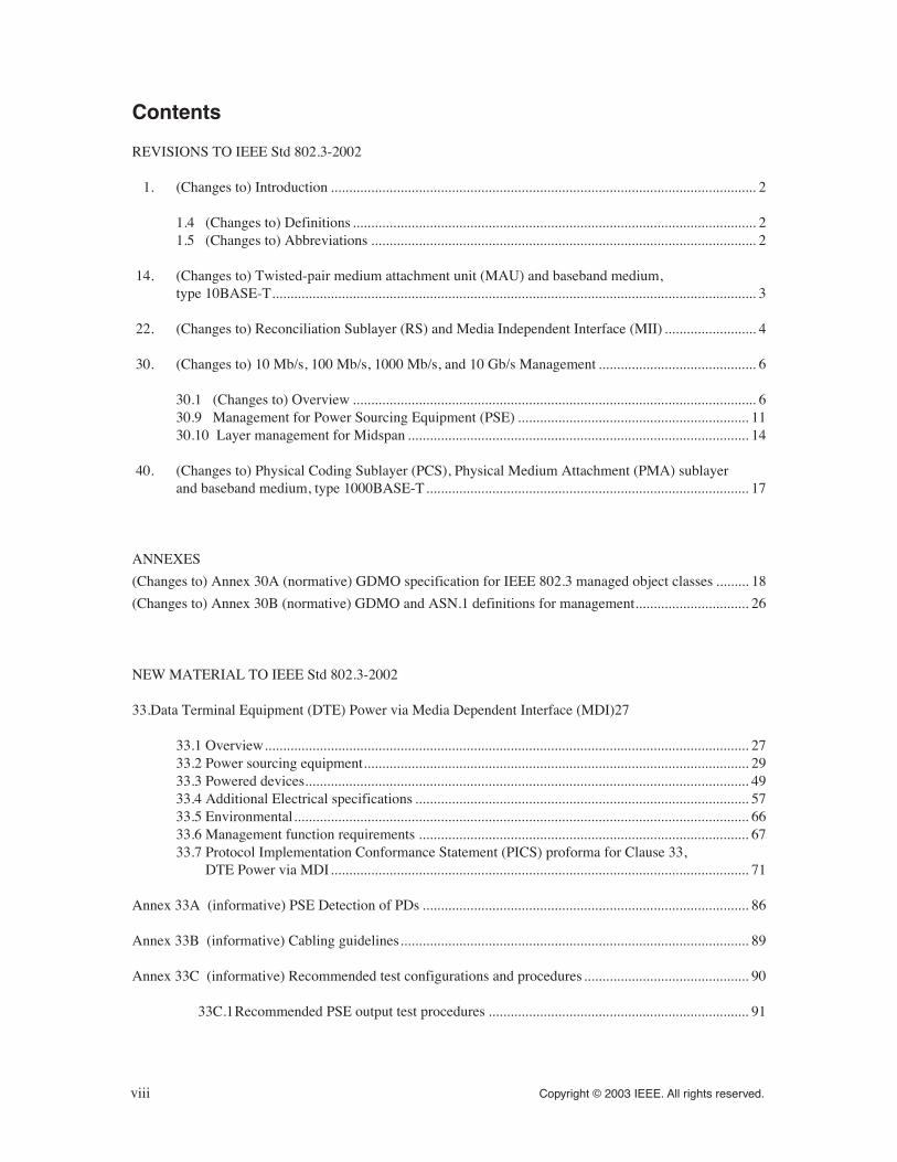
Contents
REVISIONS TO IEEE Std 802.3-2002
1. (Changes to) Introduction .................................................................................................................... 2
1.4 (Changes to) Definitions .............................................................................................................. 21.5 (Changes to) Abbreviations ......................................................................................................... 2
14. (Changes to) Twisted-pair medium attachment unit (MAU) and baseband medium, type 10BASE-T.................................................................................................................................... 3
22. (Changes to) Reconciliation Sublayer (RS) and Media Independent Interface (MII) ......................... 4
30. (Changes to) 10 Mb/s, 100 Mb/s, 1000 Mb/s, and 10 Gb/s Management ........................................... 6
30.1 (Changes to) Overview .............................................................................................................. 630.9 Management for Power Sourcing Equipment (PSE) ............................................................... 1130.10 Layer management for Midspan ............................................................................................. 14
40. (Changes to) Physical Coding Sublayer (PCS), Physical Medium Attachment (PMA) sublayerand baseband medium, type 1000BASE-T........................................................................................ 17
ANNEXES
(Changes to) Annex 30A (normative) GDMO specification for IEEE 802.3 managed object classes ......... 18
(Changes to) Annex 30B (normative) GDMO and ASN.1 definitions for management............................... 26
NEW MATERIAL TO IEEE Std 802.3-2002
33.Data Terminal Equipment (DTE) Power via Media Dependent Interface (MDI)27
33.1 Overview.................................................................................................................................... 2733.2 Power sourcing equipment......................................................................................................... 2933.3 Powered devices......................................................................................................................... 4933.4 Additional Electrical specifications ........................................................................................... 5733.5 Environmental............................................................................................................................ 6633.6 Management function requirements .......................................................................................... 6733.7 Protocol Implementation Conformance Statement (PICS) proforma for Clause 33,
DTE Power via MDI.................................................................................................................. 71
Annex 33A (informative) PSE Detection of PDs ......................................................................................... 86
Annex 33B (informative) Cabling guidelines............................................................................................... 89
Annex 33C (informative) Recommended test configurations and procedures............................................. 90
33C.1Recommended PSE output test procedures ....................................................................... 91
viii Copyright © 2003 IEEE. All rights reserved.
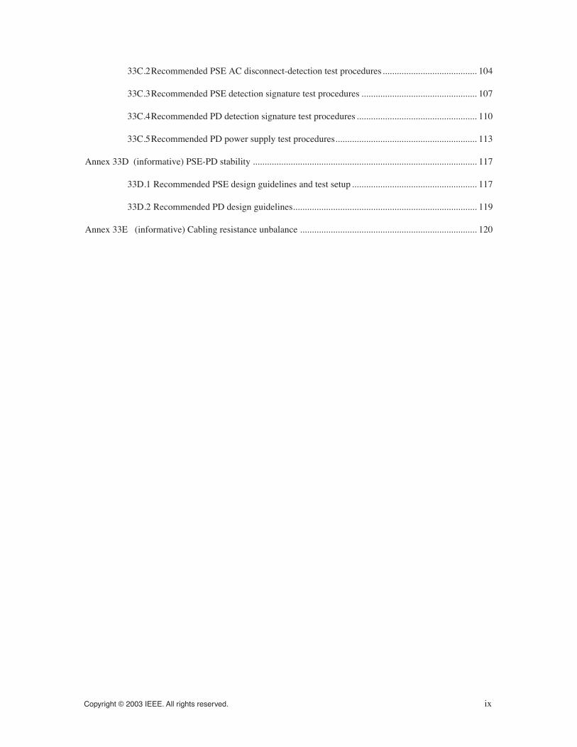
33C.2Recommended PSE AC disconnect-detection test procedures........................................ 104
33C.3Recommended PSE detection signature test procedures ................................................. 107
33C.4Recommended PD detection signature test procedures ................................................... 110
33C.5Recommended PD power supply test procedures............................................................ 113
Annex 33D (informative) PSE-PD stability ............................................................................................... 117
33D.1 Recommended PSE design guidelines and test setup ..................................................... 117
33D.2 Recommended PD design guidelines.............................................................................. 119
Annex 33E (informative) Cabling resistance unbalance ........................................................................... 120
Copyright © 2003 IEEE. All rights reserved. ix
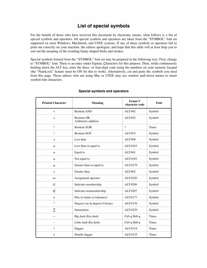
List of special symbols
For the benefit of those who have received this document by electronic means, what follows is a list ofspecial symbols and operators. All special symbols and operators are taken from the “SYMBOL” font setsupported on most Windows, MacIntosh, and UNIX systems. If any of these symbols or operators fail toprint out correctly on your machine, the editors apologize, and hope that this table will at least help you tosort out the meaning of the resulting funny-shaped blobs and strokes.
Special symbols formed from the “SYMBOL” font set may be prepared in the following way: First, changeto “SYMBOL” font. There is an entry under Format, Characters for this purpose. Then, while continuouslyholding down the ALT key, enter the three- or four-digit code using the numbers on your numeric keypad(the “NumLock” feature must be ON for this to work). Alternatively, cut and paste the symbols you needfrom this page. Those editors who are using Mac or UNIX may use window pull-down menus to insertsymbol-font characters.
Special symbols and operators
Printed Character Meaning Frame Vcharacter code Font
∗ Boolean AND ALT-042 Symbol
+ Boolean OR,Arithmetic addition
ALT-043 Symbol
^ Boolean XOR ^ Times
! Boolean NOT ALT-033 Symbol
< Less than ALT-060 Symbol
≤ Less than or equal to ALT-0163 Symbol
= Equal to ALT-061 Symbol
≠ Not equal to ALT-0185 Symbol
≥ Greater than or equal to ALT-0179 Symbol
> Greater than ALT-062 Symbol
⇐ Assignment operator ALT-0220 Symbol
∈ Indicates membership ALT-0206 Symbol
∉ Indicates nonmembership ALT-0207 Symbol
± Plus or minus (a tolerance) ALT-0177 Symbol
° Degrees (as in degrees Celsius) ALT-0176 Symbol
∑ Summation ALT-0229 Symbol
— Big dash (Em dash) Ctrl-q Shft-q Times
– Little dash (En dash) Ctrl-q Shft-p Times
† Dagger ALT-0134 Times
‡ Double dagger ALT-0135 Times
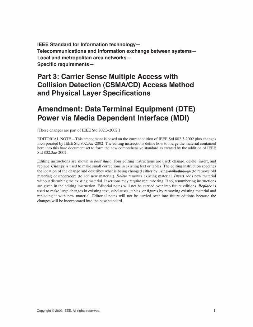
IEEE Standard for Information technology—Telecommunications and information exchange between systems—Local and metropolitan area networks—Specific requirements—
Part 3: Carrier Sense Multiple Access withCollision Detection (CSMA/CD) Access Methodand Physical Layer Specifications
Amendment: Data Terminal Equipment (DTE) Power via Media Dependent Interface (MDI)[These changes are part of IEEE Std 802.3-2002.]
EDITORIAL NOTE—This amendment is based on the current edition of IEEE Std 802.3-2002 plus changesincorporated by IEEE Std 802.3ae-2002. The editing instructions define how to merge the material containedhere into this base document set to form the new comprehensive standard as created by the addition of IEEEStd 802.3ae-2002.
Editing instructions are shown in bold italic. Four editing instructions are used: change, delete, insert, andreplace. Change is used to make small corrections in existing text or tables. The editing instruction specifiesthe location of the change and describes what is being changed either by using strikethrough (to remove oldmaterial) or underscore (to add new material). Delete removes existing material. Insert adds new materialwithout disturbing the existing material. Insertions may require renumbering. If so, renumbering instructionsare given in the editing instruction. Editorial notes will not be carried over into future editions. Replace isused to make large changes in existing text, subclauses, tables, or figures by removing existing material andreplacing it with new material. Editorial notes will not be carried over into future editions because thechanges will be incorporated into the base standard.
Copyright © 2003 IEEE. All rights reserved. 1
IEEE Std 802.3af-2003 AMENDMENT TO IEEE Std 802.3
1. Introduction
1.4 Definitions
Replace 1.4.170 with the following:
1.4.170 Medium Dependent Interface (MDI): The mechanical and electrical or optical interface betweenthe transmission medium and the MAU (e.g., 10BASE-T) or the PHY (e.g., 1000BASE-T) and also betweenthe transmission medium and any associated (optional per IEEE 802.3 Clause 33) Powered Device (PD) orEndpoint Power Sourcing Equipment (PSE).
Insert the following definitions alphabetically into 1.4. Renumber the definitions as required.
1.4.x Endpoint PSE: Power Sourcing Equipment (PSE) that is located at an endpoint.
1.4.x Link Section: The portion of the link from the PSE to the PD.
1.4.x Midspan: An entity located within a link segment that is distinctly separate from and between theMedium Dependent Interfaces (MDIs).
1.4.x Midspan PSE: Power Sourcing Equipment (PSE) that is located in the Midspan.
1.4.x PSE Group: A PSE or a collection of PSEs that can be related to the logical arrangement for manage-ment within an encompassing system.
1.4.x Power Interface (PI): The mechanical and electrical interface between the Power Sourcing Equip-ment (PSE) or Powered Device (PD) and the transmission medium. In an Endpoint PSE and in a PD thePower Interface is the MDI.
1.4.x Twisted Pair Medium Dependent Interface (TP MDI): The mechanical and electrical interfacebetween the transmission medium and the Medium Attachment Unit (MAU) or PHY, e.g., (10BASE-T,100BASE-TX, or 1000BASE-T).
1.4.x Power Sourcing Equipment (PSE): A DTE or midspan device that provides the power to a single linksection. DTE powering is intended to provide a single 10BASE-T, 100BASE-TX, or 1000BASE-T devicewith a unified interface for both the data it requires and the power to process these data.
1.4.x Powered Device (PD): A device that is either drawing power or requesting power from a PSE.
1.5 Abbreviations
Insert the following items alphabetically in 1.5.
MPS Maintain Power SignaturePD Powered DevicePI Power InterfacePSE Power Sourcing EquipmentSELV Safety Extra Low Voltage
2 Copyright © 2003 IEEE. All rights reserved.
IEEE
CSMA/CD Std 802.3af-2003
Copyright © 2003 IEEE. All rights reserved.
3
14. Twisted-pair medium attachment unit (MAU) and baseband medium, type 10BASE-T
14.3.1.1 Isolation requirement
Change the first paragraph of this subclause as follows:
A MAU that encompasses the PI of a PD within its MDI (see 33.1.3) shall provide isolation between allexternal conductors, including frame ground, and all MDI leads including those not used by 10BASE-T. AMAU that does not encompass the PI of a PD within its MDIthe MAU shall provide isolation between theDTE Physical Layer circuits including frame ground and all MDI leads including those not used by10BASE-T. This electrical separation shall withstand at least one of the following electrical strength tests.
14.10.4.5.11 Isolation requirements
Replace item 1 of the table in this subclause with the following:
1a Isolation, MDI leads to DTE Physical Layer circuits 14.3.1.1 C
Any of the three tests listed in 14.3.1.1. Function provided by MAUs that do not encompass the PI of a PD within their MDI.
1b Isolation, MDI leads to all external conductors 14.3.1.1 C
Any of the three tests listed in 14.3.1.1. Function provided by MAUs that encompass the PI of a PD within their MDI.
IEEE Std 802.3af-2003 AMENDMENT TO IEEE Std 802.3
22. Reconciliation Sublayer (RS) and Media Independent Interface (MII)
22.2.4 Management functions
Change the third paragraph of this subclause as follows:
The MII basic register set consists of two registers referred to as the Control register (Register 0) and the Sta-tus register (Register 1). All PHYs that provide an MII shall incorporate the basic register set. All PHYs thatprovide a GMII shall incorporate an extended basic register set consisting of the Control register (Register0), Status register (Register 1), and Extended Status register (Register 15). The status and control functionsdefined here are considered basic and fundamental to 100 Mb/s and 1000 Mb/s PHYs. Registers 2 through1012 are part of the extended register set. The format of Registers 4 through 10 are defined for the specificAuto-Negotiation protocol used (Clause 28 or Clause 37). The format of these registers is selected by the bitsettings of Registers 1 and 15.
Change Table 22–6 as follows:
Table 22–6—MII management register set
Register address Register nameBasic/Extended
MII GMII
0 Control B B
1 Status B B
2,3 PHY Identifier E E
4 Auto-Negotiation Advertisement E E
5 Auto-Negotiation Link Partner Base Page Ability
E E
6 Auto-Negotiation Expansion E E
7 Auto-Negotiation Next Page Transmit E E
8 Auto-Negotiation Link Partner Received Next Page
E E
9 MASTER-SLAVE Control Register E E
10 MASTER-SLAVE Status Register E E
11 PSE Control register E E
12 PSE Status register E E
1113, through 14 Reserved E E
15 Extended Status Reserved B
16 through 31 Vendor Specific E E
4 Copyright © 2003 IEEE. All rights reserved.
IEEE
CSMA/CD Std 802.3af-2003
22.2.4.3 Extended capability registers
Change the first paragraph of this subclause as follows:
In addition to the basic register set defined in 22.2.4.1 and 22.2.4.2, PHYs may provide an extended set ofcapabilities that may be accessed and controlled via the MII management interface. ElevenNine registershave been defined within the extended address space for the purpose of providing a PHY-specific identifierto layer management, and to provide control and monitoring for the Auto-Negotiation process, and to pro-vide control and monitoring of power sourcing equipment.
Add the following two new subclauses after subclause 22.2.4.3.8 and renumber current subclause22.2.4.3.9 as 22.2.4.3.11.
22.2.4.3.9 PSE Control register (Register 11)
Register 11 provides control bits that are used by a PSE. See 33.6.1.1.
22.2.4.3.10 PSE Status register (Register 12)
Register 12 provides status bits that are supplied by a PSE. See 33.6.1.2.
Copyright © 2003 IEEE. All rights reserved. 5
IEEE Std 802.3af-2003 AMENDMENT TO IEEE Std 802.3
30. 10 Mb/s, 100 Mb/s, 1000 Mb/s and 10 Gb/s Management
30.1 Overview
Change the first paragraph of this subclause as follows:
This clause provides the Layer Management specification for DTEs, repeaters, and MAUs, and Midspansbased on the CSMA/CD access method. The clause is produced from the ISO framework additions toClause 5, Layer Management; Clause 19, Repeater Management; and Clause 20, MAU Management. Itincorporates additions to the objects, attributes, and behaviors to support 100 Mb/s, 1000 Mb/s and 10 Gb/s,full duplex operation, MAC Control, and Link Aggregation and DTE Power via MDI.
30.1.1 Scope
Change the first paragraph of this subclause as follows:
This clause includes selections from Clauses 5, 19, and 20. It is intended to be an entirely equivalent specifi-cation for the management of 10 Mb/s DTEs, 10 Mb/s baseband repeater units, and 10 Mb/s integratedMAUs. It also includes the additions for management of MAC Control, DTEs and repeaters at speeds greaterthan 10 Mb/s, embedded MAUs, and PHYs and DTE Power via MDI. Implementations of management forDTEs, repeater units, and embedded MAUs should follow the requirements of this clause (e.g., a 10 Mb/simplementation should incorporate the attributes to indicate that it is not capable of 100 or 1000 Mb/soperation,; half duplex DTE should incorporate the attributes to indicate that it is not capable of full duplexoperation, etc.).
30.1.2 Relationship to objects in IEEE 802.1F
Change the second paragraph of this subclause as follows:
oResourceTypeIDThis object class is mandatory and shall be implemented as defined in IEEE 802.1F. This object is bound to oMAC-Entity, oRepeater, oMidSpan and oMAU as defined by the NAME BINDINGs in 30A.8.130A.10.1. Note that the binding to oMAU is mandatory only when MII is present. The Entity Relationship Diagrams, Figures 30–3 and 30–4, shows these bindings pictorially.
30.1.4 Management model
Change the second last paragraph of this subclause as follows:
The above items are defined in 30.3, 30.4, 30.5, 30.6, 30.7 and 30.8 through 30.10 of this clause in terms ofthe template requirements of ISO/IEC 10165-4: 1991.
30.2.2.1 Text description of managed objects
Insert the following text immediately after the description of oWIS:
oMidSpanThe top-most managed object class of the Midspan containment tree shown in Figure 30–4. Note that this managed object class may be contained within another superior managed object class. Such containment is expected, but is outside the scope of this standard.
6 Copyright © 2003 IEEE. All rights reserved.
IEEE
CSMA/CD Std 802.3af-2003
oPSEGroupThe PSE Group managed object class is a view of a collection of PSEs.
oPSEThe managed object of that portion of the containment trees shown in Figure 30–3 and Figure 30–4. The attributes and actions defined in this subclause are contained within the oPSE managed object.
30.2.3 Containment
Change the first paragraph of this subclause as follows:
A containment relationship is a structuring relationship for managed objects in which the existence of amanaged object is dependent on the existence of a containing managed object. The contained managedobject is said to be the subordinate managed object, and the containing managed object the superior man-aged object. The containment relationship is used for naming managed objects. The local containment rela-tionships among object classes are depicted in the entity relationship diagrams, Figure 30–3 and Figure 30–4. This These figures shows the names of the object classes and whether a particular containment relation-ship is one-to-one or one-to-many. For further requirements on this topic, see IEEE Std 802.1F-1993. PSEmanagement is only valid in a system that provides management at the next higher containment level, that is,either a DTE, repeater or Midspan with management.
Copyright © 2003 IEEE. All rights reserved. 7
IEEE Std 802.3af-2003 AMENDMENT TO IEEE Std 802.3
Replace the existing Figure 30–3 with the following new figure:
oResourceTypeID
Present if MII
Figure 30–3—Repeater and DTE System Eentity relationship diagram
oRepeater30.4.1
oResourceTypeID oGroup30.4.2
oRepeaterPort30.4.3
oMAU30.5.1
oAutoNegotiation30.6.1
oMACControlEntity30.3.3
oMACEntity30.3.1
oPHYEntity30.3.2
oMAU30.5.1
oAutoNegotiation30.6.1
oResourceTypeID
oMACControlFunctionEntity30.3.4
Denotes one-to-many relationship
Denotes one-to-one relationship
Repeater System DTE System
oAggregator30.7.1
oAggregationPort30.7.2
oAggPortStats30.7.3
oAggPortDebugInformation30.7.4
oWIS30.8.1
oPSE30.9.1
oPSE30.9.1
oResourceTypeID
Present if MII
8 Copyright © 2003 IEEE. All rights reserved.
IEEE
CSMA/CD Std 802.3af-2003
Insert new Figure 30–4 as follows:
30.2.5 Capabilities
Change the first paragraph of this subclause as follows:
This standard makes use of the concept of packages as defined in ISO/IEC 10165-4: 1992 as a means ofgrouping behaviour, attributes, actions, and notifications within a managed object class definition. Packagesmay either be mandatory, or be conditional, that is to say, present if a given condition is true. Within thisstandard capabilities are defined, each of which corresponds to a set of packages, which are components of anumber of managed object class definitions and which share the same condition for presence. Implementa-tion of the appropriate basic and mandatory packages is the minimum requirement for claiming conform-ance to IEEE 802.3 Management. Implementation of an entire optional capability is required in order toclaim conformance to that capability. The capabilities and packages for IEEE 802.3 Management are speci-fied in Tables 30–1, 30–2 and 30–3 through 30–4.
Insert the following paragraphs at the end of this subclause:
For managed PSEs, the PSE Basic Package is mandatory and the PSE Recommended Package is optional.For a managed PSE to be conformant to this standard, it shall fully implement the PSE Basic Package. For amanaged PSE to be conformant to the optional Recommended Package it shall implement that entire pack-age. PSE management is optional with respect to all other CSMA/CD management.
For managed Midspans, the Midspan managed object class shall be implemented in its entirety. All attributesand notifications are mandatory. Midspan management is optional with respect to all other CSMA/CDmanagement.
Figure 30–4—Midspan entity relationship diagram
oMidSpan30.10.1
oPSEGroup30.10.2
Midspan system
oPSE30.9.1
oResourceTypeID
Denotes one-to-many relationship
Denotes one-to-one relationship
Copyright © 2003 IEEE. All rights reserved. 9
IEEE Std 802.3af-2003 AMENDMENT TO IEEE Std 802.3
Insert the following new table after Table 30–3:
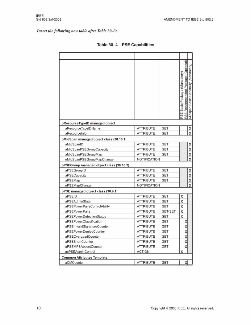
Table 30–4—PSE Capabilities
PS
E B
asic
Pac
kage
(M
anda
tory
)P
SE
Rec
omm
ende
d P
acka
ge (
Opt
iona
l)M
idsp
an B
asic
Cap
abili
ty (
Man
dato
ry)
oResourceTypeID managed object
aResourceTypeIDName ATTRIBUTE GET X
aResourceInfo ATTRIBUTE GET X
oMidSpan managed object class (30.10.1)
aMidSpanID ATTRIBUTE GET X
aMidSpanPSEGroupCapacity ATTRIBUTE GET X
aMidSpanPSEGroupMap ATTRIBUTE GET X
nMidSpanPSEGroupMapChange NOTIFICATION X
oPSEGroup managed object class (30.10.2)
aPSEGroupID ATTRIBUTE GET X
aPSECapacity ATTRIBUTE GET X
aPSEMap ATTRIBUTE GET X
nPSEMapChange NOTIFICATION X
oPSE managed object class (30.9.1)
aPSEID ATTRIBUTE GET X
aPSEAdminState ATTRIBUTE GET X
aPSEPowerPairsControlAbility ATTRIBUTE GET X
aPSEPowerPairs ATTRIBUTE GET-SET X
aPSEPowerDetectionStatus ATTRIBUTE GET X
aPSEPowerClassification ATTRIBUTE GET X
aPSEInvalidSignatureCounter ATTRIBUTE GET X
aPSEPowerDeniedCounter ATTRIBUTE GET X
aPSEOverLoadCounter ATTRIBUTE GET X
aPSEShortCounter ATTRIBUTE GET X
aPSEMPSAbsentCounter ATTRIBUTE GET X
acPSEAdminControl ACTION X
Common Attributes Template
aCMCounter ATTRIBUTE GET X
10 Copyright © 2003 IEEE. All rights reserved.
IEEE
CSMA/CD Std 802.3af-2003
Insert the following subclause after subclause 30.8
30.9 Management for Power Sourcing Equipment (PSE)
30.9.1 PSE managed object class
This subclause formally defines the behaviours for the oPSE managed object class attributes and actions.
30.9.1.1 PSE attributes
30.9.1.1.1 aPSEID
ATTRIBUTE
APPROPRIATE SYNTAX:INTEGER
BEHAVIOUR DEFINED AS:The value of aPSEID is assigned so as to uniquely identify a PSE among the subordinate managed objects of the containing object.;
30.9.1.1.2 aPSEAdminState
ATTRIBUTE
APPROPRIATE SYNTAX:An ENUMERATED VALUE that has one of the following entries:enabled PSE functions enableddisabled PSE functions disabled
BEHAVIOUR DEFINED AS:A read-only value that identifies the operational state of the PSE functions. An interface which can provide the PSE functions specified in Clause 33 will be enabled to do so when this attribute has the enumeration “enabled.” When this attribute has the enumeration “disabled” the interface will act as it would if it had no PSE function. The operational state of the PSE function can be changed using the acPSEAdminControl action. If a Clause 22 MII or Clause 35 GMII is present, then this will map to the PSE Enable bit specified in 33.6.1.1.3.;
30.9.1.1.3 aPSEPowerPairsControlAbility
ATTRIBUTE
APPROPRIATE SYNTAX:BOOLEAN
BEHAVIOUR DEFINED AS:Indicates the ability to control which PSE Pinout Alternative (see 33.2.2) is used for PD detection and power. When “true” the PSE Pinout Alternative used can be controlled through the aPSEPowerPairs attribute. When “false” the PSE Pinout Alternative used cannot be controlled through the aPSEPowerPairs attribute. If a Clause 22 MII or Clause 35 GMII is present, then this will map to the Pair Control Ability bit specified in 33.6.1.2.10;
30.9.1.1.4 aPSEPowerPairs
ATTRIBUTE
APPROPRIATE SYNTAX:An ENUMERATED VALUE that has one of the following entries:
Copyright © 2003 IEEE. All rights reserved. 11
IEEE Std 802.3af-2003 AMENDMENT TO IEEE Std 802.3
signal PSE Pinout Alternative Aspare PSE Pinout Alternative B
BEHAVIOUR DEFINED AS:A read-write value that identifies the supported PSE Pinout Alternative specified in 33.2.2. A GET operation returns the PSE Pinout Alternative in use. A SET operation changes the PSE Pinout Alternative used to the indicated value only if the attribute aPSEPowerPairsControlAbility is “true.” If the attribute aPSEPowerPairsControlAbility is “false” a SET operation has no effect.
The enumeration “signal” indicates that PSE Pinout Alternative A is used for PD detection and power. The enumeration “spare” indicates that PSE Pinout Alternative B is used for PD detection and power. If a Clause 22 MII or Clause 35 GMII is present, then this will map to the Pair Control bits specified in 33.6.1.1.2.;
30.9.1.1.5 aPSEPowerDetectionStatus
ATTRIBUTE
APPROPRIATE SYNTAX:An ENUMERATED VALUE that has one of the following entries:disabled PSE disabledsearching PSE searchingdeliveringPower PSE delivering powertest PSE test modefault PSE fault detectedotherFault PSE implementation specific fault detected
BEHAVIOUR DEFINED AS:A read-only value that indicates the current status of the PD Detection function specified in 33.2.6.
The enumeration “disabled” indicates that the PSE State diagram (Figure 33–6) is in the state DISABLED. The enumeration “deliveringPower” indicates that the PSE State diagram is in the state POWER_ON. The enumeration “test” indicates that the PSE State diagram is in the state TEST_MODE. The enumeration “fault” indicates that the PSE State diagram is in the state TEST_ERROR. The enumeration “otherFault” indicates that the PSE State diagram is in the state IDLE due to the variable error_condition = true. The enumeration “searching” indicates the PSE State diagram is in a state other than those listed above. If a Clause 22 MII or Clause 35 GMII is present, then this will map to the PSE Status bits specified in 33.6.1.2.9.
NOTE—A derivative attribute may wish to apply a delay to the use of the “deliveringPower” enumeration asthe PSE state diagram will enter then quickly exit the POWER_ON state if a short-circuit or overcurrentcondition is present when power is first applied.;
30.9.1.1.6 aPSEPowerClassification
ATTRIBUTE
APPROPRIATE SYNTAX:An ENUMERATED VALUE that has one of the following entries:class0 Class 0 PDclass1 Class 1 PDclass2 Class 2 PDclass3 Class 3 PDclass4 Class 4 PD
BEHAVIOUR DEFINED AS:A read-only value that indicates the PD Class of a detected PD as specified in 33.2.7.2.
12 Copyright © 2003 IEEE. All rights reserved.
IEEE
CSMA/CD Std 802.3af-2003
This value is only valid while a PD is being powered, that is the attribute aPSEPowerDetectionStatus reporting the enumeration “deliveringPower.” If a Clause 22 MII or Clause 35 GMII is present, then this will map to the PD Class bits specified in 33.6.1.2.8.;
30.9.1.1.7 aPSEInvalidSignatureCounter
ATTRIBUTE
APPROPRIATE SYNTAX:Generalized nonresettable counter. This counter has a maximum increment rate of 2 counts per second.
BEHAVIOUR DEFINED AS:This counter is incremented when the PSE state diagram (Figure 33–6) enters the state SIGNATURE_INVALID. If a Clause 22 MII or Clause 35 GMII is present, then this will map to the Invalid Signature bit specified in 33.6.1.2.4.;
30.9.1.1.8 aPSEPowerDeniedCounter
ATTRIBUTE
APPROPRIATE SYNTAX:Generalized nonresettable counter. This counter has a maximum increment rate of 2 counts per second.
BEHAVIOUR DEFINED AS:This counter is incremented when the PSE state diagram (Figure 33–6) enters the state POWER_DENIED. If a Clause 22 MII or Clause 35 GMII is present, then this will map to the Power Denied bit specified in 33.6.1.2.2.;
30.9.1.1.9 aPSEOverLoadCounter
ATTRIBUTE
APPROPRIATE SYNTAX:Generalized nonresettable counter. This counter has a maximum increment rate of 2 counts per second.
BEHAVIOUR DEFINED AS:This counter is incremented when the PSE state diagram (Figure 33–6) enters the state ERROR_DELAY_OVER. If a Clause 22 MII or Clause 35 GMII is present, then this will map to the Overload bit specified in 33.6.1.2.6.;
30.9.1.1.10 aPSEShortCounter
ATTRIBUTE
APPROPRIATE SYNTAX:Generalized nonresettable counter. This counter has a maximum increment rate of 2 counts per second.
BEHAVIOUR DEFINED AS:This counter is incremented when the PSE state diagram (Figure 33–6) enters the state ERROR_DELAY_SHORT. If a Clause 22 MII or Clause 35 GMII is present, then this will map to the Short Circuit bit specified in 33.6.1.2.5.;
Copyright © 2003 IEEE. All rights reserved. 13

IEEE Std 802.3af-2003 AMENDMENT TO IEEE Std 802.3
30.9.1.1.11 aPSEMPSAbsentCounter
ATTRIBUTE
APPROPRIATE SYNTAX:Generalized nonresettable counter. This counter has a maximum increment rate of 2 counts per second.
BEHAVIOUR DEFINED AS:This counter is incremented when the PSE state diagram (Figure 33–6) transitions directly from the state POWER_ON to the state IDLE due to tmpdo_timer_done being asserted. If a Clause 22 MII or Clause 35 GMII is present, then this will map to the MPS Absent bit specified in 33.6.1.2.7.;
30.9.1.2 PSE actions
30.9.1.2.1 acPSEAdminControl
ACTION
APPROPRIATE SYNTAX:Same as aPSEAdminState
BEHAVIOUR DEFINED AS:This action provides a means to alter aPSEAdminState.;
30.10 Layer management for Midspan
30.10.1 Midspan managed object class
This subclause formally defines the behaviours for the oMidSpan managed object class, attributes, andnotifications.
30.10.1.1 Midspan attributes
30.10.1.1.1 aMidSpanID
ATTRIBUTE
APPROPRIATE SYNTAX:INTEGER
BEHAVIOUR DEFINED AS:The value of aMidSpanID is assigned so as to uniquely identify a Midspan device among the subordinate managed objects of system (systemID and system are defined in ISO/IEC 10165-2: 1992 [SMI]).;
30.10.1.1.2 aMidSpanPSEGroupCapacity
ATTRIBUTE
APPROPRIATE SYNTAX:INTEGER
BEHAVIOUR DEFINED AS:The aMidSpanPSEGroupCapacity is the number of PSE groups that can be contained within the Midspan device. Within each managed Midspan device, the PSE groups are uniquely numbered in the range from 1 to aMidSpanPSEGroupCapacity.
Some PSE groups may not be present in a given Midspan instance, in which case the actual number
14 Copyright © 2003 IEEE. All rights reserved.
IEEE CSMA/CD Std 802.3af-2003
of PSE groups present is less than aMidSpanPSEGroupCapacity. The number of PSE groups present is never greater than aMidSpanPSEGroupCapacity.;
30.10.1.1.3 aMidSpanPSEGroupMap
ATTRIBUTE
APPROPRIATE SYNTAX:BITSTRING
BEHAVIOUR DEFINED AS:A string of bits which reflects the current configuration of PSE groups that are viewed by PSE group managed objects. The length of the bitstring is “aMidSpanPSEGroupCapacity” bits. The first bit relates to PSE group 1. A “1” in the bitstring indicates presence of the PSE group, “0” represents absence of the PSE group.;
30.10.1.2 Midspan notifications
30.10.1.2.1 nMidSpanPSEGroupMapChange
NOTIFICATION
APPROPRIATE SYNTAX:BITSTRING
BEHAVIOUR DEFINED AS:This notification is sent when a change occurs in the PSE group structure of a Midspan device. This occurs only when a PSE group is logically removed from or added to a Midspan device. The nMidSpanPSEGroupMapChange notification is not sent when powering up a Midspan device. The value of the notification is the updated value of the aMidSpanPSEGroupMap attribute.;
30.10.2 PSE Group managed object class
This subclause formally defines the behaviours for the oPSEGroup managed object class, attributes, actions,and notifications.
30.10.2.1 PSE Group attributes
30.10.2.1.1 aPSEGroupID
ATTRIBUTE
APPROPRIATE SYNTAX:INTEGER
BEHAVIOUR DEFINED AS:A value unique within the Midspan device. The value of aPSEGroupID is assigned so as to uniquely identify a PSE group among the subordinate managed objects of the containing object (oMidSpan). This value is never greater than aMidSpanPSEGroupCapacity.;
30.10.2.1.2 aPSECapacity
ATTRIBUTE
APPROPRIATE SYNTAX:INTEGER
BEHAVIOUR DEFINED AS:The aPSECapacity is the number of PSEs contained within the PSE group. Valid range is 1–1024.
Copyright © 2003 IEEE. All rights reserved. 15
IEEE Std 802.3af-2003 AMENDMENT TO IEEE Std 802.3
Within each PSE group, the PSEs are uniquely numbered in the range from 1 to aPSECapacity. Some PSEs may not be present in a given PSE group instance, in which case the actual number of PSEs present is less than aPSECapacity. The number of PSEs present is never greater than aPSECapacity.;
30.10.2.1.3 aPSEMap
ATTRIBUTE
APPROPRIATE SYNTAX:BitString
BEHAVIOUR DEFINED AS:A string of bits that reflects the current configuration of PSE managed objects within this PSE group. The length of the bitstring is “aPSECapacity” bits. The first bit relates to PSE 1. A “1” in the bitstring indicates presence of the PSE, “0” represents absence of the PSE.;
30.10.2.2 PSE Group notifications
30.10.2.2.1 nPSEMapChange
NOTIFICATION
APPROPRIATE SYNTAX:BitString
BEHAVIOUR DEFINED AS:This notification is sent when a change occurs in the PSE structure of a PSE group. This occurs only when a PSE is logically removed from or added to a PSE group. The nPSEMapChange notification is not sent when powering up a Midspan device. The value of the notification is the updated value of the aPSEMap attribute.;
16 Copyright © 2003 IEEE. All rights reserved.
IEEE CSMA/CD Std 802.3af-2003
Copyright © 2003 IEEE. All rights reserved. 17
40. Physical Coding Sublayer (PCS), Physical Medium Attachment (PMA) sublayer and baseband medium, type 1000BASE-T
40.6.1.1 Isolation requirement
Change the first paragraph of this subclause as follows:
A PHY that encompasses the PI of a PD within its MDI (see 33.1.3) shall provide isolation between allexternal conductors, including frame ground (if any), and all MDI leads. A PHY that does not encompass thePI of a PD within its MDIThe PHY shall provide electrical isolation between the port device circuits, includ-ing frame ground (if any) and all MDI leads. This electrical separation shall withstand at least one of the fol-lowing electrical strength tests:
40.12.2 Major capabilities/options
Insert the following row at the bottom (following item AXO) of the table:
40.12.7 PMA Electrical Specifications
Change the second row (item PME15) of the table in this subclause as follows:
Insert a row between the second and third rows (between items PME15 and PME16) of the table in this subclause asfollows:
*PD Powered Device 40.6.1.1 O Yes [ ]No [ ]
PHY encompasses the PI of a PD within its MDI.
PME15a The PHY shall provide electri-cal isolation between 40.6.1.1 !PD:M Yes [ ]
N/A [ ]
The port device circuits includ-ing frame ground, and all MDI leads.
PME15b The PHY shall provide electri-cal isolation between 40.6.1.1 PD:M Yes [ ]
N/A [ ]
All external conductors, including frame ground, and all MDI leads.
IEEE Std 802.3af-2003 AMENDMENT TO IEEE Std 802.3
Annex 30A
(normative)
GDMO specification for IEEE 802.3 managed object classes
Change the first paragraph of this annex as follows:
This annex formally defines the protocol encodings for CMIP and ISO/IEC 15802-2: 1995 [ANSI/IEEE Std802.1B and 802.1k, 1995 Edition] for the IEEE 802.3 Managed Objects using the templates specified inISO/IEC 10165-4: 1992. The application of a GDMO template compiler against 30A.1 to 30A.1530A.18will produce the proper protocol encodings.
30A.10.1 ResourceTypeID, formal definition
Insert the following paragraph at the end of this subclauses:
nbResourceTypeID-midSpan NAME BINDING
SUBORDINATE OBJECT CLASS “IEEE802.1F”:oResourceTypeID;NAMED BY SUPERIOR OBJECT CLASS oMidSpan AND SUBCLASSES;WITH ATTRIBUTE aMidSpanID;REGISTERED AS iso(1) member-body(2) us(840) ieee802dot3(10006) csmacdmgt(30)
nameBinding(6) resourceTypeID-midSpan(25);
Insert the following subclauses after subclause 30A.15.2:
30A.16 PSE managed object class
30A.16.1 PSE, formal definition
oPSE MANAGED OBJECT CLASS
DERIVED FROM “CCITT Rec. X.721 (1992) | ISO/IEC 10165-2 : 1992”:top;
CHARACTERIZED BYpPSEBasic PACKAGE
ATTRIBUTES aPSEID GET,aPSEAdminState GET,aPSEPowerPairsControlAbility GET,aPSEPowerPairs GET-REPLACE,aPSEPowerDetectionStatus GET;
ACTIONS acPSEAdminControl;;
;CONDITIONAL PACKAGES
pPSERecommended PACKAGEATTRIBUTES aPSEPowerClassification GET,
aPSEInvalidSignatureCounter GET,aPSEPowerDeniedCounter GET,
18 Copyright © 2003 IEEE. All rights reserved.

IEEE CSMA/CD Std 802.3af-2003
aPSEOverLoadCounter GET,aPSEShortCounter GET,aPSEMPSAbsentCounter GET;
REGISTERED AS iso(1) member-body(2) us(840) ieee802dot3(10006) csmacdmgt(30) package(4) pseRecommendedPkg(27);
PRESENT IF The recommended package is implemented;REGISTERED AS iso(1) member-body(2) us(840) ieee802dot3(10006) csmacdmgt(30)
managedObjectClass(3) pseObjectClass(15);
nbPSE-repeaterPortName NAME BINDING
SUBORDINATE OBJECT CLASS oPSE;NAMED BY SUPERIOR OBJECT CLASS oRepeaterPorts AND SUBCLASSES;WITH ATTRIBUTE aPSEID;REGISTERED AS iso(1) member-body(2) us(840) ieee802dot3(10006) csmacdmgt(30)
nameBinding(6) pse-repeaterPortName(26);
nbPSE-dteName NAME BINDING
SUBORDINATE OBJECT CLASS oPSE;NAMED BY SUPERIOR OBJECT CLASS oPHYEntity AND SUBCLASSES;WITH ATTRIBUTE aPSEID;REGISTERED AS iso(1) member-body(2) us(840) ieee802dot3(10006) csmacdmgt(30)
nameBinding(6) pse-dteName(27);
nbPSE-pseGroupName NAME BINDING
SUBORDINATE OBJECT CLASS oPSE;NAMED BY SUPERIOR OBJECT CLASS oPSEGroup AND SUBCLASSES;WITH ATTRIBUTE aPSEID;REGISTERED AS iso(1) member-body(2) us(840) ieee802dot3(10006) csmacdmgt(30)
nameBinding(6) pse-pseGroupName(28);
30A.16.2 PSE attributes
aPSEID ATTRIBUTE
WITH ATTRIBUTE SYNTAX IEEE802Dot3-MgmtAttributeModule.OneOfName;MATCHES FOR EQUALITY;BEHAVIOUR bPSEID;REGISTERED AS iso(1) member-body(2) us(840) ieee802dot3(10006) csmacdmgt(30)
attribute(7) pseID(209);
bPSEID BEHAVIOUR
DEFINED AS See “BEHAVIOUR DEFINED AS” in 30.9.1.1.1;
aPSEAdminState ATTRIBUTE
WITH ATTRIBUTE SYNTAX IEEE802Dot3-MgmtAttributeModule.PortAdminState;
MATCHES FOR EQUALITY;
Copyright © 2003 IEEE. All rights reserved. 19
IEEE Std 802.3af-2003 AMENDMENT TO IEEE Std 802.3
BEHAVIOUR bPSEAdminState;REGISTERED AS iso(1) member-body(2) us(840) ieee802dot3(10006) csmacdmgt(30)
attribute(7) pseAdminState(210);
bPSEAdminState BEHAVIOUR
DEFINED AS See “BEHAVIOUR DEFINED AS” in 30.9.1.1.2;
aPSEPowerPairsControlAbility ATTRIBUTE
WITH ATTRIBUTE SYNTAX IEEE802Dot3-MgmtAttributeModule.PairCtrlAbility;
MATCHES FOR EQUALITY;BEHAVIOUR bPSEPowerPairsControlAbility;REGISTERED AS iso(1) member-body(2) us(840) ieee802dot3(10006) csmacdmgt(30)
attribute(7) psePowerPairsControlAbility(211);
bPSEPowerPairsControlAbility BEHAVIOUR
DEFINED AS See “BEHAVIOUR DEFINED AS” in 30.9.1.1.3;
aPSEPowerPairs ATTRIBUTE
WITH ATTRIBUTE SYNTAX IEEE802Dot3-MgmtAttributeModule.PSEPowerPairs;
MATCHES FOR EQUALITY;BEHAVIOUR bPSEPowerPairs;REGISTERED AS iso(1) member-body(2) us(840) ieee802dot3(10006) csmacdmgt(30)
attribute(7) psePowerPairs(212);
bPSEPowerPairs BEHAVIOUR
DEFINED AS See “BEHAVIOUR DEFINED AS” in 30.9.1.1.4;
aPSEPowerDetectionStatus ATTRIBUTE
WITH ATTRIBUTE SYNTAX IEEE802Dot3-MgmtAttributeModule.DetectStatus;MATCHES FOR EQUALITY;BEHAVIOUR bPSEPowerDetectionStatus;REGISTERED AS iso(1) member-body(2) us(840) ieee802dot3(10006) csmacdmgt(30)
attribute(7) psePowerDetectionStatus(214);
bPSEPowerDetectionStatus BEHAVIOUR
DEFINED AS See “BEHAVIOUR DEFINED AS” in 30.9.1.1.5;
aPSEPowerClassification ATTRIBUTE
WITH ATTRIBUTE SYNTAX IEEE802Dot3-MgmtAttributeModule.PowerClass;MATCHES FOR EQUALITY;BEHAVIOUR bPSEPowerClassification;REGISTERED AS iso(1) member-body(2) us(840) ieee802dot3(10006) csmacdmgt(30)
attribute(7) psePowerClassification(215);
20 Copyright © 2003 IEEE. All rights reserved.
IEEE CSMA/CD Std 802.3af-2003
bPSEPowerClassification BEHAVIOUR
DEFINED AS See “BEHAVIOUR DEFINED AS” in 30.9.1.1.6;
aPSEInvalidSignatureCounter ATTRIBUTE
DERIVED FROM aCMCounter;MATCHES FOR EQUALITY;BEHAVIOUR bPSEInvalidSignatureCounter;REGISTERED AS iso(1) member-body(2) us(840) ieee802dot3(10006) csmacdmgt(30)
attribute(7)pseInvalidSignatureCounter(227);
bPSEInvalidSignatureCounter BEHAVIOUR
DEFINED AS See “BEHAVIOUR DEFINED AS” in 30.9.1.1.7;
aPSEPowerDeniedCounter ATTRIBUTE
DERIVED FROM aCMCounter;MATCHES FOR EQUALITY;BEHAVIOUR bPSEPowerDeniedCounter;REGISTERED AS iso(1) member-body(2) us(840) ieee802dot3(10006) csmacdmgt(30)
attribute(7)psePowerDeniedCounter(228);
bPSEPowerDeniedCounter BEHAVIOUR
DEFINED AS See “BEHAVIOUR DEFINED AS” in 30.9.1.1.8;
aPSEOverLoadCounter ATTRIBUTE
DERIVED FROM aCMCounter;MATCHES FOR EQUALITY;BEHAVIOUR bPSEOverLoadCounter;REGISTERED AS iso(1) member-body(2) us(840) ieee802dot3(10006) csmacdmgt(30)
attribute(7)pseOverLoadCounter(229);
bPSEOverLoadCounter BEHAVIOUR
DEFINED AS See “BEHAVIOUR DEFINED AS” in 30.9.1.1.9;
aPSEShortCounter ATTRIBUTE
DERIVED FROM aCMCounter;MATCHES FOR EQUALITY;BEHAVIOUR bPSEShortCounter;REGISTERED AS iso(1) member-body(2) us(840) ieee802dot3(10006) csmacdmgt(30)
attribute(7)pseShortCounter(230);
bPSEShortCounter BEHAVIOUR
DEFINED AS See “BEHAVIOUR DEFINED AS” in 30.9.1.1.10;
Copyright © 2003 IEEE. All rights reserved. 21
IEEE Std 802.3af-2003 AMENDMENT TO IEEE Std 802.3
aPSEMPSAbsentCounter ATTRIBUTE
DERIVED FROM aCMCounter;MATCHES FOR EQUALITY;BEHAVIOUR bPSEMPSAbsentCounter;REGISTERED AS iso(1) member-body(2) us(840) ieee802dot3(10006) csmacdmgt(30)
attribute(7) pseMPSAbsentCounter(217);
bPSEMPSAbsentCounter BEHAVIOUR
DEFINED AS See “BEHAVIOUR DEFINED AS” in 30.9.1.1.11;
30A.16.3 PSE actions
acPSEAdminControl ACTION
BEHAVIOUR bPSEAdminControl;MODE CONFIRMED;WITH INFORMATION SYNTAX IEEE802Dot3-
MgmtAttributeModule.PortAdminState;REGISTERED AS iso(1) member-body(2) us(840) ieee802dot3(10006) csmacdmgt(30)
action(9) pseAdminControl(13);
bPSEAdminControl BEHAVIOUR
DEFINED AS See “BEHAVIOUR DEFINED AS” in 30.9.1.2.1;
30A.17 Midspan managed object class
oMidSpan MANAGED OBJECT CLASS
DERIVED FROM “CCITT Rec. X.721 (1992) | ISO/IEC 10165-2 : 1992”:top;
CHARACTERIZED BYpMidSpanBasic PACKAGE
ATTRIBUTES aMidSpanID GET,aMidSpanPSEGroupCapacity GET,aMidSpanPSEGroupMap GET;
NOTIFICATIONS nMidSpanPSEGroupMapChange;;
;REGISTERED AS iso(1) member-body(2) us(840) ieee802dot3(10006) csmacdmgt(30)
managedObjectClass(3) midSpanObjectClass(17);
nbMidSpanName NAME BINDING
SUBORDINATE OBJECT CLASS oMidSpan;NAMED BY SUPERIOR OBJECT CLASS “ISO/IEC 10165-2 ”:system AND SUBCLASSES;WITH ATTRIBUTE aMidSpanID;REGISTERED AS iso(1) member-body(2) us(840) ieee802dot3(10006) csmacdmgt(30)
nameBinding(6) midSpanName(31);
22 Copyright © 2003 IEEE. All rights reserved.
IEEE CSMA/CD Std 802.3af-2003
nbMidSpanMonitor NAME BINDING
SUBORDINATE OBJECT CLASS “IEEE802.1F ”:oEWMAMetricMonitor;NAMED BY SUPERIOR OBJECT CLASS “ISO/IEC 10165-2 ”:system AND SUBCLASSES;WITH ATTRIBUTE “IEEE802.1F”:aScannerId;CREATE WITH-AUTOMATIC-INSTANCE-NAMING;DELETE ONLY-IF-NO-CONTAINED-OBJECTS;REGISTERED AS iso(1) member-body(2) us(840) ieee802dot3(10006) csmacdmgt(30)
nameBinding(6) midSpanMonitor(32);
30A.17.1 Midspan attributes
aMidSpanID ATTRIBUTE
WITH ATTRIBUTE SYNTAX IEEE802Dot3-MgmtAttributeModule.OneOfName;MATCHES FOR EQUALITY;BEHAVIOUR bMidSpanID;REGISTERED AS iso(1) member-body(2) us(840) ieee802dot3(10006) csmacdmgt(30)
attribute(7) midSpanID(221);
bMidSpanID BEHAVIOUR
DEFINED AS See “BEHAVIOUR DEFINED AS” in 30.10.1.1.1;
aMidSpanPSEGroupCapacity ATTRIBUTE
WITH ATTRIBUTE SYNTAX IEEE802Dot3-MgmtAttributeModule.OneOfName;MATCHES FOR EQUALITY,ORDERING;BEHAVIOUR bMidSpanPSEGroupCapacity;REGISTERED AS iso(1) member-body(2) us(840) ieee802dot3(10006) csmacdmgt(30)
attribute(7) midSpanPSEGroupCapacity(222);
bMidSpanPSEGroupCapacity BEHAVIOUR
DEFINED AS See “BEHAVIOUR DEFINED AS” in 30.10.1.1.2;
aMidSpanPSEGroupMap ATTRIBUTE
WITH ATTRIBUTE SYNTAX IEEE802Dot3-MgmtAttributeModule.BitString;MATCHES FOR EQUALITY;BEHAVIOUR bMidSpanPSEGroupMap;REGISTERED AS iso(1) member-body(2) us(840) ieee802dot3(10006) csmacdmgt(30)
attribute(7) midSpanPSEGroupMap(223);
bMidSpanPSEGroupMap BEHAVIOUR
DEFINED AS See “BEHAVIOUR DEFINED AS” in 30.10.1.1.3;
30A.17.2 Midspan notifications
nMidSpanPSEGroupMapChange NOTIFICATION
BEHAVIOUR bMidSpanPSEGroupMapChange;
Copyright © 2003 IEEE. All rights reserved. 23
IEEE Std 802.3af-2003 AMENDMENT TO IEEE Std 802.3
WITH INFORMATION SYNTAX IEEE802Dot3-MgmtAttributeModule.BitString;REGISTERED AS iso(1) member-body(2) us(840) ieee802dot3(10006) csmacdmgt(30)
notification(10)midSpanPSEGroupMapChange(8);
bMidSpanPSEGroupMapChange BEHAVIOUR
DEFINED AS See “BEHAVIOUR DEFINED AS” in 30.10.1.2.1;
30A.18 PSE Group managed object class
oPSEGroup MANAGED OBJECT CLASS
DERIVED FROM “CCITT Rec. X.721 (1992) | ISO/IEC 10165-2 : 1992”:top;
CHARACTERIZED BYpPSEGroupBasic PACKAGE
ATTRIBUTES aPSEGroupID GET,aPSECapacity GET,aPSEMap GET;
NOTIFICATIONS nPSEMapChange;;
;REGISTERED AS iso(1) member-body(2) us(840) ieee802dot3(10006) csmacdmgt(30)
managedObjectClass(3) midSpanGroupObjectClass(18);
nbPSEGroupName NAME BINDING
SUBORDINATE OBJECT CLASS oPSEGroup;NAMED BY SUPERIOR OBJECT CLASS oMidSpan AND SUBCLASSES;WITH ATTRIBUTE aPSEGroupID;REGISTERED AS iso(1) member-body(2) us(840) ieee802dot3(10006) csmacdmgt(30)
nameBinding(6) pseGroupName(33);
30A.18.1 PSE Group attributes
aPSEGroupID ATTRIBUTE
WITH ATTRIBUTE SYNTAX IEEE802Dot3-MgmtAttributeModule.OneOfName;MATCHES FOR EQUALITY;BEHAVIOUR bPSEGroupID;REGISTERED AS iso(1) member-body(2) us(840) ieee802dot3(10006) csmacdmgt(30)
attribute(7) pseGroupID(224);
bPSEGroupID BEHAVIOUR
DEFINED AS See “BEHAVIOUR DEFINED AS” in 30.10.2.1.1;
aPSECapacity ATTRIBUTE
WITH ATTRIBUTE SYNTAX IEEE802Dot3-MgmtAttributeModule.OneOfName;MATCHES FOR EQUALITY,ORDERING;BEHAVIOUR bPSECapacity;
24 Copyright © 2003 IEEE. All rights reserved.
IEEE CSMA/CD Std 802.3af-2003
REGISTERED AS iso(1) member-body(2) us(840) ieee802dot3(10006) csmacdmgt(30) attribute(7) pseCapacity(225);
bPSECapacity BEHAVIOUR
DEFINED AS See “BEHAVIOUR DEFINED AS” in 30.10.2.1.2;
aPSEMap ATTRIBUTE
WITH ATTRIBUTE SYNTAX IEEE802Dot3-MgmtAttributeModule.BitString;MATCHES FOR EQUALITY;BEHAVIOUR bPSEMap;REGISTERED AS iso(1) member-body(2) us(840) ieee802dot3(10006) csmacdmgt(30)
attribute(7) pseMap(226);
bPSEMap BEHAVIOUR
DEFINED AS See “BEHAVIOUR DEFINED AS” in 30.10.2.1.3;
30A.18.2 PSE Group notifications
nPSEMapChange NOTIFICATION
BEHAVIOUR bPSEMapChange;WITH INFORMATION SYNTAX IEEE802Dot3-MgmtAttributeModule.BitString;REGISTERED AS iso(1) member-body(2) us(840) ieee802dot3(10006) csmacdmgt(30)
notification(10)pseMapChange(9);
bPSEMapChange BEHAVIOUR
DEFINED AS See “BEHAVIOUR DEFINED AS” in 30.10.2.2.1;
Copyright © 2003 IEEE. All rights reserved. 25
IEEE Std 802.3af-2003 AMENDMENT TO IEEE Std 802.3
Annex 30B
(normative)
GDMO and ASN.1 definitions for management
30B.2 ASN.1 module for CSMA/CD managed objects
Insert the following ASN.1 definitions into the ASN.1 module, in appropriate alphabetic sequence:
CurrentStatus ::= ENUMERATED MPSAbsent (0), -- MPS absentok (1) -- MPS present and over current not detected
DetectStatus ::= ENUMERATED disabled (0), -- PSE disabledsearching (1), -- PSE searchingdeliveringPower (2), -- PSE delivering powertest (3), -- PSE test modefault (4), -- PSE fault detectedotherFault (5) -- PSE implementation specific fault detected
PairCtrlAbility ::=BOOLEAN
PowerClass ::= ENUMERATED class0 (0), -- Class 0 PDclass1 (1), -- Class 1 PDclass2 (2), -- Class 2 PDclass3 (3), -- Class 3 PDclass4 (4) -- Class 4 PD
PSEPowerPairs ::= ENUMERATED signal (0), -- PSE Pinout Alternative Aspare (1) -- PSE Pinout Alternative B
26 Copyright © 2003 IEEE. All rights reserved.
IEEE CSMA/CD Std 802.3af-2003
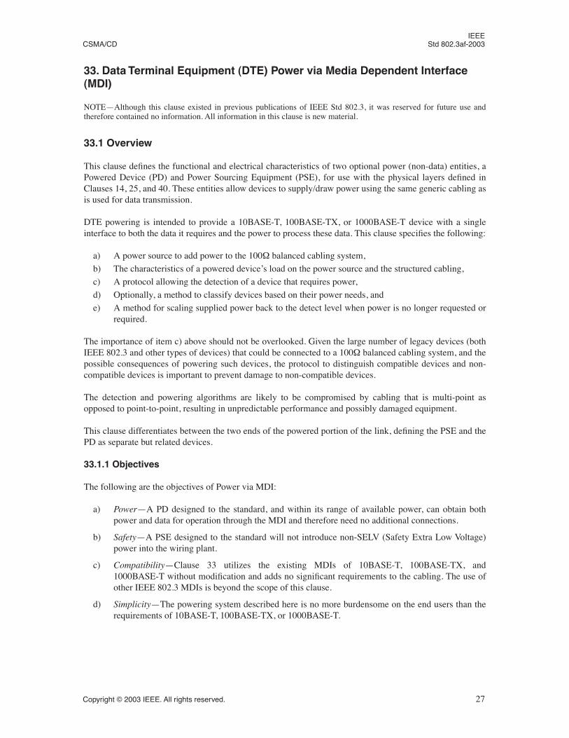
33. Data Terminal Equipment (DTE) Power via Media Dependent Interface (MDI)
NOTE—Although this clause existed in previous publications of IEEE Std 802.3, it was reserved for future use andtherefore contained no information. All information in this clause is new material.
33.1 Overview
This clause defines the functional and electrical characteristics of two optional power (non-data) entities, aPowered Device (PD) and Power Sourcing Equipment (PSE), for use with the physical layers defined inClauses 14, 25, and 40. These entities allow devices to supply/draw power using the same generic cabling asis used for data transmission.
DTE powering is intended to provide a 10BASE-T, 100BASE-TX, or 1000BASE-T device with a singleinterface to both the data it requires and the power to process these data. This clause specifies the following:
a) A power source to add power to the 100Ω balanced cabling system,
b) The characteristics of a powered device’s load on the power source and the structured cabling,
c) A protocol allowing the detection of a device that requires power,
d) Optionally, a method to classify devices based on their power needs, and
e) A method for scaling supplied power back to the detect level when power is no longer requested orrequired.
The importance of item c) above should not be overlooked. Given the large number of legacy devices (bothIEEE 802.3 and other types of devices) that could be connected to a 100Ω balanced cabling system, and thepossible consequences of powering such devices, the protocol to distinguish compatible devices and non-compatible devices is important to prevent damage to non-compatible devices.
The detection and powering algorithms are likely to be compromised by cabling that is multi-point asopposed to point-to-point, resulting in unpredictable performance and possibly damaged equipment.
This clause differentiates between the two ends of the powered portion of the link, defining the PSE and thePD as separate but related devices.
33.1.1 Objectives
The following are the objectives of Power via MDI:
a) Power—A PD designed to the standard, and within its range of available power, can obtain bothpower and data for operation through the MDI and therefore need no additional connections.
b) Safety—A PSE designed to the standard will not introduce non-SELV (Safety Extra Low Voltage)power into the wiring plant.
c) Compatibility—Clause 33 utilizes the existing MDIs of 10BASE-T, 100BASE-TX, and1000BASE-T without modification and adds no significant requirements to the cabling. The use ofother IEEE 802.3 MDIs is beyond the scope of this clause.
d) Simplicity—The powering system described here is no more burdensome on the end users than therequirements of 10BASE-T, 100BASE-TX, or 1000BASE-T.
Copyright © 2003 IEEE. All rights reserved. 27
IEEE Std 802.3af-2003 AMENDMENT TO IEEE Std 802.3
33.1.2 Compatibility considerations
All implementations of PD and PSE systems shall be compatible at their respective Power Interfaces (PIs)when used in accordance with the restrictions of Clause 33 where appropriate. Designers are free to imple-ment circuitry within the PD and PSE in an application-dependent manner provided that the respective PIspecifications are satisfied.
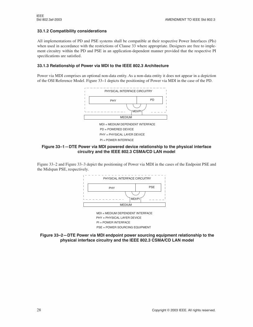
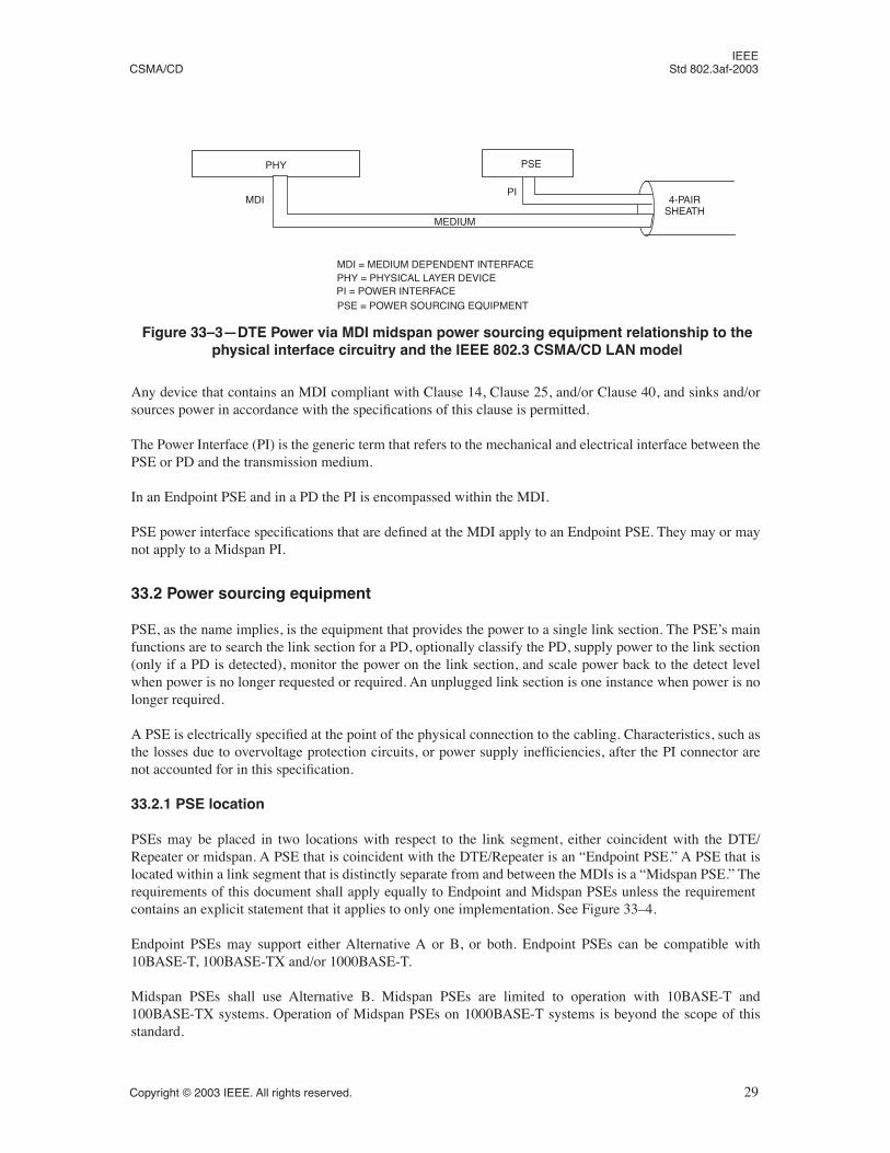
33.1.3 Relationship of Power via MDI to the IEEE 802.3 Architecture
Power via MDI comprises an optional non-data entity. As a non-data entity it does not appear in a depictionof the OSI Reference Model. Figure 33–1 depicts the positioning of Power via MDI in the case of the PD.
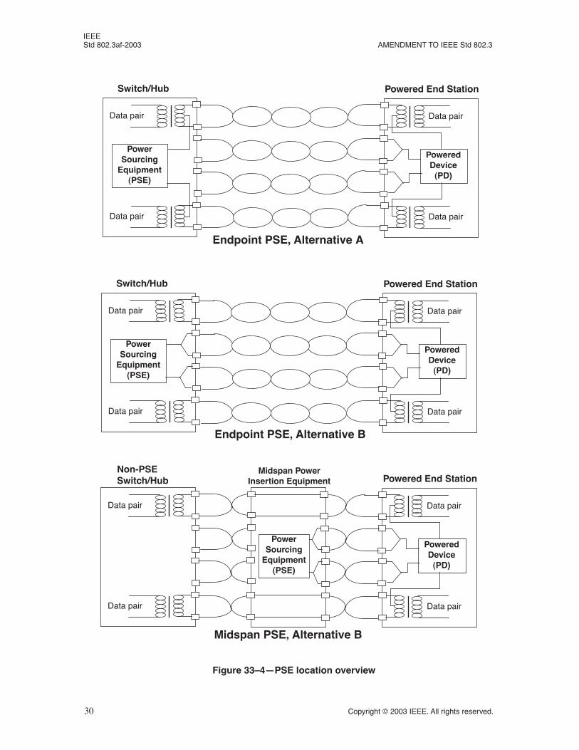
Figure 33–2 and Figure 33–3 depict the positioning of Power via MDI in the cases of the Endpoint PSE andthe Midspan PSE, respectively.
MDI/PI
MEDIUM
Figure 33–1—DTE Power via MDI powered device relationship to the physical interface circuitry and the IEEE 802.3 CSMA/CD LAN model
MDI = MEDIUM DEPENDENT INTERFACE
PHY = PHYSICAL LAYER DEVICE
PHY PD
PHYSICAL INTERFACE CIRCUITRY
PD = POWERED DEVICE
PI = POWER INTERFACE
Figure 33–2—DTE Power via MDI endpoint power sourcing equipment relationship to the physical interface circuitry and the IEEE 802.3 CSMA/CD LAN model
MDI/PI
MDI = MEDIUM DEPENDENT INTERFACE
PHY = PHYSICAL LAYER DEVICE
PHY PSE
PHYSICAL INTERFACE CIRCUITRY
MEDIUM
PSE = POWER SOURCING EQUIPMENT
PI = POWER INTERFACE
28 Copyright © 2003 IEEE. All rights reserved.
IEEE CSMA/CD Std 802.3af-2003
Any device that contains an MDI compliant with Clause 14, Clause 25, and/or Clause 40, and sinks and/orsources power in accordance with the specifications of this clause is permitted.
The Power Interface (PI) is the generic term that refers to the mechanical and electrical interface between thePSE or PD and the transmission medium.
In an Endpoint PSE and in a PD the PI is encompassed within the MDI.
PSE power interface specifications that are defined at the MDI apply to an Endpoint PSE. They may or maynot apply to a Midspan PI.
33.2 Power sourcing equipment
PSE, as the name implies, is the equipment that provides the power to a single link section. The PSE’s mainfunctions are to search the link section for a PD, optionally classify the PD, supply power to the link section(only if a PD is detected), monitor the power on the link section, and scale power back to the detect levelwhen power is no longer requested or required. An unplugged link section is one instance when power is nolonger required.
A PSE is electrically specified at the point of the physical connection to the cabling. Characteristics, such asthe losses due to overvoltage protection circuits, or power supply inefficiencies, after the PI connector arenot accounted for in this specification.
33.2.1 PSE location
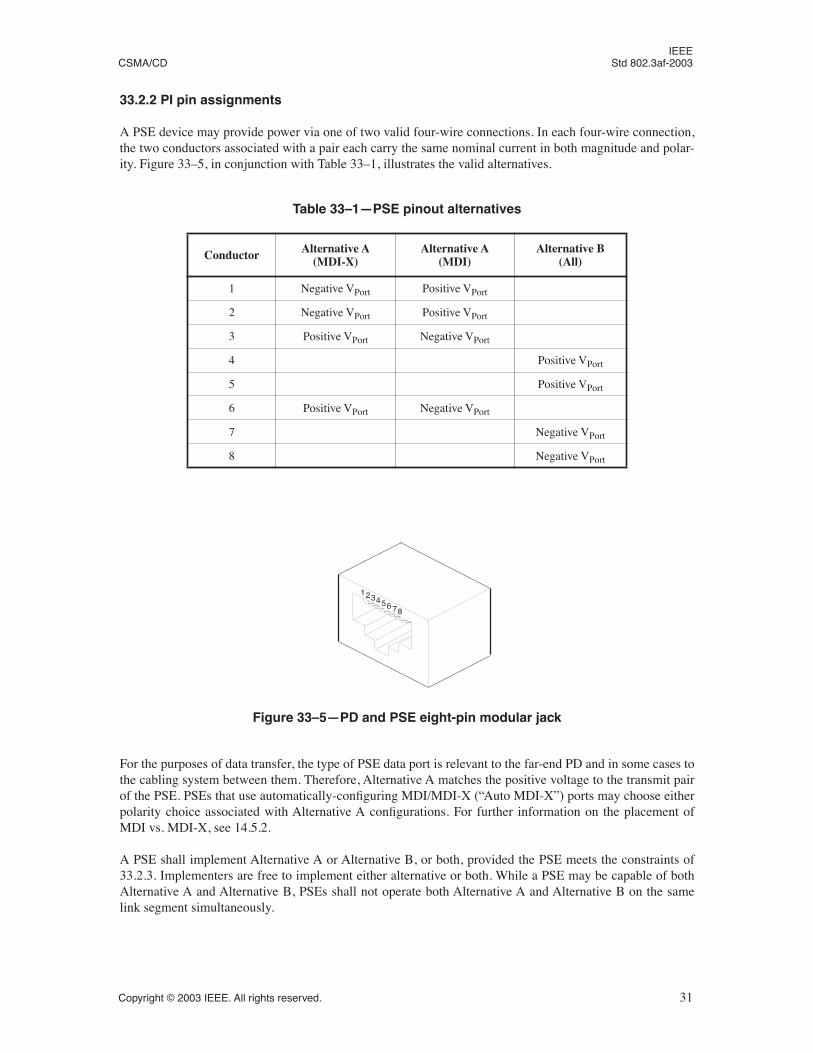
PSEs may be placed in two locations with respect to the link segment, either coincident with the DTE/Repeater or midspan. A PSE that is coincident with the DTE/Repeater is an “Endpoint PSE.” A PSE that islocated within a link segment that is distinctly separate from and between the MDIs is a “Midspan PSE.” Therequirements of this document shall apply equally to Endpoint and Midspan PSEs unless the requirementcontains an explicit statement that it applies to only one implementation. See Figure 33–4.
Endpoint PSEs may support either Alternative A or B, or both. Endpoint PSEs can be compatible with10BASE-T, 100BASE-TX and/or 1000BASE-T.
Midspan PSEs shall use Alternative B. Midspan PSEs are limited to operation with 10BASE-T and100BASE-TX systems. Operation of Midspan PSEs on 1000BASE-T systems is beyond the scope of thisstandard.
Figure 33–3—DTE Power via MDI midspan power sourcing equipment relationship to the physical interface circuitry and the IEEE 802.3 CSMA/CD LAN model
MDI
PHY PSE
4-PAIRSHEATH
PHY = PHYSICAL LAYER DEVICEMDI = MEDIUM DEPENDENT INTERFACE
PSE = POWER SOURCING EQUIPMENTPI = POWER INTERFACE
PI
MEDIUM
Copyright © 2003 IEEE. All rights reserved. 29
IEEE Std 802.3af-2003 AMENDMENT TO IEEE Std 802.3
Figure 33–4—PSE location overview
Data pair
Data pair
Endpoint PSE, Alternative A
Switch/Hub
Data pair
Data pair
Powered End Station
PowerSourcing
Equipment(PSE)
PoweredDevice
(PD)
Data pair
Data pair
Endpoint PSE, Alternative B
Switch/Hub
Data pair
Data pair
Powered End Station
PowerSourcing
Equipment(PSE)
PoweredDevice
(PD)
Data pair
Data pair
Midspan PSE, Alternative B
Non-PSESwitch/Hub
Data pair
Data pair
Powered End Station
PowerSourcing
Equipment(PSE)
PoweredDevice
(PD)
Midspan PowerInsertion Equipment
30 Copyright © 2003 IEEE. All rights reserved.
IEEE CSMA/CD Std 802.3af-2003
33.2.2 PI pin assignments
A PSE device may provide power via one of two valid four-wire connections. In each four-wire connection,the two conductors associated with a pair each carry the same nominal current in both magnitude and polar-ity. Figure 33–5, in conjunction with Table 33–1, illustrates the valid alternatives.
For the purposes of data transfer, the type of PSE data port is relevant to the far-end PD and in some cases tothe cabling system between them. Therefore, Alternative A matches the positive voltage to the transmit pairof the PSE. PSEs that use automatically-configuring MDI/MDI-X (“Auto MDI-X”) ports may choose eitherpolarity choice associated with Alternative A configurations. For further information on the placement ofMDI vs. MDI-X, see 14.5.2.
A PSE shall implement Alternative A or Alternative B, or both, provided the PSE meets the constraints of33.2.3. Implementers are free to implement either alternative or both. While a PSE may be capable of bothAlternative A and Alternative B, PSEs shall not operate both Alternative A and Alternative B on the samelink segment simultaneously.
Table 33–1—PSE pinout alternatives
Conductor Alternative A(MDI-X)
Alternative A(MDI)
Alternative B(All)
1 Negative VPort Positive VPort
2 Negative VPort Positive VPort
3 Positive VPort Negative VPort
4 Positive VPort
5 Positive VPort
6 Positive VPort Negative VPort
7 Negative VPort
8 Negative VPort
Figure 33–5—PD and PSE eight-pin modular jack
123456 78
Copyright © 2003 IEEE. All rights reserved. 31
IEEE Std 802.3af-2003 AMENDMENT TO IEEE Std 802.3
33.2.3 PSE state diagrams
The PSE state diagrams specify the externally observable behavior of a PSE. Equivalent implementationsthat present the same external behavior are allowed.
The PSE shall provide the behavior of the state diagrams shown in Figure 33–6 and Figure 33–7.
33.2.3.1 Overview
Detection, classification, and power turn-on timing shall meet the specifications in Table 33–5.
The PSE shall turn on power after a valid detection in less than Tpon as specified in Table 33–5, if power is tobe applied. If the PSE cannot supply power within Tpon, it shall initiate and successfully complete a newdetection cycle before applying power.
It is possible that two separate PSEs, one that implements Alternative A and one that implements AlternativeB (see 33.2.1), may be attached to the same link segment. In such a configuration, and without the requiredbackoff algorithm, the PSEs could prevent each other from ever detecting a PD by interfering with the detec-tion process of the other.
After a PSE that is performing detection using Alternative B fails to detect a valid PD detection signature,the PSE shall back off no less than Tdbo as specified in Table 33–5 before attempting another detection. Dur-ing this backoff, the PSE shall not apply a voltage greater than 2.8Vdc to the PI. A PSE that is performingAlternative B detection shall not resume detection mode until at least one backoff cycle has elapsed.
If a PSE that is performing detection using Alternative B detects an open circuit (see 33.2.6.3) on the linksection, then that PSE may optionally omit the detection backoff.
If a PSE performing detection using Alternative A detects an invalid signature, it should initiate a seconddetection attempt within 1 second after the beginning of the first detection attempt. This ensures that a PSEperforming detection using Alternative A will complete a second detection cycle prior to a PSE using Alter-native B that might also be present on the same Link Section, and therefore causing the invalid signature,completing its second detection cycle due to the Alternative B detection backoff described above.
33.2.3.2 Conventions
The notation used in the state diagrams follows the conventions of state diagrams as described in 21.5.
33.2.3.3 Constants
The PSE state diagrams use the following constants:
ICUT
Overload current detection range (see Table 33–5)ILIM
Output current at short circuit condition (see Table 33–5)IInrush
Current during inrush period of startup (see Table 33–5)
33.2.3.4 Variables
The PSE state diagrams use the following variables:
32 Copyright © 2003 IEEE. All rights reserved.
IEEE CSMA/CD Std 802.3af-2003
error_conditionA variable indicating the status of implementation-specific fault conditions that require the PSE notto source power. These error conditions are not the same conditions monitored by the state dia-grams in Figure 33–7.Values: FALSE: No fault indication.
TRUE: A fault indication exists.mr_mps_valid
The PSE monitors either the DC or AC Maintain Power Signature (MPS, see 33.2.10.1). This vari-able indicates the presence or absence of a valid MPS.Values: FALSE: If monitoring both components of the MPS, when the DC component of MPS
is absent or the AC component of MPS is absent. If monitoring only one com-ponent of MPS, that component of MPS is absent.
TRUE: If monitoring both components of the MPS, the DC component of MPS andthe AC component of MPS are both present. If monitoring only one compo-nent of MPS, that component of MPS is present.
mr_pse_alternativeThis variable indicates which pinout alternative the PSE will use to apply power to the link (seeTable 33–1). This variable is provided by a management interface that may be mapped to the PSEControl register Pair Control bits (11.3:2) or other equivalent function.Values: A: The PSE uses PSE pinout Alternative A.
B: The PSE uses PSE pinout Alternative B.mr_pse_enable
A control variable that selects PSE operation and test functions. This variables is provided by amanagement interface that may be mapped to the PSE Control register PSE Enable bits (11.1:0), asdescribed below, or other equivalent function.Values: disable: All PSE functions disabled (behavior is as if there was no PSE functionality).
This value corresponds to MDIO register bits 11.1:0 = '00'.enable: Normal PSE operation. This value corresponds to MDIO register bits 11.1:0 =
'01'.force_power:Test mode selected that causes the PSE to apply power to the PI when there
are no detected error conditions. This value corresponds to MDIO register bits11.1:0 = '10'.
performs_classificationThe performance of optional classification by the PSE is indicated by performs_classification.Values: FALSE: The PSE does not perform classification.
TRUE: The PSE does perform classification.pi_powered
A variable that controls the circuitry that the PSE uses to power the PD.Values: FALSE: The PSE is not to apply power to the link (default).
TRUE: The PSE has detected a PD, optionally classified it, and determined the PDwill be powered.
power_appliedA variable indicating that the PSE has begun steady state operation by having asserted pi_powered,completed the ramp of power per TRise of Table 33–5 and is operating beyond the startup require-ments of 33.2.8.5.Values: FALSE: The PSE is either not applying power or has begun applying power but is still
in startup.TRUE: The PSE has begun steady state operation.
pse_available_powerThis variable indicates the highest power PD Class that could be supported. The value is deter-mined in an implementation-specific manner.Values: 0: Class 1
1: Class 22: Class 0, Class 3 and Class 4
Copyright © 2003 IEEE. All rights reserved. 33
IEEE Std 802.3af-2003 AMENDMENT TO IEEE Std 802.3
power_not_availableVariable that is asserted in an implementation-dependent manner when the PSE is no longer capa-ble of sourcing sufficient power to support the PD Class of the attached PD.Values: FALSE: PSE is capable to continue to source power to a PD.
TRUE: PSE is no longer capable of sourcing power to a PD.pse_ready
Variable that is asserted in an implementation-dependent manner to probe the link segment.Values: FALSE: PSE is not ready to probe the link segment.
TRUE: PSE is ready to probe the link segment.
NOTE—Care should be taken when negating this variable in a PSE performing detection using Alternative A after aninvalid signature is detected due to the delay it will introduce between detection attempts (see 33.2.3.1).
pse_resetControls the resetting of the PSE state diagram. Condition that is TRUE until such time as thepower supply for the device that contains the PSE overall state diagrams has reached the operatingregion. It is also TRUE when implementation specific reasons require reset of PSE functionality.Values: FALSE: Do not reset the PSE state diagram.
TRUE: Reset the PSE state diagram.
33.2.3.5 Timers
All timers operate in the manner described in 14.2.3.2 with the following addition. A timer is reset and stopscounting upon entering a state where “stop x_timer” is asserted.
tdbo_timerA timer used to regulate backoff upon detection of an invalid signature, see Tdbo in Table 33–5.
tdet_timerA timer used to limit an attempt to detect a PD, see Tdet in Table 33–5.
ted_timerA timer used to regulate a subsequent attempt to detect a PD after an error condition causes powerremoval, see Ted in Table 33–5.
tlim_timerA timer used to monitor the duration of a short-circuit condition, see TLIM in Table 33–5.
tovld_timerA timer used to monitor the duration of an overcurrent condition, see Tovld in Table 33–5.
tmpdo_timerA timer used to monitor the dropout of the MPS, see TMPDO in Table 33–5.
tpon_timerA timer used to limit the time for power turn-on, see Tpon in Table 33–5.
tpdc_timerA timer used to limit the classification time, see Tpdc in Table 33–5.
33.2.3.6 Functions
do_detectionThis function returns multiple variables: The variable signature as defined in 33.2.6 and the variable mr_valid_siganture.signature: This variable indicates the presence or absence of a PD.Values: open_circuit: The PSE has detected an open circuit. This value is optionally returned
by a PSE performing detection using Alternative B.valid: The PSE has detected a PD requesting power.invalid: Neither open_circuit, nor valid PD detection signature has been found.
34 Copyright © 2003 IEEE. All rights reserved.
IEEE CSMA/CD Std 802.3af-2003
mr_valid_signature: This variable indicates that the PSE has detected a valid signature.Values: FALSE: No valid signature detected.
TRUE: Valid signature detected.do_classification
This function returns multiple variables: pd_requested_power: This variable indicates the power class requested by the PD.Values: 0: Class 1
1: Class 22: Class 0, Class 3 or Class 4
mr_pd_class_detected: The class of the PD associated with the PD detection signature, seeTable 33–3, 33.2.7. Class 0 is returned if an invalid classification signature is detected.Values: Class_0
Class_1Class_2Class_3Class_4
Copyright © 2003 IEEE. All rights reserved. 35
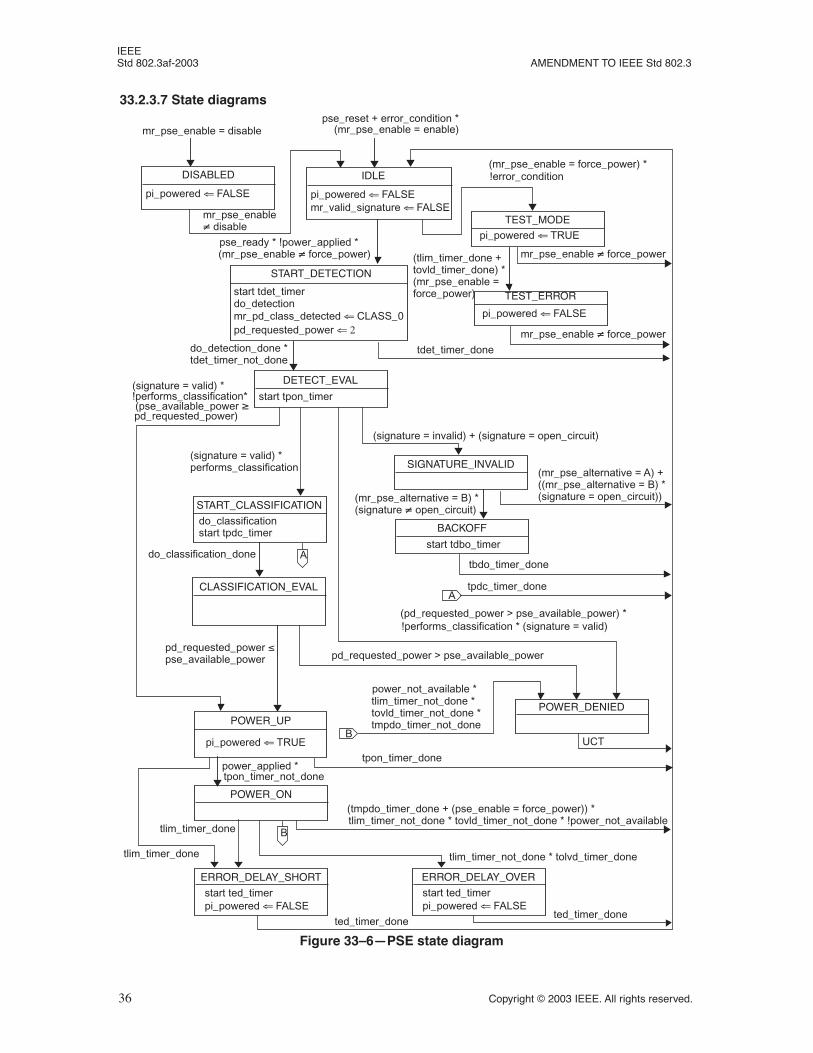
IEEE Std 802.3af-2003 AMENDMENT TO IEEE Std 802.3
33.2.3.7 State diagramspse_reset + error_condition *
IDLE
pi_powered ⇐ FALSE
START_DETECTION
start tdet_timer
mr_pd_class_detected ⇐ CLASS_0
(pd_requested_power > pse_available_power) *
SIGNATURE_INVALID
BACKOFF
start tdbo_timer
START_CLASSIFICATION
do_classificationstart tpdc_timer
(mr_pse_alternative = B) *
tbdo_timer_done
pd_requested_power > pse_available_power
(signature = invalid) + (signature = open_circuit)
(signature = valid) *!performs_classification*
pd_requested_power ≤pse_available_power
(mr_pse_alternative = A) +((mr_pse_alternative = B) * (signature = open_circuit))
(signature = valid) *performs_classification
TEST_MODE
pi_powered ⇐ TRUE
(mr_pse_enable = force_power) *!error_condition
mr_pse_enable ≠ force_power
mr_pse_enable ≠ force_power
(tlim_timer_done +
TEST_ERROR
pi_powered ⇐ FALSE
pse_ready * !power_applied *
DETECT_EVAL
do_detection_done *
start tpon_timer
!performs_classification * (signature = valid)
CLASSIFICATION_EVAL
do_classification_done
POWER_UP
pi_powered ⇐ TRUEtpon_timer_done
power_applied *
POWER_ON
tlim_timer_done
ERROR_DELAY_SHORT
start ted_timer
ted_timer_done
(tmpdo_timer_done + (pse_enable = force_power)) *
POWER_DENIED
UCT
do_detection
pd_requested_power ⇐ 2
tpdc_timer_done
tdet_timer_done
(signature ≠ open_circuit)
DISABLED
pi_powered ⇐ FALSE
mr_pse_enable
mr_pse_enable = disable
≠ disable
(mr_pse_enable = enable)
tovld_timer_done) *
A
A
Figure 33–6—PSE state diagram
mr_valid_signature ⇐ FALSE
pi_powered ⇐ FALSE
tlim_timer_not_done * tolvd_timer_done
ERROR_DELAY_OVER
start ted_timerpi_powered ⇐ FALSE
ted_timer_done
tlim_timer_done
(pse_available_power ≥pd_requested_power)
(mr_pse_enable ≠ force_power)
(mr_pse_enable =force_power)
tdet_timer_not_done
tpon_timer_not_done
tlim_timer_not_done * tovld_timer_not_done * !power_not_availableB
power_not_available *tlim_timer_not_done *tovld_timer_not_done *tmpdo_timer_not_done
B
36 Copyright © 2003 IEEE. All rights reserved.
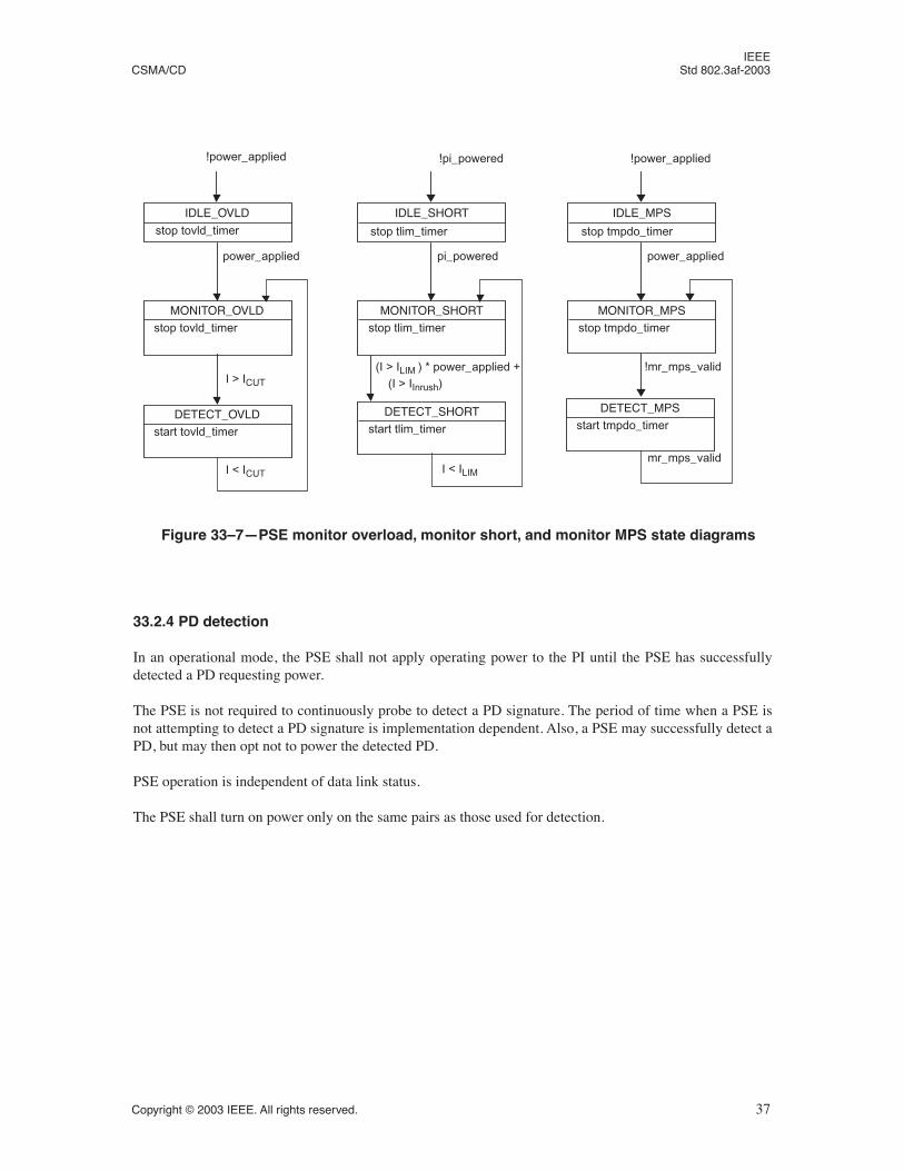
IEEE CSMA/CD Std 802.3af-2003
33.2.4 PD detection
In an operational mode, the PSE shall not apply operating power to the PI until the PSE has successfullydetected a PD requesting power.
The PSE is not required to continuously probe to detect a PD signature. The period of time when a PSE isnot attempting to detect a PD signature is implementation dependent. Also, a PSE may successfully detect aPD, but may then opt not to power the detected PD.
PSE operation is independent of data link status.
The PSE shall turn on power only on the same pairs as those used for detection.
!power_applied
power_applied
IDLE_OVLD
I > ICUT
MONITOR_OVLD
I < ICUT
DETECT_OVLD
stop tovld_timer
start tovld_timer
!pi_powered
pi_powered
IDLE_SHORT
(I > ILIM ) * power_applied +
MONITOR_SHORT
I < ILIM
DETECT_SHORT
stop tlim_timer
start tlim_timer
!power_applied
power_applied
IDLE_MPS
!mr_mps_valid
MONITOR_MPS
mr_mps_valid
DETECT_MPS
stop tmpdo_timer
start tmpdo_timer
Figure 33–7—PSE monitor overload, monitor short, and monitor MPS state diagrams
(I > IInrush)
stop tovld_timer stop tlim_timer stop tmpdo_timer
Copyright © 2003 IEEE. All rights reserved. 37
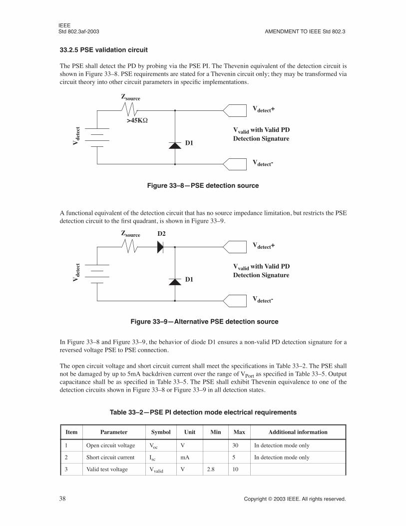
IEEE Std 802.3af-2003 AMENDMENT TO IEEE Std 802.3
33.2.5 PSE validation circuit
The PSE shall detect the PD by probing via the PSE PI. The Thevenin equivalent of the detection circuit isshown in Figure 33–8. PSE requirements are stated for a Thevenin circuit only; they may be transformed viacircuit theory into other circuit parameters in specific implementations.
A functional equivalent of the detection circuit that has no source impedance limitation, but restricts the PSEdetection circuit to the first quadrant, is shown in Figure 33–9.
In Figure 33–8 and Figure 33–9, the behavior of diode D1 ensures a non-valid PD detection signature for areversed voltage PSE to PSE connection.
The open circuit voltage and short circuit current shall meet the specifications in Table 33–2. The PSE shallnot be damaged by up to 5mA backdriven current over the range of VPort as specified in Table 33–5. Outputcapacitance shall be as specified in Table 33–5. The PSE shall exhibit Thevenin equivalence to one of thedetection circuits shown in Figure 33–8 or Figure 33–9 in all detection states.
Table 33–2—PSE PI detection mode electrical requirements
Item Parameter Symbol Unit Min Max Additional information
1 Open circuit voltage Voc V 30 In detection mode only
2 Short circuit current Isc mA 5 In detection mode only
3 Valid test voltage Vvalid V 2.8 10
Vdetect+
Vdetect-
Zsource
>45KΩ
Vde
tect
D1
Vvalid with Valid PD
Figure 33–8—PSE detection source
Detection Signature
Vdetect+
Vdetect-
Zsource
Vde
tect
D1
D2
Vvalid with Valid PD
Figure 33–9—Alternative PSE detection source
Detection Signature
38 Copyright © 2003 IEEE. All rights reserved.
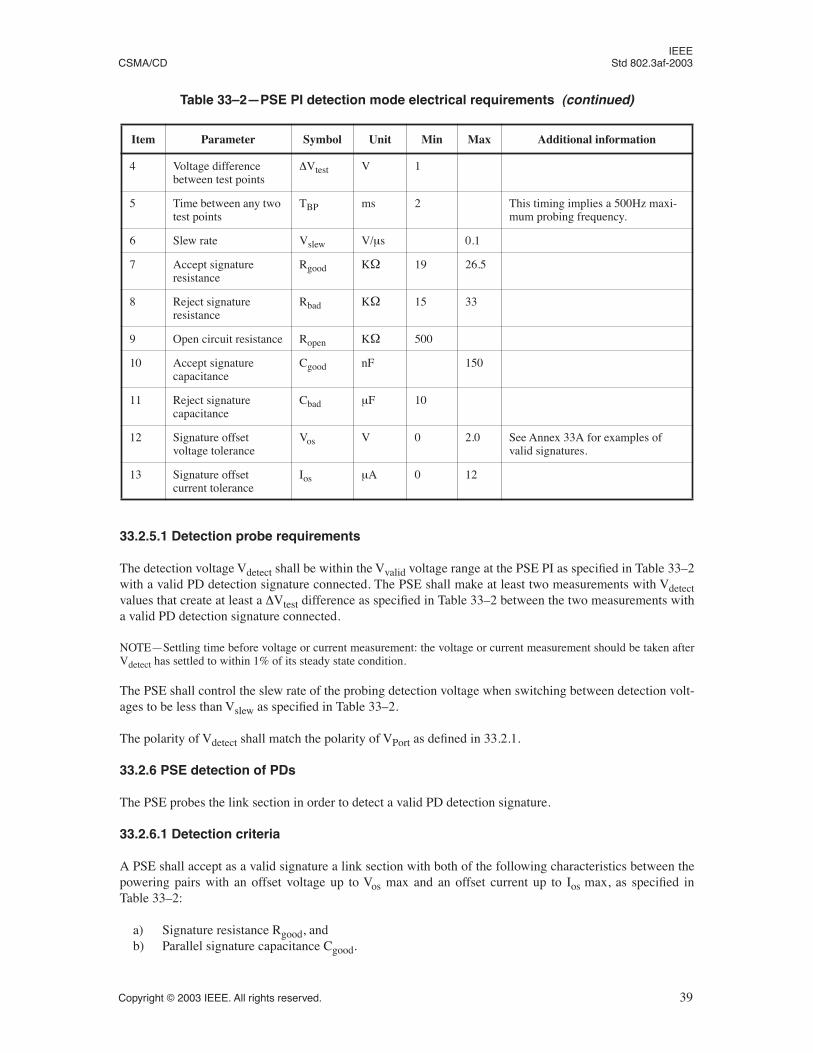
IEEE
CSMA/CD Std 802.3af-2003
33.2.5.1 Detection probe requirements
The detection voltage Vdetect shall be within the Vvalid voltage range at the PSE PI as specified in Table 33–2with a valid PD detection signature connected. The PSE shall make at least two measurements with Vdetectvalues that create at least a ∆Vtest difference as specified in Table 33–2 between the two measurements witha valid PD detection signature connected.
NOTE—Settling time before voltage or current measurement: the voltage or current measurement should be taken afterVdetect has settled to within 1% of its steady state condition.
The PSE shall control the slew rate of the probing detection voltage when switching between detection volt-ages to be less than Vslew as specified in Table 33–2.
The polarity of Vdetect shall match the polarity of VPort as defined in 33.2.1.
33.2.6 PSE detection of PDs
The PSE probes the link section in order to detect a valid PD detection signature.
33.2.6.1 Detection criteria
A PSE shall accept as a valid signature a link section with both of the following characteristics between thepowering pairs with an offset voltage up to Vos max and an offset current up to Ios max, as specified inTable 33–2:
a) Signature resistance Rgood, andb) Parallel signature capacitance Cgood.
4 Voltage difference between test points
∆Vtest V 1
5 Time between any two test points
TBP ms 2 This timing implies a 500Hz maxi-mum probing frequency.
6 Slew rate Vslew V/µs 0.1
7 Accept signature resistance
Rgood KΩ 19 26.5
8 Reject signature resistance
Rbad KΩ 15 33
9 Open circuit resistance Ropen KΩ 500
10 Accept signature capacitance
Cgood nF 150
11 Reject signature capacitance
Cbad µF 10
12 Signature offset voltage tolerance
Vos V 0 2.0 See Annex 33A for examples of valid signatures.
13 Signature offsetcurrent tolerance
Ios µA 0 12
Table 33–2—PSE PI detection mode electrical requirements (continued)
Item Parameter Symbol Unit Min Max Additional information
Copyright © 2003 IEEE. All rights reserved. 39
IEEE Std 802.3af-2003 AMENDMENT TO IEEE Std 802.3
NOTE—Caution, in a multiport system, the implementer should maintain DC isolation through the termination circuitryto eliminate cross-port leakage currents.
33.2.6.2 Rejection criteria
The PSE shall reject link sections as having an invalid signature, when those link sections exhibit any of thefollowing characteristics between the powering pairs, as specified in Table 33–2:
a) Resistance less than or equal to Rbad min, or
b) Resistance greater than or equal to Rbad max, or
c) Capacitance greater than or equal to Cbad min.
A PSE may accept or reject a signature resistance in the band between Rgood min and Rbad min, and in theband between Rgood max and Rbad max.
In instances where the resistance and capacitance meet the detection criteria, but one or both of the offset tol-erances are exceeded, the detection behavior of the PSE is undefined.
33.2.6.3 Open circuit criteria
If a PSE that is performing detection using Alternative B (see 33.2.2) determines that the impedance at the PIis greater than Ropen as defined in Table 33-2 item 9, then it may optionally consider the link to be open cir-cuit and omit the tdbo_timer interval.
33.2.7 PSE classification of PDs
The PSE may optionally classify a PD to allow features such as load management to be implemented. If aPSE successfully completes detection of a PD, and the PSE does not classify the PD in Class 1, 2, 3, or 4,then the PSE shall assign the PD to Class 0.
A successful classification of a PD requires:
a) Successful PD detection, and subsequently,b) Successful Class 0–4 classification.
A PSE may remove power to a PD that violates the maximum power required for its advertised class.
A PSE performs optional classification of a PD by applying voltage and measuring current, as specified in33.2.7.2. The PSE classification circuit should have adequate stability to prevent oscillation when connectedto a PD.
33.2.7.1 Classification power levels
PDs provide information that allow a PSE to classify their power requirements. The classifications are listedin Table 33–3.
Class 4 is reserved for future use. PDs classified as Class 4 shall be treated as Class 0 for powering purposes.
33.2.7.2 PSE classification
The PSE shall provide VClass between 15.5 and 20.5 volts, limited to 100 mA or less to the PI. Polarity shallbe the same as defined for VPort in 33.2.2 and timing specifications shall be as defined by Tpdc in Table 33–5.The PSE shall measure IClass and classify the PD based on the observed current according to Table 33–4. Ifthe measured IClass is equal to or greater than 51mA, the PSE shall classify the PD as Class 0.
40 Copyright © 2003 IEEE. All rights reserved.
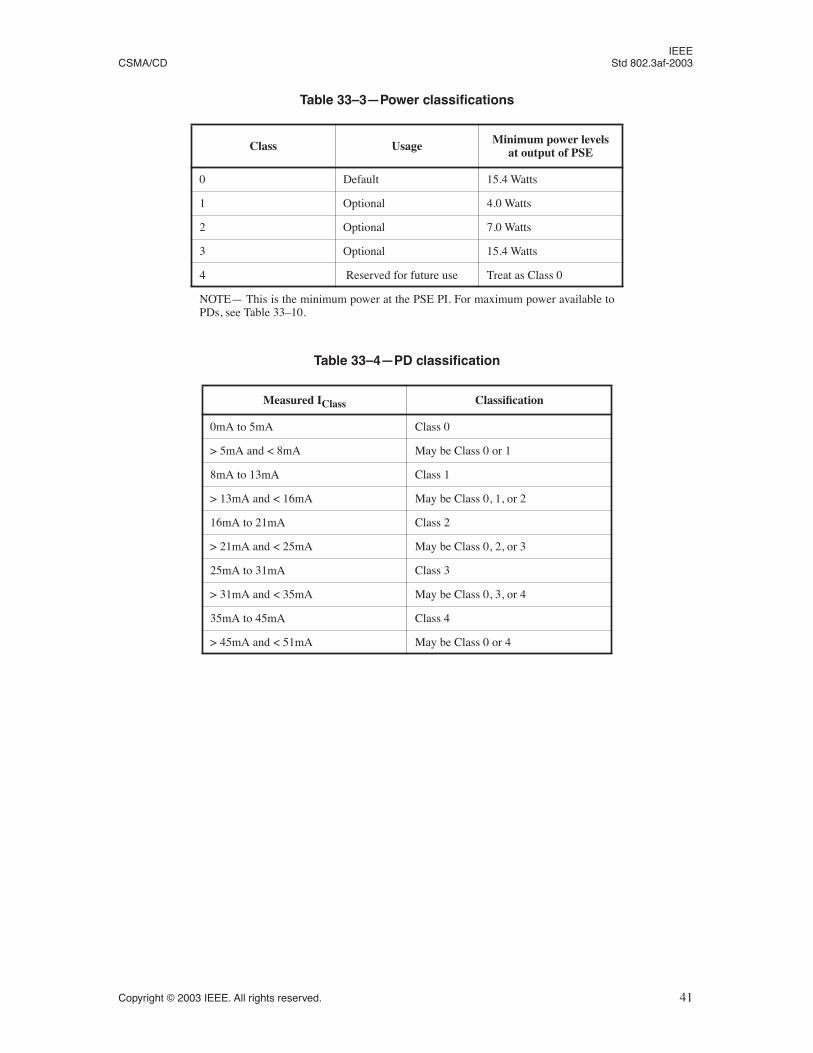
IEEE
CSMA/CD Std 802.3af-2003
Table 33–3—Power classifications
Class Usage Minimum power levels at output of PSE
0 Default 15.4 Watts
1 Optional 4.0 Watts
2 Optional 7.0 Watts
3 Optional 15.4 Watts
4 Reserved for future use Treat as Class 0
NOTE— This is the minimum power at the PSE PI. For maximum power available toPDs, see Table 33–10.
Table 33–4—PD classification
Measured IClass Classification
0mA to 5mA Class 0
> 5mA and < 8mA May be Class 0 or 1
8mA to 13mA Class 1
> 13mA and < 16mA May be Class 0, 1, or 2
16mA to 21mA Class 2
> 21mA and < 25mA May be Class 0, 2, or 3
25mA to 31mA Class 3
> 31mA and < 35mA May be Class 0, 3, or 4
35mA to 45mA Class 4
> 45mA and < 51mA May be Class 0 or 4
Copyright © 2003 IEEE. All rights reserved. 41
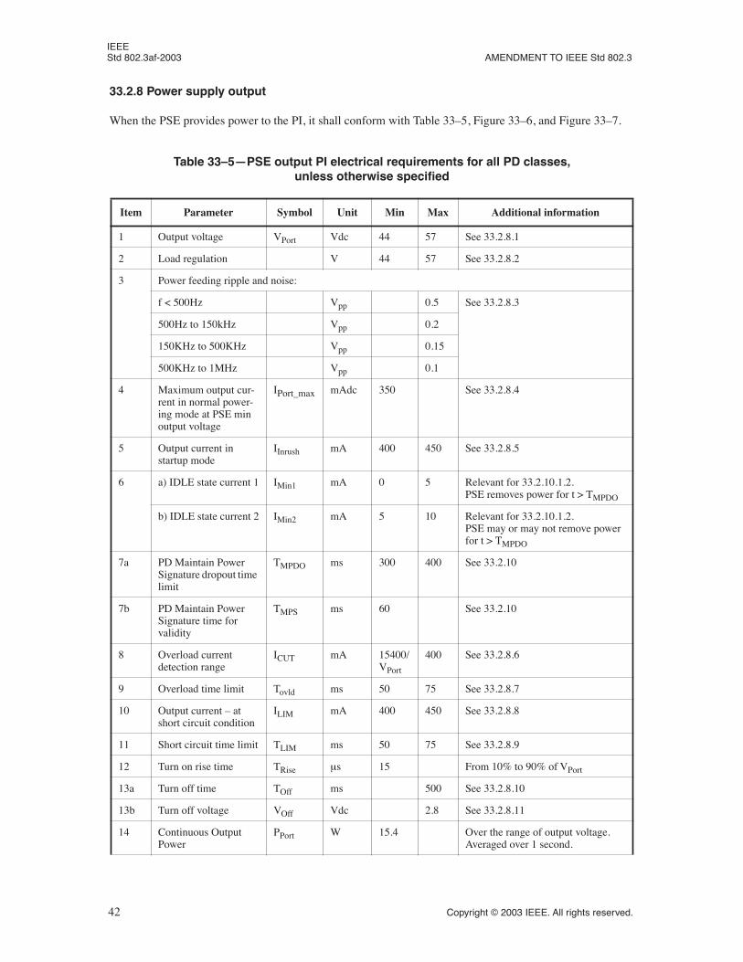
IEEE Std 802.3af-2003 AMENDMENT TO IEEE Std 802.3
33.2.8 Power supply output
When the PSE provides power to the PI, it shall conform with Table 33–5, Figure 33–6, and Figure 33–7.
Table 33–5—PSE output PI electrical requirements for all PD classes,unless otherwise specified
Item Parameter Symbol Unit Min Max Additional information
1 Output voltage VPort Vdc 44 57 See 33.2.8.1
2 Load regulation V 44 57 See 33.2.8.2
3 Power feeding ripple and noise:
f < 500Hz Vpp 0.5 See 33.2.8.3
500Hz to 150kHz Vpp 0.2
150KHz to 500KHz Vpp 0.15
500KHz to 1MHz Vpp 0.1
4 Maximum output cur-rent in normal power-ing mode at PSE min output voltage
IPort_max mAdc 350 See 33.2.8.4
5 Output current instartup mode
IInrush mA 400 450 See 33.2.8.5
6 a) IDLE state current 1 IMin1 mA 0 5 Relevant for 33.2.10.1.2.PSE removes power for t > TMPDO
b) IDLE state current 2 IMin2 mA 5 10 Relevant for 33.2.10.1.2.PSE may or may not remove power for t > TMPDO
7a PD Maintain Power Signature dropout time limit
TMPDO ms 300 400 See 33.2.10
7b PD Maintain Power Signature time for validity
TMPS ms 60 See 33.2.10
8 Overload current detection range
ICUT mA 15400/VPort
400 See 33.2.8.6
9 Overload time limit Tovld ms 50 75 See 33.2.8.7
10 Output current – at short circuit condition
ILIM mA 400 450 See 33.2.8.8
11 Short circuit time limit TLIM ms 50 75 See 33.2.8.9
12 Turn on rise time TRise µs 15 From 10% to 90% of VPort
13a Turn off time TOff ms 500 See 33.2.8.10
13b Turn off voltage VOff Vdc 2.8 See 33.2.8.11
14 Continuous Output Power
PPort W 15.4 Over the range of output voltage. Averaged over 1 second.
42 Copyright © 2003 IEEE. All rights reserved.
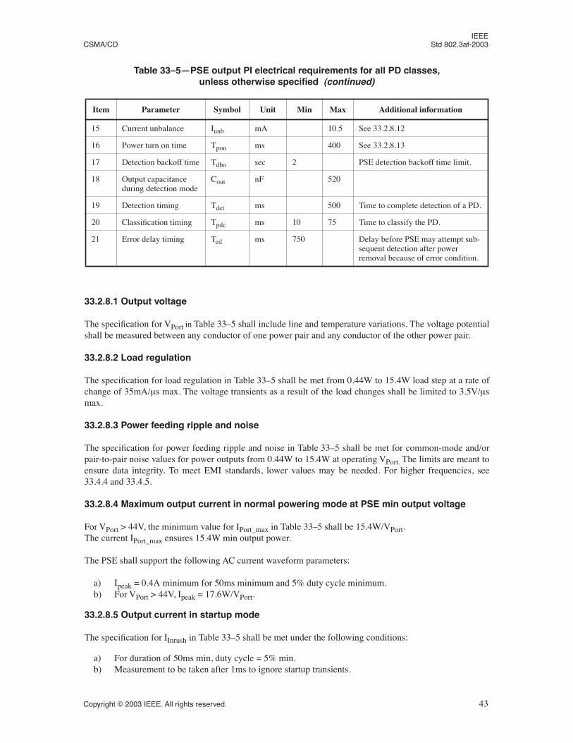
IEEE
CSMA/CD Std 802.3af-2003
33.2.8.1 Output voltage
The specification for VPort in Table 33–5 shall include line and temperature variations. The voltage potentialshall be measured between any conductor of one power pair and any conductor of the other power pair.
33.2.8.2 Load regulation
The specification for load regulation in Table 33–5 shall be met from 0.44W to 15.4W load step at a rate ofchange of 35mA/µs max. The voltage transients as a result of the load changes shall be limited to 3.5V/µsmax.
33.2.8.3 Power feeding ripple and noise
The specification for power feeding ripple and noise in Table 33–5 shall be met for common-mode and/orpair-to-pair noise values for power outputs from 0.44W to 15.4W at operating VPort. The limits are meant toensure data integrity. To meet EMI standards, lower values may be needed. For higher frequencies, see33.4.4 and 33.4.5.
33.2.8.4 Maximum output current in normal powering mode at PSE min output voltage
For VPort > 44V, the minimum value for IPort_max in Table 33–5 shall be 15.4W/VPort. The current IPort_max ensures 15.4W min output power.
The PSE shall support the following AC current waveform parameters:
a) Ipeak = 0.4A minimum for 50ms minimum and 5% duty cycle minimum.b) For VPort > 44V, Ipeak = 17.6W/VPort.
33.2.8.5 Output current in startup mode
The specification for IInrush in Table 33–5 shall be met under the following conditions:
a) For duration of 50ms min, duty cycle = 5% min.b) Measurement to be taken after 1ms to ignore startup transients.
15 Current unbalance Iunb mA 10.5 See 33.2.8.12
16 Power turn on time Tpon ms 400 See 33.2.8.13
17 Detection backoff time Tdbo sec 2 PSE detection backoff time limit.
18 Output capacitance during detection mode
Cout nF 520
19 Detection timing Tdet ms 500 Time to complete detection of a PD.
20 Classification timing Tpdc ms 10 75 Time to classify the PD.
21 Error delay timing Ted ms 750 Delay before PSE may attempt sub-sequent detection after power removal because of error condition.
Table 33–5—PSE output PI electrical requirements for all PD classes,unless otherwise specified (continued)
Item Parameter Symbol Unit Min Max Additional information
Copyright © 2003 IEEE. All rights reserved. 43
IEEE Std 802.3af-2003 AMENDMENT TO IEEE Std 802.3
c) During startup, the minimum IInrush requirement applies for duration TLIM.d) During startup, for PI voltages above 30V, the minimum IInrush requirement is as specified in
Table 33–5, item 5.e) During startup, for PI voltages between 10V and 30V, the minimum IInrush requirement is 60mA.
See Figure 33C.4 and Figure 33C.6.
33.2.8.6 Overload current detection range
If IPort in Table 33–5 exceeds ICUT for longer than Tovld, the PSE shall remove power from the PI. See Figure33C.6.
In a PSE that supports the optional classification function (33.2.7), the minimum value of ICUT may option-ally be
,
where P_class is the minimum power level at the output of the PSE (as specified by Table 33–3) and Vport-min is VPort min in Table 33–5.
33.2.8.7 Overload time limit
After time duration of Tovld as specified in Table 33–5, the PSE shall remove power from the PI. See Figure33C.6.
33.2.8.8 Output current—at short circuit condition
The power shall be removed from the PI within TLIM, as specified in Table 33–5, under the followingconditions:
a) Max value of the PI current during short circuit condition. b) Max value applies for any DC input voltage up to the maximum voltage as specified in item 1 of
Table 33–5.c) Measurement to be taken after 1ms to ignore initial transients.
See Figure 33C.4 and Figure 33C.6.
33.2.8.9 Short circuit time limit
If a short circuit condition is detected, power removal from the PI shall begin within TLIM and be completeby TOff, as specified in Table 33–5. See Figure 33C.4 and Figure 33C.6.
33.2.8.10 Turn off time
The specification for TOff in Table 33–5 shall apply to the discharge time from VPort to 2.8Vdc with a testresistor of 320KΩ attached to the PI. In addition, it is recommended that the PI be discharged when turnedoff. The PSE enters the IDLE state when VPort drops 1V below the steady-state value after the pi_poweredvariable is cleared (see Figure 33–6). The PSE remains in the IDLE state as long as the average voltageacross the PI is VOff. The IDLE State is the mode when the PSE is not in Detection, Classification, or normalpowering mode.
P_class 1000×( ) Vportmin⁄
44 Copyright © 2003 IEEE. All rights reserved.
IEEE CSMA/CD Std 802.3af-2003
33.2.8.11 Turn off voltage
The specification for VOff in Table 33–5 shall apply to the PI voltage in the IDLE State.
33.2.8.12 Current unbalance
The specification for Iunb in Table 33–5 shall apply to the current unbalance between the two conductors of apower pair over the current load range. The 10.5mA value is based on a simulated output current unbalanceof 3%.
33.2.8.13 Power turn on time
The specification for Tpon in Table 33–5 shall apply to the PSE power up time for a PD after completion ofdetection. If power is not applied as specified, a new detection cycle is initiated (See 33.2.3.1).
33.2.8.14 PSE stability
NOTE — Caution, when connected together as a system, the PSE and PD might exhibit instability at the PSE side or thePD side or both due to the presence of negative impedance at the PD input. See Annex 33D for PSE design guidelines toensure stable operation.
33.2.9 Power supply allocation
A PSE shall not initiate power provision to a link if the PSE is unable to provide the maximum power levelrequested by the PD based on the PD’s class. Where a PSE does not provide the optional classification func-tion specified in 33.2.7, all PDs are treated as Class 0.
The PSE may manage the allocation of power based on additional information beyond the classification ofthe attached PD. Allocating power based on additional information about the attached PD, and the mecha-nism for obtaining that additional information, is beyond the scope of this standard with the exception thatthe allocation of power shall not be based solely on the historical data of the power consumption of theattached PD.
If the system implements a power allocation algorithm, no additional behavioral requirement is placed onthe system as it approaches or reaches its maximum power subscription. Specifically, the interactionbetween one PSE PI and another PSE PI in the same system is beyond the scope of this standard.
33.2.10 PSE power removal
Figure 33–7 shows the PSE monitor state diagrams. These state diagrams monitor for overload current, shortcircuit, inrush current, and the absence of the Maintain Power Signature (MPS).
If any of these conditions exists for longer than its related time limit, the power will be removed from the PI.
33.2.10.1 PSE Maintain Power Signature (MPS) requirements
The MPS consists of two components, an AC MPS component and a DC MPS component.
The PSE may optionally monitor the AC MPS component only, the DC MPS component only or both the ACand the DC MPS components.
Copyright © 2003 IEEE. All rights reserved. 45
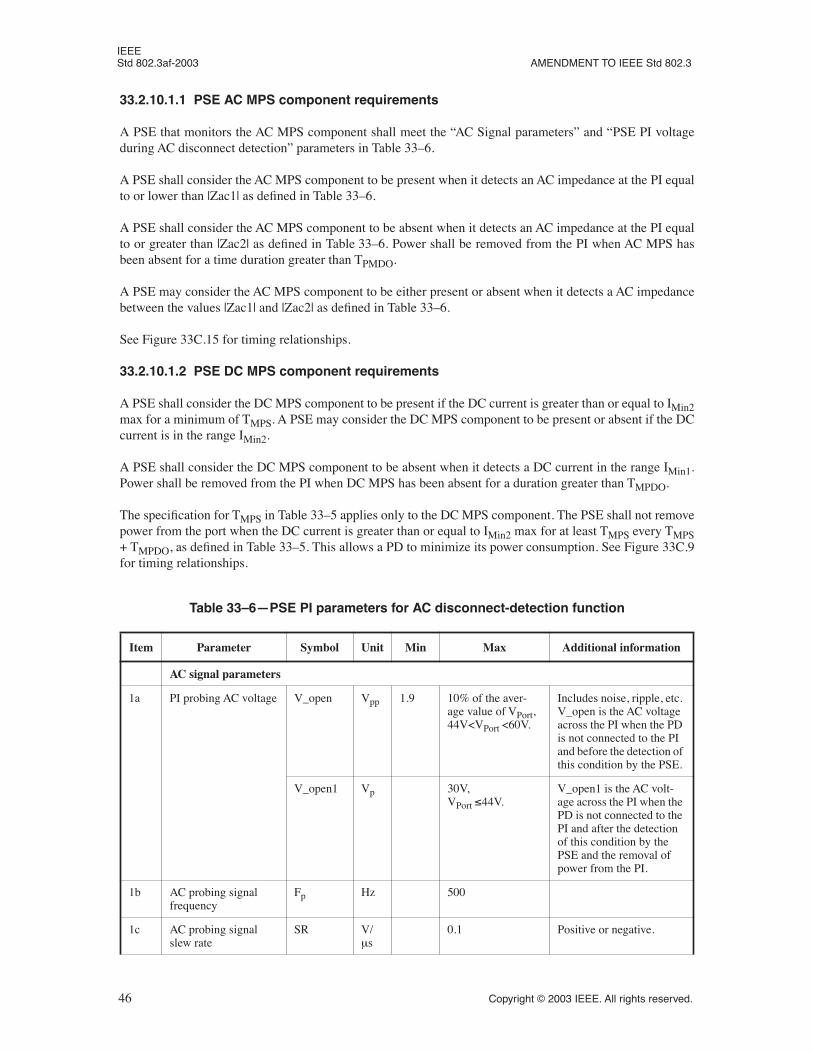
IEEE Std 802.3af-2003 AMENDMENT TO IEEE Std 802.3
33.2.10.1.1 PSE AC MPS component requirements
A PSE that monitors the AC MPS component shall meet the “AC Signal parameters” and “PSE PI voltageduring AC disconnect detection” parameters in Table 33–6.
A PSE shall consider the AC MPS component to be present when it detects an AC impedance at the PI equalto or lower than |Zac1| as defined in Table 33–6.
A PSE shall consider the AC MPS component to be absent when it detects an AC impedance at the PI equalto or greater than |Zac2| as defined in Table 33–6. Power shall be removed from the PI when AC MPS hasbeen absent for a time duration greater than TPMDO.
A PSE may consider the AC MPS component to be either present or absent when it detects a AC impedancebetween the values |Zac1| and |Zac2| as defined in Table 33–6.
See Figure 33C.15 for timing relationships.
33.2.10.1.2 PSE DC MPS component requirements
A PSE shall consider the DC MPS component to be present if the DC current is greater than or equal to IMin2max for a minimum of TMPS. A PSE may consider the DC MPS component to be present or absent if the DCcurrent is in the range IMin2.
A PSE shall consider the DC MPS component to be absent when it detects a DC current in the range IMin1.Power shall be removed from the PI when DC MPS has been absent for a duration greater than TMPDO.
The specification for TMPS in Table 33–5 applies only to the DC MPS component. The PSE shall not removepower from the port when the DC current is greater than or equal to IMin2 max for at least TMPS every TMPS+ TMPDO, as defined in Table 33–5. This allows a PD to minimize its power consumption. See Figure 33C.9for timing relationships.
Table 33–6—PSE PI parameters for AC disconnect-detection function
Item Parameter Symbol Unit Min Max Additional information
AC signal parameters
1a PI probing AC voltage V_open Vpp 1.9 10% of the aver-age value of VPort, 44V<VPort <60V.
Includes noise, ripple, etc. V_open is the AC voltage across the PI when the PD is not connected to the PI and before the detection of this condition by the PSE.
V_open1 Vp 30V,VPort ≤44V.
V_open1 is the AC volt-age across the PI when the PD is not connected to the PI and after the detection of this condition by the PSE and the removal of power from the PI.
1b AC probing signal frequency
Fp Hz 500
1c AC probing signal slew rate
SR V/µs
0.1 Positive or negative.
46 Copyright © 2003 IEEE. All rights reserved.
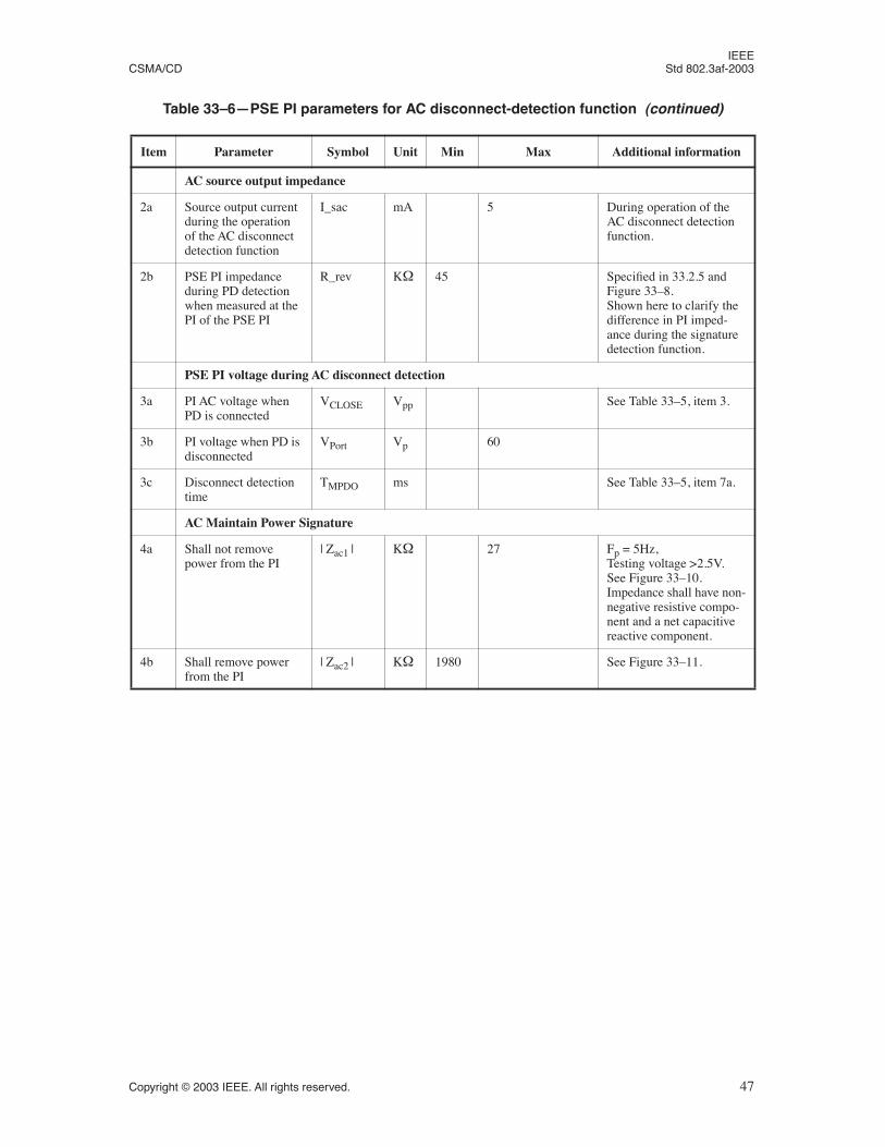
IEEE CSMA/CD Std 802.3af-2003
AC source output impedance
2a Source output current during the operation of the AC disconnect detection function
I_sac mA 5 During operation of the AC disconnect detection function.
2b PSE PI impedance during PD detection when measured at the PI of the PSE PI
R_rev KΩ 45 Specified in 33.2.5 and Figure 33–8.Shown here to clarify the difference in PI imped-ance during the signature detection function.
PSE PI voltage during AC disconnect detection
3a PI AC voltage when PD is connected
VCLOSE Vpp See Table 33–5, item 3.
3b PI voltage when PD is disconnected
VPort Vp 60
3c Disconnect detection time
TMPDO ms See Table 33–5, item 7a.
AC Maintain Power Signature
4a Shall not remove power from the PI
| Zac1 | KΩ 27 Fp = 5Hz, Testing voltage >2.5V.See Figure 33–10.Impedance shall have non-negative resistive compo-nent and a net capacitive reactive component.
4b Shall remove power from the PI
| Zac2 | KΩ 1980 See Figure 33–11.
Table 33–6—PSE PI parameters for AC disconnect-detection function (continued)
Item Parameter Symbol Unit Min Max Additional information
Copyright © 2003 IEEE. All rights reserved. 47
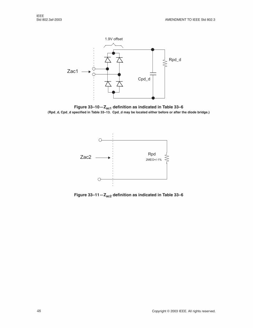
IEEE Std 802.3af-2003 AMENDMENT TO IEEE Std 802.3
Figure 33–10—Zac1 definition as indicated in Table 33–6(Rpd_d, Cpd_d specified in Table 33–13. Cpd_d may be located either before or after the diode bridge.)
Rpd_d
1.9V offset
Cpd_d
Zac1
Figure 33–11—Zac2 definition as indicated in Table 33–6
RpdZac2
2MEG+/-1%
48 Copyright © 2003 IEEE. All rights reserved.
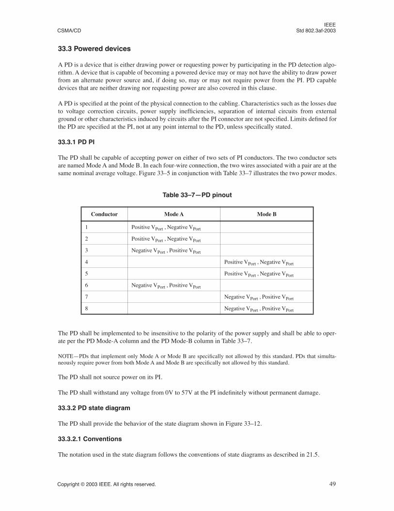
IEEE CSMA/CD Std 802.3af-2003
33.3 Powered devices
A PD is a device that is either drawing power or requesting power by participating in the PD detection algo-rithm. A device that is capable of becoming a powered device may or may not have the ability to draw powerfrom an alternate power source and, if doing so, may or may not require power from the PI. PD capabledevices that are neither drawing nor requesting power are also covered in this clause.
A PD is specified at the point of the physical connection to the cabling. Characteristics such as the losses dueto voltage correction circuits, power supply inefficiencies, separation of internal circuits from externalground or other characteristics induced by circuits after the PI connector are not specified. Limits defined forthe PD are specified at the PI, not at any point internal to the PD, unless specifically stated.
33.3.1 PD PI
The PD shall be capable of accepting power on either of two sets of PI conductors. The two conductor setsare named Mode A and Mode B. In each four-wire connection, the two wires associated with a pair are at thesame nominal average voltage. Figure 33–5 in conjunction with Table 33–7 illustrates the two power modes.
The PD shall be implemented to be insensitive to the polarity of the power supply and shall be able to oper-ate per the PD Mode-A column and the PD Mode-B column in Table 33–7.
NOTE—PDs that implement only Mode A or Mode B are specifically not allowed by this standard. PDs that simulta-neously require power from both Mode A and Mode B are specifically not allowed by this standard.
The PD shall not source power on its PI.
The PD shall withstand any voltage from 0V to 57V at the PI indefinitely without permanent damage.
33.3.2 PD state diagram
The PD shall provide the behavior of the state diagram shown in Figure 33–12.
33.3.2.1 Conventions
The notation used in the state diagram follows the conventions of state diagrams as described in 21.5.
Table 33–7—PD pinout
Conductor Mode A Mode B
1 Positive VPort , Negative VPort
2 Positive VPort , Negative VPort
3 Negative VPort , Positive VPort
4 Positive VPort , Negative VPort
5 Positive VPort , Negative VPort
6 Negative VPort , Positive VPort
7 Negative VPort , Positive VPort
8 Negative VPort , Positive VPort
Copyright © 2003 IEEE. All rights reserved. 49
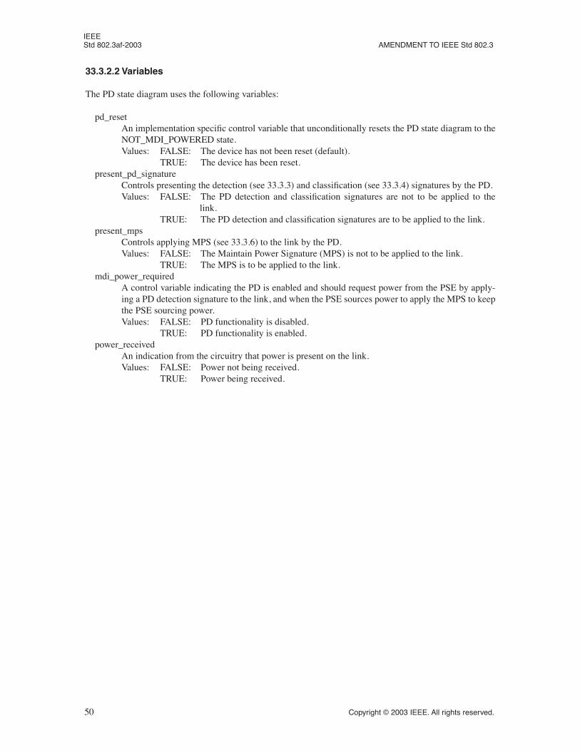
IEEE Std 802.3af-2003 AMENDMENT TO IEEE Std 802.3
33.3.2.2 Variables
The PD state diagram uses the following variables:
pd_resetAn implementation specific control variable that unconditionally resets the PD state diagram to theNOT_MDI_POWERED state.Values: FALSE: The device has not been reset (default).
TRUE: The device has been reset.present_pd_signature
Controls presenting the detection (see 33.3.3) and classification (see 33.3.4) signatures by the PD.Values: FALSE: The PD detection and classification signatures are not to be applied to the
link.TRUE: The PD detection and classification signatures are to be applied to the link.
present_mpsControls applying MPS (see 33.3.6) to the link by the PD.Values: FALSE: The Maintain Power Signature (MPS) is not to be applied to the link.
TRUE: The MPS is to be applied to the link.mdi_power_required
A control variable indicating the PD is enabled and should request power from the PSE by apply-ing a PD detection signature to the link, and when the PSE sources power to apply the MPS to keepthe PSE sourcing power.Values: FALSE: PD functionality is disabled.
TRUE: PD functionality is enabled.power_received
An indication from the circuitry that power is present on the link.Values: FALSE: Power not being received.
TRUE: Power being received.
50 Copyright © 2003 IEEE. All rights reserved.
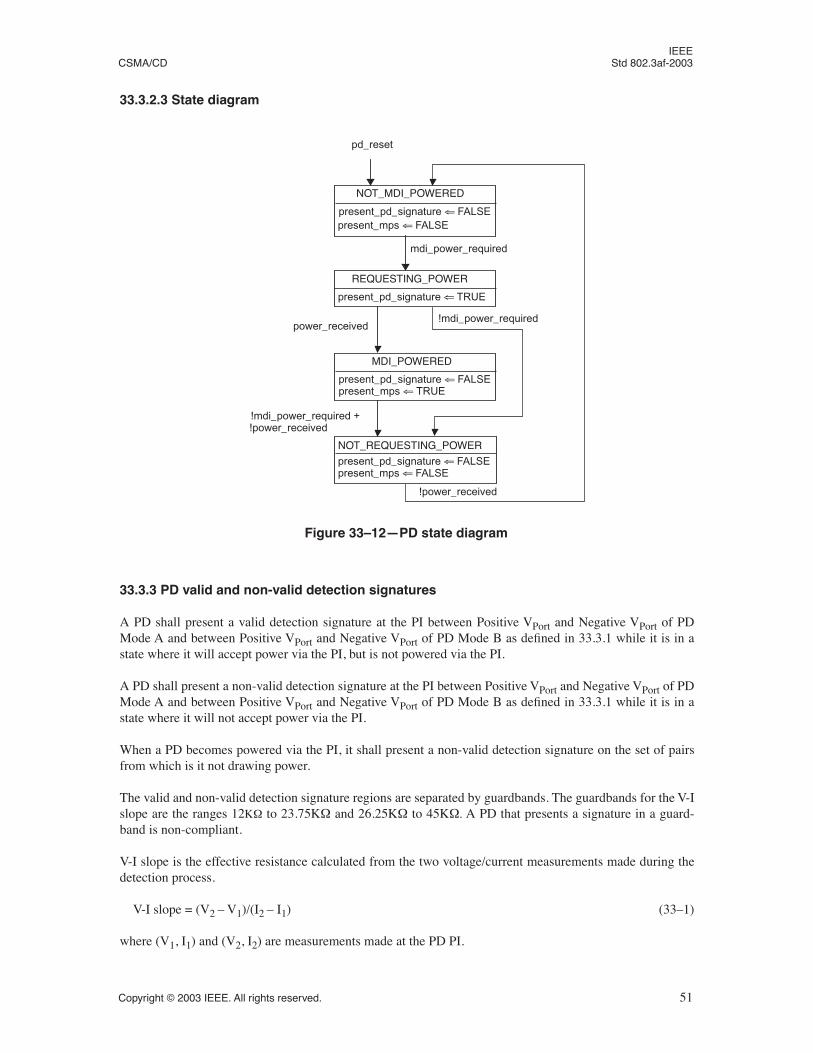
IEEE CSMA/CD Std 802.3af-2003
33.3.2.3 State diagram
33.3.3 PD valid and non-valid detection signatures
A PD shall present a valid detection signature at the PI between Positive VPort and Negative VPort of PDMode A and between Positive VPort and Negative VPort of PD Mode B as defined in 33.3.1 while it is in astate where it will accept power via the PI, but is not powered via the PI.
A PD shall present a non-valid detection signature at the PI between Positive VPort and Negative VPort of PDMode A and between Positive VPort and Negative VPort of PD Mode B as defined in 33.3.1 while it is in astate where it will not accept power via the PI.
When a PD becomes powered via the PI, it shall present a non-valid detection signature on the set of pairsfrom which is it not drawing power.
The valid and non-valid detection signature regions are separated by guardbands. The guardbands for the V-Islope are the ranges 12KΩ to 23.75KΩ and 26.25KΩ to 45KΩ. A PD that presents a signature in a guard-band is non-compliant.
V-I slope is the effective resistance calculated from the two voltage/current measurements made during thedetection process.
V-I slope = (V2 – V1)/(I2 – I1) (33–1)
where (V1, I1) and (V2, I2) are measurements made at the PD PI.
pd_reset
NOT_MDI_POWERED
present_pd_signature ⇐ FALSE
mdi_power_required
REQUESTING_POWER
present_pd_signature ⇐ TRUE
MDI_POWERED
present_pd_signature ⇐ FALSEpresent_mps ⇐ TRUE
NOT_REQUESTING_POWER
present_pd_signature ⇐ FALSEpresent_mps ⇐ FALSE
!mdi_power_requiredpower_received
!power_received
!mdi_power_required +!power_received
present_mps ⇐ FALSE
Figure 33–12—PD state diagram
Copyright © 2003 IEEE. All rights reserved. 51
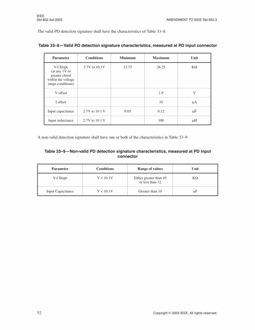
IEEE Std 802.3af-2003 AMENDMENT TO IEEE Std 802.3
The valid PD detection signature shall have the characteristics of Table 33–8.
A non-valid detection signature shall have one or both of the characteristics in Table 33–9
Table 33–8—Valid PD detection signature characteristics, measured at PD input connector
Parameter Conditions Minimum Maximum Unit
V-I Slope(at any 1V or greater chord
within the voltage range conditions)
2.7V to 10.1V 23.75 26.25 KΩ
V offset 1.9 V
I offset 10 µA
Input capacitance 2.7V to 10.1 V 0.05 0.12 µF
Input inductance 2.7V to 10.1 V 100 µH
Table 33–9—Non-valid PD detection signature characteristics, measured at PD input connector
Parameter Conditions Range of values Unit
V-I Slope V < 10.1V Either greater than 45or less than 12
KΩ
Input Capacitance V < 10.1V Greater than 10 µF
52 Copyright © 2003 IEEE. All rights reserved.
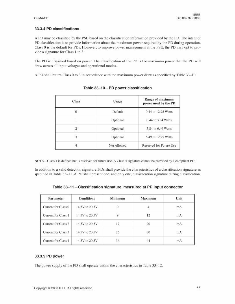
IEEE CSMA/CD Std 802.3af-2003
33.3.4 PD classifications
A PD may be classified by the PSE based on the classification information provided by the PD. The intent ofPD classification is to provide information about the maximum power required by the PD during operation.Class 0 is the default for PDs. However, to improve power management at the PSE, the PD may opt to pro-vide a signature for Class 1 to 3.
The PD is classified based on power. The classification of the PD is the maximum power that the PD willdraw across all input voltages and operational modes.
A PD shall return Class 0 to 3 in accordance with the maximum power draw as specified by Table 33–10.
NOTE—Class 4 is defined but is reserved for future use. A Class 4 signature cannot be provided by a compliant PD.
In addition to a valid detection signature, PDs shall provide the characteristics of a classification signature asspecified in Table 33–11. A PD shall present one, and only one, classification signature during classification.
33.3.5 PD power
The power supply of the PD shall operate within the characteristics in Table 33–12.
Table 33–10—PD power classification
Class Usage Range of maximum power used by the PD
0 Default 0.44 to 12.95 Watts
1 Optional 0.44 to 3.84 Watts
2 Optional 3.84 to 6.49 Watts
3 Optional 6.49 to 12.95 Watts
4 Not Allowed Reserved for Future Use
Table 33–11—Classification signature, measured at PD input connector
Parameter Conditions Minimum Maximum Unit
Current for Class 0 14.5V to 20.5V 0 4 mA
Current for Class 1 14.5V to 20.5V 9 12 mA
Current for Class 2 14.5V to 20.5V 17 20 mA
Current for Class 3 14.5V to 20.5V 26 30 mA
Current for Class 4 14.5V to 20.5V 36 44 mA
Copyright © 2003 IEEE. All rights reserved. 53
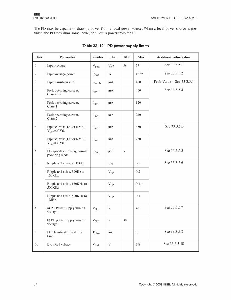
IEEE Std 802.3af-2003 AMENDMENT TO IEEE Std 802.3
The PD may be capable of drawing power from a local power source. When a local power source is pro-vided, the PD may draw some, none, or all of its power from the PI.
Table 33–12—PD power supply limits
Item Parameter Symbol Unit Min Max Additional information
1 Input voltage VPort Vdc 36 57 See 33.3.5.1
2 Input average power PPort W 12.95 See 33.3.5.2
3 Input inrush current IInrush mA 400 Peak Value—See 33.3.5.3
4 Peak operating current,Class 0, 3
IPort mA 400 See 33.3.5.4
Peak operating current,Class 1
IPort mA 120
Peak operating current,Class 2
IPort mA 210
5 Input current (DC or RMS), VPort=37Vdc
IPort mA 350 See 33.3.5.3
Input current (DC or RMS), VPort=57Vdc
IPort mA 230
6 PI capacitance during normal powering mode
CPort µF 5 See 33.3.5.5
7 Ripple and noise, < 500Hz VPP 0.5 See 33.3.5.6
Ripple and noise, 500Hz to 150KHz
VPP 0.2
Ripple and noise, 150KHz to 500KHz
VPP 0.15
Ripple and noise, 500KHz to 1MHz
VPP 0.1
8 a) PD Power supply turn on voltage
VOn V 42 See 33.3.5.7
b) PD power supply turn off voltage
VOff V 30
9 PD classification stability time
Tclass ms 5 See 33.3.5.8
10 Backfeed voltage Vbfd V 2.8 See 33.3.5.10
54 Copyright © 2003 IEEE. All rights reserved.
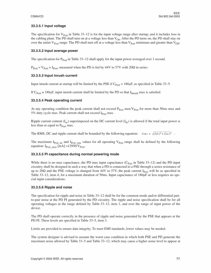
IEEE CSMA/CD Std 802.3af-2003
33.3.5.1 Input voltage
The specification for VPort in Table 33–12 is for the input voltage range after startup, and it includes loss inthe cabling plant. The PD shall turn on at a voltage less than VOn. After the PD turns on, the PD shall stay onover the entire VPort range. The PD shall turn off at a voltage less than VPort minimum and greater than VOff.
33.3.5.2 Input average power
The specification for PPort in Table 33–12 shall apply for the input power averaged over 1 second.
PPort = VPort × IPort, measured when the PD is fed by 44V to 57V with 20Ω in series.
33.3.5.3 Input inrush current
Input inrush current at startup will be limited by the PSE if CPort < 180µF, as specified in Table 33–5.
If CPort ≥ 180µF, input inrush current shall be limited by the PD so that IInrush max is satisfied.
33.3.5.4 Peak operating current
At any operating condition the peak current shall not exceed PPort max/VPort for more than 50ms max and5% duty cycle max. Peak current shall not exceed IPort max.
Ripple current content (Iac) superimposed on the DC current level (Idc) is allowed if the total input power isless than or equal to PPort max.
The RMS, DC and ripple current shall be bounded by the following equation: .
The maximum IPort_dc and IPort_rms values for all operating VPort range shall be defined by the followingequation: IPort_max [mA] =12950/VPort.
33.3.5.5 PI capacitance during normal powering mode
While there is no max capacitance, the PD max input capacitance (CPort in Table 33–12) and the PD inputcircuitry shall be designed in such a way that when a PD is connected to a PSE through a series resistance ofup to 20Ω and the PSE voltage is changed from 44V to 57V, the peak current IPort will be as specified inTable 33–12, item 4, for a maximum duration of 50ms. Input capacitance of 180µF or less requires no spe-cial input considerations.
33.3.5.6 Ripple and noise
The specification for ripple and noise in Table 33–12 shall be for the common-mode and/or differential pair-to-pair noise at the PD PI generated by the PD circuitry. The ripple and noise specification shall be for alloperating voltages in the range defined by Table 33–12, item 1, and over the range of input power of thedevice.
The PD shall operate correctly in the presence of ripple and noise generated by the PSE that appears at thePD PI. These levels are specified in Table 33–5, item 3.
Limits are provided to ensure data integrity. To meet EMI standards, lower values may be needed.
The system designer is advised to assume the worst case condition in which both PSE and PD generate themaximum noise allowed by Table 33–5 and Table 33–12, which may cause a higher noise level to appear at
Irms Idc( )2 Iac( )2+=
Copyright © 2003 IEEE. All rights reserved. 55

IEEE Std 802.3af-2003 AMENDMENT TO IEEE Std 802.3
the PI than the standalone case as specified by this clause.
33.3.5.7 PD power supply turn on / turn off voltages
The PD shall turn on at VOn and turn off at VOff (as specified in Table 33–12) when connected to a PSEthrough a 20Ω series resistor. The PD shall turn on or off without startup oscillation and within the first trialat any load value.
33.3.5.8 PD classification stability time
The PD classification signature shall be valid within Tclass as specified in Table 33–12 and remain valid forthe duration of the classification period.
33.3.5.9 PD stability
NOTE—Caution, when connected together as a system, the PSE and PD might exhibit instability at the PSE side or thePD side or both due to the presence of negative impedance at the PD input. See Annex 33D for PD design guidelines toensure stable operation.
33.3.5.10 Backfeed Voltage
When VPort max is applied across the PI at either polarity specified on the conductors for Mode A accordingto Table 33–7, the voltage measured across the PI for Mode B with a 100KΩ load resistor connected shallnot exceed Vbfd max as specified in Table 33–12. When VPort max is applied across the PI at either polarityspecified on the conductors for Mode B according to Table 33–7, the voltage measured across the PI forMode A with a 100KΩ load resistor connected shall not exceed Vbfd max.
33.3.6 PD Maintain Power Signature
In order to maintain power, the PD shall provide a valid Maintain Power Signature (MPS) at the PI. TheMPS shall be both:
a) Current draw equal or above the minimum Input current (IPort min) as specified in Table 33–13 for aminimum duration of 75ms followed by an optional MPS dropout for no longer than 250ms, and
b) Input impedance with resistive and capacitive components as defined in Table 33–13.
A PD that does not maintain any one of:
c) The minimum input current as defined in Table 33–13 for at least 75ms, and
d) Input impedance with resistive and capacitive components as defined by Table 33–13 (also, see Fig-ure 33–10 and Figure 33–11),
may have its power removed within the limits of TMPDO as specified in Table 33–5.
Powered PDs that no longer require power shall remove both components a) and b) of the MPS. To ensurepower removal, the impedance of the PI must rise above Zac2 as specified in Table 33–6.
56 Copyright © 2003 IEEE. All rights reserved.
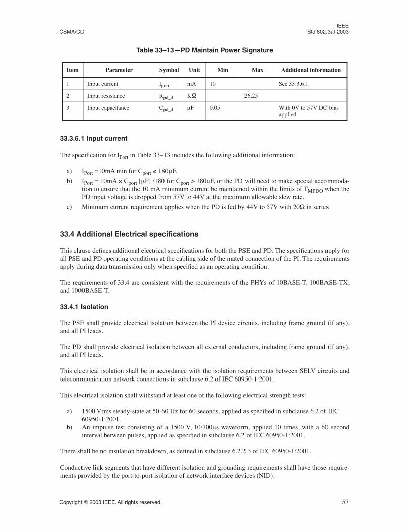
IEEE
CSMA/CD Std 802.3af-2003
33.3.6.1 Input current
The specification for IPort in Table 33–13 includes the following additional information:
a) IPort =10mA min for Cport ≤ 180µF.
b) IPort = 10mA × Cport [µF] /180 for Cport > 180µF, or the PD will need to make special accommoda-tion to ensure that the 10 mA minimum current be maintained within the limits of TMPDO when thePD input voltage is dropped from 57V to 44V at the maximum allowable slew rate.
c) Minimum current requirement applies when the PD is fed by 44V to 57V with 20Ω in series.
33.4 Additional Electrical specifications
This clause defines additional electrical specifications for both the PSE and PD. The specifications apply forall PSE and PD operating conditions at the cabling side of the mated connection of the PI. The requirementsapply during data transmission only when specified as an operating condition.
The requirements of 33.4 are consistent with the requirements of the PHYs of 10BASE-T, 100BASE-TX,and 1000BASE-T.
33.4.1 Isolation
The PSE shall provide electrical isolation between the PI device circuits, including frame ground (if any),and all PI leads.
The PD shall provide electrical isolation between all external conductors, including frame ground (if any),and all PI leads.
This electrical isolation shall be in accordance with the isolation requirements between SELV circuits andtelecommunication network connections in subclause 6.2 of IEC 60950-1:2001.
This electrical isolation shall withstand at least one of the following electrical strength tests:
a) 1500 Vrms steady-state at 50-60 Hz for 60 seconds, applied as specified in subclause 6.2 of IEC60950-1:2001.
b) An impulse test consisting of a 1500 V, 10/700µs waveform, applied 10 times, with a 60 secondinterval between pulses, applied as specified in subclause 6.2 of IEC 60950-1:2001.
There shall be no insulation breakdown, as defined in subclause 6.2.2.3 of IEC 60950-1:2001.
Conductive link segments that have different isolation and grounding requirements shall have those require-ments provided by the port-to-port isolation of network interface devices (NID).
Table 33–13—PD Maintain Power Signature
Item Parameter Symbol Unit Min Max Additional information
1 Input current Iport mA 10 See 33.3.6.1
2 Input resistance Rpd_d KΩ 26.25
3 Input capacitance Cpd_d µF 0.05 With 0V to 57V DC bias applied
Copyright © 2003 IEEE. All rights reserved. 57
IEEE Std 802.3af-2003 AMENDMENT TO IEEE Std 802.3
33.4.1.1 Electrical isolation environments
There are two electrical power distribution environments to be considered that require different electricalisolation properties. They are as follows:
— Environment A: When a LAN or LAN segment, with all its associated interconnected equipment, isentirely contained within a single low-voltage power distribution system and within a singlebuilding.
— Environment B: When a LAN crosses the boundary between separate power distribution systems orthe boundaries of a single building.
33.4.1.1.1 Environment A requirements
Attachment of network segments via NIDs that have multiple instances of a twisted pair MDI requires elec-trical isolation between each segment and the protective ground of the NID.
For NIDs, the requirement for isolation is encompassed within the isolation requirements of the basic MAU/PHY/medium standard. (See 14.3.1.1, TP-PMD, and 40.6.1.1.) Equipment with multiple instances of PSEand/or PD shall meet or exceed the isolation requirement of the MAU/PHY with which they are associated.
A multi-port NID complying with Environment A requirements does not require electrical power isolationbetween link segments.
An Environment A PSE shall switch the more negative conductor. It is allowable to switch both conductors.
33.4.1.1.2 Environment B requirements
The attachment of network segments that cross environment A boundaries requires electrical isolationbetween each segment and all other attached segments as well as to the protective ground of the NID.
For NIDs, the requirement for isolation is encompassed within the isolation requirements of the basic MAU/PHY/medium standard (See 14.3.1.1, TP-PMD, and 40.6.1.1.). Equipment with multiple instances of PSEand/or PD shall meet or exceed the isolation requirement of the MAU/PHY with which each is associated.
The requirements for interconnected electrically conducting link segments that are partially or fully externalto a single building environment may require additional protection against lightning strikes or other hazards.Protection requirements for such hazards are beyond the scope of this standard. Guidance on these require-ments may be found in Section 6 of IEC 60950-1:2001, as well as any local and national codes related tosafety.
33.4.2 Fault tolerance
Each wire pair of the PSE or PD when it is encompassed within the MDI shall meet the fault tolerancerequirements of the appropriate specifying clause, (See 14.3.1.2.7, Clause 25, and 40.8.3.4). When a PSE isnot encompassed within an MDI, the PSE PI shall meet the fault tolerance requirements of this subclause.
The PSE PI shall withstand without damage the application of short circuits of any wire to any other wirewithin the cable for an indefinite period of time. The magnitude of the current through such a short circuitshall not exceed ILIM max as defined in Table 33–5, item 10.
Each wire pair shall withstand, without damage, a 1000V common-mode impulse applied at Ecm of eitherpolarity (as indicated in Figure 33–13). The shape of the impulse shall be (0.3/50)µs (300ns virtual front
58 Copyright © 2003 IEEE. All rights reserved.
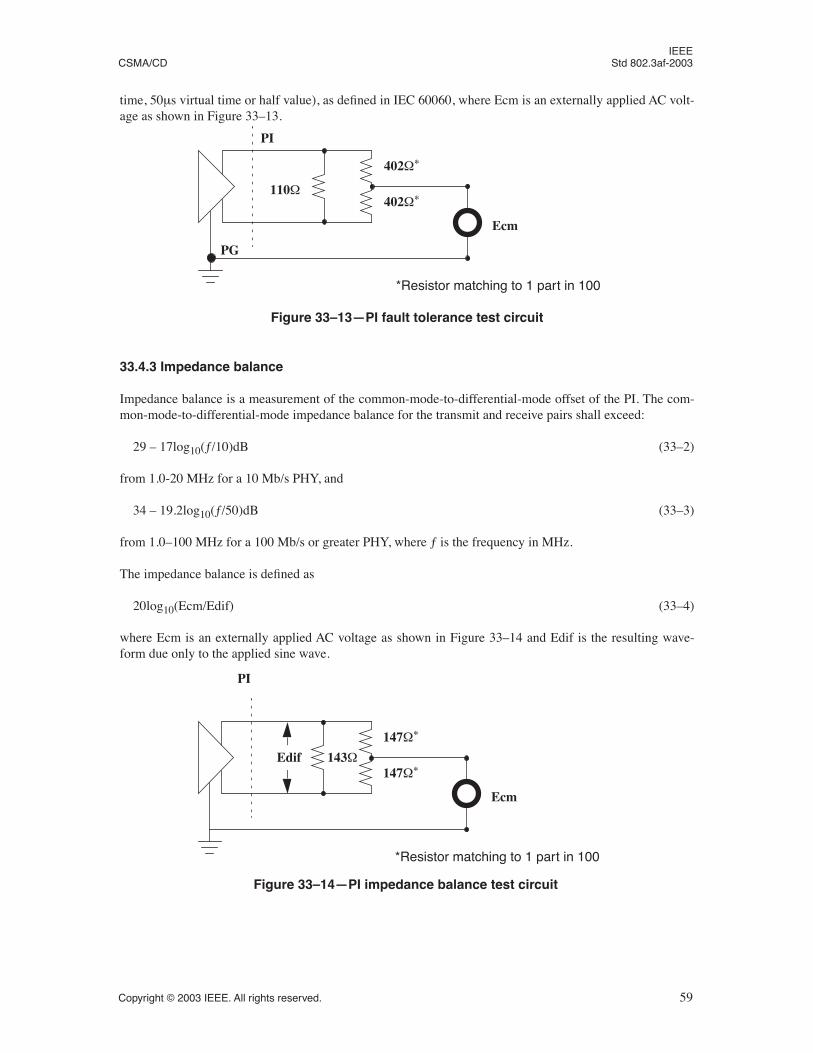
IEEE
CSMA/CD Std 802.3af-2003
time, 50µs virtual time or half value), as defined in IEC 60060, where Ecm is an externally applied AC volt-age as shown in Figure 33–13.
33.4.3 Impedance balance
Impedance balance is a measurement of the common-mode-to-differential-mode offset of the PI. The com-mon-mode-to-differential-mode impedance balance for the transmit and receive pairs shall exceed:
29 – 17log10(ƒ/10)dB (33–2)
from 1.0-20 MHz for a 10 Mb/s PHY, and
34 – 19.2log10(ƒ/50)dB (33–3)
from 1.0–100 MHz for a 100 Mb/s or greater PHY, where ƒ is the frequency in MHz.
The impedance balance is defined as
20log10(Ecm/Edif) (33–4)
where Ecm is an externally applied AC voltage as shown in Figure 33–14 and Edif is the resulting wave-form due only to the applied sine wave.
402Ω∗
402Ω∗110Ω
*Resistor matching to 1 part in 100
Ecm
Figure 33–13—PI fault tolerance test circuit
PI
PG
147Ω∗
147Ω∗143Ω
*Resistor matching to 1 part in 100
Ecm
PI
Edif
Figure 33–14—PI impedance balance test circuit
Copyright © 2003 IEEE. All rights reserved. 59
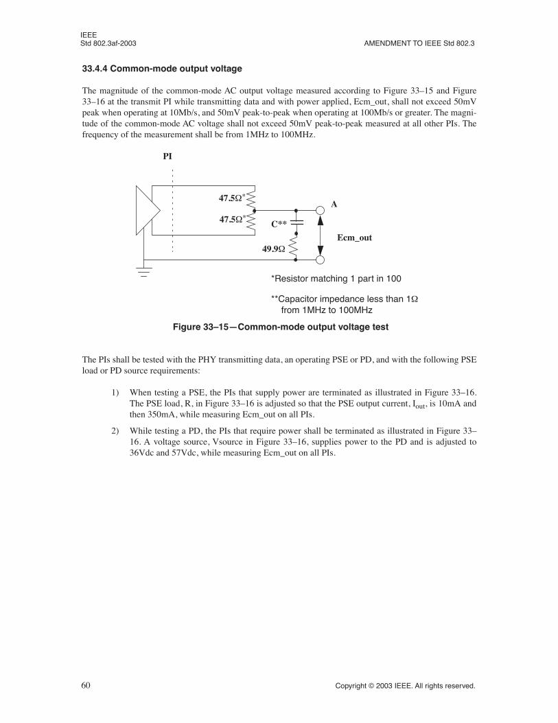
IEEE Std 802.3af-2003 AMENDMENT TO IEEE Std 802.3
33.4.4 Common-mode output voltage
The magnitude of the common-mode AC output voltage measured according to Figure 33–15 and Figure33–16 at the transmit PI while transmitting data and with power applied, Ecm_out, shall not exceed 50mVpeak when operating at 10Mb/s, and 50mV peak-to-peak when operating at 100Mb/s or greater. The magni-tude of the common-mode AC voltage shall not exceed 50mV peak-to-peak measured at all other PIs. Thefrequency of the measurement shall be from 1MHz to 100MHz.
The PIs shall be tested with the PHY transmitting data, an operating PSE or PD, and with the following PSEload or PD source requirements:
1) When testing a PSE, the PIs that supply power are terminated as illustrated in Figure 33–16.The PSE load, R, in Figure 33–16 is adjusted so that the PSE output current, Iout, is 10mA andthen 350mA, while measuring Ecm_out on all PIs.
2) While testing a PD, the PIs that require power shall be terminated as illustrated in Figure 33–16. A voltage source, Vsource in Figure 33–16, supplies power to the PD and is adjusted to36Vdc and 57Vdc, while measuring Ecm_out on all PIs.
47.5Ω∗
47.5Ω∗
49.9Ω
*Resistor matching 1 part in 100
Ecm_out
PI
A
Figure 33–15—Common-mode output voltage test
C**
**Capacitor impedance less than 1Ωfrom 1MHz to 100MHz
60 Copyright © 2003 IEEE. All rights reserved.
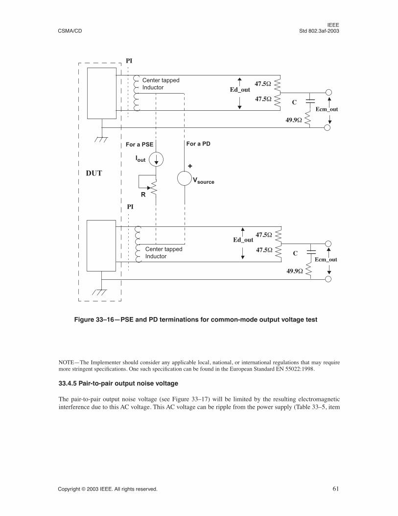
IEEE CSMA/CD Std 802.3af-2003
NOTE—The Implementer should consider any applicable local, national, or international regulations that may requiremore stringent specifications. One such specification can be found in the European Standard EN 55022:1998.
33.4.5 Pair-to-pair output noise voltage
The pair-to-pair output noise voltage (see Figure 33–17) will be limited by the resulting electromagneticinterference due to this AC voltage. This AC voltage can be ripple from the power supply (Table 33–5, item
Figure 33–16—PSE and PD terminations for common-mode output voltage test
PI
47.5Ω
47.5Ω
49.9Ω
Ecm_outC
47.5Ω
47.5Ω
49.9Ω
C
Ed_out
Ed_out
R
Iout
For a PSE
Ecm_out
For a PD
Vsource
+
Center tappedInductor
Center tappedInductor
DUT
PI
Copyright © 2003 IEEE. All rights reserved. 61
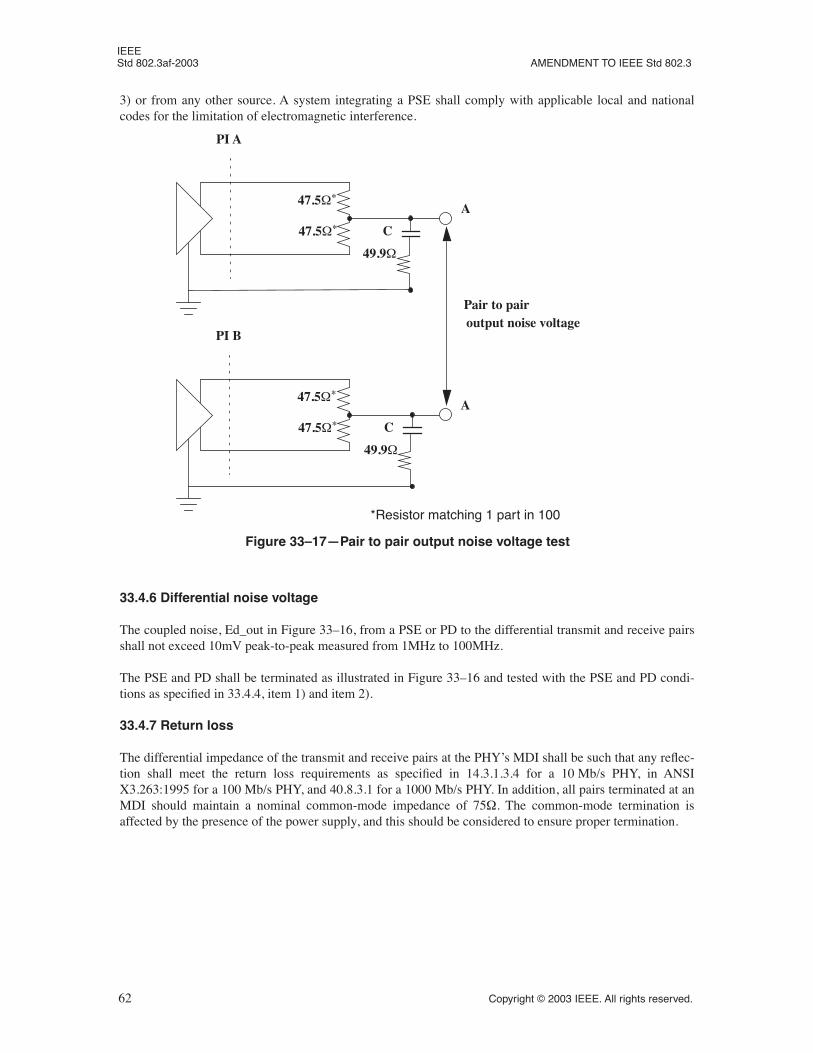
IEEE Std 802.3af-2003 AMENDMENT TO IEEE Std 802.3
3) or from any other source. A system integrating a PSE shall comply with applicable local and nationalcodes for the limitation of electromagnetic interference.
33.4.6 Differential noise voltage
The coupled noise, Ed_out in Figure 33–16, from a PSE or PD to the differential transmit and receive pairsshall not exceed 10mV peak-to-peak measured from 1MHz to 100MHz.
The PSE and PD shall be terminated as illustrated in Figure 33–16 and tested with the PSE and PD condi-tions as specified in 33.4.4, item 1) and item 2).
33.4.7 Return loss
The differential impedance of the transmit and receive pairs at the PHY’s MDI shall be such that any reflec-tion shall meet the return loss requirements as specified in 14.3.1.3.4 for a 10 Mb/s PHY, in ANSIX3.263:1995 for a 100 Mb/s PHY, and 40.8.3.1 for a 1000 Mb/s PHY. In addition, all pairs terminated at anMDI should maintain a nominal common-mode impedance of 75Ω. The common-mode termination isaffected by the presence of the power supply, and this should be considered to ensure proper termination.
47.5Ω∗
47.5Ω∗
*Resistor matching 1 part in 100
Pair to pair
PI B
A
Figure 33–17—Pair to pair output noise voltage test
47.5Ω∗
47.5Ω∗
49.9Ω
PI A
A
output noise voltage
C
49.9Ω
C
62 Copyright © 2003 IEEE. All rights reserved.
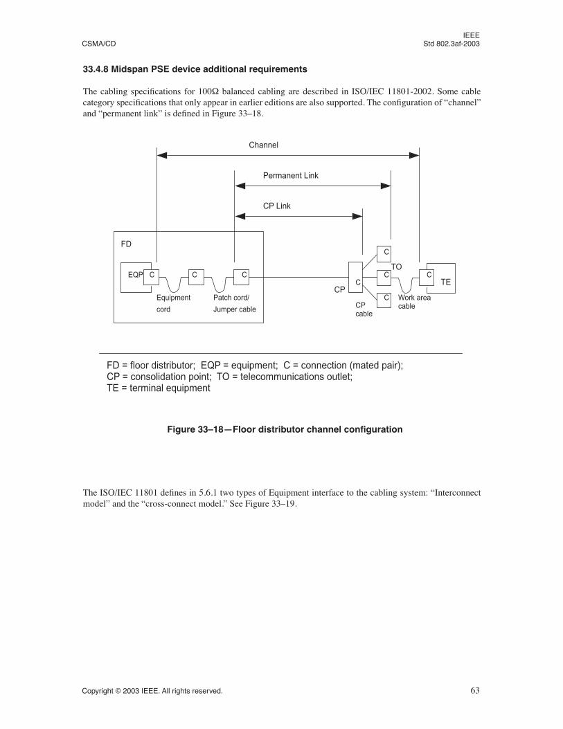
IEEE CSMA/CD Std 802.3af-2003
33.4.8 Midspan PSE device additional requirements
The cabling specifications for 100Ω balanced cabling are described in ISO/IEC 11801-2002. Some cablecategory specifications that only appear in earlier editions are also supported. The configuration of “channel”and “permanent link” is defined in Figure 33–18.
The ISO/IEC 11801 defines in 5.6.1 two types of Equipment interface to the cabling system: “Interconnectmodel” and the “cross-connect model.” See Figure 33–19.
Equipment
cord
Patch cord/
Jumper cable CPcable
Work areacable
FD
EQP
CPTE
C C CC
C
C
C
C
Channel
Permanent Link
CP Link
FD = floor distributor; EQP = equipment; C = connection (mated pair);CP = consolidation point; TO = telecommunications outlet;TE = terminal equipment
TO
Figure 33–18—Floor distributor channel configuration
Copyright © 2003 IEEE. All rights reserved. 63
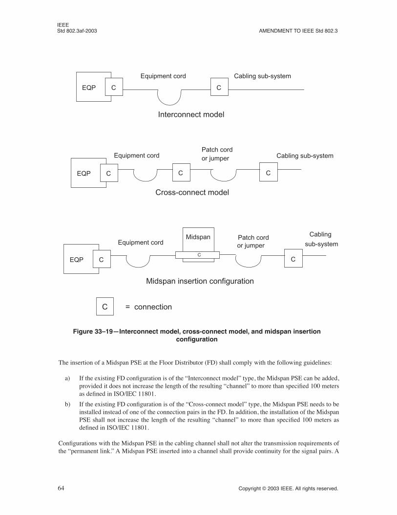
IEEE Std 802.3af-2003 AMENDMENT TO IEEE Std 802.3
The insertion of a Midspan PSE at the Floor Distributor (FD) shall comply with the following guidelines:
a) If the existing FD configuration is of the “Interconnect model” type, the Midspan PSE can be added,provided it does not increase the length of the resulting “channel” to more than specified 100 metersas defined in ISO/IEC 11801.
b) If the existing FD configuration is of the “Cross-connect model” type, the Midspan PSE needs to beinstalled instead of one of the connection pairs in the FD. In addition, the installation of the MidspanPSE shall not increase the length of the resulting “channel” to more than specified 100 meters asdefined in ISO/IEC 11801.
Configurations with the Midspan PSE in the cabling channel shall not alter the transmission requirements ofthe “permanent link.” A Midspan PSE inserted into a channel shall provide continuity for the signal pairs. A
Equipment cord Cabling sub-system
Equipment cord Cabling sub-systemPatch cordor jumper
C C
C C C
EQP
EQP
Interconnect model
Cross-connect model
C = connection
Figure 33–19—Interconnect model, cross-connect model, and midspan insertion configuration
CEQP
Patch cordor jumper
CC
MidspanEquipment cord
Cabling
sub-system
Midspan insertion configuration
64 Copyright © 2003 IEEE. All rights reserved.
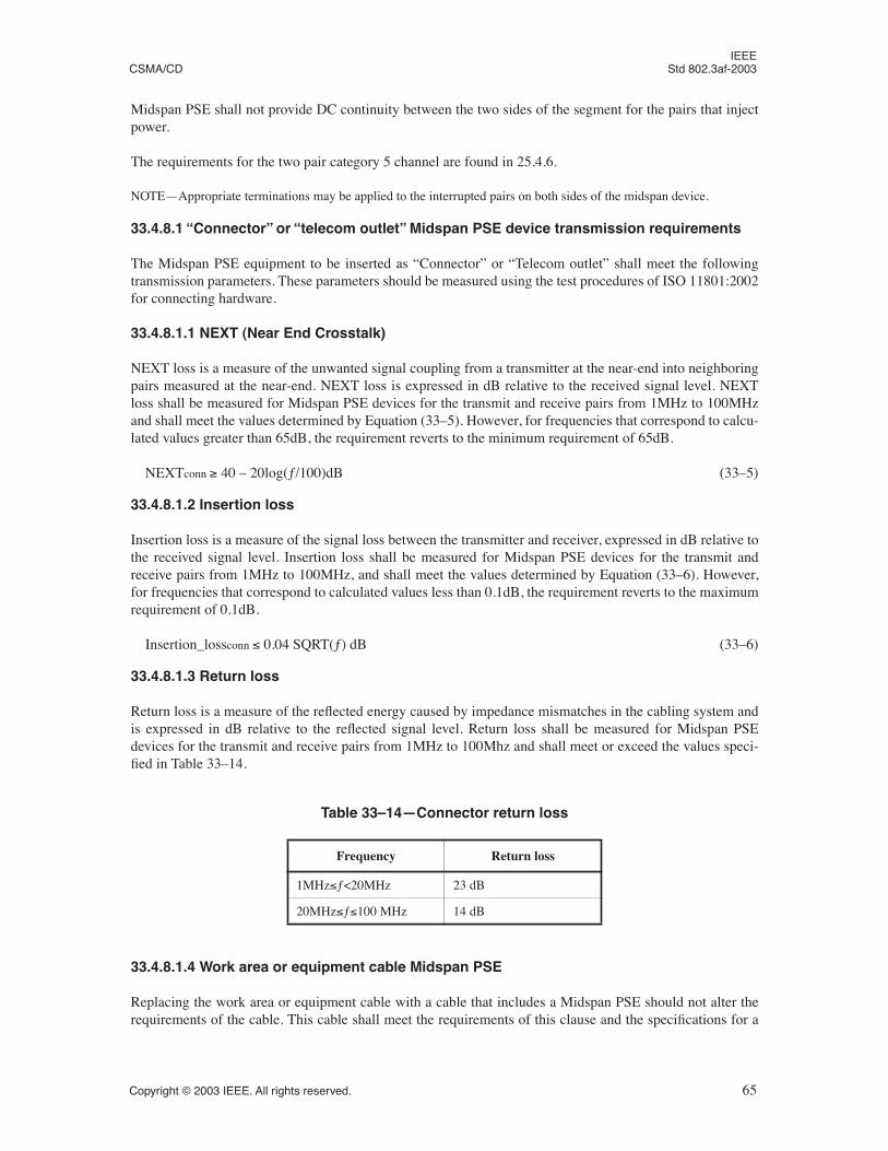
IEEE
CSMA/CD Std 802.3af-2003
Midspan PSE shall not provide DC continuity between the two sides of the segment for the pairs that injectpower.
The requirements for the two pair category 5 channel are found in 25.4.6.
NOTE—Appropriate terminations may be applied to the interrupted pairs on both sides of the midspan device.
33.4.8.1 “Connector” or “telecom outlet” Midspan PSE device transmission requirements
The Midspan PSE equipment to be inserted as “Connector” or “Telecom outlet” shall meet the followingtransmission parameters. These parameters should be measured using the test procedures of ISO 11801:2002for connecting hardware.
33.4.8.1.1 NEXT (Near End Crosstalk)
NEXT loss is a measure of the unwanted signal coupling from a transmitter at the near-end into neighboringpairs measured at the near-end. NEXT loss is expressed in dB relative to the received signal level. NEXTloss shall be measured for Midspan PSE devices for the transmit and receive pairs from 1MHz to 100MHzand shall meet the values determined by Equation (33–5). However, for frequencies that correspond to calcu-lated values greater than 65dB, the requirement reverts to the minimum requirement of 65dB.
NEXTconn ≥ 40 – 20log(ƒ/100)dB (33–5)
33.4.8.1.2 Insertion loss
Insertion loss is a measure of the signal loss between the transmitter and receiver, expressed in dB relative tothe received signal level. Insertion loss shall be measured for Midspan PSE devices for the transmit andreceive pairs from 1MHz to 100MHz, and shall meet the values determined by Equation (33–6). However,for frequencies that correspond to calculated values less than 0.1dB, the requirement reverts to the maximumrequirement of 0.1dB.
Insertion_lossconn ≤ 0.04 SQRT(ƒ) dB (33–6)
33.4.8.1.3 Return loss
Return loss is a measure of the reflected energy caused by impedance mismatches in the cabling system andis expressed in dB relative to the reflected signal level. Return loss shall be measured for Midspan PSEdevices for the transmit and receive pairs from 1MHz to 100Mhz and shall meet or exceed the values speci-fied in Table 33–14.
33.4.8.1.4 Work area or equipment cable Midspan PSE
Replacing the work area or equipment cable with a cable that includes a Midspan PSE should not alter therequirements of the cable. This cable shall meet the requirements of this clause and the specifications for a
Table 33–14—Connector return loss
Frequency Return loss
1MHz≤ƒ<20MHz 23 dB
20MHz≤ƒ≤100 MHz 14 dB
Copyright © 2003 IEEE. All rights reserved. 65
IEEE Std 802.3af-2003 AMENDMENT TO IEEE Std 802.3
Category 5 (jumper) cord as specified in ISO/IEC 11801:2002 for insertion loss, NEXT, and return loss forthe transmit and receive pairs.
33.5 Environmental
33.5.1 General safety
All equipment meeting this standard shall conform to IEC 60950-1:2001. In particular, the PSE shall beclassified as a Limited Power Source in accordance with IEC 60950-1:2001.
Equipment shall comply with all applicable local and national codes related to safety.
33.5.2 Network safety
This subclause sets forth a number of recommendations and guidelines related to safety concerns. The list isneither complete nor does it address all possible safety issues. The designer is urged to consult the relevantlocal, national, and international safety regulations to ensure compliance with the appropriate requirements.LAN cabling systems described in this clause are subject to at least four direct electrical safety hazards dur-ing their installation and use. These hazards are as follows:
a) Direct contact between LAN components and power, lighting, or communications circuits.b) Static charge buildup on LAN cabling and components.c) High-energy transients coupled onto the LAN cabling system.d) Voltage potential differences between safety grounds to which various LAN components are
connected.
Such electrical safety hazards must be avoided or appropriately protected against for proper network instal-lation and performance. In addition to provisions for proper handling of these conditions in an operationalsystem, special measures must be taken to ensure that the intended safety features are not negated duringinstallation of a new network or during modification of an existing network.
33.5.3 Installation and maintenance guidelines
It is a mandatory requirement that sound installation practice, as defined by applicable local codes and regu-lations, be followed in every instance in which such practice is applicable.
It is a mandatory requirement that, during installation of the cabling plant, care be taken to ensure that non-insulated network cabling conductors do not make electrical contact with unintended conductors or ground.
33.5.4 Patch panel considerations
It is possible that the current carrying capability of a cabling cross-connect may be exceeded by a PSE. Thedesigner should consult the manufacturers’ specifications to ensure compliance with the appropriaterequirements.
33.5.5 Cabling resistance unbalance
Resistance unbalance is a measure of the difference in resistance between the two conductors in the 100Ωbalanced cabling system. The resistance unbalance shall be as specified in IEC 11801 Edition 2, Clause 6.4.8(reference: 3 percent).
The resistance unbalance as defined in IEC 61156-1 is
66 Copyright © 2003 IEEE. All rights reserved.
IEEE CSMA/CD Std 802.3af-2003
((Rmax – Rmin)/(Rmax + Rmin)) × 100 percent, (33–7)
where Rmax is the resistance of the conductor with the highest resistance, and Rmin is the resistance of theconductor with the lowest resistance.
33.5.6 Telephony voltages
The use of building wiring brings with it the possibility of wiring errors that may connect telephony voltagesto a PSE or PD. Other than voice signals, the primary voltages that may be encountered are the “battery” andringing voltages. Although there is no universal standard, the following maximums generally apply:
Battery voltage to a telephone line is generally 56Vdc, applied to the line through a balanced 400Ω sourceimpedance. Ringing voltage is a composite signal consisting of an AC component and a DC component. TheAC component is up to 175Vp at 20Hz to 60Hz with a 100Ω source resistance. The DC component is 56Vdcwith 300Ω to 600Ω source resistance. Large reactive transients can occur at the start and end of each ringinterval.
Application of any of the above voltages to the PI of a PSE or a PD shall not result in any safety hazard.
33.5.7 Electromagnetic emissions
The PD and PSE powered cabling link shall comply with applicable local and national codes for the limita-tion of electromagnetic interference.
33.5.8 Temperature and humidity
The PD and PSE powered cabling link segment is expected to operate over a reasonable range of environ-mental conditions related to temperature, humidity, and physical handling. Specific requirements and valuesfor these parameters are beyond the scope of this standard.
33.5.9 Labeling
It is recommended that the PSE or PD (and supporting documentation) be labeled in a manner visible to theuser with at least the following parameters:
a) Power classification and power level in terms of maximum current drain over the operating voltagerange, 44V to 57V, applies for PD only,
b) Port type (e.g., 100BASE-TX, TIA Category or ISO Class),c) Any applicable safety warnings, andd) “PSE” or “PD” as appropriate.
33.6 Management function requirements
Management of the PSE is optional. If the PSE is instantiated in the same physical package as a PHY and aClause 22 MII or a Clause 35 GMII is physically implemented, then management access shall be via the MIIManagement interface. Where no physical embodiment of the MII or GMII exists and management is sup-ported, equivalent management capability shall be provided.
33.6.1 PSE registers
A PSE shall use register address 11 for its control and register address 12 for its status functions.
Copyright © 2003 IEEE. All rights reserved. 67
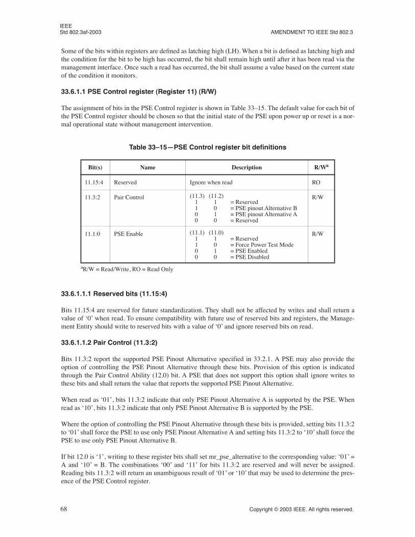
IEEE Std 802.3af-2003 AMENDMENT TO IEEE Std 802.3
Some of the bits within registers are defined as latching high (LH). When a bit is defined as latching high andthe condition for the bit to be high has occurred, the bit shall remain high until after it has been read via themanagement interface. Once such a read has occurred, the bit shall assume a value based on the current stateof the condition it monitors.
33.6.1.1 PSE Control register (Register 11) (R/W)
The assignment of bits in the PSE Control register is shown in Table 33–15. The default value for each bit ofthe PSE Control register should be chosen so that the initial state of the PSE upon power up or reset is a nor-mal operational state without management intervention.
33.6.1.1.1 Reserved bits (11.15:4)
Bits 11.15:4 are reserved for future standardization. They shall not be affected by writes and shall return avalue of ‘0’ when read. To ensure compatibility with future use of reserved bits and registers, the Manage-ment Entity should write to reserved bits with a value of ‘0’ and ignore reserved bits on read.
33.6.1.1.2 Pair Control (11.3:2)
Bits 11.3:2 report the supported PSE Pinout Alternative specified in 33.2.1. A PSE may also provide theoption of controlling the PSE Pinout Alternative through these bits. Provision of this option is indicatedthrough the Pair Control Ability (12.0) bit. A PSE that does not support this option shall ignore writes tothese bits and shall return the value that reports the supported PSE Pinout Alternative.
When read as ‘01’, bits 11.3:2 indicate that only PSE Pinout Alternative A is supported by the PSE. Whenread as ‘10’, bits 11.3:2 indicate that only PSE Pinout Alternative B is supported by the PSE.
Where the option of controlling the PSE Pinout Alternative through these bits is provided, setting bits 11.3:2to ‘01’ shall force the PSE to use only PSE Pinout Alternative A and setting bits 11.3:2 to ‘10’ shall force thePSE to use only PSE Pinout Alternative B.
If bit 12.0 is ‘1’, writing to these register bits shall set mr_pse_alternative to the corresponding value: ‘01’ =A and ‘10’ = B. The combinations ‘00’ and ‘11’ for bits 11.3:2 are reserved and will never be assigned.Reading bits 11.3:2 will return an unambiguous result of ‘01’ or ‘10’ that may be used to determine the pres-ence of the PSE Control register.
Table 33–15—PSE Control register bit definitions
Bit(s) Name Description R/Wa
aR/W = Read/Write, RO = Read Only
11.15:4 Reserved Ignore when read RO
11.3:2 Pair Control (11.3) (11.2)1 1 = Reserved1 0 = PSE pinout Alternative B0 1 = PSE pinout Alternative A0 0 = Reserved
R/W
11.1:0 PSE Enable (11.1) (11.0)1 1 = Reserved1 0 = Force Power Test Mode0 1 = PSE Enabled0 0 = PSE Disabled
R/W
68 Copyright © 2003 IEEE. All rights reserved.
IEEE CSMA/CD Std 802.3af-2003
33.6.1.1.3 PSE Enable (11.1:0)
The PSE function shall be disabled by setting bits 11.1 to logic zero and 11.0 to logic zero. When the PSEfunction is disabled, the MDI shall function as it would if it had no PSE function. The PSE function shall beenabled by setting bits 11.1 to a logic zero and 11.0 to a logic one. When bit 11.1 is a logic one, and bit 11.0is a logic zero, a test mode is enabled. This test mode supplies power without regard to PD detection.
Writing to these register bits shall set mr_pse_enable to the corresponding value: ‘00’ = disable, ‘01’ =enable and ‘10’ = force power. The combination ‘11’ for bits 11.1:0 has been reserved for future use.
NOTE—Caution, test mode may damage connected non-PD, legacy, twisted pair Ethernet devices or other non-Ethernetdevices, especially in split application wiring schemes.
33.6.1.2 PSE Status register (Register 12) (R/W)
The assignment of bits in the PSE Status register is shown in Table 33–16.
33.6.1.2.1 Reserved bits (12.15:13)
Bits 12.15:13 are reserved for future standardization. They shall not be affected by writes and shall return avalue of ‘0’ when read. To ensure compatibility with future use of reserved bits and registers, the Manage-ment Entity should write to reserved bits with a value of ‘0’ and ignore reserved bits on read.
33.6.1.2.2 Power Denied (12.12)
When read as a logic one, bit 12.12 indicates that power has been denied. This bit shall be set to ‘1’ when thePSE state diagram (Figure 33–6) enters the state ‘POWER_DENIED’. The Power Denied bit shall be imple-mented with latching high behavior as defined in 33.6.1.
33.6.1.2.3 Valid Signature (12.11)
When read as a logic one, bit 12.11 indicates that a valid signature has been detected. This bit shall be set to‘1’ when mr_valid_signature transitions from FALSE to TRUE. The Valid Signature bit shall be imple-mented with latching high behavior as defined in 33.6.1.
33.6.1.2.4 Invalid Signature (12.10)
When read as a logic one, bit 12.10 indicates that an invalid signature has been detected. This bit shall be setto ‘1’ when the PSE state diagram (Figure 33–6) enters the state ‘SIGNATURE_INVALID’. The Invalid Sig-nature bit shall be implemented with latching high behavior as defined in 33.6.1.
33.6.1.2.5 Short Circuit (12.9)
When read as a logic one, bit 12.9 indicates that a short circuit condition has been detected. This bit shall beset to ‘1’ when the PSE state diagram (Figure 33–6) enters the state ‘ERROR_DELAY_SHORT’. The ShortCircuit bit shall be implemented with latching high behavior as defined in 33.6.1.
33.6.1.2.6 Overload (12.8)
When read as a logic one, bit 12.8 indicates that an overload condition has been detected. This bit shall be setto ‘1’ when the PSE state diagram (Figure 33–6) enters the state ‘ERROR_DELAY_OVER’. The Overloadbit shall be implemented with latching high behavior as defined in 33.6.1.
Copyright © 2003 IEEE. All rights reserved. 69
IEEE Std 802.3af-2003 AMENDMENT TO IEEE Std 802.3
33.6.1.2.7 MPS Absent (12.7)
When read as a logic one, bit 12.7 indicates that an MPS Absent condition has been detected. The MPSAbsent bit shall be set to ‘1’ when the PSE state diagram (Figure 33–6) transitions directly from the statePOWER_ON to IDLE due to tpmdo_timer_done being asserted. The MPS Absent bit shall be implementedwith latching high behavior as defined in 33.6.1.
Table 33–16—PSE Status register bit definitions
Bit(s) Name Description R/Wa
12.15:13 Reserved Ignore when read RO
12.12 Power Denied 1 = Power has been denied0 = Power has not been denied
RO/LH
12.11 Valid Signature 1 = Valid PD signature detected0 = No valid PD signature detected
RO/LH
12.10 Invalid Signature 1 = Invalid PD signature detected0 = No invalid PD signature detected
RO/LH
12.9 Short Circuit 1 = Short circuit condition detected0 = No short circuit condition detected
RO/LH
12.8 Overload 1 = Overload condition detected0 = No overload condition detected
RO/LH
12.7 MPS Absent 1 = MPS absent condition detected0 = No MPS absent condition detected
RO/LH
12.6:4 PD Class (12.6) (12.5) (12.4)1 1 1 = Reserved1 1 0 = Reserved1 0 1 = Reserved1 0 0 = Class 40 1 1 = Class 30 1 0 = Class 20 0 1 = Class 10 0 0 = Class 0
RO
12.3:1 PSE Status (12.3) (12.2) (12.1)1 1 1 = Reserved1 1 0 = Reserved1 0 1 = Implementation specific fault1 0 0 = Test error0 1 1 = Test mode0 1 0 = Delivering power0 0 1 = Searching0 0 0 = Disabled
RO
12.0 Pair Control Ability 1 = PSE pinout controllable by Pair Control bits0 = PSE pinout Alternative fixed
RO
aRO = Read Only, LH = Latched High
70 Copyright © 2003 IEEE. All rights reserved.
IEEE CSMA/CD Std 802.3af-2003
33.6.1.2.8 PD Class (12.6:4)
Bits 12.6:4 report the PD Class of a detected PD as specified in 33.2.6 and 33.2.7. The value in this registeris valid while a PD is connected, i.e., while the PSE Status (12.3:1) bits are reporting Delivering Power. Thecombinations ‘101’, ‘110’ and ‘111’ for bits 12.6:4 have been reserved for future use.
33.6.1.2.9 PSE Status (12.3:1)
Bits 12.3:1 report the current status of the PSE. When read as ‘000’, bits 12.3:1 indicate that the PSE statediagram (Figure 33–6) is in the state DISABLED. When read as ‘010’, bits 12.3:1 indicate that the PSE statediagram is in the state POWER_ON. When read as ‘011’, bits 12.3:1 indicate that the PSE state diagram is inthe state TEST_MODE. When read as ‘100’, bits 12.3:1 indicate that the PSE state diagram is in the stateTEST_ERROR. When read as ‘101’, bits 12.3:1 indicate that the PSE state diagram is in the state IDLE dueto the variable error_condition = true. When read as ‘001’, bits 12.3:1 indicate that the PSE state diagram isin a state other than those listed above.
The combinations ‘111’ and ‘110’ for bits 12.3:1 have been reserved for future use.
33.6.1.2.10 Pair Control Ability (12.0)
When read as a logic one, bit 12.0 indicates that the PSE supports the option to control which PSE PinoutAlternative (see 33.2.1) is used for PD detection and power through the Pair Control (11.3:2) bits. Whenread as a logic zero, bit 12.0 indicates that the PSE lacks support of the option to control which PSE PinoutAlternative is used for PD detection and power through the Pair Control (11.3:2) bits.
33.7 Protocol Implementation Conformance Statement (PICS) proforma for Clause 33, DTE Power via MDI
33.7.1 Introduction
The supplier of a protocol implementation that is claimed to conform to IEEE Std 802.3af-2003, DTE Power via MDI, shall complete the following Protocol Implementation Conformance Statement (PICS) proforma.
A detailed description of the symbols used in the PICS proforma, along with instructions for completing the PICS proforma, can be found in Clause 21.
Copyright © 2003 IEEE. All rights reserved. 71
IEEE Std 802.3af-2003 AMENDMENT TO IEEE Std 802.3
33.7.2 Identification
33.7.2.1 Implementation identification
33.7.2.2 Protocol summary
33.7.2.3 PD Major capabilities/options
Supplier1
Contact point for enquiries about the PICS1
Implementation Name(s) and Version(s)1,3
Other information necessary for full identification—e.g., name(s) and version(s) for machines and/or operating systems; System Name(s)2
1—Required for all implementations
2—May be completed as appropriate in meeting the requirements for the identification.
3—The terms Name and Version should be interpreted appropriately to correspond with a supplier’s terminology(e.g., Type, Series, Model).
Identification of protocol standard IEEE Std 802.3af-2003, Clause 33, DTE Power via MDI
Identification of amendments and corrigenda to this PICS proforma that have been completed as part of this PICS
Have any Exception items been required? No [ ] Yes [ ](See Clause 21; the answer Yes means that the implementation does not conform to the standard.)
Date of Statement
Item Feature Subclause Value/Comment Status Support
*PDCL PD Classification 33.3.4 PD supports classification O Yes [ ]No [ ]
72 Copyright © 2003 IEEE. All rights reserved.
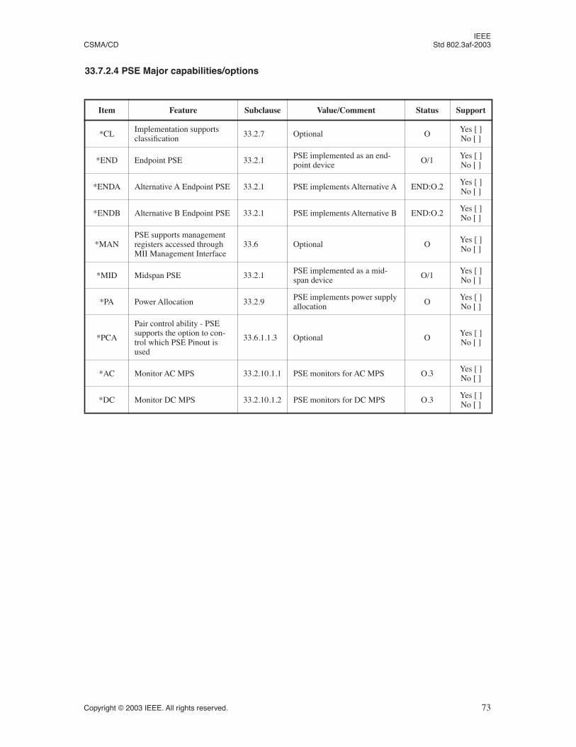
IEEE CSMA/CD Std 802.3af-2003
33.7.2.4 PSE Major capabilities/options
Item Feature Subclause Value/Comment Status Support
*CL Implementation supports classification 33.2.7 Optional O Yes [ ]
No [ ]
*END Endpoint PSE 33.2.1 PSE implemented as an end-point device O/1 Yes [ ]
No [ ]
*ENDA Alternative A Endpoint PSE 33.2.1 PSE implements Alternative A END:O.2 Yes [ ]No [ ]
*ENDB Alternative B Endpoint PSE 33.2.1 PSE implements Alternative B END:O.2 Yes [ ]No [ ]
*MANPSE supports management registers accessed through MII Management Interface
33.6 Optional O Yes [ ]No [ ]
*MID Midspan PSE 33.2.1 PSE implemented as a mid-span device O/1 Yes [ ]
No [ ]
*PA Power Allocation 33.2.9 PSE implements power supply allocation O Yes [ ]
No [ ]
*PCA
Pair control ability - PSE supports the option to con-trol which PSE Pinout is used
33.6.1.1.3 Optional O Yes [ ]No [ ]
*AC Monitor AC MPS 33.2.10.1.1 PSE monitors for AC MPS O.3 Yes [ ]No [ ]
*DC Monitor DC MPS 33.2.10.1.2 PSE monitors for DC MPS O.3 Yes [ ]No [ ]
Copyright © 2003 IEEE. All rights reserved. 73
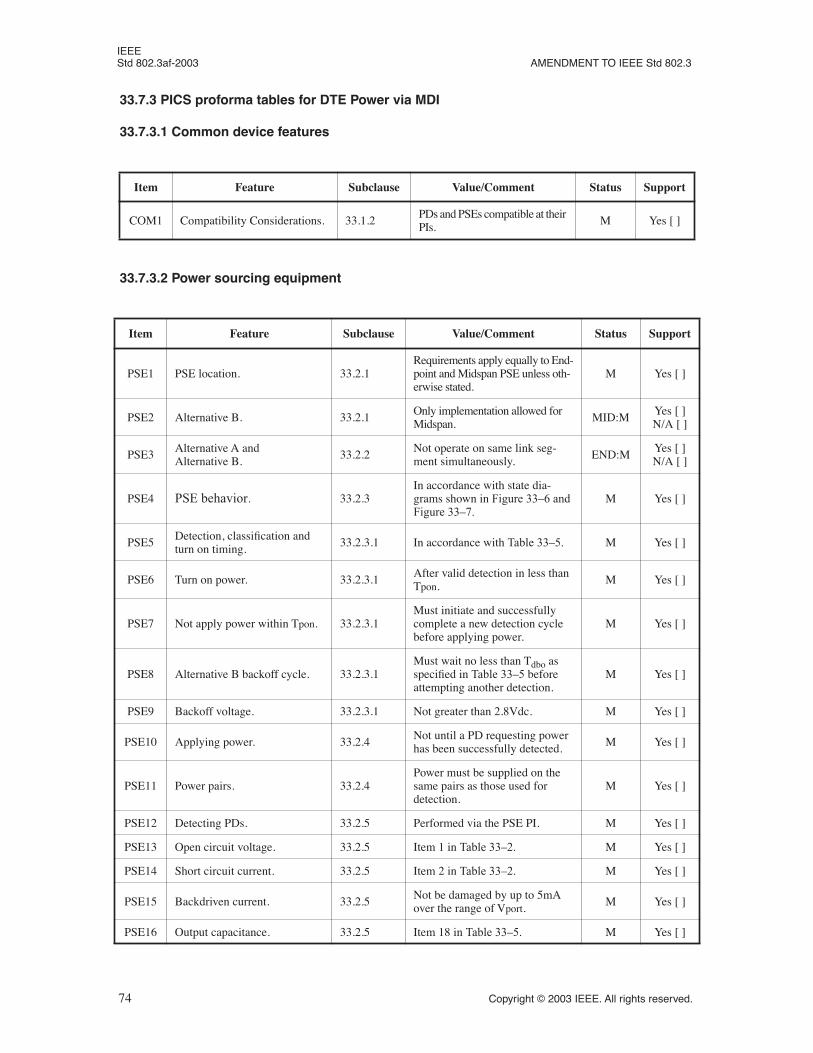
IEEE Std 802.3af-2003 AMENDMENT TO IEEE Std 802.3
33.7.3 PICS proforma tables for DTE Power via MDI
33.7.3.1 Common device features
33.7.3.2 Power sourcing equipment
Item Feature Subclause Value/Comment Status Support
COM1 Compatibility Considerations. 33.1.2 PDs and PSEs compatible at their PIs. M Yes [ ]
Item Feature Subclause Value/Comment Status Support
PSE1 PSE location. 33.2.1Requirements apply equally to End-point and Midspan PSE unless oth-erwise stated.
M Yes [ ]
PSE2 Alternative B. 33.2.1 Only implementation allowed for Midspan. MID:M Yes [ ]
N/A [ ]
PSE3 Alternative A and Alternative B. 33.2.2 Not operate on same link seg-
ment simultaneously. END:M Yes [ ]N/A [ ]
PSE4 PSE behavior. 33.2.3In accordance with state dia-grams shown in Figure 33–6 and
Figure 33–7.
M Yes [ ]
PSE5 Detection, classification and turn on timing. 33.2.3.1 In accordance with Table 33–5. M Yes [ ]
PSE6 Turn on power. 33.2.3.1 After valid detection in less than Tpon. M Yes [ ]
PSE7 Not apply power within Tpon. 33.2.3.1Must initiate and successfully complete a new detection cycle before applying power.
M Yes [ ]
PSE8 Alternative B backoff cycle. 33.2.3.1Must wait no less than Tdbo as specified in Table 33–5 before attempting another detection.
M Yes [ ]
PSE9 Backoff voltage. 33.2.3.1 Not greater than 2.8Vdc. M Yes [ ]
PSE10 Applying power. 33.2.4 Not until a PD requesting power has been successfully detected. M Yes [ ]
PSE11 Power pairs. 33.2.4Power must be supplied on the same pairs as those used for detection.
M Yes [ ]
PSE12 Detecting PDs. 33.2.5 Performed via the PSE PI. M Yes [ ]
PSE13 Open circuit voltage. 33.2.5 Item 1 in Table 33–2. M Yes [ ]
PSE14 Short circuit current. 33.2.5 Item 2 in Table 33–2. M Yes [ ]
PSE15 Backdriven current. 33.2.5 Not be damaged by up to 5mA over the range of Vport. M Yes [ ]
PSE16 Output capacitance. 33.2.5 Item 18 in Table 33–5. M Yes [ ]
74 Copyright © 2003 IEEE. All rights reserved.
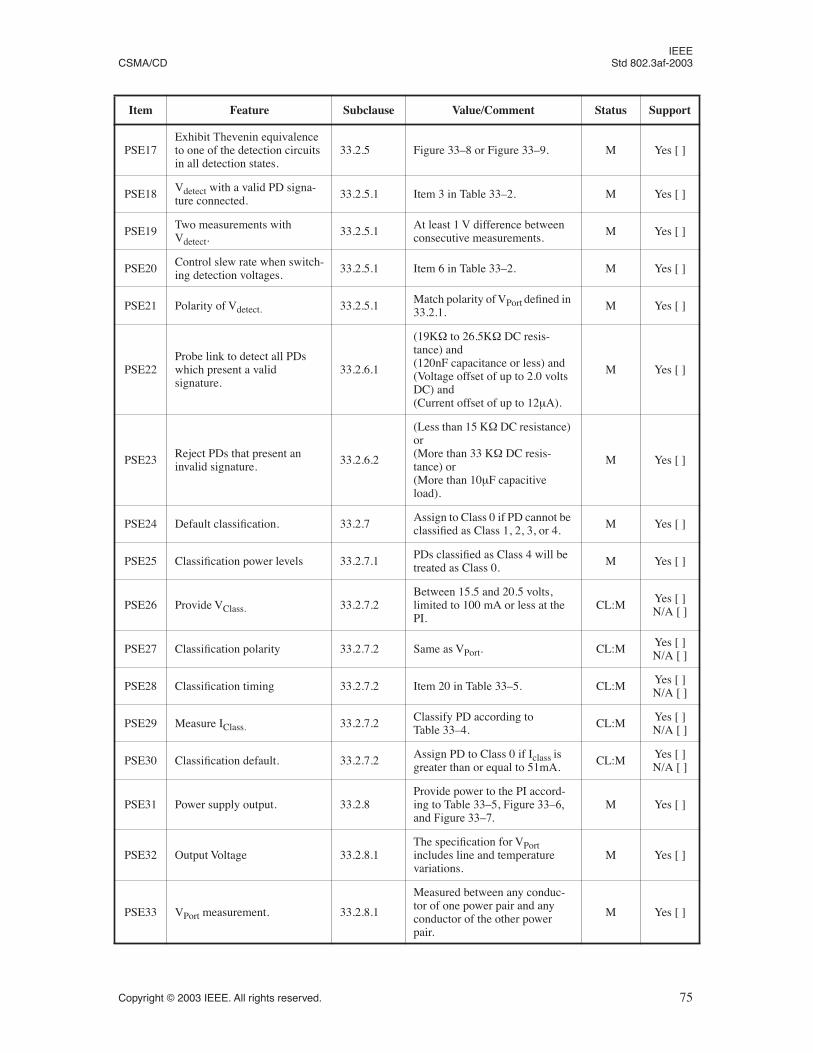
IEEE CSMA/CD Std 802.3af-2003
PSE17Exhibit Thevenin equivalence
to one of the detection circuits in all detection states.
33.2.5 Figure 33–8 or Figure 33–9. M Yes [ ]
PSE18 Vdetect with a valid PD signa-ture connected. 33.2.5.1 Item 3 in Table 33–2. M Yes [ ]
PSE19 Two measurements with Vdetect.
33.2.5.1 At least 1 V difference between consecutive measurements. M Yes [ ]
PSE20 Control slew rate when switch-ing detection voltages. 33.2.5.1 Item 6 in Table 33–2. M Yes [ ]
PSE21 Polarity of Vdetect. 33.2.5.1 Match polarity of VPort defined in 33.2.1. M Yes [ ]
PSE22Probe link to detect all PDs which present a valid signature.
33.2.6.1
(19KΩ to 26.5KΩ DC resis-tance) and(120nF capacitance or less) and(Voltage offset of up to 2.0 volts DC) and(Current offset of up to 12µA).
M Yes [ ]
PSE23 Reject PDs that present an invalid signature. 33.2.6.2
(Less than 15 KΩ DC resistance) or(More than 33 KΩ DC resis-tance) or(More than 10µF capacitive load).
M Yes [ ]
PSE24 Default classification. 33.2.7 Assign to Class 0 if PD cannot be classified as Class 1, 2, 3, or 4. M Yes [ ]
PSE25 Classification power levels 33.2.7.1 PDs classified as Class 4 will be treated as Class 0. M Yes [ ]
PSE26 Provide VClass. 33.2.7.2Between 15.5 and 20.5 volts, limited to 100 mA or less at the PI.
CL:M Yes [ ]N/A [ ]
PSE27 Classification polarity 33.2.7.2 Same as VPort. CL:M Yes [ ]N/A [ ]
PSE28 Classification timing 33.2.7.2 Item 20 in Table 33–5. CL:M Yes [ ]N/A [ ]
PSE29 Measure IClass. 33.2.7.2 Classify PD according to Table 33–4. CL:M Yes [ ]
N/A [ ]
PSE30 Classification default. 33.2.7.2 Assign PD to Class 0 if Iclass is greater than or equal to 51mA. CL:M Yes [ ]
N/A [ ]
PSE31 Power supply output. 33.2.8Provide power to the PI accord-ing to Table 33–5, Figure 33–6,
and Figure 33–7.
M Yes [ ]
PSE32 Output Voltage 33.2.8.1The specification for VPort includes line and temperature variations.
M Yes [ ]
PSE33 VPort measurement. 33.2.8.1
Measured between any conduc-tor of one power pair and any conductor of the other power pair.
M Yes [ ]
Item Feature Subclause Value/Comment Status Support
Copyright © 2003 IEEE. All rights reserved. 75
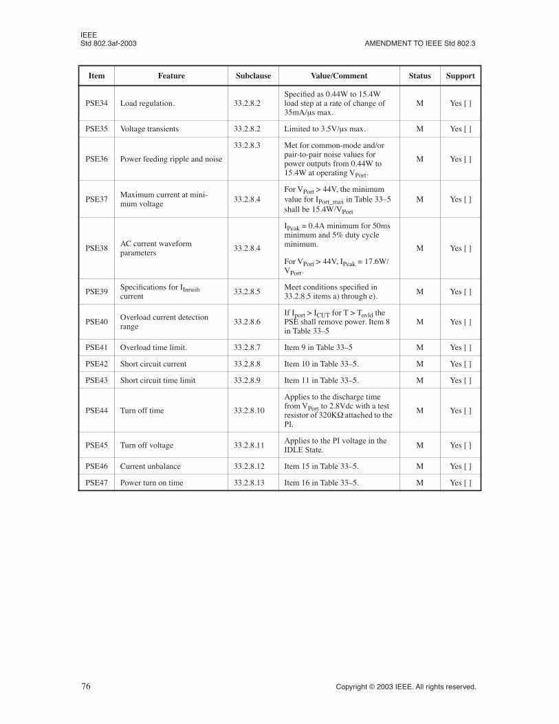
IEEE Std 802.3af-2003 AMENDMENT TO IEEE Std 802.3
PSE34 Load regulation. 33.2.8.2Specified as 0.44W to 15.4W load step at a rate of change of 35mA/µs max.
M Yes [ ]
PSE35 Voltage transients 33.2.8.2 Limited to 3.5V/µs max. M Yes [ ]
PSE36 Power feeding ripple and noise
33.2.8.3 Met for common-mode and/or pair-to-pair noise values for power outputs from 0.44W to 15.4W at operating VPort.
M Yes [ ]
PSE37 Maximum current at mini-mum voltage 33.2.8.4
For VPort > 44V, the minimum value for IPort_max in Table 33–5 shall be 15.4W/VPort
M Yes [ ]
PSE38 AC current waveform parameters 33.2.8.4
IPeak = 0.4A minimum for 50ms minimum and 5% duty cycle minimum.
For VPort > 44V, IPeak = 17.6W/VPort.
M Yes [ ]
PSE39 Specifications for IInrush current 33.2.8.5 Meet conditions specified in
33.2.8.5 items a) through e). M Yes [ ]
PSE40 Overload current detection range 33.2.8.6
If Iport > ICUT for T > Tovld the PSE shall remove power. Item 8 in Table 33–5
M Yes [ ]
PSE41 Overload time limit. 33.2.8.7 Item 9 in Table 33–5 M Yes [ ]
PSE42 Short circuit current 33.2.8.8 Item 10 in Table 33–5. M Yes [ ]
PSE43 Short circuit time limit 33.2.8.9 Item 11 in Table 33–5. M Yes [ ]
PSE44 Turn off time 33.2.8.10
Applies to the discharge time from VPort to 2.8Vdc with a test resistor of 320KΩ attached to the
PI.
M Yes [ ]
PSE45 Turn off voltage 33.2.8.11 Applies to the PI voltage in the
IDLE State.M Yes [ ]
PSE46 Current unbalance 33.2.8.12 Item 15 in Table 33–5. M Yes [ ]
PSE47 Power turn on time 33.2.8.13 Item 16 in Table 33–5. M Yes [ ]
Item Feature Subclause Value/Comment Status Support
76 Copyright © 2003 IEEE. All rights reserved.
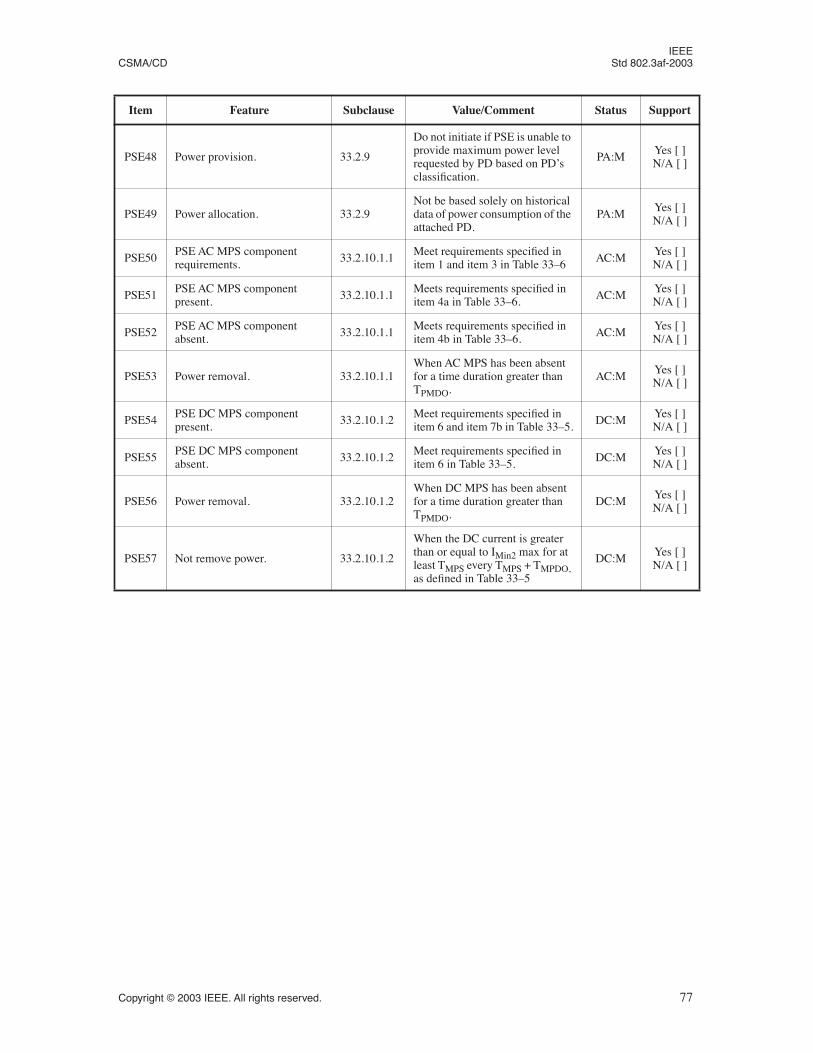
IEEE CSMA/CD Std 802.3af-2003
PSE48 Power provision. 33.2.9
Do not initiate if PSE is unable to provide maximum power level requested by PD based on PD’s classification.
PA:M Yes [ ]N/A [ ]
PSE49 Power allocation. 33.2.9Not be based solely on historical data of power consumption of the attached PD.
PA:M Yes [ ]N/A [ ]
PSE50 PSE AC MPS component requirements. 33.2.10.1.1 Meet requirements specified in
item 1 and item 3 in Table 33–6 AC:M Yes [ ]N/A [ ]
PSE51 PSE AC MPS component present. 33.2.10.1.1 Meets requirements specified in
item 4a in Table 33–6. AC:M Yes [ ]N/A [ ]
PSE52 PSE AC MPS component absent. 33.2.10.1.1 Meets requirements specified in
item 4b in Table 33–6. AC:M Yes [ ]N/A [ ]
PSE53 Power removal. 33.2.10.1.1When AC MPS has been absent for a time duration greater than TPMDO.
AC:M Yes [ ]N/A [ ]
PSE54 PSE DC MPS component present. 33.2.10.1.2 Meet requirements specified in
item 6 and item 7b in Table 33–5. DC:M Yes [ ]N/A [ ]
PSE55 PSE DC MPS component absent. 33.2.10.1.2 Meet requirements specified in
item 6 in Table 33–5. DC:M Yes [ ]N/A [ ]
PSE56 Power removal. 33.2.10.1.2When DC MPS has been absent for a time duration greater than TPMDO.
DC:M Yes [ ]N/A [ ]
PSE57 Not remove power. 33.2.10.1.2
When the DC current is greater than or equal to IMin2 max for at least TMPS every TMPS + TMPDO, as defined in Table 33–5
DC:M Yes [ ]N/A [ ]
Item Feature Subclause Value/Comment Status Support
Copyright © 2003 IEEE. All rights reserved. 77
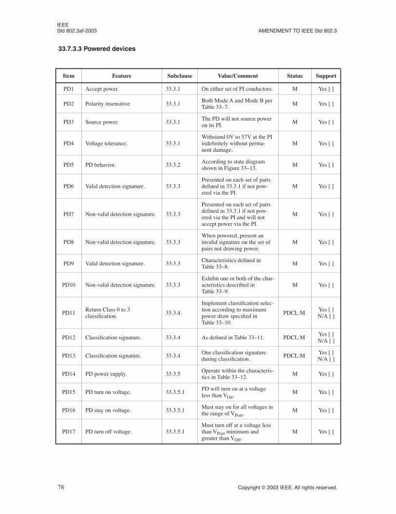
IEEE Std 802.3af-2003 AMENDMENT TO IEEE Std 802.3
33.7.3.3 Powered devices
Item Feature Subclause Value/Comment Status Support
PD1 Accept power. 33.3.1 On either set of PI conductors. M Yes [ ]
PD2 Polarity insensitive 33.3.1 Both Mode A and Mode B per Table 33–7. M Yes [ ]
PD3 Source power. 33.3.1 The PD will not source power on its PI. M Yes [ ]
PD4 Voltage tolerance. 33.3.1Withstand 0V to 57V at the PI indefinitely without perma-nent damage.
M Yes [ ]
PD5 PD behavior. 33.3.2 According to state diagram shown in Figure 33–13. M Yes [ ]
PD6 Valid detection signature. 33.3.3Presented on each set of pairs defined in 33.3.1 if not pow-ered via the PI.
M Yes [ ]
PD7 Non-valid detection signature. 33.3.3
Presented on each set of pairs defined in 33.3.1 if not pow-ered via the PI and will not accept power via the PI.
M Yes [ ]
PD8 Non-valid detection signature. 33.3.3When powered, present an invalid signature on the set of pairs not drawing power.
M Yes [ ]
PD9 Valid detection signature. 33.3.3 Characteristics defined in Table 33–8. M Yes [ ]
PD10 Non-valid detection signature. 33.3.3Exhibit one or both of the char-acteristics described in Table 33–9.
M Yes [ ]
PD11 Return Class 0 to 3 classification. 33.3.4
Implement classification selec-tion according to maximum power draw specified in Table 33–10.
PDCL:M Yes [ ]N/A [ ]
PD12 Classification signature. 33.3.4 As defined in Table 33–11. PDCL:M Yes [ ]N/A [ ]
PD13 Classification signature. 33.3.4 One classification signature during classification. PDCL:M Yes [ ]
N/A [ ]
PD14 PD power supply. 33.3.5 Operate within the characteris-tics in Table 33–12. M Yes [ ]
PD15 PD turn on voltage. 33.3.5.1 PD will turn on at a voltage less than VOn. M Yes [ ]
PD16 PD stay on voltage. 33.3.5.1 Must stay on for all voltages in the range of VPort.
M Yes [ ]
PD17 PD turn off voltage. 33.3.5.1Must turn off at a voltage less than VPort minimum and greater than VOff.
M Yes [ ]
78 Copyright © 2003 IEEE. All rights reserved.
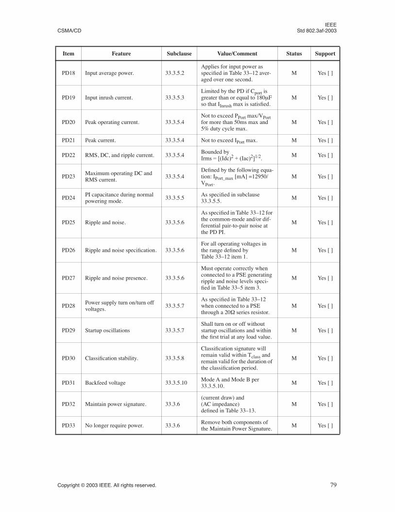
IEEE CSMA/CD Std 802.3af-2003
PD18 Input average power. 33.3.5.2Applies for input power as specified in Table 33–12 aver-aged over one second.
M Yes [ ]
PD19 Input inrush current. 33.3.5.3Limited by the PD if Cport is greater than or equal to 180µF so that IInrush max is satisfied.
M Yes [ ]
PD20 Peak operating current. 33.3.5.4Not to exceed PPort max/VPort for more than 50ms max and 5% duty cycle max.
M Yes [ ]
PD21 Peak current. 33.3.5.4 Not to exceed IPort max. M Yes [ ]
PD22 RMS, DC, and ripple current. 33.3.5.4 Bounded by Irms = [(Idc)2 + (Iac)2]1/2.
M Yes [ ]
PD23 Maximum operating DC and RMS current. 33.3.5.4
Defined by the following equa-tion: IPort_max [mA] =12950/VPort.
M Yes [ ]
PD24 PI capacitance during normal powering mode. 33.3.5.5 As specified in subclause
33.3.5.5. M Yes [ ]
PD25 Ripple and noise. 33.3.5.6
As specified in Table 33–12 for the common-mode and/or dif-ferential pair-to-pair noise at the PD PI.
M Yes [ ]
PD26 Ripple and noise specification. 33.3.5.6For all operating voltages in the range defined by Table 33–12 item 1.
M Yes [ ]
PD27 Ripple and noise presence. 33.3.5.6
Must operate correctly when connected to a PSE generating ripple and noise levels speci-fied in Table 33–5 item 3.
M Yes [ ]
PD28 Power supply turn on/turn off voltages. 33.3.5.7
As specified in Table 33–12 when connected to a PSE through a 20Ω series resistor.
M Yes [ ]
PD29 Startup oscillations 33.3.5.7Shall turn on or off without startup oscillations and within the first trial at any load value.
M Yes [ ]
PD30 Classification stability. 33.3.5.8
Classification signature will remain valid within Tclass and remain valid for the duration of the classification period.
M Yes [ ]
PD31 Backfeed voltage 33.3.5.10 Mode A and Mode B per 33.3.5.10. M Yes [ ]
PD32 Maintain power signature. 33.3.6(current draw) and(AC impedance) defined in Table 33–13.
M Yes [ ]
PD33 No longer require power. 33.3.6 Remove both components of the Maintain Power Signature. M Yes [ ]
Item Feature Subclause Value/Comment Status Support
Copyright © 2003 IEEE. All rights reserved. 79
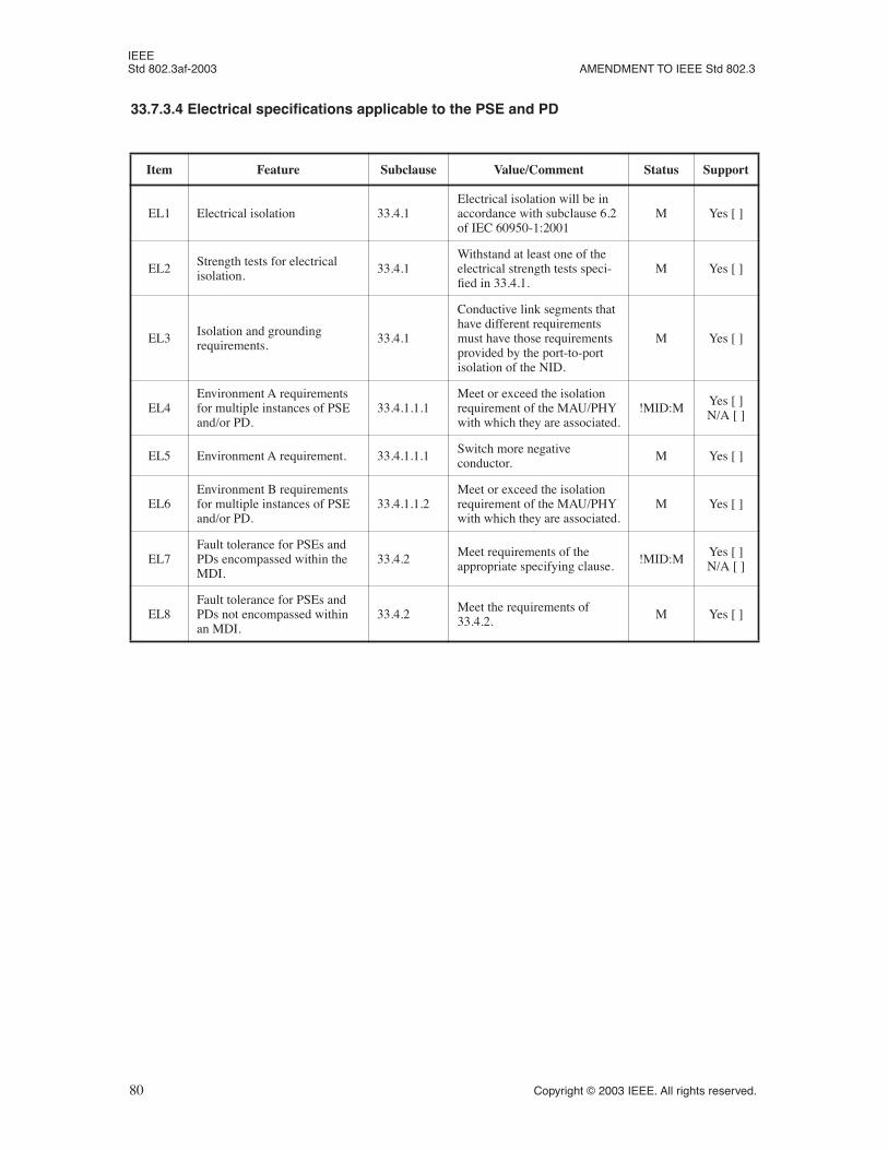
IEEE Std 802.3af-2003 AMENDMENT TO IEEE Std 802.3
33.7.3.4 Electrical specifications applicable to the PSE and PD
Item Feature Subclause Value/Comment Status Support
EL1 Electrical isolation 33.4.1Electrical isolation will be in accordance with subclause 6.2 of IEC 60950-1:2001
M Yes [ ]
EL2 Strength tests for electrical isolation. 33.4.1
Withstand at least one of the electrical strength tests speci-fied in 33.4.1.
M Yes [ ]
EL3 Isolation and grounding requirements. 33.4.1
Conductive link segments that have different requirements must have those requirements provided by the port-to-port isolation of the NID.
M Yes [ ]
EL4Environment A requirements for multiple instances of PSE and/or PD.
33.4.1.1.1Meet or exceed the isolation requirement of the MAU/PHY with which they are associated.
!MID:M Yes [ ]N/A [ ]
EL5 Environment A requirement. 33.4.1.1.1 Switch more negative conductor. M Yes [ ]
EL6Environment B requirements for multiple instances of PSE and/or PD.
33.4.1.1.2Meet or exceed the isolation requirement of the MAU/PHY with which they are associated.
M Yes [ ]
EL7Fault tolerance for PSEs and PDs encompassed within the MDI.
33.4.2 Meet requirements of the appropriate specifying clause. !MID:M Yes [ ]
N/A [ ]
EL8Fault tolerance for PSEs and PDs not encompassed within an MDI.
33.4.2 Meet the requirements of 33.4.2. M Yes [ ]
80 Copyright © 2003 IEEE. All rights reserved.
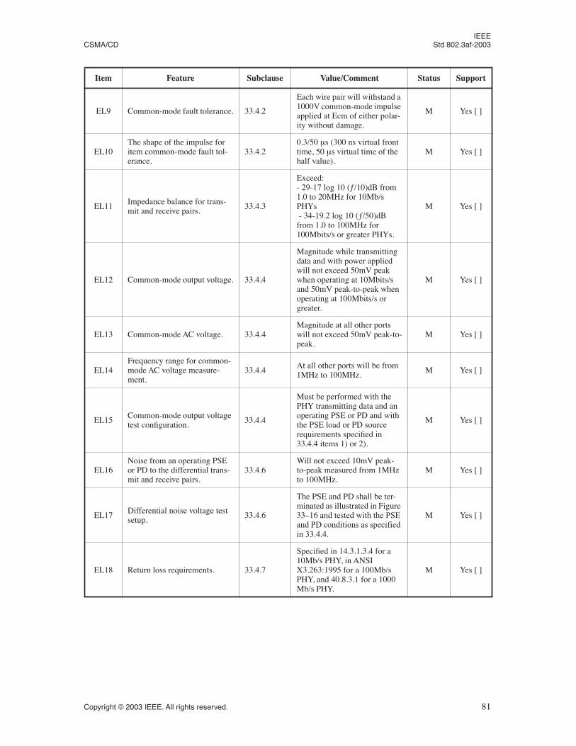
IEEE CSMA/CD Std 802.3af-2003
EL9 Common-mode fault tolerance. 33.4.2
Each wire pair will withstand a 1000V common-mode impulse applied at Ecm of either polar-ity without damage.
M Yes [ ]
EL10The shape of the impulse for item common-mode fault tol-erance.
33.4.20.3/50 µs (300 ns virtual front time, 50 µs virtual time of the half value).
M Yes [ ]
EL11 Impedance balance for trans-mit and receive pairs. 33.4.3
Exceed: - 29-17 log 10 (ƒ/10)dB from 1.0 to 20MHz for 10Mb/s PHYs - 34-19.2 log 10 (ƒ/50)dB from 1.0 to 100MHz for 100Mbits/s or greater PHYs.
M Yes [ ]
EL12 Common-mode output voltage. 33.4.4
Magnitude while transmitting data and with power applied will not exceed 50mV peak when operating at 10Mbits/s and 50mV peak-to-peak when operating at 100Mbits/s or greater.
M Yes [ ]
EL13 Common-mode AC voltage. 33.4.4Magnitude at all other ports will not exceed 50mV peak-to-peak.
M Yes [ ]
EL14Frequency range for common-mode AC voltage measure-ment.
33.4.4 At all other ports will be from 1MHz to 100MHz. M Yes [ ]
EL15 Common-mode output voltage test configuration. 33.4.4
Must be performed with the PHY transmitting data and an operating PSE or PD and with the PSE load or PD source requirements specified in 33.4.4 items 1) or 2).
M Yes [ ]
EL16Noise from an operating PSE or PD to the differential trans-mit and receive pairs.
33.4.6Will not exceed 10mV peak-to-peak measured from 1MHz to 100MHz.
M Yes [ ]
EL17 Differential noise voltage test setup. 33.4.6
The PSE and PD shall be ter-minated as illustrated in Figure 33–16 and tested with the PSE
and PD conditions as specified
in 33.4.4.
M Yes [ ]
EL18 Return loss requirements. 33.4.7
Specified in 14.3.1.3.4 for a 10Mb/s PHY, in ANSI X3.263:1995 for a 100Mb/s PHY, and 40.8.3.1 for a 1000 Mb/s PHY.
M Yes [ ]
Item Feature Subclause Value/Comment Status Support
Copyright © 2003 IEEE. All rights reserved. 81
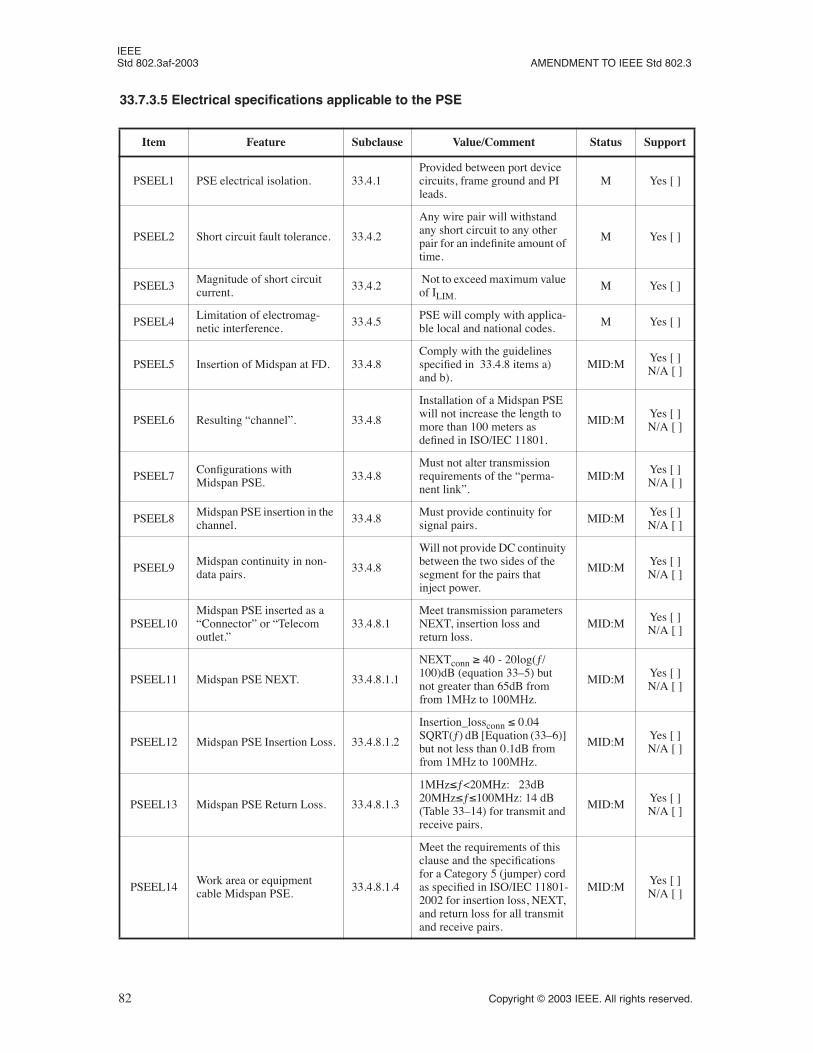
IEEE Std 802.3af-2003 AMENDMENT TO IEEE Std 802.3
33.7.3.5 Electrical specifications applicable to the PSE
Item Feature Subclause Value/Comment Status Support
PSEEL1 PSE electrical isolation. 33.4.1Provided between port device circuits, frame ground and PI leads.
M Yes [ ]
PSEEL2 Short circuit fault tolerance. 33.4.2
Any wire pair will withstand any short circuit to any other pair for an indefinite amount of time.
M Yes [ ]
PSEEL3 Magnitude of short circuit current. 33.4.2 Not to exceed maximum value
of ILIM.M Yes [ ]
PSEEL4 Limitation of electromag-netic interference. 33.4.5 PSE will comply with applica-
ble local and national codes. M Yes [ ]
PSEEL5 Insertion of Midspan at FD. 33.4.8Comply with the guidelines specified in 33.4.8 items a) and b).
MID:M Yes [ ]N/A [ ]
PSEEL6 Resulting “channel”. 33.4.8
Installation of a Midspan PSE will not increase the length to more than 100 meters as defined in ISO/IEC 11801.
MID:M Yes [ ]N/A [ ]
PSEEL7 Configurations with Midspan PSE. 33.4.8
Must not alter transmission requirements of the “perma-nent link”.
MID:M Yes [ ]N/A [ ]
PSEEL8 Midspan PSE insertion in the channel. 33.4.8 Must provide continuity for
signal pairs. MID:M Yes [ ]N/A [ ]
PSEEL9 Midspan continuity in non-data pairs. 33.4.8
Will not provide DC continuity between the two sides of the segment for the pairs that inject power.
MID:M Yes [ ]N/A [ ]
PSEEL10Midspan PSE inserted as a “Connector” or “Telecom outlet.”
33.4.8.1Meet transmission parameters NEXT, insertion loss and return loss.
MID:M Yes [ ]N/A [ ]
PSEEL11 Midspan PSE NEXT. 33.4.8.1.1
NEXTconn ≥ 40 - 20log(ƒ/100)dB (equation 33–5) but not greater than 65dB from from 1MHz to 100MHz.
MID:M Yes [ ]N/A [ ]
PSEEL12 Midspan PSE Insertion Loss. 33.4.8.1.2
Insertion_lossconn ≤ 0.04 SQRT(ƒ) dB [Equation (33–6)] but not less than 0.1dB from from 1MHz to 100MHz.
MID:M Yes [ ]N/A [ ]
PSEEL13 Midspan PSE Return Loss. 33.4.8.1.3
1MHz≤ƒ<20MHz: 23dB20MHz≤ƒ≤100MHz: 14 dB (Table 33–14) for transmit and receive pairs.
MID:M Yes [ ]N/A [ ]
PSEEL14 Work area or equipment cable Midspan PSE. 33.4.8.1.4
Meet the requirements of this clause and the specifications for a Category 5 (jumper) cord as specified in ISO/IEC 11801-2002 for insertion loss, NEXT, and return loss for all transmit and receive pairs.
MID:M Yes [ ]N/A [ ]
82 Copyright © 2003 IEEE. All rights reserved.
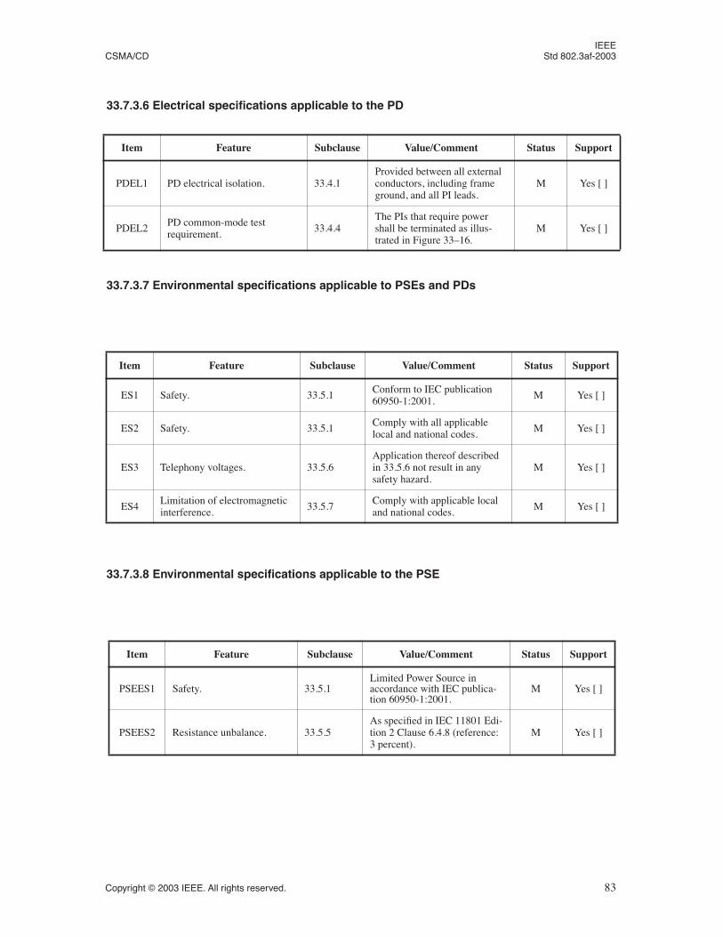
IEEE
CSMA/CD Std 802.3af-2003
33.7.3.6 Electrical specifications applicable to the PD
33.7.3.7 Environmental specifications applicable to PSEs and PDs
33.7.3.8 Environmental specifications applicable to the PSE
Item Feature Subclause Value/Comment Status Support
PDEL1 PD electrical isolation. 33.4.1Provided between all external conductors, including frame ground, and all PI leads.
M Yes [ ]
PDEL2 PD common-mode test requirement. 33.4.4
The PIs that require power shall be terminated as illus-trated in Figure 33–16.
M Yes [ ]
Item Feature Subclause Value/Comment Status Support
ES1 Safety. 33.5.1 Conform to IEC publication 60950-1:2001. M Yes [ ]
ES2 Safety. 33.5.1 Comply with all applicable local and national codes. M Yes [ ]
ES3 Telephony voltages. 33.5.6Application thereof described in 33.5.6 not result in any safety hazard.
M Yes [ ]
ES4 Limitation of electromagnetic interference. 33.5.7 Comply with applicable local
and national codes. M Yes [ ]
Item Feature Subclause Value/Comment Status Support
PSEES1 Safety. 33.5.1Limited Power Source in accordance with IEC publica-tion 60950-1:2001.
M Yes [ ]
PSEES2 Resistance unbalance. 33.5.5As specified in IEC 11801 Edi-tion 2 Clause 6.4.8 (reference: 3 percent).
M Yes [ ]
Copyright © 2003 IEEE. All rights reserved. 83
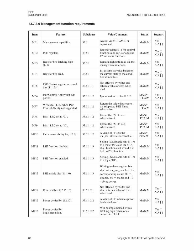
IEEE Std 802.3af-2003 AMENDMENT TO IEEE Std 802.3
33.7.3.9 Management function requirements
Item Feature Subclause Value/Comment Status Support
MF1 Management capability. 33.6 Access via MII, GMII, or equivalent. MAN:M Yes [ ]
N/A [ ]
MF2 PSE registers. 33.6.1Register address 11 for control functions and register address 12 for status functions.
MAN:M Yes [ ]N/A [ ]
MF3 Register bits latching high
(LH).33.6.1 Remain high until read via the
management interface. MAN:M Yes [ ]N/A [ ]
MF4 Register bits read. 33.6.1Bit assumes a value based on the current state of the condi-tion it monitors.
MAN:M Yes [ ]N/A [ ]
MF5 PSE Control register reserved bits (11.15:4). 33.6.1.1.1
Not affected by writes and return a value of zero when read.
MAN:M Yes [ ]N/A [ ]
MF6 Pair Control Ability not sup-ported. 33.6.1.1.2 Ignore writes to bits 11.3:2. MAN∗
!PCA:MYes [ ]N/A [ ]
MF7 Writes to 11.3:2 when Pair Control Ability not supported. 33.6.1.1.2
Return the value that reports the supported PSE Pinout Alternative.
MAN∗!PCA:M
Yes [ ]N/A [ ]
MF8 Bits 11.3:2 set to '01'. 33.6.1.1.2 Forces the PSE to use Alternative A.
MAN∗PCA:M
Yes [ ]N/A [ ]
MF9 Bits 11.3:2 set to '10'. 33.6.1.1.2 Forces the PSE to use Alternative B.
MAN∗PCA:M
Yes [ ]N/A [ ]
MF10 Pair control ability bit, (12.0). 33.6.1.1.2 A value of ‘1’ sets the mr_pse_alternative variable.
MAN∗PCA:M
Yes [ ]N/A [ ]
MF11 PSE function disabled 33.6.1.1.3
Setting PSE Enable bits 11.1:0 to a logic ‘00’, also the MDI
shall function as it would if it
had no PSE function.
MAN:M Yes [ ]N/A [ ]
MF12 PSE function enabled. 33.6.1.1.3 Setting PSE Enable bits 11.1:0 to a logic ‘01’. MAN:M Yes [ ]
N/A [ ]
MF13 PSE enable bits (11.1:0). 33.6.1.1.3
Writing to these register bits
shall set mr_pse_enable to the
corresponding value: 00 =
disable, 01 = enable and 10
= force power.
MAN:M Yes [ ]N/A [ ]
MF14 Reserved bits (12.15:13). 33.6.1.2.1Not affected by writes and shall return a value of zero when read.
MAN:M Yes [ ]N/A [ ]
MF15 Power denied bit (12.12). 33.6.1.2.2 A value of ‘1’ indicates power has been denied. MAN:M Yes [ ]
N/A [ ]
MF16 Power denied bit implementation. 33.6.1.2.2
Will be implemented with a latching high behavior as defined in 33.6.1.
MAN:M Yes [ ]N/A [ ]
84 Copyright © 2003 IEEE. All rights reserved.
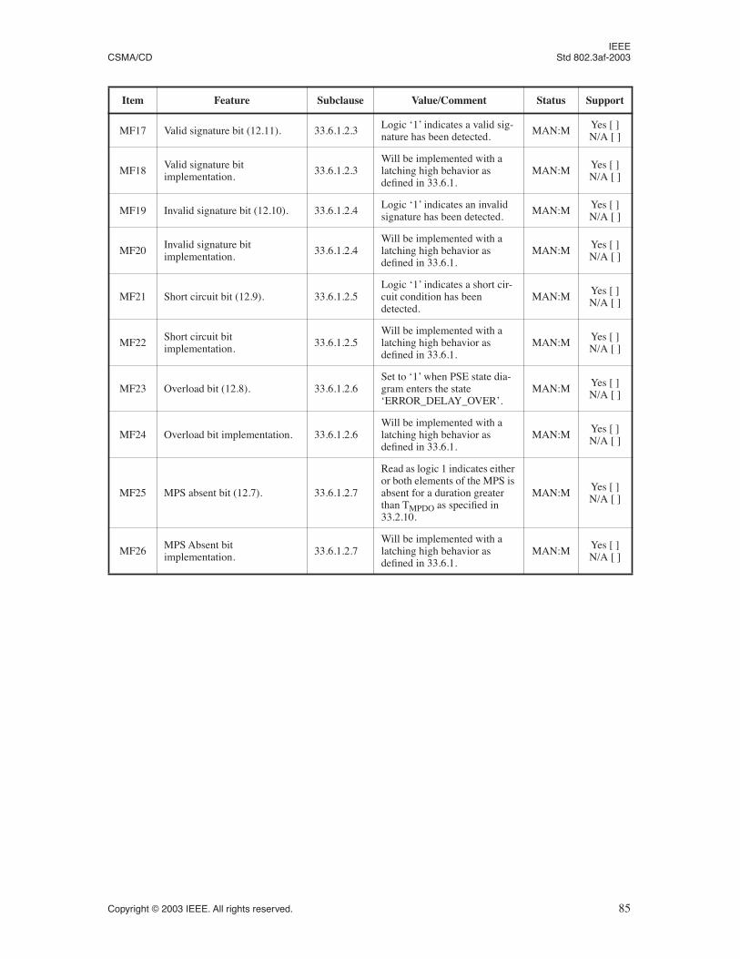
IEEE CSMA/CD Std 802.3af-2003
MF17 Valid signature bit (12.11). 33.6.1.2.3 Logic ‘1’ indicates a valid sig-nature has been detected. MAN:M Yes [ ]
N/A [ ]
MF18 Valid signature bit implementation. 33.6.1.2.3
Will be implemented with a latching high behavior as defined in 33.6.1.
MAN:M Yes [ ]N/A [ ]
MF19 Invalid signature bit (12.10). 33.6.1.2.4 Logic ‘1’ indicates an invalid signature has been detected. MAN:M Yes [ ]
N/A [ ]
MF20 Invalid signature bit implementation. 33.6.1.2.4
Will be implemented with a latching high behavior as defined in 33.6.1.
MAN:M Yes [ ]N/A [ ]
MF21 Short circuit bit (12.9). 33.6.1.2.5Logic ‘1’ indicates a short cir-cuit condition has been detected.
MAN:M Yes [ ]N/A [ ]
MF22 Short circuit bit implementation. 33.6.1.2.5
Will be implemented with a latching high behavior as defined in 33.6.1.
MAN:M Yes [ ]N/A [ ]
MF23 Overload bit (12.8). 33.6.1.2.6Set to ‘1’ when PSE state dia-gram enters the state ‘ERROR_DELAY_OVER’.
MAN:M Yes [ ]N/A [ ]
MF24 Overload bit implementation. 33.6.1.2.6Will be implemented with a latching high behavior as defined in 33.6.1.
MAN:M Yes [ ]N/A [ ]
MF25 MPS absent bit (12.7). 33.6.1.2.7
Read as logic 1 indicates either or both elements of the MPS is absent for a duration greater than TMPDO as specified in 33.2.10.
MAN:M Yes [ ]N/A [ ]
MF26 MPS Absent bit implementation. 33.6.1.2.7
Will be implemented with a latching high behavior as defined in 33.6.1.
MAN:M Yes [ ]N/A [ ]
Item Feature Subclause Value/Comment Status Support
Copyright © 2003 IEEE. All rights reserved. 85
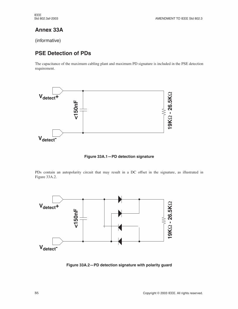
IEEE Std 802.3af-2003 AMENDMENT TO IEEE Std 802.3
Annex 33A
(informative)
PSE Detection of PDs
The capacitance of the maximum cabling plant and maximum PD signature is included in the PSE detectionrequirement.
PDs contain an autopolarity circuit that may result in a DC offset in the signature, as illustrated inFigure 33A.2.
Vdetect-
Vdetect+
<150
nF
19K
Ω -
26.
5KΩ
Figure 33A.1—PD detection signature
Vdetect-
Vdetect+
<150
nF
19K
Ω -
26.
5KΩ
Figure 33A.2—PD detection signature with polarity guard
86 Copyright © 2003 IEEE. All rights reserved.
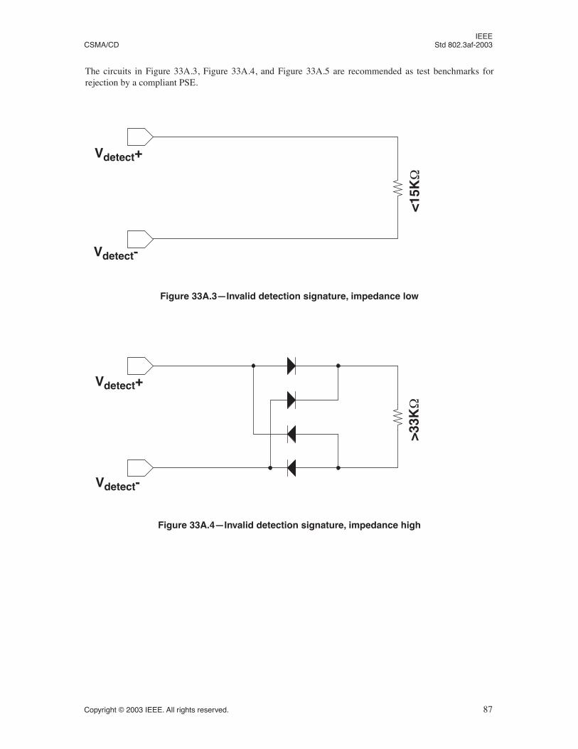
IEEE CSMA/CD Std 802.3af-2003
The circuits in Figure 33A.3, Figure 33A.4, and Figure 33A.5 are recommended as test benchmarks forrejection by a compliant PSE.
Vdetect-
Vdetect+
<15K
Ω
Figure 33A.3—Invalid detection signature, impedance low
Vdetect-
Vdetect+
>33K
Ω
Figure 33A.4—Invalid detection signature, impedance high
Copyright © 2003 IEEE. All rights reserved. 87
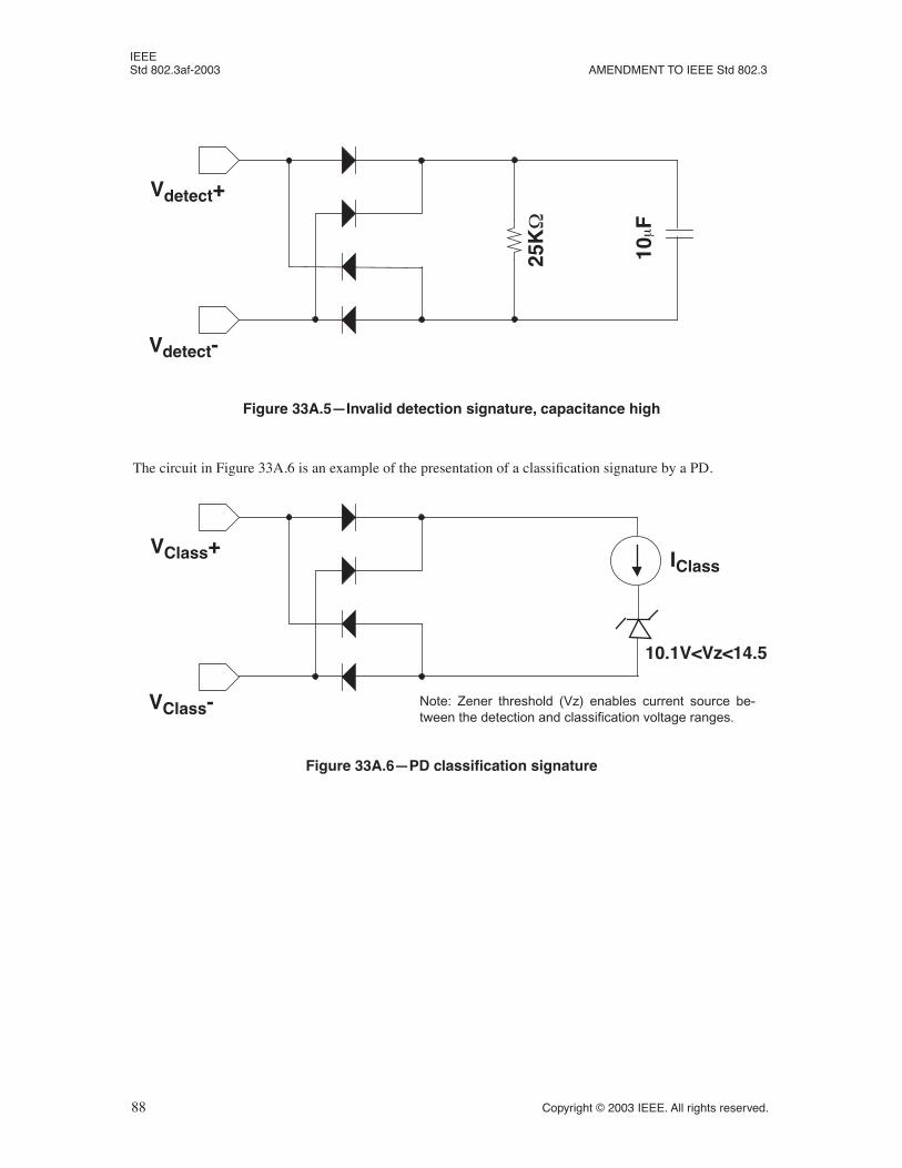
IEEE Std 802.3af-2003 AMENDMENT TO IEEE Std 802.3
The circuit in Figure 33A.6 is an example of the presentation of a classification signature by a PD.
Vdetect-
Vdetect+
25K
Ω
10µF
Figure 33A.5—Invalid detection signature, capacitance high
VClass-
VClass+IClass
10.1V<Vz<14.5
Note: Zener threshold (Vz) enables current source be-tween the detection and classification voltage ranges.
Figure 33A.6—PD classification signature
88 Copyright © 2003 IEEE. All rights reserved.
IEEE CSMA/CD Std 802.3af-2003
Annex 33B
(informative)
Cabling guidelines
DTE power via MDI is intended to operate over a 100 Ω balanced cabling infrastructure as described in ISO/IEC 11801-2000. Although initial implementations are expected to make use of Clause 33 to provide pow-ered IP telephones and wireless access points, Clause 33 is intended to address a much larger family of lowpower devices whose applications require connection to local area networks.
It is expected that in the future as building cabling infrastructures begin to support more building automationsystems (BAS), additional cabling guidelines will be implemented. BAS systems are used for controllingbuilding systems such as fire alarm, security, and access control (e.g., closed circuit television), and energymanagement systems (e.g., heating, ventilation, and air conditioning, and lighting control). One such stan-dard that is to be published to support these systems with a cabling infrastructure in EIA/TIA is the BuildingAutomation Cabling Standard for Commercial Buildings. This standard will specify a generic cablingsystem for building automation systems used in commercial buildings for a multi-product, multi-vendorenvironment. The purpose of the standard is to enable the planning and installation of a structured cablingsystem for building automation system applications that are required for use in new or renovated construc-tion of commercial buildings. It is significantly less expensive to integrate all of the major voice, data, andBAS applications by utilizing a fully-integrated structured cabling infrastructure.
For planning purposes, a sufficient number of horizontal cabling links should be provided for voice, data,and building automation services over the average floor space. It is recommended that a minimum of twooutlets be provided per work area as specified in the current standards in ISO/IEC.
Figure 33B.1—Figure
Copyright © 2003 IEEE. All rights reserved. 89
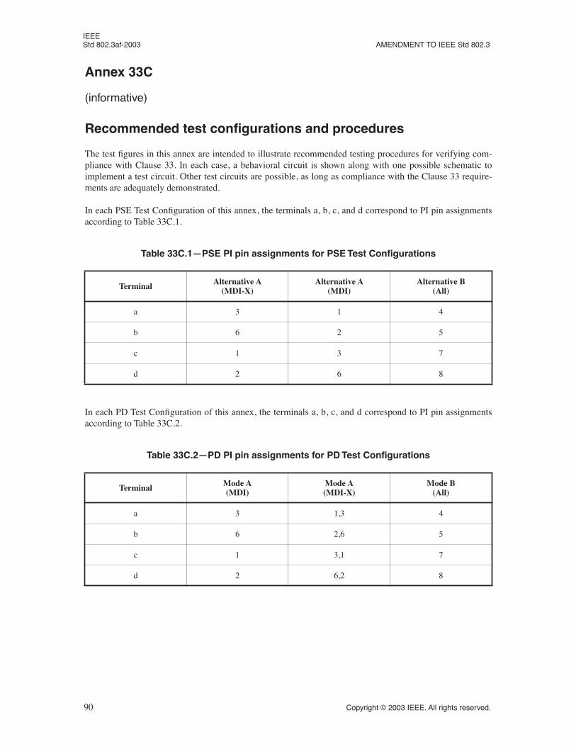
IEEE Std 802.3af-2003 AMENDMENT TO IEEE Std 802.3
Annex 33C
(informative)
Recommended test configurations and procedures
The test figures in this annex are intended to illustrate recommended testing procedures for verifying com-pliance with Clause 33. In each case, a behavioral circuit is shown along with one possible schematic toimplement a test circuit. Other test circuits are possible, as long as compliance with the Clause 33 require-ments are adequately demonstrated.
In each PSE Test Configuration of this annex, the terminals a, b, c, and d correspond to PI pin assignmentsaccording to Table 33C.1.
In each PD Test Configuration of this annex, the terminals a, b, c, and d correspond to PI pin assignmentsaccording to Table 33C.2.
Table 33C.1—PSE PI pin assignments for PSE Test Configurations
Terminal Alternative A(MDI-X)
Alternative A(MDI)
Alternative B(All)
a 3 1 4
b 6 2 5
c 1 3 7
d 2 6 8
Table 33C.2—PD PI pin assignments for PD Test Configurations
Terminal Mode A(MDI)
Mode A(MDI-X)
Mode B(All)
a 3 1,3 4
b 6 2,6 5
c 1 3,1 7
d 2 6,2 8
90 Copyright © 2003 IEEE. All rights reserved.
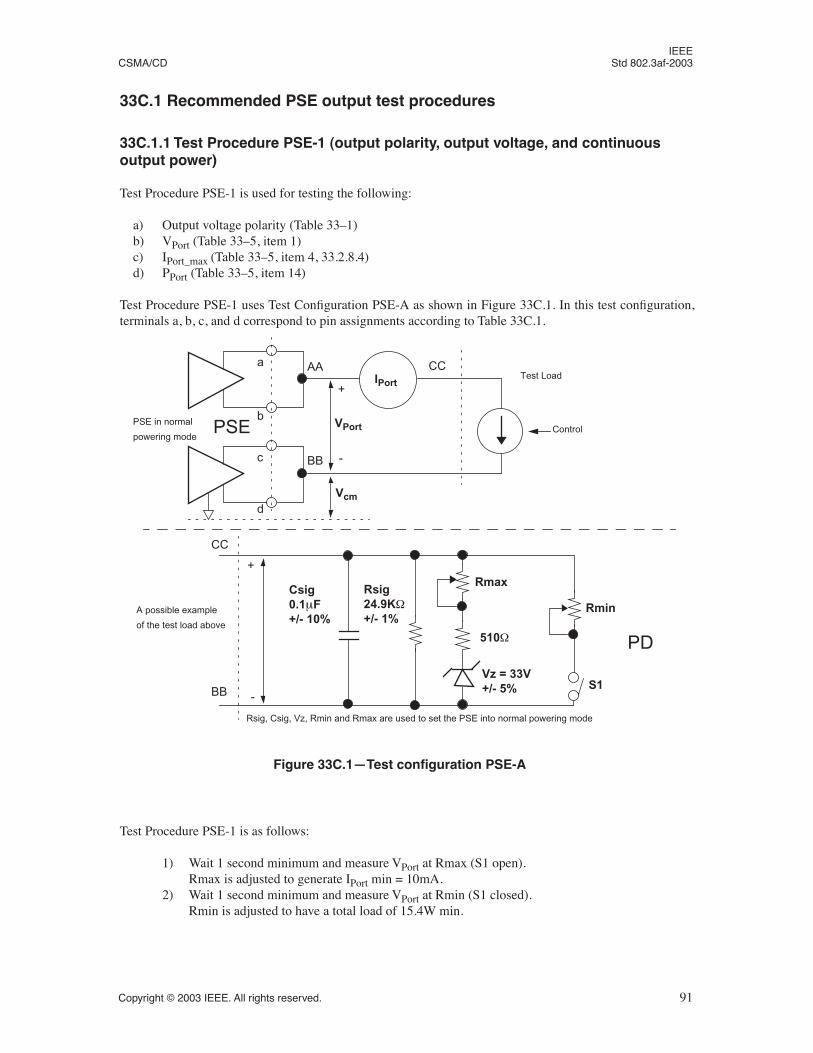
IEEE CSMA/CD Std 802.3af-2003
33C.1 Recommended PSE output test procedures
33C.1.1 Test Procedure PSE-1 (output polarity, output voltage, and continuous output power)
Test Procedure PSE-1 is used for testing the following:
a) Output voltage polarity (Table 33–1) b) VPort (Table 33–5, item 1)c) IPort_max (Table 33–5, item 4, 33.2.8.4)d) PPort (Table 33–5, item 14)
Test Procedure PSE-1 uses Test Configuration PSE-A as shown in Figure 33C.1. In this test configuration,terminals a, b, c, and d correspond to pin assignments according to Table 33C.1.
Test Procedure PSE-1 is as follows:
1) Wait 1 second minimum and measure VPort at Rmax (S1 open).Rmax is adjusted to generate IPort min = 10mA.
2) Wait 1 second minimum and measure VPort at Rmin (S1 closed).Rmin is adjusted to have a total load of 15.4W min.
Figure 33C.1—Test configuration PSE-A
PSE in normal
powering mode
a
c
b
d
A possible example
of the test load above
AA
BB
CC
+
-
VPort
IPortTest Load
Vcm
Control
+
-
Csig0.1µF+/- 10%
Rsig24.9KΩ+/- 1%
Rmax
510Ω
Rmin
S1Vz = 33V+/- 5%
Rsig, Csig, Vz, Rmin and Rmax are used to set the PSE into normal powering mode
CC
BB
PD
PSE
Copyright © 2003 IEEE. All rights reserved. 91
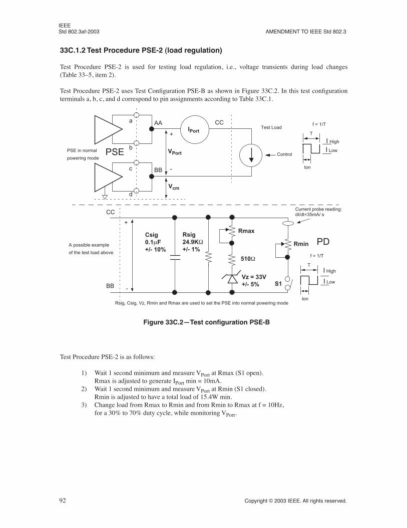
IEEE Std 802.3af-2003 AMENDMENT TO IEEE Std 802.3
33C.1.2 Test Procedure PSE-2 (load regulation)
Test Procedure PSE-2 is used for testing load regulation, i.e., voltage transients during load changes(Table 33–5, item 2).
Test Procedure PSE-2 uses Test Configuration PSE-B as shown in Figure 33C.2. In this test configurationterminals a, b, c, and d correspond to pin assignments according to Table 33C.1.
Test Procedure PSE-2 is as follows:
1) Wait 1 second minimum and measure VPort at Rmax (S1 open).Rmax is adjusted to generate IPort min = 10mA.
2) Wait 1 second minimum and measure VPort at Rmin (S1 closed).Rmin is adjusted to have a total load of 15.4W min.
3) Change load from Rmax to Rmin and from Rmin to Rmax at f = 10Hz,for a 30% to 70% duty cycle, while monitoring VPort.
Figure 33C.2—Test configuration PSE-B
PSE in normal
powering mode
a
c
b
d
A possible example
of the test load above
AA
BB
CC
+
-
VPort
IPortTest Load
Vcm
Control
+
-
Csig0.1µF+/- 10%
Rsig24.9KΩ+/- 1%
Rmax
510Ω
Rmin
S1Vz = 33V+/- 5%
Rsig, Csig, Vz, Rmin and Rmax are used to set the PSE into normal powering mode
CC
BB
PD
ton
T
f = 1/T
I High
I Low
ton
T
f = 1/T
I Low
I High
Current probe reading:dI/dt<35mA/ s
PSE
92 Copyright © 2003 IEEE. All rights reserved.
IEEE CSMA/CD Std 802.3af-2003
33C.1.3 Test Procedure PSE-3 (ripple and noise)
Test Procedure PSE-3 is used for testing ripple and noise (Table 33–5, item 3), 33.4.5 and 33.4.6.
Test Procedure PSE-3 uses Test Configuration PSE-A as shown in Figure 33C.1. In this test configurationterminals a, b, c, and d correspond to pin assignments according to Table 33C.1.
Test Procedure PSE-3 is as follows:
1) Wait 1 second minimum and measure VPort at Rmax (S1 open).Rmax is adjusted to generate IPort min = 10mA.
2) Wait 1 second minimum and measure VPort at Rmin (S1 closed).Rmin is adjusted to have a total load of 15.4W min.
3) Measure VPort ac noise and ripple at Rmax (S1 open) and at Rmin (S1 closed) by using spec-trum analyzer or equivalent equipment.
33C.1.4 Test Procedure PSE-4 (output current in startup mode)
Test Procedure PSE-4 is used for testing the following:
a) IInrush (Table 33–5, item 5) andb) TLIM (Table 33–5, item 11).
Copyright © 2003 IEEE. All rights reserved. 93
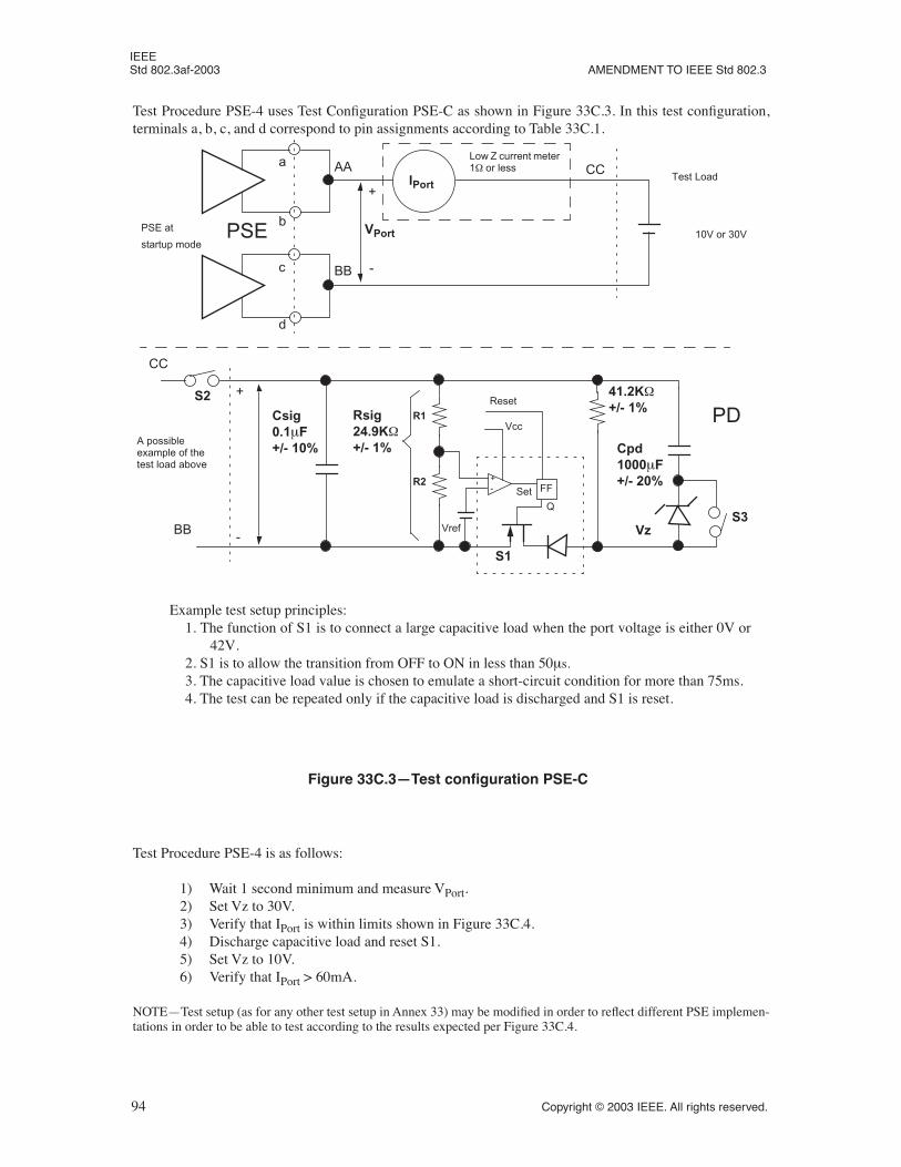
IEEE Std 802.3af-2003 AMENDMENT TO IEEE Std 802.3
Test Procedure PSE-4 uses Test Configuration PSE-C as shown in Figure 33C.3. In this test configuration,terminals a, b, c, and d correspond to pin assignments according to Table 33C.1.
Test Procedure PSE-4 is as follows:
1) Wait 1 second minimum and measure VPort.2) Set Vz to 30V.3) Verify that IPort is within limits shown in Figure 33C.4.4) Discharge capacitive load and reset S1.5) Set Vz to 10V.6) Verify that IPort > 60mA.
NOTE—Test setup (as for any other test setup in Annex 33) may be modified in order to reflect different PSE implemen-tations in order to be able to test according to the results expected per Figure 33C.4.
Figure 33C.3—Test configuration PSE-C
Example test setup principles:1. The function of S1 is to connect a large capacitive load when the port voltage is either 0V or
42V.2. S1 is to allow the transition from OFF to ON in less than 50µs.3. The capacitive load value is chosen to emulate a short-circuit condition for more than 75ms.4. The test can be repeated only if the capacitive load is discharged and S1 is reset.
PSE at
startup mode
a
c
b
d
AA
BB
CC
+
-
VPort
IPortTest Load
PSE 10V or 30V
Low Z current meter1Ω or less
A possible example of thetest load above
+
-
Csig0.1µF+/- 10%
Rsig24.9KΩ+/- 1%
S3
CC
BB
PDS2
R1
R2
Cpd1000µF+/- 20%
Vz
41.2KΩ+/- 1%
QSet FF
+-
Vref
Vcc
Reset
S1
94 Copyright © 2003 IEEE. All rights reserved.
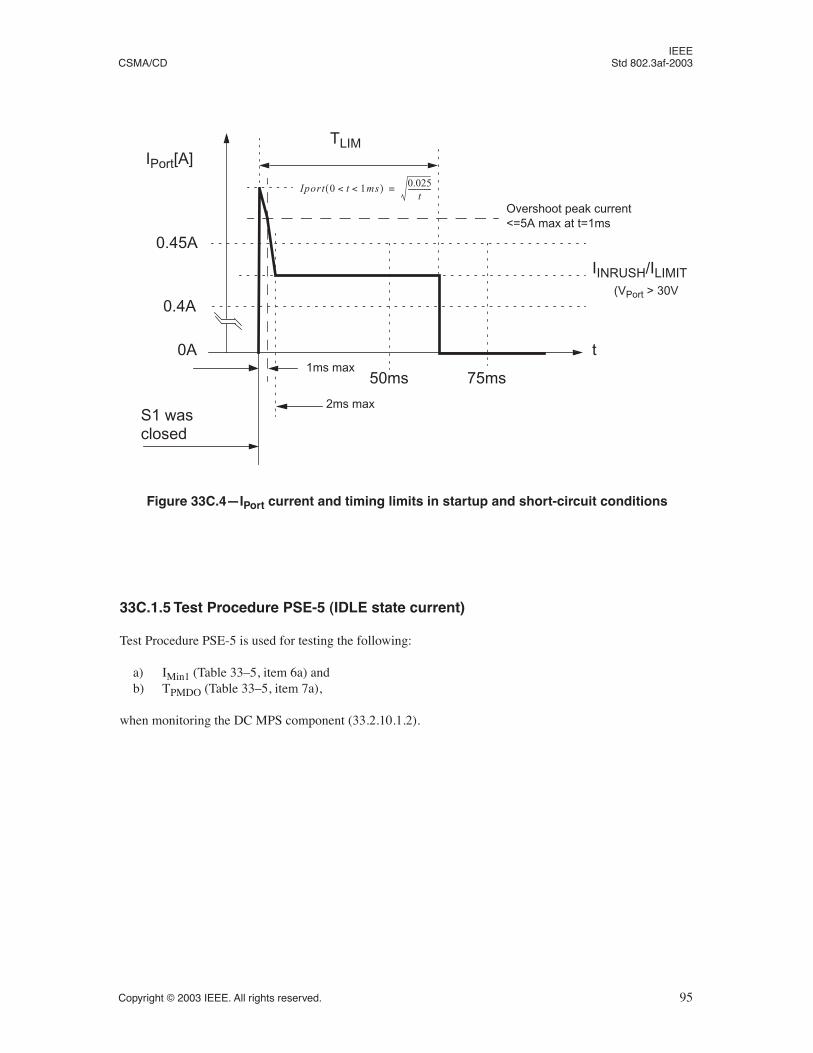
IEEE CSMA/CD Std 802.3af-2003
33C.1.5 Test Procedure PSE-5 (IDLE state current)
Test Procedure PSE-5 is used for testing the following:
a) IMin1 (Table 33–5, item 6a) andb) TPMDO (Table 33–5, item 7a),
when monitoring the DC MPS component (33.2.10.1.2).
Figure 33C.4—IPort current and timing limits in startup and short-circuit conditions
0A
0.4A
0.45A
IPort[A]
S1 wasclosed
TLIM
IINRUSH/ILIMIT
1ms max
2ms max
50ms 75ms
Overshoot peak current<=5A max at t=1ms
Iport 0 t 1ms< <( ) 0.025
t-------------=
t
(VPort > 30V
Copyright © 2003 IEEE. All rights reserved. 95
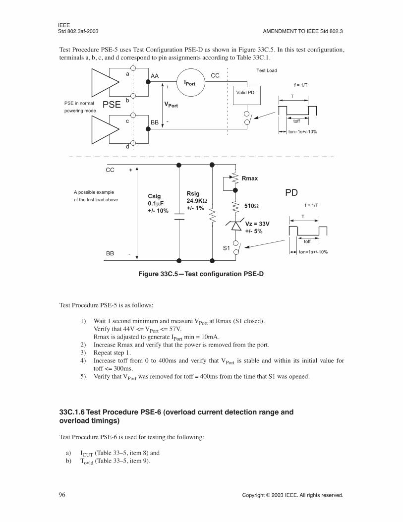
IEEE Std 802.3af-2003 AMENDMENT TO IEEE Std 802.3
Test Procedure PSE-5 uses Test Configuration PSE-D as shown in Figure 33C.5. In this test configuration,terminals a, b, c, and d correspond to pin assignments according to Table 33C.1.
Test Procedure PSE-5 is as follows:
1) Wait 1 second minimum and measure VPort at Rmax (S1 closed).Verify that 44V <= VPort <= 57V.Rmax is adjusted to generate IPort min = 10mA.
2) Increase Rmax and verify that the power is removed from the port.3) Repeat step 1.4) Increase toff from 0 to 400ms and verify that VPort is stable and within its initial value for
toff <= 300ms.5) Verify that VPort was removed for toff = 400ms from the time that S1 was opened.
33C.1.6 Test Procedure PSE-6 (overload current detection range and overload timings)
Test Procedure PSE-6 is used for testing the following:
a) ICUT (Table 33–5, item 8) andb) Tovld (Table 33–5, item 9).
Figure 33C.5—Test configuration PSE-D
PSE in normal
powering mode
a
c
b
d
AA
BB
CC
+
-
VPort
IPort
Test Load
ton=1s+/-10%
T
f = 1/T
PSE
Valid PD
toff
A possible example
of the test load above
+
-
Csig0.1µF+/- 10%
Rsig24.9KΩ+/- 1%
Rmax
510Ω
Vz = 33V+/- 5%
CC
BB ton=1s+/-10%
T
f = 1/T
toff
S1
PD
96 Copyright © 2003 IEEE. All rights reserved.
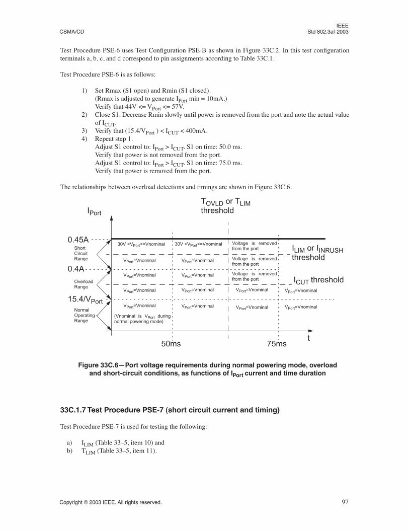
IEEE CSMA/CD Std 802.3af-2003
Test Procedure PSE-6 uses Test Configuration PSE-B as shown in Figure 33C.2. In this test configurationterminals a, b, c, and d correspond to pin assignments according to Table 33C.1.
Test Procedure PSE-6 is as follows:
1) Set Rmax (S1 open) and Rmin (S1 closed).(Rmax is adjusted to generate IPort min = 10mA.)Verify that 44V <= VPort <= 57V.
2) Close S1. Decrease Rmin slowly until power is removed from the port and note the actual valueof ICUT.
3) Verify that (15.4/VPort ) < ICUT < 400mA.4) Repeat step 1.
Adjust S1 control to: IPort > ICUT. S1 on time: 50.0 ms.Verify that power is not removed from the port.Adjust S1 control to: IPort > ICUT. S1 on time: 75.0 ms.Verify that power is removed from the port.
The relationships between overload detections and timings are shown in Figure 33C.6.
33C.1.7 Test Procedure PSE-7 (short circuit current and timing)
Test Procedure PSE-7 is used for testing the following:
a) ILIM (Table 33–5, item 10) andb) TLIM (Table 33–5, item 11).
Figure 33C.6—Port voltage requirements during normal powering mode, overload and short-circuit conditions, as functions of IPort current and time duration
0.45A
0.4A
15.4/VPort
50ms 75ms
TOVLD or TLIMthreshold
ILIM or IINRUSHthreshold
ICUT threshold
IPort
t
ShortCircuit Range
OverloadRange
NormalOperatingRange
VPort=Vnominal
VPort=Vnominal
VPort=Vnominal
30V <VPort<=Vnominal
(Vnominal is VPort duringnormal powering mode)
VPort=Vnominal VPort=Vnominal
VPort=Vnominal
VPort=Vnominal
VPort=Vnominal
VPort=Vnominal
VPort=Vnominal
Voltage is removedfrom the port
Voltage is removedfrom the port
Voltage is removedfrom the port
VPort=Vnominal
VPort=Vnominal
30V <VPort<=Vnominal
Copyright © 2003 IEEE. All rights reserved. 97
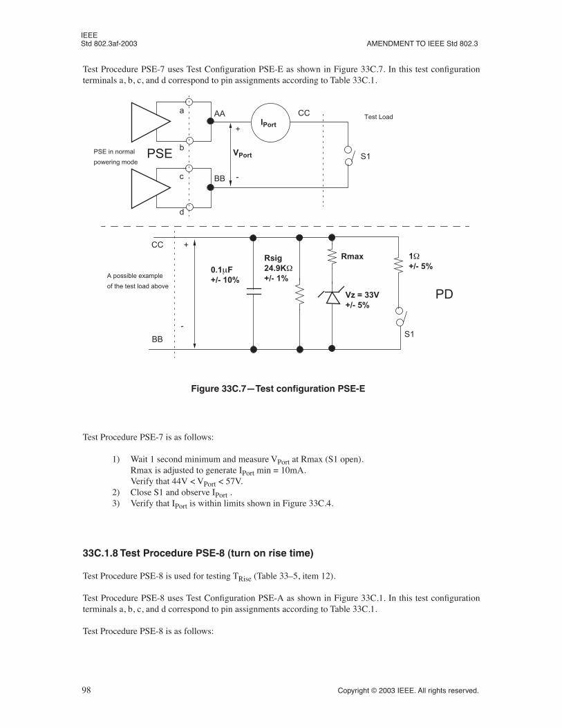
IEEE Std 802.3af-2003 AMENDMENT TO IEEE Std 802.3
Test Procedure PSE-7 uses Test Configuration PSE-E as shown in Figure 33C.7. In this test configurationterminals a, b, c, and d correspond to pin assignments according to Table 33C.1.
Test Procedure PSE-7 is as follows:
1) Wait 1 second minimum and measure VPort at Rmax (S1 open).Rmax is adjusted to generate IPort min = 10mA.Verify that 44V < VPort < 57V.
2) Close S1 and observe IPort .3) Verify that IPort is within limits shown in Figure 33C.4.
33C.1.8 Test Procedure PSE-8 (turn on rise time)
Test Procedure PSE-8 is used for testing TRise (Table 33–5, item 12).
Test Procedure PSE-8 uses Test Configuration PSE-A as shown in Figure 33C.1. In this test configurationterminals a, b, c, and d correspond to pin assignments according to Table 33C.1.
Test Procedure PSE-8 is as follows:
Figure 33C.7—Test configuration PSE-E
PSE in normal
powering mode
a
c
b
d
AA
BB
CC
+
-
VPort
IPortTest Load
PSE
A possible example
of the test load above
+
-
0.1µF+/- 10%
Rsig24.9KΩ+/- 1%
Rmax
Vz = 33V+/- 5%
CC
BBS1
PD
S1
1Ω+/- 5%
98 Copyright © 2003 IEEE. All rights reserved.
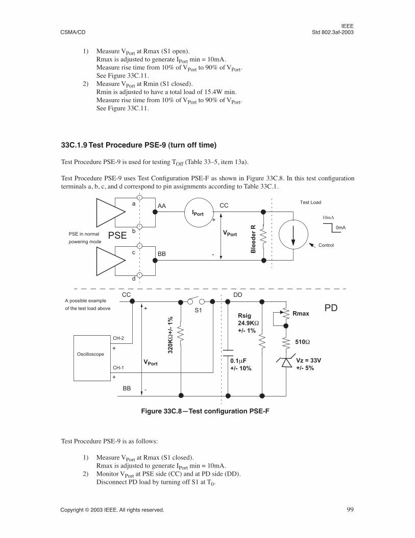
IEEE CSMA/CD Std 802.3af-2003
1) Measure VPort at Rmax (S1 open).Rmax is adjusted to generate IPort min = 10mA.Measure rise time from 10% of VPort to 90% of VPort.See Figure 33C.11.
2) Measure VPort at Rmin (S1 closed).Rmin is adjusted to have a total load of 15.4W min.Measure rise time from 10% of VPort to 90% of VPort.See Figure 33C.11.
33C.1.9 Test Procedure PSE-9 (turn off time)
Test Procedure PSE-9 is used for testing TOff (Table 33–5, item 13a).
Test Procedure PSE-9 uses Test Configuration PSE-F as shown in Figure 33C.8. In this test configurationterminals a, b, c, and d correspond to pin assignments according to Table 33C.1.
Test Procedure PSE-9 is as follows:
1) Measure VPort at Rmax (S1 closed).Rmax is adjusted to generate IPort min = 10mA.
2) Monitor VPort at PSE side (CC) and at PD side (DD).Disconnect PD load by turning off S1 at T0.
Figure 33C.8—Test configuration PSE-F
PSE in normal
powering mode
a
c
b
d
AA
BB
CC
+
-
VPort
IPort
Test Load
PSE
A possible example
of the test load above +
-
0.1µF+/- 10%
Rsig24.9KΩ+/- 1%
Rmax
510Ω
Vz = 33V+/- 5%
CC
BB
S1 PD
Ble
eder
RControl
10mA
0mA
Oscilloscope
VPort
320K
Ω+/
- 1%
DD
CH-1
CH-2
+
+
Copyright © 2003 IEEE. All rights reserved. 99
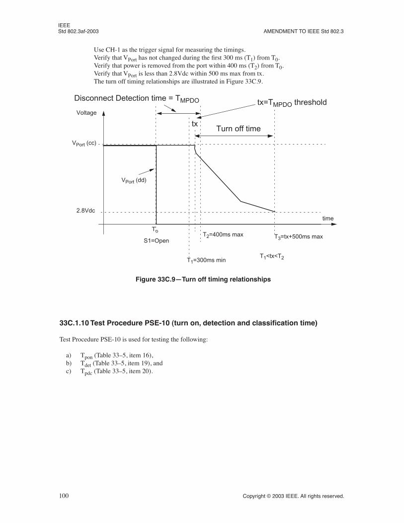
IEEE Std 802.3af-2003 AMENDMENT TO IEEE Std 802.3
Use CH-1 as the trigger signal for measuring the timings.Verify that VPort has not changed during the first 300 ms (T1) from T0.Verify that power is removed from the port within 400 ms (T2) from T0.Verify that VPort is less than 2.8Vdc within 500 ms max from tx.The turn off timing relationships are illustrated in Figure 33C.9.
33C.1.10 Test Procedure PSE-10 (turn on, detection and classification time)
Test Procedure PSE-10 is used for testing the following:
a) Tpon (Table 33–5, item 16),b) Tdet (Table 33–5, item 19), andc) Tpdc (Table 33–5, item 20).
Figure 33C.9—Turn off timing relationships
tx
tx=TMPDO thresholdDisconnect Detection time = TMPDO
Turn off time
VPort (cc)
VPort (dd)
2.8Vdc
Voltage
time
To
T1=300ms min
T2=400ms max T3=tx+500ms max
T1<tx<T2
S1=Open
100 Copyright © 2003 IEEE. All rights reserved.
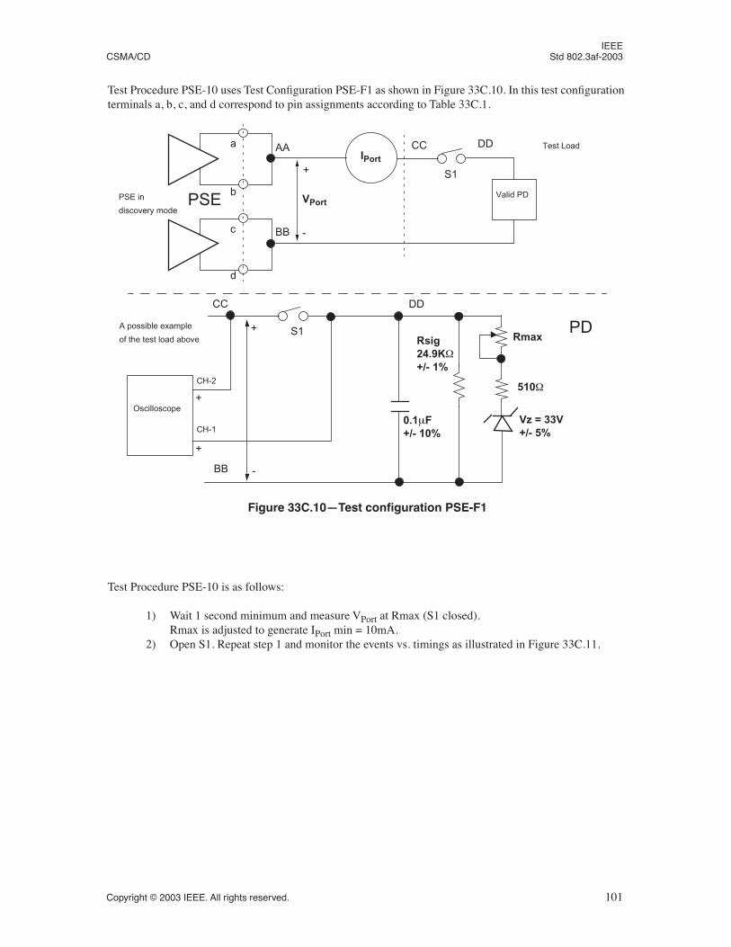
IEEE CSMA/CD Std 802.3af-2003
Test Procedure PSE-10 uses Test Configuration PSE-F1 as shown in Figure 33C.10. In this test configurationterminals a, b, c, and d correspond to pin assignments according to Table 33C.1.
Test Procedure PSE-10 is as follows:
1) Wait 1 second minimum and measure VPort at Rmax (S1 closed).Rmax is adjusted to generate IPort min = 10mA.
2) Open S1. Repeat step 1 and monitor the events vs. timings as illustrated in Figure 33C.11.
Figure 33C.10—Test configuration PSE-F1
PSE in
discovery mode
a
c
b
d
AA
BB
CC
+
-
VPort
IPort
Test Load
PSE
+
-
0.1µF+/- 10%
Rsig24.9KΩ+/- 1%
Rmax
510Ω
Vz = 33V+/- 5%
CC
BB
S1 PD
Oscilloscope
DD
DD
S1
Valid PD
CH-1
CH-2
+
+
A possible example
of the test load above
Copyright © 2003 IEEE. All rights reserved. 101
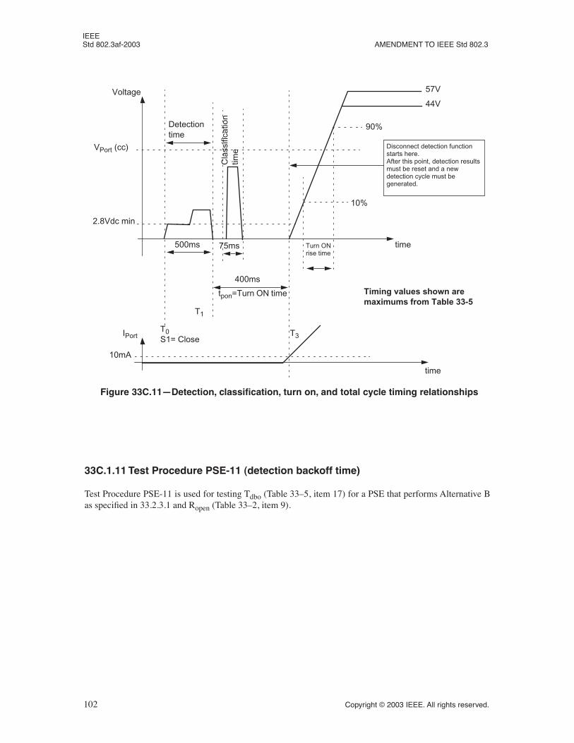
IEEE Std 802.3af-2003 AMENDMENT TO IEEE Std 802.3
33C.1.11 Test Procedure PSE-11 (detection backoff time)
Test Procedure PSE-11 is used for testing Tdbo (Table 33–5, item 17) for a PSE that performs Alternative Bas specified in 33.2.3.1 and Ropen (Table 33–2, item 9).
Figure 33C.11—Detection, classification, turn on, and total cycle timing relationships
VPort (cc)
Voltage
time
time
2.8Vdc min
Detectiontime
tpon=Turn ON time
Cla
ssifi
catio
n tim
e
57V
44V
90%
10%
500ms 75ms
400ms
Turn ONrise time
T1
T3T0S1= Close
IPort
10mA
Disconnect detection function starts here.After this point, detection resultsmust be reset and a newdetection cycle must begenerated.
Timing values shown aremaximums from Table 33-5
102 Copyright © 2003 IEEE. All rights reserved.
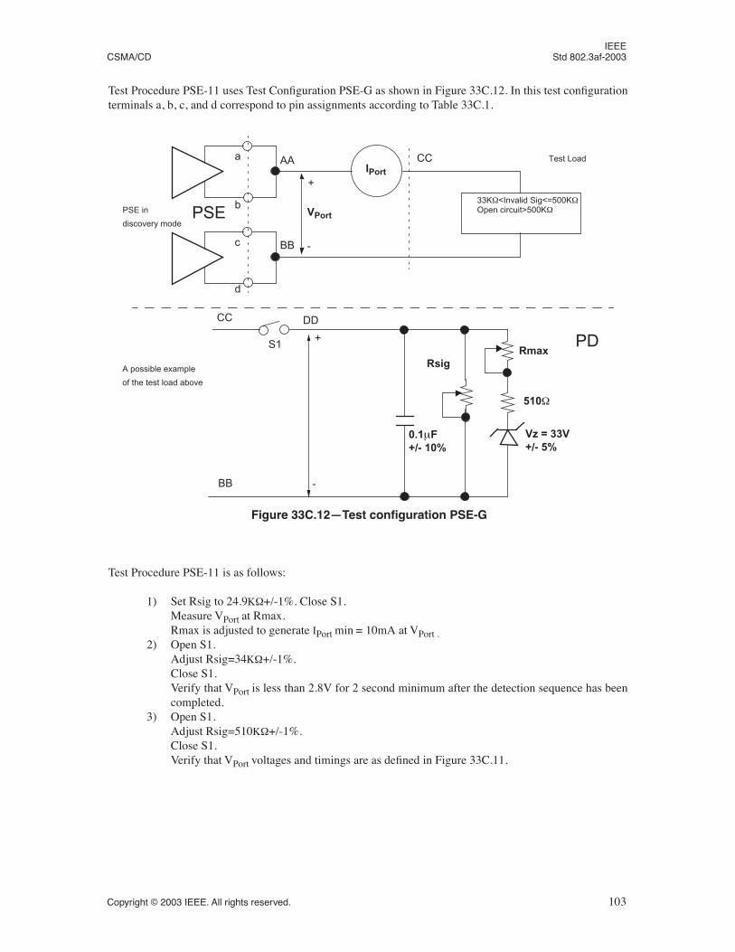
IEEE CSMA/CD Std 802.3af-2003
Test Procedure PSE-11 uses Test Configuration PSE-G as shown in Figure 33C.12. In this test configurationterminals a, b, c, and d correspond to pin assignments according to Table 33C.1.
Test Procedure PSE-11 is as follows:
1) Set Rsig to 24.9KΩ+/-1%. Close S1.Measure VPort at Rmax.Rmax is adjusted to generate IPort min = 10mA at VPort .
2) Open S1.Adjust Rsig=34KΩ+/-1%.Close S1.Verify that VPort is less than 2.8V for 2 second minimum after the detection sequence has beencompleted.
3) Open S1.Adjust Rsig=510KΩ+/-1%.Close S1.Verify that VPort voltages and timings are as defined in Figure 33C.11.
Figure 33C.12—Test configuration PSE-G
PSE in
discovery mode
a
c
b
d
AA
BB
CC
+
-
VPort
IPort
Test Load
PSE
+
-
0.1µF+/- 10%
RsigRmax
510Ω
Vz = 33V+/- 5%
CC
BB
S1 PD
33KΩ<Invalid Sig<=500KΩOpen circuit>500KΩ
A possible example
of the test load above
DD
Copyright © 2003 IEEE. All rights reserved. 103
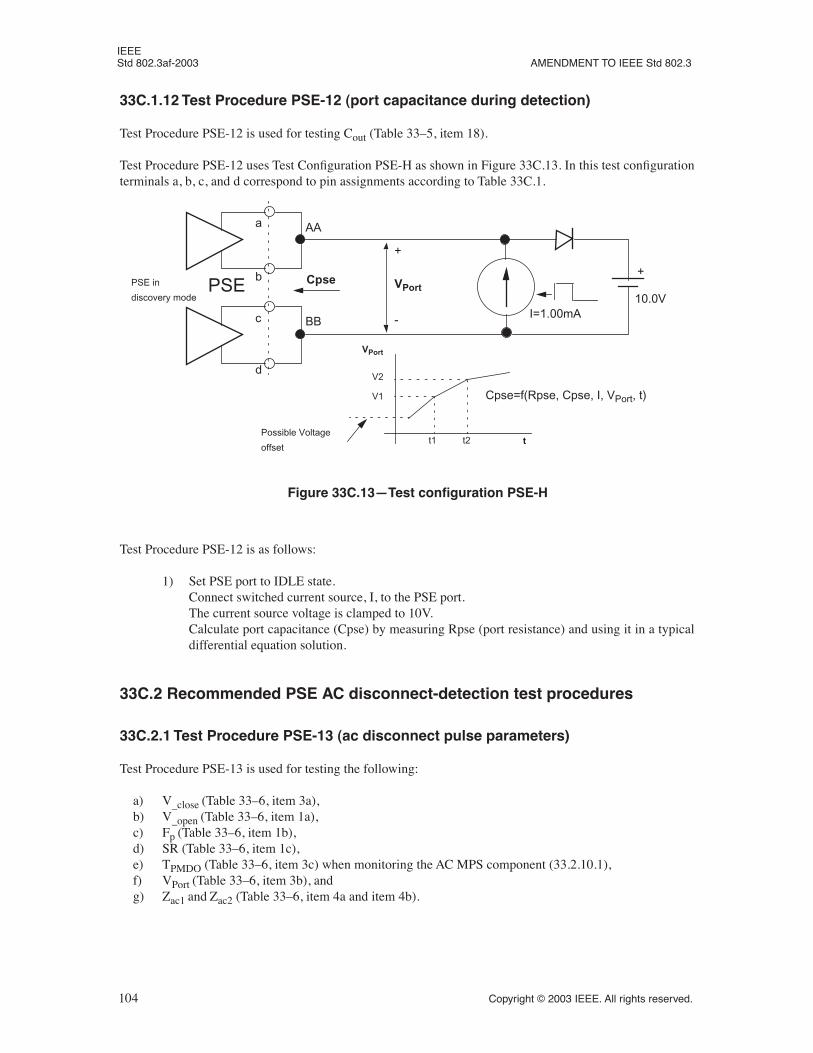
IEEE Std 802.3af-2003 AMENDMENT TO IEEE Std 802.3
33C.1.12 Test Procedure PSE-12 (port capacitance during detection)
Test Procedure PSE-12 is used for testing Cout (Table 33–5, item 18).
Test Procedure PSE-12 uses Test Configuration PSE-H as shown in Figure 33C.13. In this test configurationterminals a, b, c, and d correspond to pin assignments according to Table 33C.1.
Test Procedure PSE-12 is as follows:
1) Set PSE port to IDLE state.Connect switched current source, I, to the PSE port.The current source voltage is clamped to 10V.Calculate port capacitance (Cpse) by measuring Rpse (port resistance) and using it in a typicaldifferential equation solution.
33C.2 Recommended PSE AC disconnect-detection test procedures
33C.2.1 Test Procedure PSE-13 (ac disconnect pulse parameters)
Test Procedure PSE-13 is used for testing the following:
a) V_close (Table 33–6, item 3a),b) V_open (Table 33–6, item 1a),c) Fp (Table 33–6, item 1b),d) SR (Table 33–6, item 1c),e) TPMDO (Table 33–6, item 3c) when monitoring the AC MPS component (33.2.10.1),f) VPort (Table 33–6, item 3b), andg) Zac1 and Zac2 (Table 33–6, item 4a and item 4b).
Figure 33C.13—Test configuration PSE-H
PSE in
discovery mode
a
c
b
d
AA
BB
+
-
VPortPSE
VPort
tPossible Voltage
offset
V2
t2
V1
t1
Cpse=f(Rpse, Cpse, I, VPort, t)
Cpse
I=1.00mA
+
10.0V
104 Copyright © 2003 IEEE. All rights reserved.
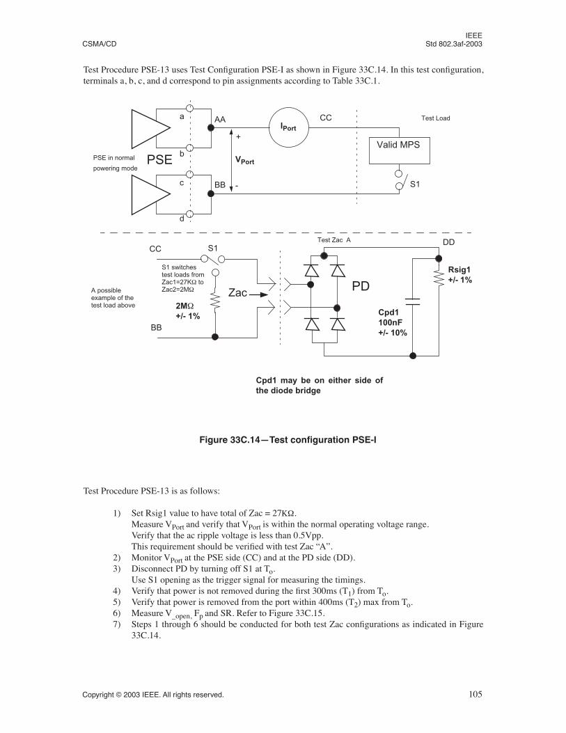
IEEE CSMA/CD Std 802.3af-2003
Test Procedure PSE-13 uses Test Configuration PSE-I as shown in Figure 33C.14. In this test configuration,terminals a, b, c, and d correspond to pin assignments according to Table 33C.1.
Test Procedure PSE-13 is as follows:
1) Set Rsig1 value to have total of Zac = 27KΩ.Measure VPort and verify that VPort is within the normal operating voltage range.Verify that the ac ripple voltage is less than 0.5Vpp.This requirement should be verified with test Zac “A”.
2) Monitor VPort at the PSE side (CC) and at the PD side (DD).3) Disconnect PD by turning off S1 at To.
Use S1 opening as the trigger signal for measuring the timings.4) Verify that power is not removed during the first 300ms (T1) from To.5) Verify that power is removed from the port within 400ms (T2) max from To.6) Measure V_open, Fp and SR. Refer to Figure 33C.15.7) Steps 1 through 6 should be conducted for both test Zac configurations as indicated in Figure
33C.14.
Figure 33C.14—Test configuration PSE-I
PSE in normal
powering mode
a
c
b
d
AA
BB
CC
+
-
VPort
IPort
Test Load
PSEValid MPS
S1
S1
A possibleexample of thetest load above
CC
BB
S1 switchestest loads fromZac1=27KΩ toZac2=2MΩ
2MΩ+/- 1%
Zac PD
Cpd1100nF+/- 10%
Rsig1+/- 1%
DDTest Zac A
Cpd1 may be on either side ofthe diode bridge
Copyright © 2003 IEEE. All rights reserved. 105
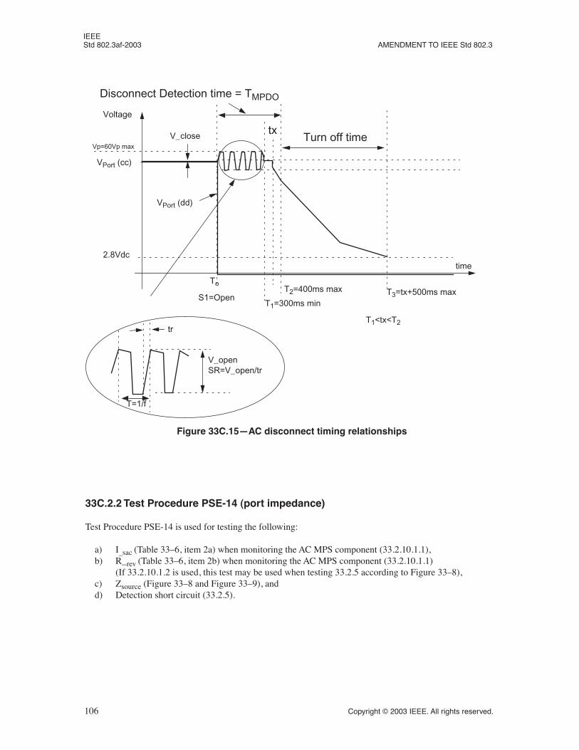
IEEE Std 802.3af-2003 AMENDMENT TO IEEE Std 802.3
33C.2.2 Test Procedure PSE-14 (port impedance)
Test Procedure PSE-14 is used for testing the following:
a) I_sac (Table 33–6, item 2a) when monitoring the AC MPS component (33.2.10.1.1),b) R_rev (Table 33–6, item 2b) when monitoring the AC MPS component (33.2.10.1.1)
(If 33.2.10.1.2 is used, this test may be used when testing 33.2.5 according to Figure 33–8),c) Zsource (Figure 33–8 and Figure 33–9), andd) Detection short circuit (33.2.5).
Figure 33C.15—AC disconnect timing relationships
tx
Disconnect Detection time = TMPDO
Turn off time
VPort (cc)
VPort (dd)
2.8Vdc
Voltage
time
To
T1=300ms min
T2=400ms max T3=tx+500ms max
T1<tx<T2
S1=Open
Vp=60Vp max
V_close
tr
T=1/f
V_openSR=V_open/tr
106 Copyright © 2003 IEEE. All rights reserved.
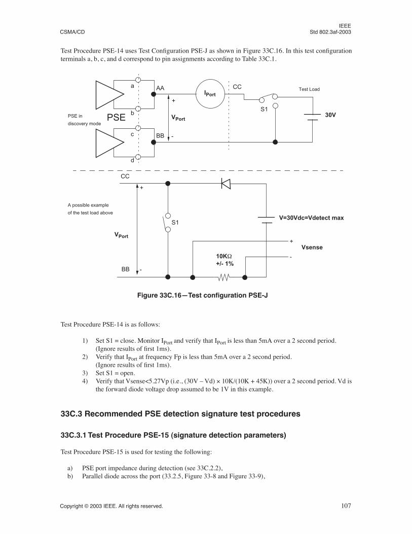
IEEE CSMA/CD Std 802.3af-2003
Test Procedure PSE-14 uses Test Configuration PSE-J as shown in Figure 33C.16. In this test configurationterminals a, b, c, and d correspond to pin assignments according to Table 33C.1.
Test Procedure PSE-14 is as follows:
1) Set S1 = close. Monitor IPort and verify that IPort is less than 5mA over a 2 second period.(Ignore results of first 1ms).
2) Verify that IPort at frequency Fp is less than 5mA over a 2 second period.(Ignore results of first 1ms).
3) Set S1 = open.4) Verify that Vsense<5.27Vp (i.e., (30V – Vd) × 10K/(10K + 45K)) over a 2 second period. Vd is
the forward diode voltage drop assumed to be 1V in this example.
33C.3 Recommended PSE detection signature test procedures
33C.3.1 Test Procedure PSE-15 (signature detection parameters)
Test Procedure PSE-15 is used for testing the following:
a) PSE port impedance during detection (see 33C.2.2),b) Parallel diode across the port (33.2.5, Figure 33-8 and Figure 33-9),
Figure 33C.16—Test configuration PSE-J
PSE in
discovery mode
a
c
b
d
AA
BB
CC
+
-
VPort
IPortTest Load
PSE
+
-
10KΩ+/- 1%
CC
BB
S1
VPort
A possible example
of the test load above
S130V
V=30Vdc=Vdetect max
Vsense+
-
Copyright © 2003 IEEE. All rights reserved. 107
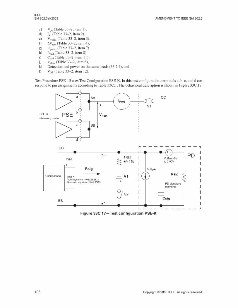
IEEE Std 802.3af-2003 AMENDMENT TO IEEE Std 802.3
c) Voc (Table 33–2, item 1),d) Isc (Table 33–2, item 2),e) Vvalid (Table 33–2, item 3),f) ∆Vtest (Table 33–2, item 4),g) Rgood, (Table 33–2, item 7)h) Rbad (Table 33–2, item 8),i) Cbad (Table 33–2, item 11),j) Vslew (Table 33–2, item 6),k) Detection and power on the same leads (33.2.4), andl) VOS (Table 33–2, item 12).
Test Procedure PSE-15 uses Test Configuration PSE-K. In this test configuration, terminals a, b, c, and d cor-respond to pin assignments according to Table 33C.1. The behavioral description is shown in Figure 33C.17.
Figure 33C.17—Test configuration PSE-K
PSE in
discovery mode
a
c
b
d
AA
BB
CC
+
-
VPort
IPort
PSE
S1
+
-
1KΩ+/- 1%
Rsig
CC
BB
PD
Oscilloscope
CH-1
+
+ -
V1
S2
0-12µA
Voffset=0Vto 2.00V
Rsig
Csig
PD signatureelements
Rsig =Valid signature: 19KΩ,26.5KΩNon-valid signature:15KΩ,33KΩ +
108 Copyright © 2003 IEEE. All rights reserved.
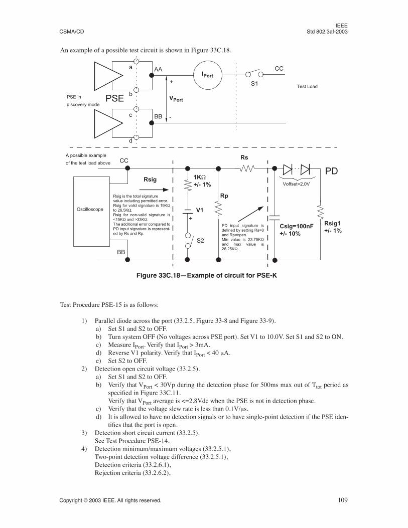
IEEE CSMA/CD Std 802.3af-2003
An example of a possible test circuit is shown in Figure 33C.18.
Test Procedure PSE-15 is as follows:
1) Parallel diode across the port (33.2.5, Figure 33-8 and Figure 33-9).a) Set S1 and S2 to OFF.b) Turn system OFF (No voltages across PSE port). Set V1 to 10.0V. Set S1 and S2 to ON.c) Measure IPort. Verify that IPort > 3mA.d) Reverse V1 polarity. Verify that IPort < 40 µA.e) Set S2 to OFF.
2) Detection open circuit voltage (33.2.5).a) Set S1 and S2 to OFF.b) Verify that VPort < 30Vp during the detection phase for 500ms max out of Ttot period as
specified in Figure 33C.11.Verify that VPort average is <=2.8Vdc when the PSE is not in detection phase.
c) Verify that the voltage slew rate is less than 0.1V/µs.d) It is allowed to have no detection signals or to have single-point detection if the PSE iden-
tifies that the port is open.3) Detection short circuit current (33.2.5).
See Test Procedure PSE-14.4) Detection minimum/maximum voltages (33.2.5.1),
Two-point detection voltage difference (33.2.5.1),Detection criteria (33.2.6.1),Rejection criteria (33.2.6.2),
Figure 33C.18—Example of circuit for PSE-K
PSE in
discovery mode
a
c
b
d
AA
BB
CC
+
-
VPort
IPort
PSE
S1
1KΩ+/- 1%
Rsig
CC
BB
PD
Oscilloscope V1
S2
Rsig1+/- 1%
Csig=100nF+/- 10%
Rsig is the total signaturevalue including permitted error.Rsig for valid signature is 19KΩto 26.5KΩ.Rsig for non-valid signature is<15KΩ and >33KΩ.The additional error compared toPD input signature is represent-ed by Rs and Rp.
+
Test Load
A possible example
of the test load above
Rp
Rs
Voffset=2.0V
PD input signature isdefined by setting Rs=0and Rp=open.Min value is 23.75KΩand max value is26.25KΩ.
Copyright © 2003 IEEE. All rights reserved. 109
IEEE Std 802.3af-2003 AMENDMENT TO IEEE Std 802.3
Detection voltage slew rate (33.2.5.1), andDetection and power on the same leads (33.2.5.1).a) Part 1.
i) Set Rs=0. Adjust VOFFSET to 0V.ii) Set Rsig1 to 23.75KΩ. Adjust Rsig to 19.0KΩ by adjusting Rp.iii) Adjust VOFFSET to 2.0V.
b) Part 2.i) Set S1 to ON. Set S2 to OFF.ii) Monitor VPort and measure detection voltages Vdet1 and Vdet2.
Verify that Vdet1 and Vdet2 are between 2.8V and 10V and |Vdet2 - Vdet1|>=1V.iii) Verify that 44V min is present across the port for 299ms min.iv) Verify that the slew rates of all the switched voltages are less than 0.1V/ µs.
c) Part 3.i) Adjust VOFFSET to 0V.ii) Set Rsig1 to 26.25KΩ. Set Rp=Open. Adjust Rsig to 26.5KΩ. by adjusting Rs.iii) Adjust VOFFSET to 2.0V.iv) Repeat step 4ii.
d) Part 4.i) Adjust VOFFSET to 0V.ii) Set Rs=0. Set Rp=open. Set Rsig1 to 14.7KΩ+/-1%.iii) Set S1 to ON. Set S2 to OFF.iv) Verify that power is not applied to the port.
e) Part 5.i) Adjust VOFFSET to 0V.ii) Set Rs=0. Set Rp=Open. Set Rsig1 to 34KΩ+/-1%.iii) Set S1 to ON. Set S2 to OFF.iv) Verify that power is not applied to the port.
f) Part 6.i) Set Rsig1 to 24.9KΩ. Set Rp=Open. Set Rsig=0. Set Csig=10.0µF.ii) Adjust VOFFSET to 2.0V.iii) Set S1 to ON. Set S2 to OFF.iv) Verify that power is not applied to the port.v) Repeat steps ii to v with Rsig1=open.
33C.4 Recommended PD detection signature test procedures
33C.4.1 Test Procedure SIG-1 (PD signature characteristics)
Test Procedure SIG-1 is used for testing the following:
a) V-I slope (Table 33–8),b) V offset (Table 33–8),c) Input capacitance (Table 33–8), andd) PD classification current (Table 33–11).
110 Copyright © 2003 IEEE. All rights reserved.
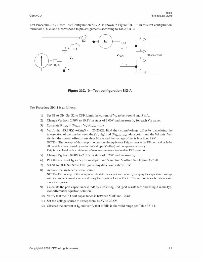
IEEE CSMA/CD Std 802.3af-2003
Test Procedure SIG-1 uses Test Configuration SIG-A as shown in Figure 33C.19. In this test configuration,terminals a, b, c, and d correspond to pin assignments according to Table 33C.2
Test Procedure SIG-1 is as follows:
1) Set S1 to ON. Set S2 to OFF. Limit the current of VN to between 4 and 5 mA.
2) Change VN from 2.70V to 10.1V in steps of 1.00V and measure IN for each VN value.
3) Calculate RsigN = (VN+1 – VN)/(IN+1 – IN).
4) Verify that 23.75KΩ<=RsigN <= 26.25KΩ. Find the current/voltage offset by calculating theintersection of the line between the (VN, IN) and (VN+1, IN+1) data points and the V/I axis. Ver-ify that the current offset is less than 10 µA and the voltage offset is less than 1.9V.NOTE— The concept of this setup is to measure the equivalent Rsig as seen at the PD port and includesall possible errors caused by series diode drops (V offset) and component accuracy.Rsig is calculated with a minimum of two measurements to simulate PSE operation.
5) Change VN from 0.00V to 2.70V in steps of 0.20V and measure IN.
6) Plot the results of IN vs. VN from steps 1 and 5 and find V offset. See Figure 33C.20.
7) Set S1 to OFF. Set S2 to ON. Ignore any data points above 10V.
8) Activate the switched current source.NOTE—The concept of this setup is to calculate the capacitance value by ramping the capacitance voltagewith a constant current source and using the equation I × t = V × C. This method is useful when seriesdiodes are present.
9) Calculate the port capacitance (Cpd) by measuring Rpd (port resistance) and using it in the typ-ical differential equation solution.
10) Verify that the PD port capacitance is between 50nF and 120nF.
11) Set the voltage source to sweep from 14.5V to 20.5V.
12) Observe the current at IN and verify that it falls in the valid range per Table 33–11.
Figure 33C.19—Test configuration SIG-A
a
c
b
d
DD
+
-
IN
S1
PD under TestVN
+
S2
VPort
-I=100µA
Copyright © 2003 IEEE. All rights reserved. 111
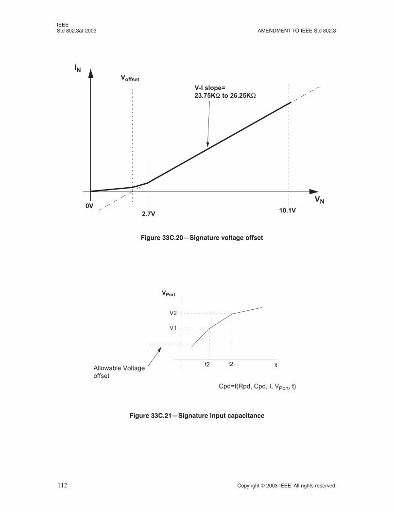
IEEE Std 802.3af-2003 AMENDMENT TO IEEE Std 802.3
Figure 33C.20—Signature voltage offset
IN
VN
2.7V 10.1V0V
Voffset
V-I slope=23.75KΩ to 26.25KΩ
Figure 33C.21—Signature input capacitance
VPort
tAllowable Voltageoffset
V2
V1
Cpd=f(Rpd, Cpd, I, VPort, t)
t2t2
112 Copyright © 2003 IEEE. All rights reserved.
IEEE CSMA/CD Std 802.3af-2003
33C.5 Recommended PD power supply test procedures
33C.5.1 Test Procedure PD-1 (all parameters)
Test Procedure PD-1 is used for testing the following:
a) VOff (Table 33–12, item 8b),b) VOn (Table 33–12, item 8a),c) IPort (max input current during startup) at Vpse=44Vdc (Table 33–12, item 5),d) IPort (max input current during startup) at Vpse=57Vdc (Table 33–12, item 5),e) IPort (max average input current during normal powering mode at VPort=37Vdc) (Table 33–12, item
3),f) PPort (max input power at 37Vdc) (Table 33–12, item 2),g) Max input peak current at VPort=37Vdc and max load (Table 33–12, item 2),h) IPort (max average input current during normal powering mode at VPort=57Vdc) (Table 33–12, item
3),i) PPort (max input power at 57Vdc) (Table 33–12, item 2),j) Max input peak current at VPort=57Vdc and max load (Table 33–12, item 2),k) IPort (min input current at VPort=37Vdc) (Table 33–13, item 1),l) IPort (min input current at VPort=57Vdc) (Table 33–13, item 1),m) Polarity insensitivity when PD implements Auto-MDI-X (33.3.1), and n) PD false underload timing limitations (33.3.6.1).
Test Procedure PD-1 uses Test Configuration PD-A as shown in Figure 33C.22. In this test configuration,terminals a, b, c, and d correspond to pin assignments according to Table 33C.2.CL is a controlled current limit device with two threshold settings, CL1 and CL2.CL1 and CL2 are time-limited to TCL1 and TCL2.If IPort > = CL1 for t > TCL1, then S1 is opened and test is failed.
Copyright © 2003 IEEE. All rights reserved. 113
IEEE Std 802.3af-2003 AMENDMENT TO IEEE Std 802.3
.
Test Procedure PD-1 is as follows:
1) Set S1 to OFF. Set S2 to ON. Set V1 to 30.0V. Set CL1=CL2=1.0A.
2) Set S1 to ON. Wait 1sec and verify that IPort< 1.14mA(=30V/26.25KΩ)
3) Set S1 to OFF. Set S2 to OFF. Set V1 to 44.0V. Set V2=0.0V. SetCL1=CL2=0.4A,TCL1=50ms, CL2=350.0mA and TCL2=5sec. Set PD for max load mode.
4) Set S1 to ON.
5) Record the following parameters: IInrush, TInrush, Von. See Figure 33C.23.
6) Set S1 to OFF.
7) Set V1 to 57.0V. Set S1 to ON and record the following parameters: IInrush, TInrush, Von. SeeFigure 33C.23.
8) Set S2 to ON. Set V1 = 37.0V, V2 = 0.0V, CL1 = 0.4A, TCL1 = 50ms, CL2 = 350.0mA andTCL2=5sec. Set PD for max load mode.
9) Wait 1sec and record Iport_dc and Iport_ac parameters. See Figure 33C.23.
10) Set V1=57V and repeat steps 8,9.
11) Set S2 to ON. Set V1 = 30.0V, V2 = 0.0V, CL1 = 0.4A, TCL1=50ms, CL2=350.0mA andTCL2=5sec. Set PD for max load mode.
12) Increase V1 until PD power supply turns ON. Verify that V1<=Von.
Figure 33C.22—Test configuration PD-A
a
c
b
d
DD
+
IPort
PD under Test
S2
VPort
-
S1
Vsource
+
-
Vpse
20Ω(*)
(*) Models the maxcable resistance
Control
a
c
b
d
+
IPort
PD under TestVPort
-V2
Vpse
20Ω+/-1%
S2
BB
AACurrentLimit
CC
-
+
-
+
S3
V1
0.47µF
PSE test circuit
An example of the test circuit above Vcm
114 Copyright © 2003 IEEE. All rights reserved.
IEEE CSMA/CD Std 802.3af-2003
13) Set S1 to OFF. Set S2 to ON. Set V1 = 37.0V, V2 = 0.0V, CL1 = 0.4A, TCL1=50ms,CL2=350.0mA and TCL2=5sec. Set PD to min load if applicable.
14) Set V1=57.0V. Verify that IPort>= 10mA.
15) If the PD implements Auto-MDI-X, repeat steps 3, 4, and 5, and verify PD operation withreverse polarity connection.
16) Set V1=44V and V2=13V. Set PD to its minimum operating load.
17) Wait 1sec until IPort is stable.
18) Set S3 to OFF and monitor IPort. Verify that IPort is less than 10mA for only TUNLD<290ms.If IPort is not less than 10mA for any time duration, then timing requirement is ignored.See Figure 33C.24.
19) To verify PD input capacitance during normal operating mode:Set S1 to OFF. Set S2 to ON. Set V1=57.0V, V2=0.0V, CL1=CL2=1.0A,TCL1=TCL2=10sec.Set PD for constant load.
20) Set S1 to ON.
21) Wait 1sec and measure IPort.
22) Set S1 to OFF while monitoring VPort. Measure the time duration, Tdrop for VPort to drop from57.0V to 56.0V.Calculate C=IPort ×Tdrop/1V. Verify that 5µF<C<180µF.
23) If C>180µF, set CL1=CL2=1.0A, TCL1=TCL2=5sec.Repeat all tests regarding inrush current limitation and verify that inrush current is limited bythe PD to 0.4A max.
24) Set V1 to 44V, V2=0V. Set S1 to ON. Measure VPort and Vcm noise level at VPort between 37Vand 57V and at all known PD operating conditions.
Iport 0 t 1ms< <( ) 0.025
t-------------=
Figure 33C.23—PD inrush current timing and max peak ripple current and time duration at normal powering mode
IPort
S1 setto ON
1ms
2ms
IINRUSH=5Ap max
IPort(max)=0.4A max
Current limit level
IPort dc max=12.95/VPort
10mA min
TINRUSH=50ms max
ton=50ms max
T>ton/0.05
Peak current limited by PD loaddesign to 0.4A max
t
Copyright © 2003 IEEE. All rights reserved. 115
IEEE Std 802.3af-2003 AMENDMENT TO IEEE Std 802.3
Figure 33C.24—PD underload timing
IPort
VPort
57.0V
44.0V
t
t
S3 setto OFF
tf<1ms
10mA min
TUNLD<290ms
116 Copyright © 2003 IEEE. All rights reserved.
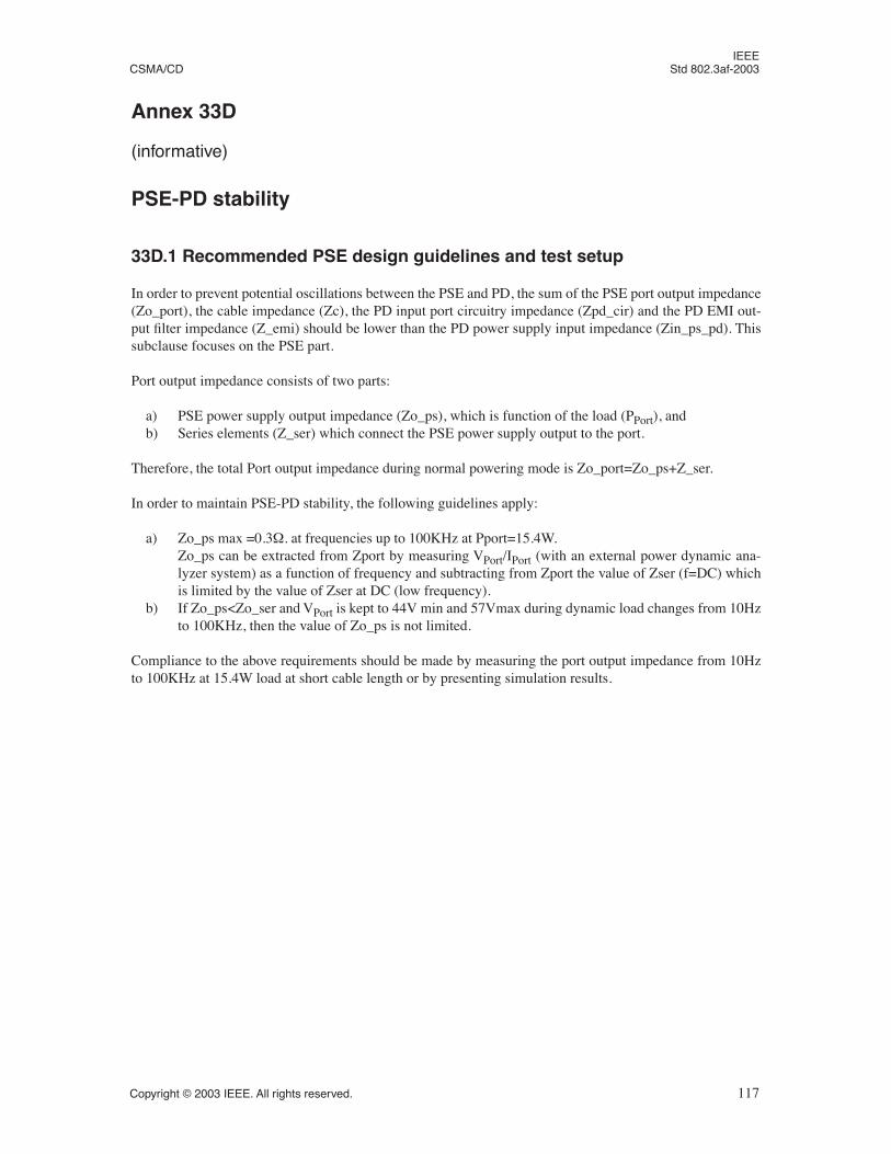
IEEE CSMA/CD Std 802.3af-2003
Annex 33D
(informative)
PSE-PD stability
33D.1 Recommended PSE design guidelines and test setup
In order to prevent potential oscillations between the PSE and PD, the sum of the PSE port output impedance(Zo_port), the cable impedance (Zc), the PD input port circuitry impedance (Zpd_cir) and the PD EMI out-put filter impedance (Z_emi) should be lower than the PD power supply input impedance (Zin_ps_pd). Thissubclause focuses on the PSE part.
Port output impedance consists of two parts:
a) PSE power supply output impedance (Zo_ps), which is function of the load (PPort), andb) Series elements (Z_ser) which connect the PSE power supply output to the port.
Therefore, the total Port output impedance during normal powering mode is Zo_port=Zo_ps+Z_ser.
In order to maintain PSE-PD stability, the following guidelines apply:
a) Zo_ps max =0.3Ω. at frequencies up to 100KHz at Pport=15.4W.Zo_ps can be extracted from Zport by measuring VPort/IPort (with an external power dynamic ana-lyzer system) as a function of frequency and subtracting from Zport the value of Zser (f=DC) whichis limited by the value of Zser at DC (low frequency).
b) If Zo_ps<Zo_ser and VPort is kept to 44V min and 57Vmax during dynamic load changes from 10Hzto 100KHz, then the value of Zo_ps is not limited.
Compliance to the above requirements should be made by measuring the port output impedance from 10Hzto 100KHz at 15.4W load at short cable length or by presenting simulation results.
Copyright © 2003 IEEE. All rights reserved. 117
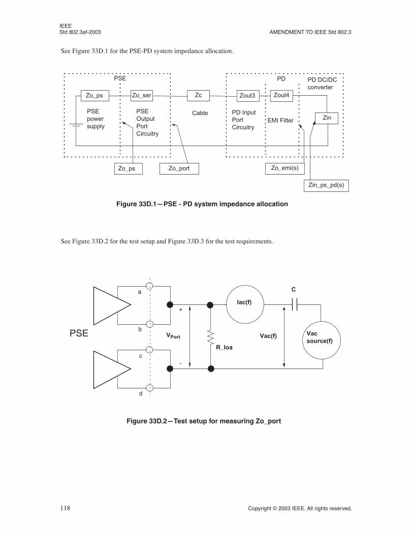
IEEE Std 802.3af-2003 AMENDMENT TO IEEE Std 802.3
See Figure 33D.1 for the PSE-PD system impedance allocation.
See Figure 33D.2 for the test setup and Figure 33D.3 for the test requirements.
Figure 33D.1—PSE - PD system impedance allocation
Zo_ps
Zo_ps
Zo_ser
Zo_port
Zc Zout3 Zout4
Zin
Zo_emi(s)
Zin_ps_pd(s)
PSEpowersupply
PSE PD
PSEOutputPortCircuitry
Cable PD InputPortCircuitry
EMI Filter
PD DC/DCconverter
Figure 33D.2—Test setup for measuring Zo_port
a
c
b
d
+
-
VPort
Iac(f)
PSE Vacsource(f)
C
Vac(f)
R_loa
118 Copyright © 2003 IEEE. All rights reserved.
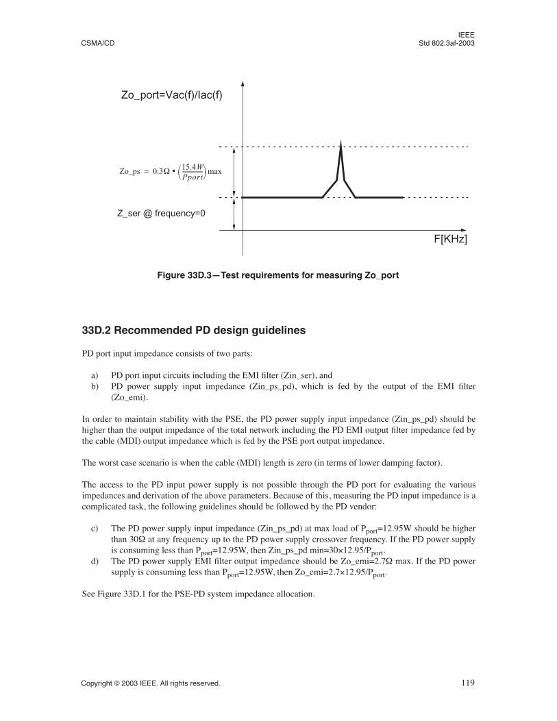
IEEE CSMA/CD Std 802.3af-2003
33D.2 Recommended PD design guidelines
PD port input impedance consists of two parts:
a) PD port input circuits including the EMI filter (Zin_ser), andb) PD power supply input impedance (Zin_ps_pd), which is fed by the output of the EMI filter
(Zo_emi).
In order to maintain stability with the PSE, the PD power supply input impedance (Zin_ps_pd) should behigher than the output impedance of the total network including the PD EMI output filter impedance fed bythe cable (MDI) output impedance which is fed by the PSE port output impedance.
The worst case scenario is when the cable (MDI) length is zero (in terms of lower damping factor).
The access to the PD input power supply is not possible through the PD port for evaluating the variousimpedances and derivation of the above parameters. Because of this, measuring the PD input impedance is acomplicated task, the following guidelines should be followed by the PD vendor:
c) The PD power supply input impedance (Zin_ps_pd) at max load of Pport=12.95W should be higherthan 30Ω at any frequency up to the PD power supply crossover frequency. If the PD power supplyis consuming less than Pport=12.95W, then Zin_ps_pd min=30×12.95/Pport.
d) The PD power supply EMI filter output impedance should be Zo_emi=2.7Ω max. If the PD powersupply is consuming less than Pport=12.95W, then Zo_emi=2.7×12.95/Pport.
See Figure 33D.1 for the PSE-PD system impedance allocation.
Figure 33D.3—Test requirements for measuring Zo_port
Zo_port=Vac(f)/Iac(f)
F[KHz]
Z_ser @ frequency=0
Zo_ps 0.3Ω 15.4WPport---------------
• max=
Copyright © 2003 IEEE. All rights reserved. 119
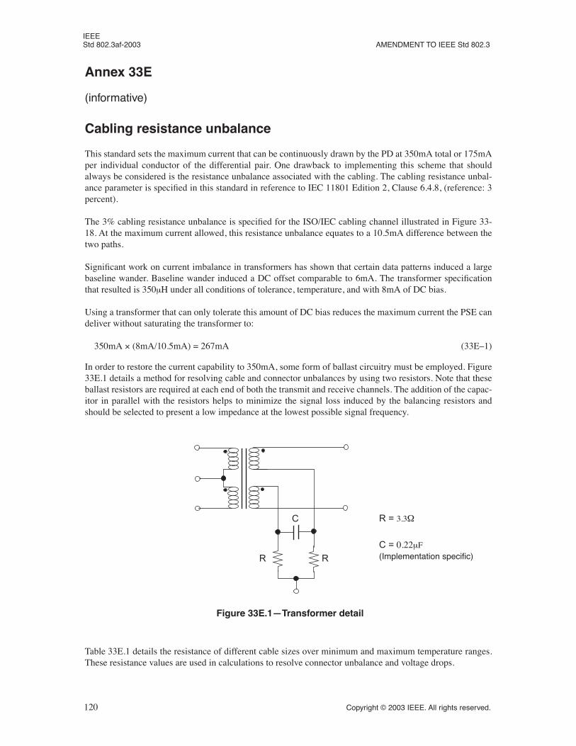
IEEE Std 802.3af-2003 AMENDMENT TO IEEE Std 802.3
Annex 33E
(informative)
Cabling resistance unbalance
This standard sets the maximum current that can be continuously drawn by the PD at 350mA total or 175mAper individual conductor of the differential pair. One drawback to implementing this scheme that shouldalways be considered is the resistance unbalance associated with the cabling. The cabling resistance unbal-ance parameter is specified in this standard in reference to IEC 11801 Edition 2, Clause 6.4.8, (reference: 3percent).
The 3% cabling resistance unbalance is specified for the ISO/IEC cabling channel illustrated in Figure 33-18. At the maximum current allowed, this resistance unbalance equates to a 10.5mA difference between thetwo paths.
Significant work on current imbalance in transformers has shown that certain data patterns induced a largebaseline wander. Baseline wander induced a DC offset comparable to 6mA. The transformer specificationthat resulted is 350µH under all conditions of tolerance, temperature, and with 8mA of DC bias.
Using a transformer that can only tolerate this amount of DC bias reduces the maximum current the PSE candeliver without saturating the transformer to:
350mA × (8mA/10.5mA) = 267mA (33E–1)
In order to restore the current capability to 350mA, some form of ballast circuitry must be employed. Figure33E.1 details a method for resolving cable and connector unbalances by using two resistors. Note that theseballast resistors are required at each end of both the transmit and receive channels. The addition of the capac-itor in parallel with the resistors helps to minimize the signal loss induced by the balancing resistors andshould be selected to present a low impedance at the lowest possible signal frequency.
Table 33E.1 details the resistance of different cable sizes over minimum and maximum temperature ranges.These resistance values are used in calculations to resolve connector unbalance and voltage drops.
Figure 33E.1—Transformer detail
R = 3.3Ω
C = 0.22µF(Implementation specific)R R
C
120 Copyright © 2003 IEEE. All rights reserved.
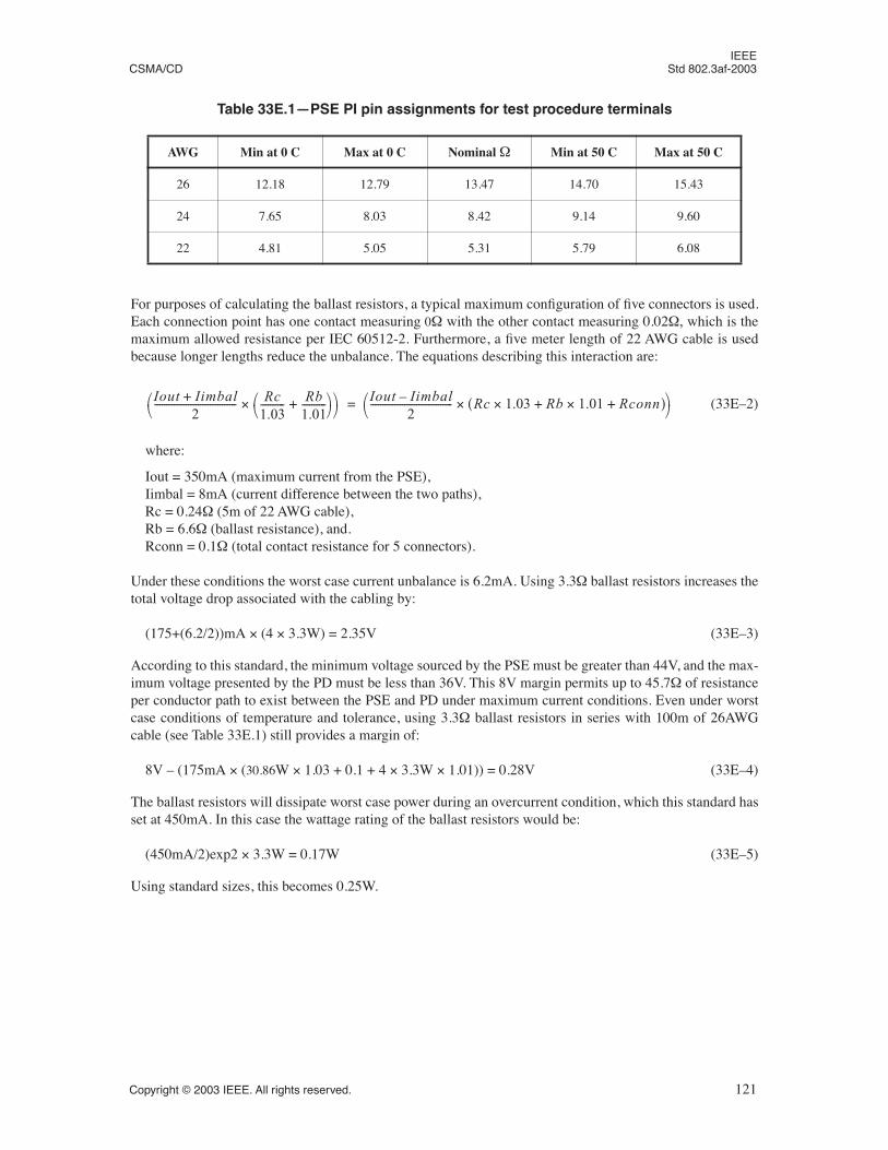
IEEE
CSMA/CD Std 802.3af-2003
For purposes of calculating the ballast resistors, a typical maximum configuration of five connectors is used.Each connection point has one contact measuring 0Ω with the other contact measuring 0.02Ω, which is themaximum allowed resistance per IEC 60512-2. Furthermore, a five meter length of 22 AWG cable is usedbecause longer lengths reduce the unbalance. The equations describing this interaction are:
(33E–2)
where:
Iout = 350mA (maximum current from the PSE),Iimbal = 8mA (current difference between the two paths),Rc = 0.24Ω (5m of 22 AWG cable),Rb = 6.6Ω (ballast resistance), and.Rconn = 0.1Ω (total contact resistance for 5 connectors).
Under these conditions the worst case current unbalance is 6.2mA. Using 3.3Ω ballast resistors increases thetotal voltage drop associated with the cabling by:
(175+(6.2/2))mA × (4 × 3.3W) = 2.35V (33E–3)
According to this standard, the minimum voltage sourced by the PSE must be greater than 44V, and the max-imum voltage presented by the PD must be less than 36V. This 8V margin permits up to 45.7Ω of resistanceper conductor path to exist between the PSE and PD under maximum current conditions. Even under worstcase conditions of temperature and tolerance, using 3.3Ω ballast resistors in series with 100m of 26AWGcable (see Table 33E.1) still provides a margin of:
8V – (175mA × (30.86W × 1.03 + 0.1 + 4 × 3.3W × 1.01)) = 0.28V (33E–4)
The ballast resistors will dissipate worst case power during an overcurrent condition, which this standard hasset at 450mA. In this case the wattage rating of the ballast resistors would be:
(450mA/2)exp2 × 3.3W = 0.17W (33E–5)
Using standard sizes, this becomes 0.25W.
Table 33E.1—PSE PI pin assignments for test procedure terminals
AWG Min at 0 C Max at 0 C Nominal Ω Min at 50 C Max at 50 C
26 12.18 12.79 13.47 14.70 15.43
24 7.65 8.03 8.42 9.14 9.60
22 4.81 5.05 5.31 5.79 6.08
Iout Iimbal+2
---------------------------------- Rc1.03---------- Rb
1.01----------+
× Iout Iimbal–
2---------------------------------- Rc 1.03 Rb+× 1.01 Rconn+×( )×
=
Copyright © 2003 IEEE. All rights reserved. 121