Embed Size (px)
Citation preview
Single-Port, 40W, IEEE 802.3af/at, PSE Controller with I2C
MAX5971B
EVALUATION KIT AVAILABLE
19-5336; Rev 3; 3/16
General DescriptionThe MAX5971B is a single-port power controller designed for use in IEEEM 802.3af/at-compliant power-sourcing equipment (PSE). This device provides powered device (PD) discovery, classification, current limit, and DC and AC load-disconnect detections. The MAX5971B supports both fully automatic operation and software program-mability, and features an integrated power MOSFET and sense resistor. The device supports detection and classification operation from a single 54V supply. In addi-tion, it supports 2-event classification and new Class 5 classification of high-power PDs. The MAX5971B pro-vides up to 40W to a single port (Class 5 enabled) and still provides high-capacitance detection for legacy PDs.
The device provides four operating modes to suit different system requirements. By default, auto mode allows the device to operate automatically at its default settings without any software. Semiautomatic mode automatically detects and classifies a device connected to the port after initial software activation, but does not power the port until instructed to by software. Manual mode allows total software control of the device and is useful for system diagnostics. Shutdown mode terminates all port activities and securely turns off power to the port.
The IC features an I2C-compatible, 2-wire serial interface, and is fully software-configurable and programmable. The device provides instantaneous readout of port cur-rent through the I2C interface. The device’s extensive programmability enhances system flexibility, enables field diagnosis and allows for uses in other, non standard applications.
The device provides input undervoltage lockout (UVLO), input undervoltage detection, input overvoltage lockout, overtemperature protection, output voltage slew-rate limit during startup, and LED status indication. The MAX5971B programmability includes startup timeout, overcurrent timeout, and load-disconnect detection timeout.
The device is available in a space-saving, 28-pin TQFN (5mm x 5mm) power package and is rated for the extended (-40NC to +105NC) temperature range.
ApplicationsSingle-Port PSE End-Point Applications
Single-Port PSE Power Injectors (Midspan Applications)
Switches/Routers
FeaturesS IEEE 802.3af/at CompliantS Up to 40W for Single-Port PSE ApplicationsS Integrated Power MOSFET and Sense ResistorS Supports 54V Single-Supply OperationS PD Detection and ClassificationS I2C-Compatible, 2-Wire Serial InterfaceS Instantaneous Readout of Port Current Through
I2C InterfaceS Programmable Current Limit for Class 5 PDsS High-Capacitance Detection for Legacy DevicesS Supports Both DC and AC Load Removal
DetectionsS Current Foldback and Duty-Cycle-Controlled
Current LimitS LED Indicator for Port StatusS Direct Fast-Shutdown Control CapabilityS Space-Saving, 28-Pin TQFN (5mm x 5mm) Power
Package
Ordering Information
IEEE is a registered service mark of the Institute of Electrical and Electronics Engineers, Inc.
Typical Operating Circuit
+Denotes a lead(Pb)-free/RoHS-compliant package.*EP = Exposed pad.
-54V AGND
SDA SCL AD0 INT
LED
PWMEN
VEE_DIG
VEE
LEGACY
MIDSPAN
OSC
EN
OUT
OUTP
DET
ILIM1
ILIM2
MAX5971B
PSE OUTPUT
SERIAL INTERFACE
PART TEMP RANGE PIN-PACKAGE
MAX5971BETI+ -40NC to +105NC 28 TQFN-EP*
For pricing, delivery, and ordering information, please contact Maxim Direct at 1-888-629-4642, or visit Maxim’s website at www.maximintegrated.com.
2 Maxim Integrated
Single-Port, 40W, IEEE 802.3af/at, PSE Controller with I2C
MAX5971B
Stresses beyond those listed under “Absolute Maximum Ratings” may cause permanent damage to the device. These are stress ratings only, and functional operation of the device at these or any other conditions beyond those indicated in the operational sections of the specifications is not implied. Exposure to absolute maximum rating conditions for extended periods may affect device reliability.
ELECTRICAL CHARACTERISTICS(VAGND - VEE = 32V to 60V, TA = -40NC to +105NC, all voltages are referenced to VEE, unless otherwise noted. Typical values are at VAGND - VEE = +54V, TA = +25NC. Currents are positive when entering the pin and negative otherwise.) (Note 2)
ABSOLUTE MAXIMUM RATINGS(Voltages referenced to VEE, unless otherwise noted.)AGND, DET, LED ..................................................-0.3V to +80VOUT ...................................................... -0.3V to (VAGND + 0.3V)OUTP ....................................................... -6V to (VAGND + 0.3V)VEE_DIG ................................................................-0.3V to +0.3VOSC .........................................................................-0.3V to +6VEN, PWMEN, MIDSPAN, LEGACY, ILIM1, ILIM2 ....-0.3V to +4VINT, AD0, SCL, SDA ................................................-0.3V to +6VMaximum Current into INT and SDA ..................................80mA
Maximum Current into LED ................................................40mAMaximum Current into OUT ........................Internally RegulatedContinuous Power Dissipation (TA = +70NC) 28-Pin TQFN (derate 34.5mW/NC above +70NC) ......2758mWOperating Temperature Range ........................ -40NC to +105NCStorage Temperature Range ............................ -65NC to +150NCJunction Temperature .....................................................+150NCLead Temperature (soldering, 10s) ................................+300NCSoldering Temperature (reflow) ......................................+260NC
28 TQFN Junction-to-Ambient Thermal Resistance (qJA) ..........29°C/W
Junction-to-Case Thermal Resistance (qJC) .................2°C/W
Note 1: Package thermal resistances were obtained using the method described in JEDEC specification JESD51-7, using a four-lay-er board. For detailed information on package thermal considerations, refer to www.maximintegrated.com/thermal-tutorial.
PACKAGE THERMAL CHARACTERISTICS (Note 1)
PARAMETER SYMBOL CONDITIONS MIN TYP MAX UNITS
POWER SUPPLIES
Operating Voltage Range VAGND VAGND - VEE 32 60 V
Supply Current IEEVOUT = VEE, all logic inputs unconnected, measured at AGND in power mode
2.5 4 mA
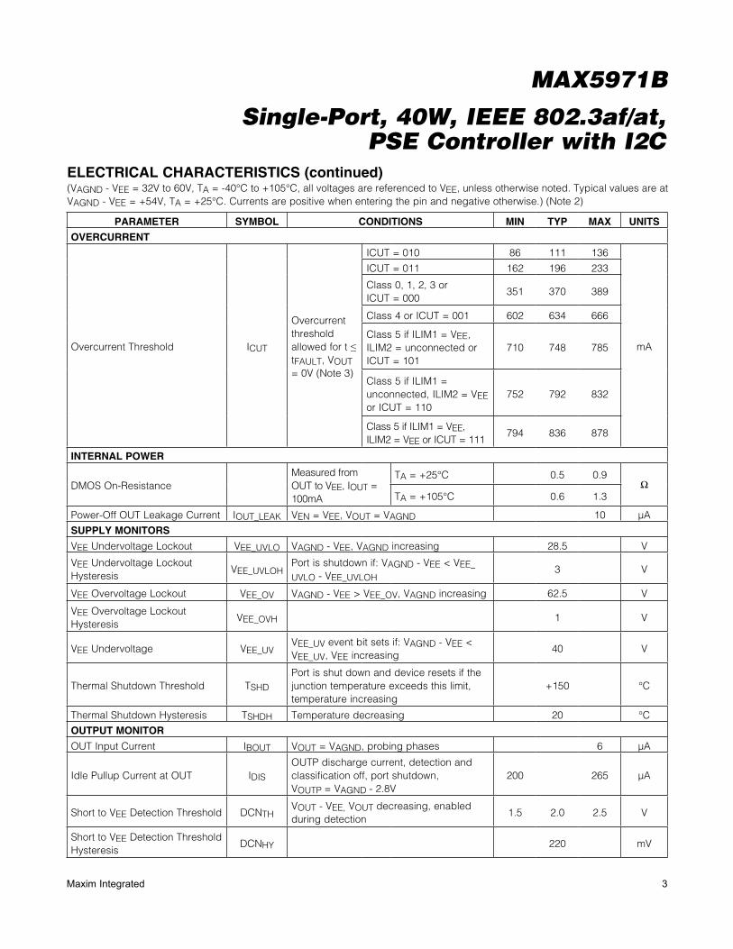
CURRENT LIMIT
Current Limit ILIM
Maximum ILOAD allowed during current-limit conditions, VOUT = 0V (Note 3)
ICUT = 010 98 126 155
mA
ICUT = 011 185 223 265
Class 0, 1, 2, 3 or ICUT = 000
400 420 441
Class 4 or ICUT = 001 684 720 756
Class 5 if ILIM1 = VEE, ILIM2 = unconnected or ICUT = 101
807 850 893
Class 5 if ILIM1 = unconnected, ILIM2 = VEE or ICUT = 110
855 900 945
Class 5 if ILIM1 = VEE, ILIM2 = VEE or ICUT = 111
902 950 998
Foldback Initial OUT Voltage VFLBK_STVAGND - VOUT below which the current limit starts folding back
27 V
Foldback Final OUT Voltage VFLBK_ENDVAGND - VOUT below which the current limit reaches ITH_FB
10 V
Minimum Foldback Current-Limit Threshold
ITH_FB VOUT = VAGND 166 mA
3Maxim Integrated
Single-Port, 40W, IEEE 802.3af/at, PSE Controller with I2C
MAX5971B
ELECTRICAL CHARACTERISTICS (continued)(VAGND - VEE = 32V to 60V, TA = -40NC to +105NC, all voltages are referenced to VEE, unless otherwise noted. Typical values are at VAGND - VEE = +54V, TA = +25NC. Currents are positive when entering the pin and negative otherwise.) (Note 2)
PARAMETER SYMBOL CONDITIONS MIN TYP MAX UNITS
OVERCURRENT
Overcurrent Threshold ICUT
Overcurrent threshold allowed for t P tFAULT, VOUT = 0V (Note 3)
ICUT = 010 86 111 136
mA
ICUT = 011 162 196 233
Class 0, 1, 2, 3 or ICUT = 000
351 370 389
Class 4 or ICUT = 001 602 634 666
Class 5 if ILIM1 = VEE, ILIM2 = unconnected or ICUT = 101
710 748 785
Class 5 if ILIM1 = unconnected, ILIM2 = VEE or ICUT = 110
752 792 832
Class 5 if ILIM1 = VEE, ILIM2 = VEE or ICUT = 111
794 836 878
INTERNAL POWER
DMOS On-ResistanceMeasured from OUT to VEE, IOUT = 100mA
TA = +25NC 0.5 0.9I
TA = +105NC 0.6 1.3
Power-Off OUT Leakage Current IOUT_LEAK VEN = VEE, VOUT = VAGND 10 FA
SUPPLY MONITORS
VEE Undervoltage Lockout VEE_UVLO VAGND - VEE, VAGND increasing 28.5 V
VEE Undervoltage Lockout Hysteresis
VEE_UVLOHPort is shutdown if: VAGND - VEE < VEE_UVLO - VEE_UVLOH
3 V
VEE Overvoltage Lockout VEE_OV VAGND - VEE > VEE_OV, VAGND increasing 62.5 V
VEE Overvoltage Lockout Hysteresis
VEE_OVH 1 V
VEE Undervoltage VEE_UVVEE_UV event bit sets if: VAGND - VEE < VEE_UV, VEE increasing
40 V
Thermal Shutdown Threshold TSHD
Port is shut down and device resets if the junction temperature exceeds this limit, temperature increasing
+150 NC
Thermal Shutdown Hysteresis TSHDH Temperature decreasing 20 NC
OUTPUT MONITOR
OUT Input Current IBOUT VOUT = VAGND, probing phases 6 FA
Idle Pullup Current at OUT IDIS
OUTP discharge current, detection and classification off, port shutdown,VOUTP = VAGND - 2.8V
200 265 FA
Short to VEE Detection Threshold DCNTHVOUT - VEE, VOUT decreasing, enabled during detection
1.5 2.0 2.5 V
Short to VEE Detection Threshold Hysteresis
DCNHY 220 mV
4 Maxim Integrated
Single-Port, 40W, IEEE 802.3af/at, PSE Controller with I2C
MAX5971B
ELECTRICAL CHARACTERISTICS (continued)(VAGND - VEE = 32V to 60V, TA = -40NC to +105NC, all voltages are referenced to VEE, unless otherwise noted. Typical values are at VAGND - VEE = +54V, TA = +25NC. Currents are positive when entering the pin and negative otherwise.) (Note 2)
PARAMETER SYMBOL CONDITIONS MIN TYP MAX UNITS
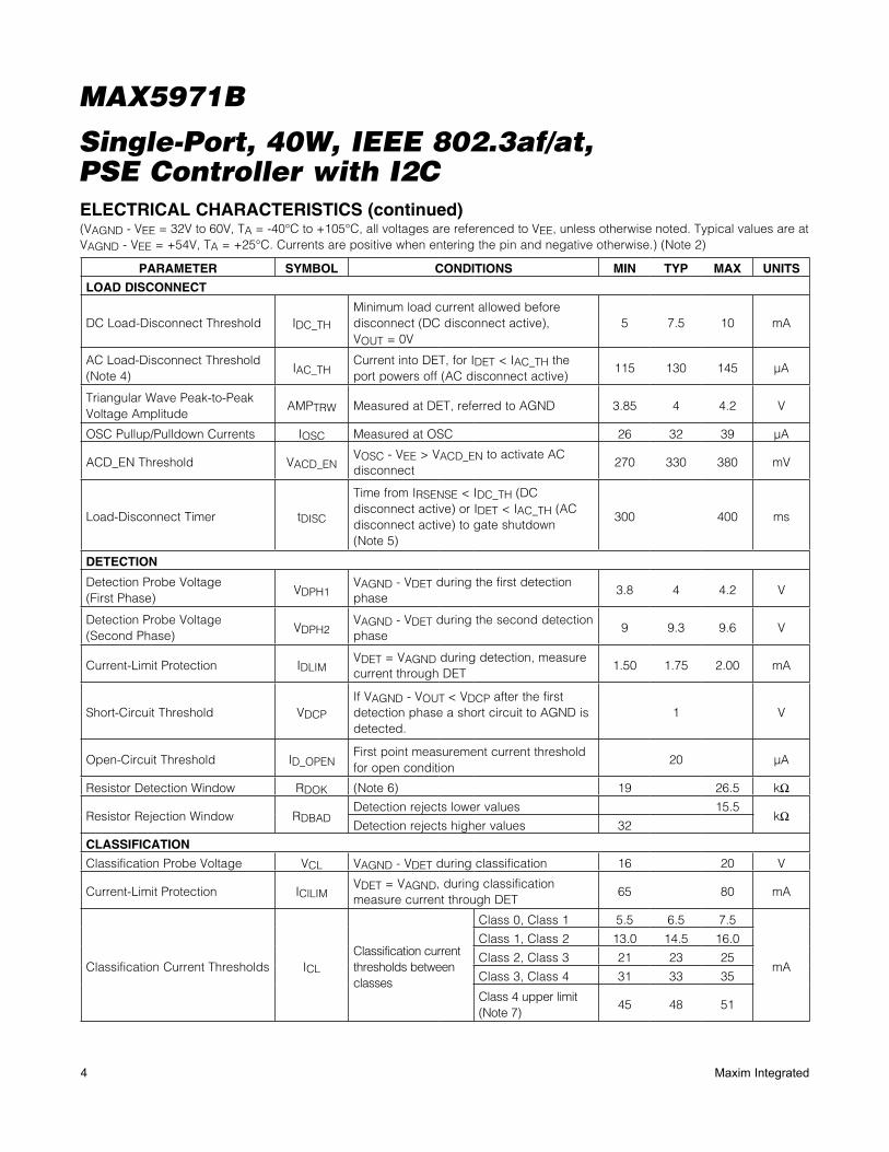
LOAD DISCONNECT
DC Load-Disconnect Threshold IDC_TH
Minimum load current allowed before disconnect (DC disconnect active), VOUT = 0V
5 7.5 10 mA
AC Load-Disconnect Threshold (Note 4)
IAC_THCurrent into DET, for IDET < IAC_TH the port powers off (AC disconnect active)
115 130 145 FA
Triangular Wave Peak-to-Peak Voltage Amplitude
AMPTRW Measured at DET, referred to AGND 3.85 4 4.2 V
OSC Pullup/Pulldown Currents IOSC Measured at OSC 26 32 39 FA
ACD_EN Threshold VACD_ENVOSC - VEE > VACD_EN to activate AC disconnect
270 330 380 mV
Load-Disconnect Timer tDISC
Time from IRSENSE < IDC_TH (DC disconnect active) or IDET < IAC_TH (AC disconnect active) to gate shutdown (Note 5)
300 400 ms
DETECTION
Detection Probe Voltage (First Phase)
VDPH1VAGND - VDET during the first detection phase
3.8 4 4.2 V
Detection Probe Voltage (Second Phase)
VDPH2VAGND - VDET during the second detection phase
9 9.3 9.6 V
Current-Limit Protection IDLIMVDET = VAGND during detection, measure current through DET
1.50 1.75 2.00 mA
Short-Circuit Threshold VDCP
If VAGND - VOUT < VDCP after the first detection phase a short circuit to AGND is detected.
1 V
Open-Circuit Threshold ID_OPENFirst point measurement current threshold for open condition
20 FA
Resistor Detection Window RDOK (Note 6) 19 26.5 kI
Resistor Rejection Window RDBADDetection rejects lower values 15.5
kIDetection rejects higher values 32
CLASSIFICATION
Classification Probe Voltage VCL VAGND - VDET during classification 16 20 V
Current-Limit Protection IClLIMVDET = VAGND, during classification measure current through DET
65 80 mA
Classification Current Thresholds ICL
Classification current thresholds between classes
Class 0, Class 1 5.5 6.5 7.5
mA
Class 1, Class 2 13.0 14.5 16.0
Class 2, Class 3 21 23 25
Class 3, Class 4 31 33 35
Class 4 upper limit (Note 7)
45 48 51
5Maxim Integrated
Single-Port, 40W, IEEE 802.3af/at, PSE Controller with I2C
MAX5971B
ELECTRICAL CHARACTERISTICS (continued)(VAGND - VEE = 32V to 60V, TA = -40NC to +105NC, all voltages are referenced to VEE, unless otherwise noted. Typical values are at VAGND - VEE = +54V, TA = +25NC. Currents are positive when entering the pin and negative otherwise.) (Note 2)
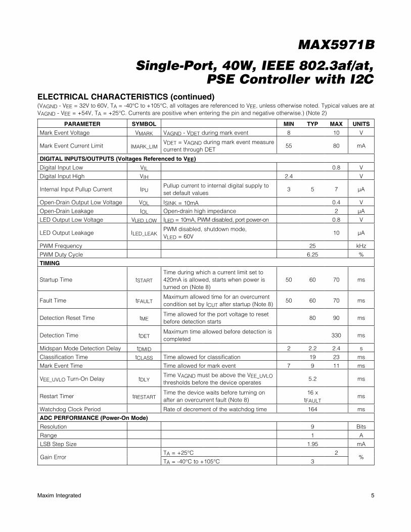
PARAMETER SYMBOL MIN TYP MAX UNITS
Mark Event Voltage VMARK VAGND - VDET during mark event 8 10 V
Mark Event Current Limit IMARK_LIMVDET = VAGND during mark event measure current through DET
55 80 mA
DIGITAL INPUTS/OUTPUTS (Voltages Referenced to VEE)
Digital Input Low VIL 0.8 V
Digital Input High VIH 2.4 V
Internal Input Pullup Current IPUPullup current to internal digital supply to set default values
3 5 7 FA
Open-Drain Output Low Voltage VOL ISINK = 10mA 0.4 V
Open-Drain Leakage IOL Open-drain high impedance 2 FA
LED Output Low Voltage VLED_LOW ILED = 10mA, PWM disabled, port power-on 0.8 V
LED Output Leakage ILED_LEAKPWM disabled, shutdown mode, VLED = 60V
10 FA
PWM Frequency 25 kHz
PWM Duty Cycle 6.25 %
TIMING
Startup Time tSTART
Time during which a current limit set to 420mA is allowed, starts when power is turned on (Note 8)
50 60 70 ms
Fault Time tFAULTMaximum allowed time for an overcurrent condition set by ICUT after startup (Note 8)
50 60 70 ms
Detection Reset Time tMETime allowed for the port voltage to reset before detection starts
80 90 ms
Detection Time tDETMaximum time allowed before detection is completed
330 ms
Midspan Mode Detection Delay tDMID 2 2.2 2.4 s
Classification Time tCLASS Time allowed for classification 19 23 ms
Mark Event Time Time allowed for mark event 7 9 11 ms
VEE_UVLO Turn-On Delay tDLYTime VAGND must be above the VEE_UVLO thresholds before the device operates
5.2 ms
Restart Timer tRESTARTTime the device waits before turning on after an overcurrent fault (Note 8)
16 x tFAULT
ms
Watchdog Clock Period Rate of decrement of the watchdog time 164 ms
ADC PERFORMANCE (Power-On Mode)
Resolution 9 Bits
Range 1 A
LSB Step Size 1.95 mA
Gain ErrorTA = +25NC 2
%TA = -40NC to +105NC 3
6 Maxim Integrated
Single-Port, 40W, IEEE 802.3af/at, PSE Controller with I2C
MAX5971B
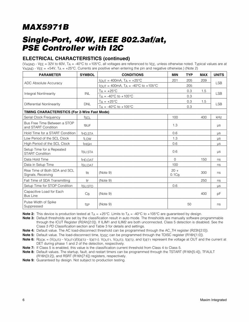
Note 2: This device is production tested at TA = +25°C. Limits to TA = -40°C to +105°C are guaranteed by design.Note 3: Default thresholds are set by the classification result in auto mode. The thresholds are manually software programmable
through the ICUT Register (R2Ah[2:0]). If ILIM1 and ILIM2 are both unconnected, Class 5 detection is disabled. See the Class 5 PD Classification section and Table 3 for details and settings.
Note 4: Default value. The AC load-disconnect threshold can be programmed through the AC_TH register (R23h[2:0]).Note 5: Default value. The load-disconnect time, tDISC can be programmed through the TDISC register (R16h[1:0]).Note 6: RDOK = (VOUT2 - VOUT1)/(IDET2 - IDET1). VOUT1, VOUT2, IDET2, and IDET1 represent the voltage at OUT and the current at
DET during phase 1 and 2 of the detection, respectively.Note 7: If Class 5 is enabled, this value is the classification current threshold from Class 4 to Class 5.Note 8: Default values. The startup, fault, and restart timers can be programmed through the TSTART (R16h[5:4]), TFAULT
(R16h[3:2]), and RSRT (R16h[7:6]) registers, respectively.Note 9: Guaranteed by design. Not subject to production testing.
ELECTRICAL CHARACTERISTICS (continued)(VAGND - VEE = 32V to 60V, TA = -40NC to +105NC, all voltages are referenced to VEE, unless otherwise noted. Typical values are at VAGND - VEE = +54V, TA = +25NC. Currents are positive when entering the pin and negative otherwise.) (Note 2)
PARAMETER SYMBOL CONDITIONS MIN TYP MAX UNITS
ADC Absolute AccuracyIOUT = 400mA, TA = +25NC 201 205 209
LSBIOUT = 400mA, TA = -40NC to +105NC 205
Integral Nonlinearity INLTA = +25NC 0.3 1.5
LSBTA = -40NC to +105NC 0.3
Differential Nonlinearity DNLTA = +25NC 0.3 1.5
LSBTA = -40NC to +105NC 0.3
TIMING CHARACTERISTICS (For 2-Wire Fast Mode)
Serial Clock Frequency fSCL 100 400 kHz
Bus Free Time Between a STOP and START Condition
tBUF 1.3 µs
Hold Time for a START Condition tHD,STA 0.6 µs
Low Period of the SCL Clock tLOW 1.3 µs
High Period of the SCL Clock tHIGH 0.6 µs
Setup Time for a Repeated START Condition
tSU,STA 0.6 µs
Data Hold Time tHD,DAT 0 150 ns
Data in Setup Time tSU,DAT 100 ns
Rise Time of Both SDA and SCL Signals, Receiving
tR (Note 9)20 +
0.1CB300 ns
Fall Time of SDA Transmitting tF (Note 9) 250 ns
Setup Time for STOP Condition tSU,STO 0.6 µs
Capacitive Load for EachBus Line
CB (Note 9) 400 pF
Pulse Width of Spike Suppressed
tSP (Note 9) 50 ns
7Maxim Integrated
Single-Port, 40W, IEEE 802.3af/at, PSE Controller with I2C
MAX5971B
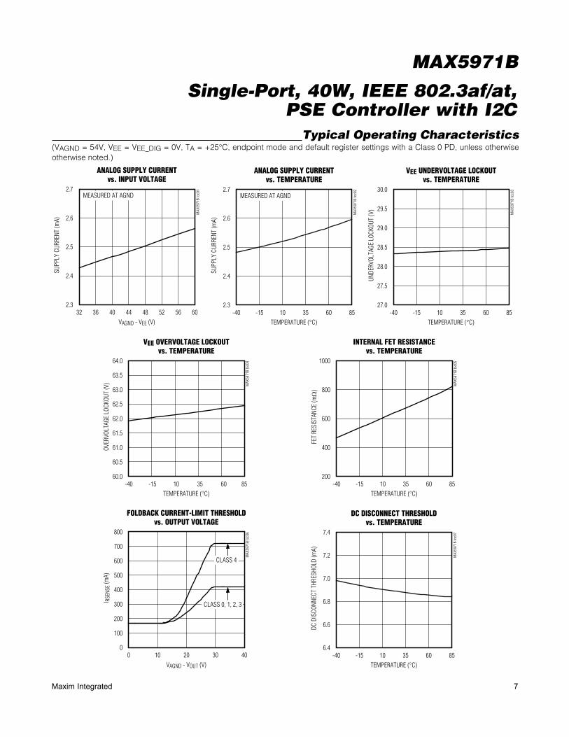
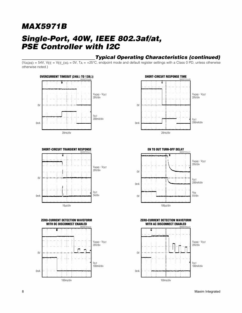
Typical Operating Characteristics(VAGND = 54V, VEE = VEE_DIG = 0V, TA = +25NC, endpoint mode and default register settings with a Class 0 PD, unless otherwise otherwise noted.)
DC DISCONNECT THRESHOLDvs. TEMPERATURE
MAX
5971
B to
c07
TEMPERATURE (°C)
DC D
ISCO
NNEC
T TH
RESH
OLD
(mA)
603510-15
6.6
6.8
7.0
7.2
7.4
6.4-40 85
FOLDBACK CURRENT-LIMIT THRESHOLDvs. OUTPUT VOLTAGE
MAX
5971
B to
c06
VAGND - VOUT (V)
I RSE
NSE
(mA)
302010
100
200
300
400
500
600
700
800
00 40
CLASS 4
CLASS 0, 1, 2, 3
INTERNAL FET RESISTANCEvs. TEMPERATURE
MAX
5971
B to
c05
TEMPERATURE (°C)
FET
RESI
STAN
CE (m
Ω)
603510-15
400
600
800
1000
200-40 85
VEE OVERVOLTAGE LOCKOUTvs. TEMPERATURE
MAX
5971
B to
c04
TEMPERATURE (°C)
OVER
VOLT
AGE
LOCK
OUT
(V)
6035-15 10
60.5
61.0
61.5
62.0
63.0
62.5
63.5
64.0
60.0-40 85
VEE UNDERVOLTAGE LOCKOUTvs. TEMPERATURE
MAX
5971
B to
c03
TEMPERATURE (°C)
UNDE
RVOL
TAGE
LOC
KOUT
(V)
603510-15
27.5
28.0
28.5
29.0
29.5
30.0
27.0-40 85
ANALOG SUPPLY CURRENTvs. TEMPERATURE
MAX
5971
B to
c02
TEMPERATURE (°C)
SUPP
LY C
URRE
NT (m
A)
603510-15
2.4
2.5
2.6
2.7
2.3-40 85
MEASURED AT AGND
ANALOG SUPPLY CURRENTvs. INPUT VOLTAGE
MAX
5971
B to
c01
VAGND - VEE (V)
SUPP
LY C
URRE
NT (m
A)
565248444036
2.4
2.5
2.6
2.7
2.332 60
MEASURED AT AGND
8 Maxim Integrated
Single-Port, 40W, IEEE 802.3af/at, PSE Controller with I2C
MAX5971B
Typical Operating Characteristics (continued)(VAGND = 54V, VEE = VEE_DIG = 0V, TA = +25NC, endpoint mode and default register settings with a Class 0 PD, unless otherwise otherwise noted.)
ZERO-CURRENT DETECTION WAVEFORMWITH AC DISCONNECT ENABLED
MAX5971B toc13
100ms/div
0V
0mA
VAGND - VOUT20V/div
IOUT100mA/div
ZERO-CURRENT DETECTION WAVEFORMWITH DC DISCONNECT ENABLED
MAX5971B toc12
100ms/div
0V
0mA
VAGND - VOUT20V/div
IOUT100mA/div
EN TO OUT TURN-OFF DELAYMAX5971B toc11
100µs/div
0V
0V
0mA
VAGND - VOUT20V/div
IOUT200mA/div
VEN5V/div
SHORT-CIRCUIT TRANSIENT RESPONSEMAX5971B toc10
10µs/div
0V
0mA
VAGND - VOUT20V/div
IOUT5A/div
SHORT-CIRCUIT RESPONSE TIMEMAX5971B toc09
20ms/div
0V
0mA
VAGND - VOUT20V/div
IOUT200mA/div
OVERCURRENT TIMEOUT (240Ω TO 138Ω)MAX5971B toc08
20ms/div
0V
0mA
VAGND - VOUT20V/div
IOUT200mA/div

9Maxim Integrated
Single-Port, 40W, IEEE 802.3af/at, PSE Controller with I2C
MAX5971B
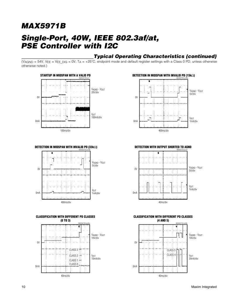
Typical Operating Characteristics (continued)(VAGND = 54V, VEE = VEE_DIG = 0V, TA = +25NC, endpoint mode and default register settings with a Class 0 PD, unless otherwise otherwise noted.)
DETECTION WITH INVALID PD (OPEN CIRCUIT)MAX5971B toc16d
100ms/div
0V
0mA
VAGND - VOUT5V/div
IOUT1mA/div
DETECTION WITH INVALID PD (33kΩ)MAX5971B toc16c
100ms/div
0V
0mA
VAGND - VOUT5V/div
IOUT1mA/div
DETECTION WITH INVALID PD (15kΩ)MAX5971B toc16b
100ms/div
0V
0mA
VAGND - VOUT5V/div
IOUT1mA/div
DETECTION WITH INVALID PD (25kΩ AND 10µF)MAX5971B toc16a
40ms/div
0V
0mA
VAGND - VOUT1V/div
IOUT1mA/div
STARTUP WITH A VALID PDMAX5971B toc15
100ms/div
0V
0mA
VAGND - VOUT20V/div
IOUT100mA/div
OVERCURRENT RESTART DELAYMAX5971B toc14
400ms/div
0V
0mA
VAGND - VOUT20V/div
IOUT200mA/div
10 Maxim Integrated
Single-Port, 40W, IEEE 802.3af/at, PSE Controller with I2C
MAX5971B
Typical Operating Characteristics (continued)(VAGND = 54V, VEE = VEE_DIG = 0V, TA = +25NC, endpoint mode and default register settings with a Class 0 PD, unless otherwise otherwise noted.)
CLASSIFICATION WITH DIFFERENT PD CLASSES(4 AND 5)
MAX5971B toc20b
40ms/div
0V
0mA
VAGND - VOUT10V/div
IOUT20mA/div
CLASS 5
CLASS 4
CLASSIFICATION WITH DIFFERENT PD CLASSES(0 TO 3)
MAX5971B toc20a
40ms/div
0V
0mA
VAGND - VOUT10V/div
IOUT10mA/div
CLASS 3
CLASS 2
CLASS 1CLASS 0
DETECTION WITH OUTPUT SHORTED TO AGNDMAX5971B toc19
40ms/div
0V
0mA
VAGND - VOUT5V/div
IOUT1mA/div
DETECTION IN MIDSPAN WITH INVALID PD (33kΩ)MAX5971B toc18b
400ms/div
0V
0mA
VAGND - VOUT5V/div
IOUT1mA/div
DETECTION IN MIDSPAN WITH INVALID PD (15kΩ)MAX5971B toc18a
400ms/div
0V
0mA
VAGND - VOUT5V/div
IOUT1mA/div
STARTUP IN MIDSPAN WITH A VALID PDMAX5971B toc17
100ms/div
0V
0mA
VAGND - VOUT20V/div
IOUT100mA/div
11Maxim Integrated
Single-Port, 40W, IEEE 802.3af/at, PSE Controller with I2C
MAX5971B
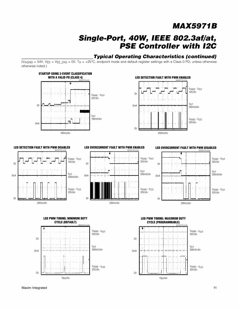
Typical Operating Characteristics (continued)(VAGND = 54V, VEE = VEE_DIG = 0V, TA = +25NC, endpoint mode and default register settings with a Class 0 PD, unless otherwise otherwise noted.)
LED PWM TIMING: MINIMUM DUTYCYCLE (DEFAULT)
MAX5971B toc24a
VAGND - VOUT50V/div
VAGND - VLED20V/div
IOUT500mA/div
OV
OmA
OV
10µs/div
LED PWM TIMING: MAXIMUM DUTYCYCLE (PROGRAMMABLE)
MAX5971B toc24b
VAGND - VOUT50V/div
VAGND - VLED20V/div
IOUT500mA/div
OV
OmA
OV
10µs/div
LED OVERCURRENT FAULT WITH PWM DISABLEDMAX5971B toc23b
200ms/div
0V
0V
0mA
VAGND - VOUT50V/div
VAGND - VLED20V/div
IOUT500mA/div
LED OVERCURRENT FAULT WITH PWM ENABLEDMAX5971B toc23a
200ms/div
0V
0V
0mA
VAGND - VOUT50V/div
VAGND - VLED20V/div
IOUT500mA/div
LED DETECTION FAULT WITH PWM DISABLEDMAX5971B toc22b
200ms/div
0V
0V
0mA
VAGND - VOUT10V/div
VAGND - VLED20V/div
IOUT500mA/div
LED DETECTION FAULT WITH PWM ENABLEDMAX5971B toc22a
200ms/div
0V
0V
0mA
VAGND - VOUT10V/div
VAGND - VLED20V/div
IOUT500mA/div
STARTUP USING 2-EVENT CLASSIFICATIONWITH A VALID PD (CLASS 4)
MAX5971B toc21
100ms/div
0V
0mA
VAGND - VOUT20V/div
IOUT100mA/div

12 Maxim Integrated
Single-Port, 40W, IEEE 802.3af/at, PSE Controller with I2C
MAX5971B
Pin Description
Pin Configuration
26
27
25
24
10
9
11
V EE
ILIM
1
ILIM
2
PWM
EN
MID
SPAN
12
V EE
N.C.
N.C.
LED
AGND
N.C.
I.C.
1 2
OUTP
4 5 6 7
2021 19 17 16 15
OUT
OUT
VEE_DIG
AD0
INT
SCL
MAX5971B
V EE
OSC
3
18
28 8N.C. SDA
N.C.
23 13 LEGACYDET
22 14 EN
*CONNECT TO VEE.
*EP
N.C.
THIN QFN
TOP VIEW
+
PIN NAME FUNCTION
1, 2, 3 VEEAnalog Low-Side Supply Input. Bypass with an external 100V, 47FF capacitor in parallel with a 100V, 0.1FF ceramic capacitor between AGND and VEE.
4 ILIM1
Class 5 Current-Limit Digital Adjust 1. Referenced to VEE. ILIM1 is internally pulled up to the digital supply. Use ILIM1 with ILIM2 to enable Class 5 operation and to adjust the Class 5 current-limit value. See the Electrical Characteristics table and Table 3 in the Class 5 PD Classification section for details.
5 ILIM2
Class 5 Current-Limit Digital Adjust 2. Referenced to VEE. ILIM2 is internally pulled up to the digital supply. Use ILIM2 with ILIM1 to enable Class 5 operation and to adjust the Class 5 current-limit value. See the Electrical Characteristics table and Table 3 in the Class 5 PD Classification section for details.
6 PWMENPWM Control Logic Input. Referenced to VEE. PWMEN is internally pulled up to the digital supply. Leave unconnected to enable the internal PWM to drive the LED pin. Force low to disable the internal PWM.
7 MIDSPAN
Detection Collision Avoidance Logic Input. Referenced to VEE. MIDSPAN is internally pulled up to the digital supply. Leave unconnected to activate the detection collision avoidance circuitry for midspan PSE systems. Force low to disable this function for an end-point PSE system. The MIDSPAN logic level latches after the device is powered up or after a reset condition.
8 SDA2-Wire Serial Interface Input/Output Data Line. Referenced to VEE. Connect to VEE if the I2C interface is not used.

13Maxim Integrated
Single-Port, 40W, IEEE 802.3af/at, PSE Controller with I2C
MAX5971B
Pin Description (continued)
PIN NAME FUNCTION
9 SCL2-Wire Serial Interface Input Clock Line. Referenced to VEE. Connect to VEE if the I2C interface is not used.
10 INTOpen-Drain Interrupt Output. Referenced to VEE. INT is pulled low whenever an interrupt is sent to the microcontroller. See the Interrupt section for details. Connect to VEE if the I2C interface is not used.
11 AD0Address Input. Referenced to VEE. AD0 is used to form the lower part of the device address. See the Device Address (AD0) section and Table 5 for details. Connect to VEE if the I2C interface is not used.
12 VEE_DIG Digital Low-Side Supply Input. Connect to VEE externally.
13 LEGACYLegacy Detection Logic Input. Referenced to VEE. LEGACY is internally pulled up to the digital supply. Leave unconnected to activate the legacy PD detection. Force low to disable this function. The LEGACY logic level latches after the device is powered up or after a reset condition.
14 EN
Enable Input. Referenced to VEE. EN is internally pulled up to the digital supply. Leave unconnected to enable the device. Force low for at least 40Fs to reset the device. The MIDSPAN, OSC, and LEGACY states latch-in when the reset condition is removed (low-to-high transition). Bypass EN to VEE with a 1nF ceramic capacitor.
15 I.C. Internally Connected. Connect I.C. to VEE.
16, 18, 20, 22, 24, 28
N.C. No Connection. Not internally connected. Leave N.C. unconnected.
17 LED
LED Indicator Open-Drain Output. Referenced to VEE. LED can sink 10mA and can drive an external LED directly. Blinking functionality is provided to signal different conditions (see the PWM and LED Signals section). Connect LED to AGND externally (see Figures 15 and 16) or to an external supply (if available) through a series resistance.
19 OSC
AC-Disconnect Triangular Wave Output. Bypass with a 100nF (Q10% tolerance) external capacitor to VEE to enable the AC disconnect function. Connect OSC to VEE to disable the AC disconnect function and to activate the DC disconnect function. The OSC state latches after the device is powered up or after a reset condition.
21 AGND High-Side Supply Input
23 DET
Detection/Classification Voltage Output. DET is used to set the detection and classification probe voltages and for the AC current sensing when using the AC disconnect function. To use the AC disconnect function, place a 1kI and 0.47FF RC series in parallel with the external protection diode to OUTP (see Figure 16).
25 OUTP
Port Pullup Output. OUTP is used to pull up the port voltage to AGND when needed. If AC disconnect is used, connect OUTP to the anode of the AC-blocking diode. If AC disconnect is not used, connect OUTP to OUT (see Figures 15 and 17). Bypass OUTP to AGND with a 100V, 0.1FF ceramic capacitor.
26, 27 OUTIntegrated MOSFET Output. If DC disconnect is used, connect the port output to OUTP (see Figures 15 and 17). If the AC disconnect function is used, connect OUT to the cathode of the AC-blocking diode (see Figure 16).
— EP Exposed Pad. Connect EP to VEE externally. See the Layout Procedure section for details.
14 Maxim Integrated
Single-Port, 40W, IEEE 802.3af/at, PSE Controller with I2C
MAX5971B
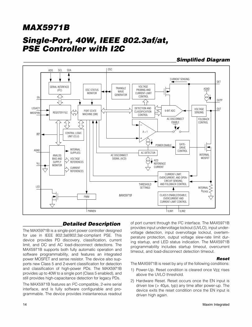
Simplified Diagram
Detailed DescriptionThe MAX5971B is a single-port power controller designed for use in IEEE 802.3af/802.3at-compliant PSE. This device provides PD discovery, classification, current limit, and DC and AC load-disconnect detections. The MAX5971B supports both fully automatic operation and software programmability, and features an integrated power MOSFET and sense resistor. The device also sup-ports new Class 5 and 2-event classification for detection and classification of high-power PDs. The MAX5971B provides up to 40W to a single port (Class 5 enabled), and still provides high-capacitance detection for legacy PDs.
The MAX5971B features an I2C-compatible, 2-wire serial interface, and is fully software configurable and pro-grammable. The device provides instantaneous readout
of port current through the I2C interface. The MAX5971B provides input undervoltage lockout (UVLO), input under-voltage detection, input overvoltage lockout, overtem-perature protection, output voltage slew-rate limit dur-ing startup, and LED status indication. The MAX5971B programmability includes startup timeout, overcurrent timeout, and load-disconnect detection timeout.
ResetThe MAX5971B is reset by any of the following conditions:
1) Power-Up. Reset condition is cleared once VEE rises above the UVLO threshold.
2) Hardware Reset. Reset occurs once the EN input is driven low (> 40Fs, typ) any time after power-up. The device exits the reset condition once the EN input is driven high again.
OSC STATUSMONITOR
SERIAL INTERFACE (I2C)
OSCADO
LEGACY
EN
MIDSPAN
INT
PORT STATEMACHINE (SM)
REGISTER FILE
ANALOGBIAS ANDSUPPLY
MONITOR
VOLTAGE PROBING AND
CURRENT-LIMITCONTROL
DETECTION ANDCLASSIFICATION
CONTROL
CENTRAL LOGICUNIT (CLU)
AC DETECTOR
PWM
AC DISCONNECTSIGNAL (ACD)
POWER ENABLE
THRESHOLDSETTINGS
ACDREFERENCECURRENT
INTERNALMOSFET
INTERNALRSENSE
VOLTAGESENSING
GATE-DRIVE
CONTROL
CURRENT-LIMIT,OVERCURRENT, AND OPEN-
CIRCUIT SENSING,AND FOLDBACK CONTROL
CLASS 5 ENABLE/DISABLE,OVERCURRENT AND
CURRENT-LIMIT CONTROL
ILIM1PWMEN
LED
VEE
AGND
ILIM2
9-BIT ADC
AGND
OUTP
OUT
FOLDBACKCONTROL
DET
TRIANGLEWAVE
GENERATOR
AC DISCONNECTENABLE
A = 1
VOLTAGEREFERENCES
CURRENTREFERENCES
INTERNALSUPPLIES
CURRENT SENSING
MAX5971B
SCL SDA

15Maxim Integrated
Single-Port, 40W, IEEE 802.3af/at, PSE Controller with I2C
MAX5971B
3) Software Reset. To initiate a software reset, write a logical 1 to the RESET_IC register (R1Ah[4]) any time after power-up. Reset clears automatically and all registers are set to their default states.
4) Thermal Shutdown. The device enters thermal shut-down at 150NC. The device exits thermal shutdown and is reset once the temperature drops below 130NC.
At the end of a reset event, the MAX5971B latches in the state of MIDSPAN, LEGACY, and OSC. During nor-mal operation, changes to the MIDSPAN and LEGACY inputs are ignored, and these inputs can be changed at any time prior to the end of a reset state. Changes to OSC input during normal operation can impact device functionality. Therefore, OSC is only changed while the device is held in a reset state (or powered down), and OSC then latches in when the reset state ends (other schematic modifications may be needed, see Figures 15 and 16).
Port ResetSet RESET_P (R1Ah[0]) high anytime during normal operation to turn off port power and clear the port event and status registers. Port reset does not initiate a global device reset.
Midspan ModeIn midspan mode, the device adopts cadence timing dur-ing the detection phase. When cadence timing is enabled and a failed detection occurs, the port waits between 2s and 2.4s before attempting to detect again. Midspan mode is activated by setting MIDSPAN high and then powering or resetting the device. Alternatively, midspan mode is software enabled by setting BCKOFF (R15h[0], Table 23) to a logical 1. By default, the MIDSPAN input is internally pulled high, enabling cadence timing. Force MIDSPAN low to disable this function.
Operation ModesThe MAX5971B provides four operating modes to suit dif-ferent system requirements. By default, auto mode allows the device to operate automatically at its default settings without any software. Semiautomatic mode automatically detects and classifies a device connected to the port after initial software activation, but does not power up the port until instructed to by software. Manual mode allows total software control of the device and is useful for sys-tem diagnostics. Shutdown mode terminates all activities and securely turns off power to the port.
Switching between auto, semiautomatic, and manual mode does not interfere with the operation of the out-put port. When the port is set into shutdown mode, all
port operations are immediately stopped and the port remains idle until shutdown mode is exited.
Auto (Automatic) ModeBy default, the MAX5971B enters auto mode after the reset condition is cleared. To manually place the MAX5971B into auto mode from any other mode, set P_M[1:0] (R12h[1:0]) to [11] during normal operation (see Tables 19 and 20).
In auto mode, the MAX5971B performs detection and classification, and powers up the port automatically if a valid PD is connected to the port. If a valid PD is not con-nected at the port, the MAX5971B repeats the detection routine continuously until a valid PD is connected.
When entering auto mode, the DET_EN and CLASS_EN bits (R14h[0] and R14h[4], Table 22) are set to high and stay high unless changed by software. Using soft-ware to set DET_EN and/or CLASS_EN low causes the MAX5971B to skip detection and/or classification. As a protection, disabling the detection routine in auto mode does not allow the corresponding port to power up, unless the DET_BY bit (R23h[4], Table 33) is set to 1.
Semiautomatic (Semi) ModeThe MAX5971B is put into semiautomatic mode by set-ting P_M[1:0] (R12h[1:0]) to [10] during normal operation (see Tables 19 and 20). In semi mode, the MAX5971B, upon request, performs detection and/or classification repeatedly but does not power up the port. To power the port, set the PWR_ON bit (R19h[0], Table 27) to 1. This immediately terminates the detection/classification routine and turns on power to the port.
DET_EN and CLASS_EN (R14h[0] and R14h[4], Table 22) default to low in semiautomatic mode. Use software to set DET_EN (R14h[0]) to 1 to start the detection routine and CLASS_EN (R14h[4]) to 1 to enable classification routine. They are reset every time the software commands a power-off of the port, either through a reset event or by writing a 1 to the PWR_OFF bit (R19h[4]). In any other case, the status of the bits is left unchanged (including when the state machine turns off the power when a load disconnect or a fault condition is encountered).
Manual ModeThe MAX5971B is placed in manual mode by setting P_M[1:0] (R12h[1:0]) to [01] during normal operation (see Tables 19 and 20). Manual mode allows the soft-ware to dictate the sequence of operation. Write a 1 to both R14h[0] (DET_EN) and R14h[4] (CLASS_EN) to start detection and classification operations, respec-tively, and in that priority order. In manual mode, after
16 Maxim Integrated
Single-Port, 40W, IEEE 802.3af/at, PSE Controller with I2C
MAX5971B
execution, the command is cleared from the register(s). PWR_ON has highest priority. Setting PWR_ON to 1 at any time causes the device to immediately enter the powered mode. Setting DET_EN and CLASS_EN to 1 at the same time causes detection to be performed first. Once in the powered state, the device ignores DET_EN or CLASS_EN commands.
When switching to manual mode from another mode, DET_EN and CLASS_EN default to low. These bits become pushbutton rather than configuration bits. Writing 1 to these bits while in manual mode commands the device to execute one cycle of detection and/or classifica-tion. They are reset back to 0 at the end of the execution.
Shutdown ModeTo put the MAX5971B into shutdown mode, set P_M[1:0] (R12h[1:0]) to [00] during normal operation (see Table 19 and Table 20). Putting the MAX5971B into shutdown mode immediately turns off port power, clears the event and sta-tus bits, and halts all port operations. In shutdown mode the serial interface is still fully active, however, all DET_EN, CLASS_EN, and PWR_ON commands are ignored.
PD DetectionDuring normal operation, the MAX5971B probes the output for a valid PD. A valid PD has a 25kI discov-ery signature characteristic as specified in the IEEE 802.3af/802.3at standard. Table 1 shows the IEEE 802.3at specification for a PSE detecting a valid PD signature.
After each detection cycle, the MAX5971B sets DET_END (R04h[0] and R05h[0]) to 1 and reports the detec-tion results in the detection status bits, DET_ST[2:0]
(R0Ch[2:0], see Table 14). The DET_END registers are reset to 0 when read through the CoR (clear-on-read) register R05h[0], or after a reset event.
During detection, the MAX5971B keeps the internal MOSFET off and forces two probe voltages through DET. The current through DET is measured as well as the volt-age at OUT. A two-point slope measurement is used, as specified by the IEEE 802.3af/802.3at standard, to verify the device connected to the port. By default, The MAX5971B load stability check is disabled. Set LSC_EN (R29h[4], Table 36) to 1 to enable the load stability check. The MAX5971B implements appropriate settling times to reject 50Hz/60Hz power-line noise coupling.
An external diode, in series with the DET input, restricts PD detection to the first quadrant as specified by the IEEE 802.3af/802.3at standard. To prevent damage to non-PD devices, and to protect itself from an output short circuit, the MAX5971B limits the current into DET to less than 2mA (max) during PD detection.
In midspan mode, after every failed detection cycle, the MAX5971B waits at least 2.0s before attempting another detection cycle. The first detection, however, still hap-pens immediately after exiting a reset condition.
High-Capacitance DetectionHigh-capacitance detection for legacy PDs is both soft-ware and pin programmable (LEGACY). To use software to enable high-capacitance detection, set CLC_EN (R23h[5]) to 1 during normal operation. Alternatively, the status of the LEGACY input is latched and writ-ten to CLC_EN during power-up or after reset condi- tion is cleared. The LEGACY input is internally pulled
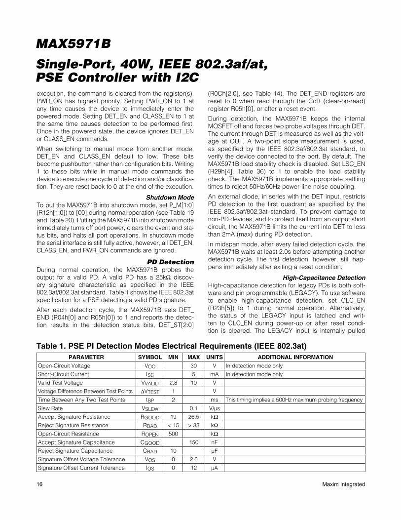
Table 1. PSE PI Detection Modes Electrical Requirements (IEEE 802.3at)PARAMETER SYMBOL MIN MAX UNITS ADDITIONAL INFORMATION
Open-Circuit Voltage VOC 30 V In detection mode only
Short-Circuit Current ISC 5 mA In detection mode only
Valid Test Voltage VVALID 2.8 10 V
Voltage Difference Between Test Points DVTEST 1 V
Time Between Any Two Test Points tBP 2 ms This timing implies a 500Hz maximum probing frequency
Slew Rate VSLEW 0.1 V/Fs
Accept Signature Resistance RGOOD 19 26.5 kI
Reject Signature Resistance RBAD < 15 > 33 kI
Open-Circuit Resistance ROPEN 500 kI
Accept Signature Capacitance CGOOD 150 nF
Reject Signature Capacitance CBAD 10 FF
Signature Offset Voltage Tolerance VOS 0 2.0 V
Signature Offset Current Tolerance IOS 0 12 FA
17Maxim Integrated
Single-Port, 40W, IEEE 802.3af/at, PSE Controller with I2C
MAX5971B
high, enabling high-capacitance detection. Unless high-capacitance detection is needed, connect LEGACY to VEE to disable this function. If high-capacitance detection is enabled, PD signature capacitances up to 47FF (typ) are accepted.
Powered Device Classification (PD Classification)
During PD classification, the MAX5971B forces a probe voltage (-18V, typ) at DET and measures the current into DET. The measured current determines the class of the PD.
After each classification cycle, the MAX5971B sets CL_END (R04h[4] and R05h[4]) to 1 and reports the classification results in the classification status bits, CLASS[2:0] (R0Ch[6:4], see Table 14). The CL_END "registers are reset to 0 when read through the CoR (clear- on-read) register, R05h, or after a reset event.
If ILIM1 and ILIM2 are both left unconnected, the MAX5971B classifies the PD based on Table 33.9 of the IEEE 802.3at standard (see Table 2). If the measured
current exceeds 51mA, the MAX5971B does not power the PD, but returns to idle state before attempting a new detection cycle.
Class 5 PD ClassificationThe MAX5971B supports high power beyond the IEEE 802.3at standard by providing an additional classifica-tion (Class 5) if needed. To enable Class 5 detection and select the corresponding current-limit/overcurrent thresholds, ILIM1 and ILIM2 must be set based on the combinations detailed in Table 3. Once Class 5 is enabled, during classification, if the MAX5971B detects currents in excess of the Class 4 upper limit threshold, the PD is classified as a Class 5 powered device. The PD is guaranteed to be classified as a Class 5 device for any classification current from 51mA up to the classification current-limit threshold.
The Class 5 overcurrent threshold and current limit is set with ILIM1 and ILIM2. ILIM1 and ILIM2 are both referenced to VEE and are internally pulled up to the digital supply. Leave ILIM1 and ILIM2 unconnected to disable Class 5 detection and to be fully compliant to IEEE 802.3at standard classification. Class 5 detection is enabled, and the corresponding overcurrent threshold and current limit is adjusted, by connecting one or both to VEE (see Table 3).
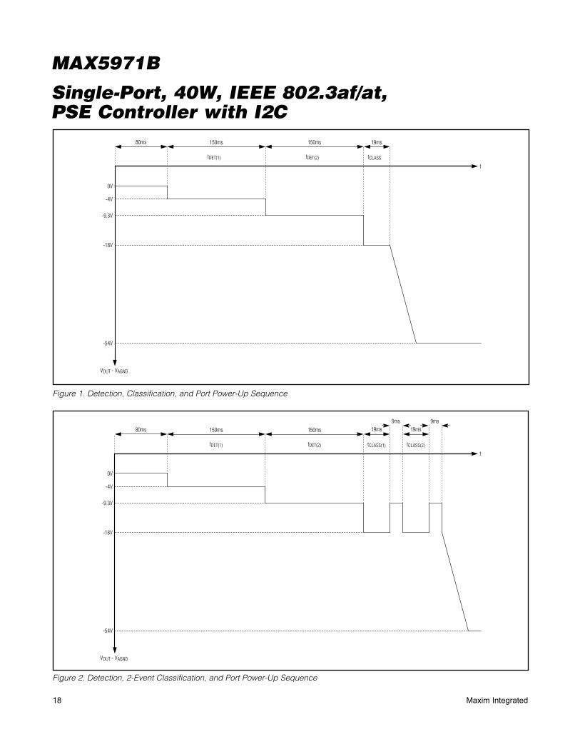
2-Event PD ClassificationIf the result of the first classification event is Class 0 through Class 3, then only a single classification event occurs as shown in Figure 1. However, if the result is Class 4 or Class 5 (when enabled), the device performs a second classification event as shown in Figure 2. Between the classification cycles, the MAX5971B per-forms a first and second mark event as required by the IEEE 802.3at standard, forcing a -9.3V probing voltage at DET.
Table 2. PSE Classification of a PD (Table 33.9 of the IEEE 802.3at Standard)
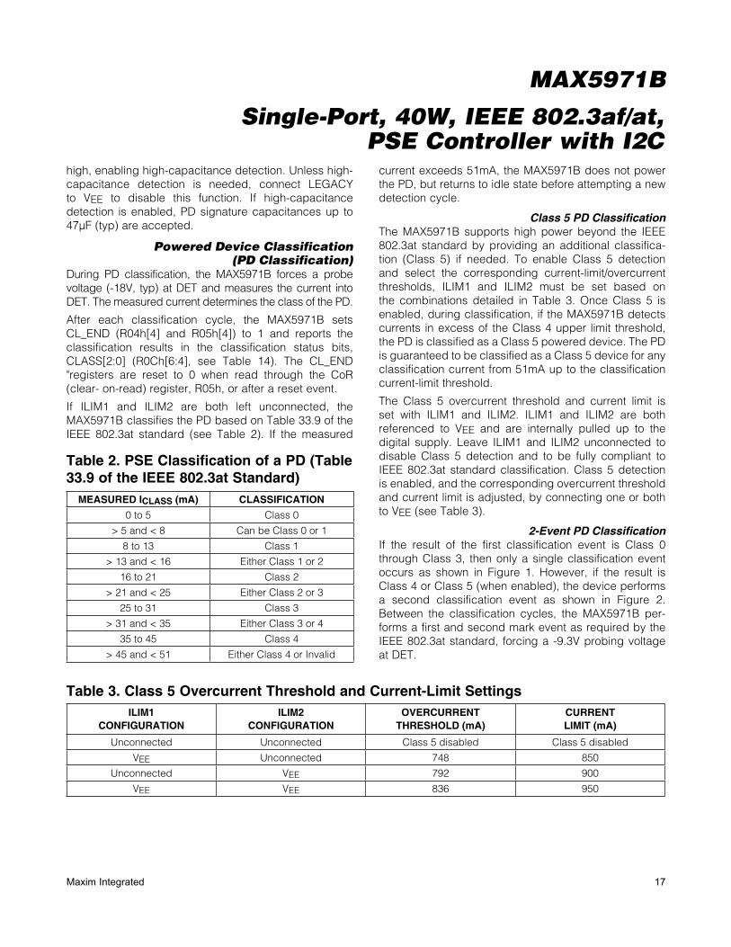
Table 3. Class 5 Overcurrent Threshold and Current-Limit Settings
MEASURED ICLASS (mA) CLASSIFICATION
0 to 5 Class 0
> 5 and < 8 Can be Class 0 or 1
8 to 13 Class 1
> 13 and < 16 Either Class 1 or 2
16 to 21 Class 2
> 21 and < 25 Either Class 2 or 3
25 to 31 Class 3
> 31 and < 35 Either Class 3 or 4
35 to 45 Class 4
> 45 and < 51 Either Class 4 or Invalid
ILIM1 CONFIGURATION
ILIM2 CONFIGURATION
OVERCURRENT THRESHOLD (mA)
CURRENTLIMIT (mA)
Unconnected Unconnected Class 5 disabled Class 5 disabled
VEE Unconnected 748 850
Unconnected VEE 792 900
VEE VEE 836 950
18 Maxim Integrated
Single-Port, 40W, IEEE 802.3af/at, PSE Controller with I2C
MAX5971B
Figure 1. Detection, Classification, and Port Power-Up Sequence
Figure 2. Detection, 2-Event Classification, and Port Power-Up Sequence
VOUT - VAGND
t
0V
-4V
-9.3V
-18V
-54V
tDET(1) tDET(2) tCLASS
80ms 150ms 150ms 19ms
VOUT - VAGND
t
0V
-4V
-9.3V
-18V
-54V
tDET(1) tDET(2) tCLASS(1) tCLASS(2)
80ms 150ms 150ms 19ms 19ms
9ms 9ms
19Maxim Integrated
Single-Port, 40W, IEEE 802.3af/at, PSE Controller with I2C
MAX5971B
Powered StateWhen the MAX5971B enters a powered state, the tFAULT and tDISC timers are reset. When the startup timer (tSTART) has timed out, the device enters a normal powered condition, allowing power delivery to the PD. PGOOD (R10h[4], Table 17) is set to 1 when the device enters the normal powered condition. PGOOD immedi-ately resets to 0 whenever the power to the port is turned off. The power-good change bits, PG_CHG (R02h[4] and R03h[4], Table 9) are set both when the port powers up and when it powers down. PWR_EN (R10h[0], Table 17) is set to 1 when the port powers up and resets to 0 when a port shuts down. Set PWR_OFF (R19h[4], Table 27) to 1 to immediately turn off power to the port.
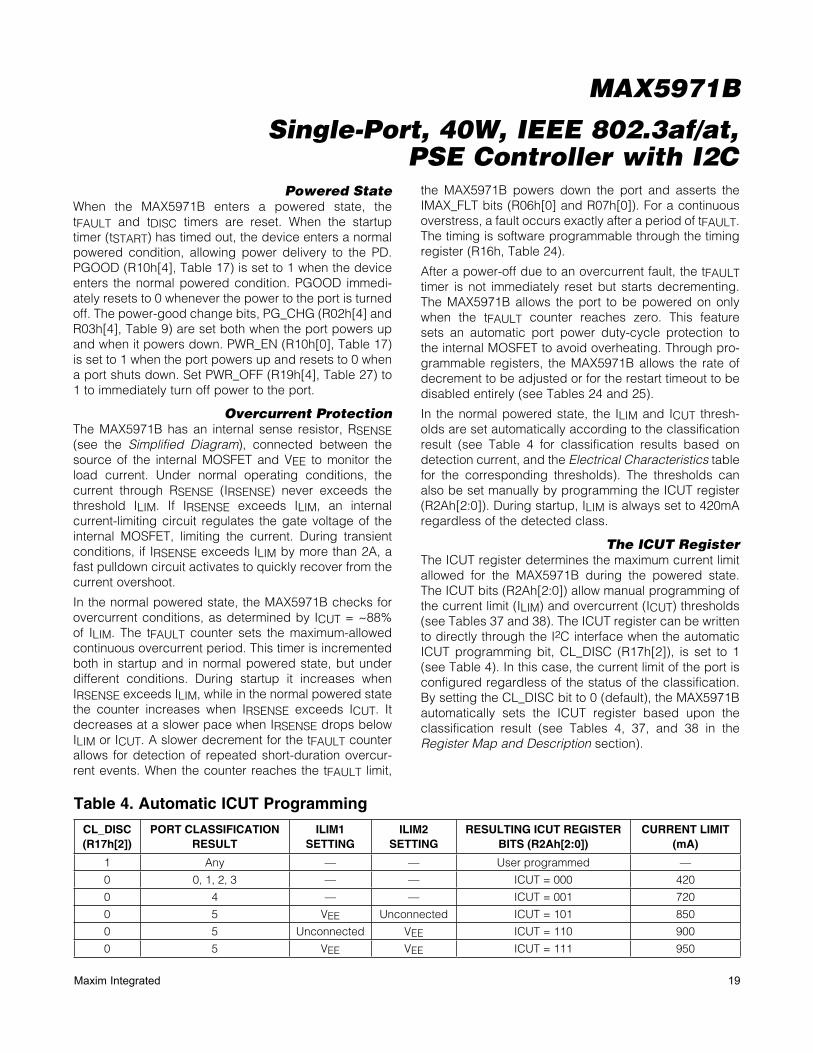
Overcurrent ProtectionThe MAX5971B has an internal sense resistor, RSENSE (see the Simplified Diagram), connected between the source of the internal MOSFET and VEE to monitor the load current. Under normal operating conditions, the current through RSENSE (IRSENSE) never exceeds the threshold ILIM. If IRSENSE exceeds ILIM, an internal current-limiting circuit regulates the gate voltage of the internal MOSFET, limiting the current. During transient conditions, if IRSENSE exceeds ILIM by more than 2A, a fast pulldown circuit activates to quickly recover from the current overshoot.
In the normal powered state, the MAX5971B checks for overcurrent conditions, as determined by ICUT = ~88% of ILIM. The tFAULT counter sets the maximum-allowed continuous overcurrent period. This timer is incremented both in startup and in normal powered state, but under different conditions. During startup it increases when IRSENSE exceeds ILIM, while in the normal powered state the counter increases when IRSENSE exceeds ICUT. It decreases at a slower pace when IRSENSE drops below ILIM or ICUT. A slower decrement for the tFAULT counter allows for detection of repeated short-duration overcur-rent events. When the counter reaches the tFAULT limit,
the MAX5971B powers down the port and asserts the IMAX_FLT bits (R06h[0] and R07h[0]). For a continuous overstress, a fault occurs exactly after a period of tFAULT. The timing is software programmable through the timing register (R16h, Table 24).
After a power-off due to an overcurrent fault, the tFAULT timer is not immediately reset but starts decrementing. The MAX5971B allows the port to be powered on only when the tFAULT counter reaches zero. This feature sets an automatic port power duty-cycle protection to the internal MOSFET to avoid overheating. Through pro-grammable registers, the MAX5971B allows the rate of decrement to be adjusted or for the restart timeout to be disabled entirely (see Tables 24 and 25).
In the normal powered state, the ILIM and ICUT thresh-olds are set automatically according to the classification result (see Table 4 for classification results based on detection current, and the Electrical Characteristics table for the corresponding thresholds). The thresholds can also be set manually by programming the ICUT register (R2Ah[2:0]). During startup, ILIM is always set to 420mA regardless of the detected class.
The ICUT RegisterThe ICUT register determines the maximum current limit allowed for the MAX5971B during the powered state. The ICUT bits (R2Ah[2:0]) allow manual programming of the current limit (ILIM) and overcurrent (ICUT) thresholds (see Tables 37 and 38). The ICUT register can be written to directly through the I2C interface when the automatic ICUT programming bit, CL_DISC (R17h[2]), is set to 1 (see Table 4). In this case, the current limit of the port is configured regardless of the status of the classification. By setting the CL_DISC bit to 0 (default), the MAX5971B automatically sets the ICUT register based upon the classification result (see Tables 4, 37, and 38 in the Register Map and Description section).
Table 4. Automatic ICUT Programming
CL_DISC (R17h[2])
PORT CLASSIFICATION RESULT
ILIM1SETTING
ILIM2SETTING
RESULTING ICUT REGISTER BITS (R2Ah[2:0])
CURRENT LIMIT (mA)
1 Any — — User programmed —
0 0, 1, 2, 3 — — ICUT = 000 420
0 4 — — ICUT = 001 720
0 5 VEE Unconnected ICUT = 101 850
0 5 Unconnected VEE ICUT = 110 900
0 5 VEE VEE ICUT = 111 950

20 Maxim Integrated
Single-Port, 40W, IEEE 802.3af/at, PSE Controller with I2C
MAX5971B
Foldback CurrentDuring startup and normal operation, an internal circuit senses the port voltage and reduces the current-limit value and the overcurrent threshold when (VAGND - VOUT) < 27V. The foldback function helps to reduce the power dissipation on the internal MOSFET. The current limit eventually reduces down to ITH_FB (166mA, typ) when (VAGND - VOUT) < 10V (see Figure 3).
Digital LogicThe MAX5971B internally generates digital supplies (referenced to VEE) to power the internal logic circuitry. All logic inputs and outputs are referenced to VEE. See the Electrical Characteristics table for digital input thresholds. If digital logic inputs are driven externally, the nominal digital logic level is 3.3V.
InterruptThe MAX5971B contains an open-drain logic output (INT) that goes low when an interrupt condition exists. The interrupt register (R00h, Table 7) contains the inter-rupt flag bits and the interrupt mask register (R01h, Table 8) determines which events can trigger an inter-rupt. When an event occurs, the appropriate interrupt event register bits (in R02h through R0Bh) and the cor-responding interrupt (in R00h) are set to 1 and INT is asserted low (unless masked).
As a response to an interrupt, the controller can read the status of the event register(s) to determine the cause of the interrupt and take appropriate action. Each inter-rupt event register is paired with a clear-on-read (CoR) register. When an interrupt event register is read through the corresponding CoR register, the interrupt register is reset to 0. INT remains low and the interrupt is not reset when the interrupt event register is read through the read-only addresses. For example, to clear a sup-ply event fault, read R0Bh (CoR) not R0Ah (read only, see Table 13). Use the CLR_INT bit (R1Ah[7]) to clear an interrupt, or the RESET_IC (R1Ah[4]) or RESET_P (R1Ah[0]) bit to initiate a software reset (see Table 28).
Undervoltage and Overvoltage ProtectionThe MAX5971B contains both undervoltage and over-voltage protection features. Table 13 in the Register Map and Description section shows a detailed list of the undervoltage and overvoltage protection features. An internal VEE undervoltage lockout (VEE_UVLO) cir-cuit keeps the port off and the MAX5971B in reset until VAGND - VEE exceeds 28.5V (typ) for more than 2.5ms. An internal VEE overvoltage (VEE_OV) circuit shuts down the port when VAGND - VEE exceeds 62.5V (typ). The MAX5971B also features a VEE undervoltage interrupt (VEE_UV) that triggers when VAGND - VEE drops below
Figure 3. Foldback Current Characteristics
VAGND - VOUT
ILIM
ITH_FB
10V 27V
IRSENSE
21Maxim Integrated
Single-Port, 40W, IEEE 802.3af/at, PSE Controller with I2C
MAX5971B
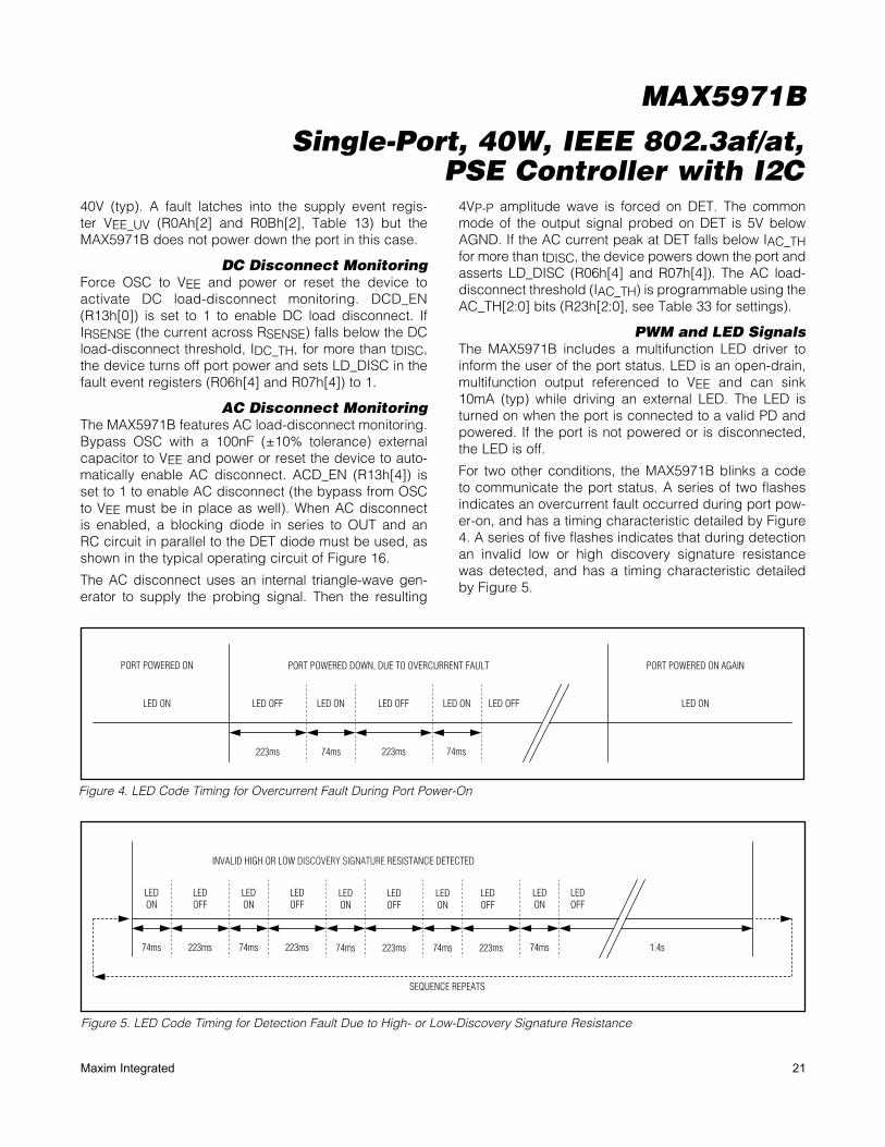
Figure 4. LED Code Timing for Overcurrent Fault During Port Power-On
Figure 5. LED Code Timing for Detection Fault Due to High- or Low-Discovery Signature Resistance
40V (typ). A fault latches into the supply event regis-ter VEE_UV (R0Ah[2] and R0Bh[2], Table 13) but the MAX5971B does not power down the port in this case.
DC Disconnect MonitoringForce OSC to VEE and power or reset the device to activate DC load-disconnect monitoring. DCD_EN (R13h[0]) is set to 1 to enable DC load disconnect. If IRSENSE (the current across RSENSE) falls below the DC load-disconnect threshold, IDC_TH, for more than tDISC, the device turns off port power and sets LD_DISC in the fault event registers (R06h[4] and R07h[4]) to 1.
AC Disconnect MonitoringThe MAX5971B features AC load-disconnect monitoring. Bypass OSC with a 100nF (Q10% tolerance) external capacitor to VEE and power or reset the device to auto-matically enable AC disconnect. ACD_EN (R13h[4]) is set to 1 to enable AC disconnect (the bypass from OSC to VEE must be in place as well). When AC disconnect is enabled, a blocking diode in series to OUT and an RC circuit in parallel to the DET diode must be used, as shown in the typical operating circuit of Figure 16.
The AC disconnect uses an internal triangle-wave gen-erator to supply the probing signal. Then the resulting
4VP-P amplitude wave is forced on DET. The common mode of the output signal probed on DET is 5V below AGND. If the AC current peak at DET falls below IAC_TH for more than tDISC, the device powers down the port and asserts LD_DISC (R06h[4] and R07h[4]). The AC load-disconnect threshold (IAC_TH) is programmable using the AC_TH[2:0] bits (R23h[2:0], see Table 33 for settings).
PWM and LED SignalsThe MAX5971B includes a multifunction LED driver to inform the user of the port status. LED is an open-drain, multifunction output referenced to VEE and can sink 10mA (typ) while driving an external LED. The LED is turned on when the port is connected to a valid PD and powered. If the port is not powered or is disconnected, the LED is off.
For two other conditions, the MAX5971B blinks a code to communicate the port status. A series of two flashes indicates an overcurrent fault occurred during port pow-er-on, and has a timing characteristic detailed by Figure 4. A series of five flashes indicates that during detection an invalid low or high discovery signature resistance was detected, and has a timing characteristic detailed by Figure 5.
LED OFFLED ON
223ms
LED ON LED ON LED ONLED OFF LED OFF
74ms 74ms223ms
PORT POWERED DOWN, DUE TO OVERCURRENT FAULTPORT POWERED ON PORT POWERED ON AGAIN
LEDOFF
LEDON
223ms74ms
LEDOFF
LEDON
223ms74ms
LEDOFF
LEDON
223ms74ms
LEDOFF
LEDON
223ms74ms
LEDON
74ms
LEDOFF
1.4s
SEQUENCE REPEATS
INVALID HIGH OR LOW DISCOVERY SIGNATURE RESISTANCE DETECTED
22 Maxim Integrated
Single-Port, 40W, IEEE 802.3af/at, PSE Controller with I2C
MAX5971B
The MAX5971B also contains an internal square wave, PWM signal generator. The PWM runs at a typical fre-quency of 25kHz with a default duty cycle of 6.25%. The duty cycle is programmable from 6.25% up to 25% through the PWM_TH[1:0] bits (R24h[5:4], Tables 34 and 35). PWMEN is used to enable or disable the PWM. PWMEN is internally pulled up to the digital supply, and can be left unconnected to enable the internal PWM. When enabled, the LED pulses are driven by the PWM to reduce the power dissipation and increase the system efficiency. Force PWMEN low to disable the internal PWM; LED is then driven directly.
Thermal ShutdownIf the MAX5971B die temperature reaches +150NC (typ), an overtemperature fault is generated and the device shuts down. The die temperature must cool down below 130NC (typ) to remove the overtemperature fault con-dition. After a thermal shutdown condition clears, the device is reset.
WatchdogThe R1Eh and R1Fh registers control the watchdog operation. The watchdog function, when enabled, allows the MAX5971B to automatically take over control and securely shut down the power to the port in case of software/firmware crashes. See the Register Map and Description section for register configuration and set-tings (Tables 30, 31, and 32).
Device Address (AD0)The MAX5971B is programmable to one of four unique slave addresses. To program the device address, connect AD0 to VEE, SCL, SDA or to an external VCC supply referenced to VEE. This external VCC (at AD0)
must exceed the digital input logic-high threshold (VCC > 2.4V, see Table 5), but should not exceed 5.5V. An external regulated 3.3V or 5V supply is recommended for VCC.
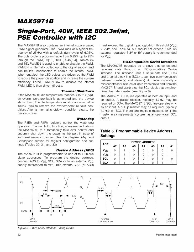
I2C-Compatible Serial InterfaceThe MAX5971B operates as a slave that sends and receives data through an I²C-compatible 2-wire interface. The interface uses a serial-data line (SDA) and a serial-clock line (SCL) to achieve communication between master(s) and slave(s). A master (typically a microcontroller) initiates all data transfers to and from the MAX5971B, and generates the SCL clock that synchro-nizes the data transfer (see Figure 6).
The MAX5971B SDA line operates as both an input and an output. A pullup resistor, typically 4.7kI, may be required on SDA. The MAX5971B SCL line operates only as an input. A pullup resistor may be required (typically 4.7kI) on SCL if there are multiple masters, or if the master in a single-master system has an open-drain SCL output.
Figure 6. 2-Wire Serial Interface Timing Details
Table 5. Programmable Device Address Settings
SDA
SCL
tSU,DAT
tHD,DATtLOW
tSU,STA
tHD,STA
tR tF
STARTCONDITION
REPEATEDSTART CONDITION
STOPCONDITION
STARTCONDITION
tHD,STA
tSU,STO
tBUF
tHIGH
AD0DEVICE ADDRESS
A7 A6 A5 A4 A3 A2 A1
VEE 0 1 0 0 0 0 0
VCC 0 1 0 0 0 0 1
SCL 0 1 0 0 0 1 0
SDA 0 1 0 0 0 1 1
23Maxim Integrated
Single-Port, 40W, IEEE 802.3af/at, PSE Controller with I2C
MAX5971B
Figure 7. START and STOP Conditions
Figure 8. Bit Transfer
Figure 9. Acknowledge
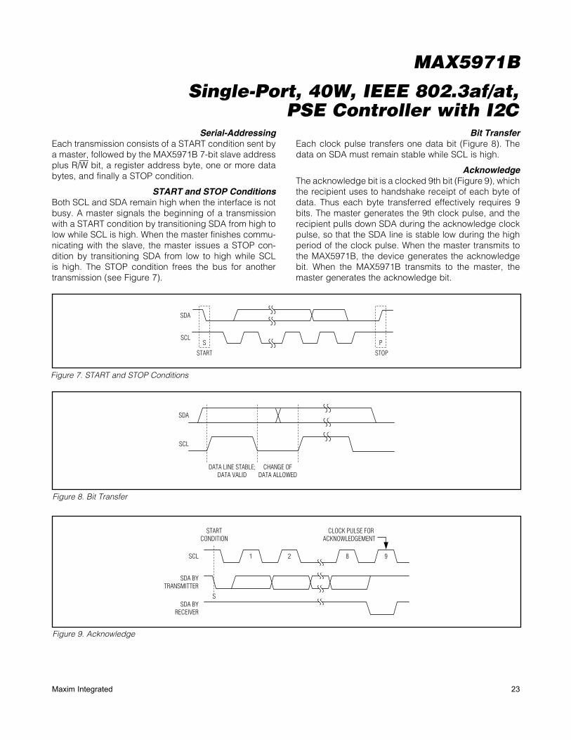
Serial-AddressingEach transmission consists of a START condition sent by a master, followed by the MAX5971B 7-bit slave address plus R/W bit, a register address byte, one or more data bytes, and finally a STOP condition.
START and STOP ConditionsBoth SCL and SDA remain high when the interface is not busy. A master signals the beginning of a transmission with a START condition by transitioning SDA from high to low while SCL is high. When the master finishes commu-nicating with the slave, the master issues a STOP con-dition by transitioning SDA from low to high while SCL is high. The STOP condition frees the bus for another transmission (see Figure 7).
Bit TransferEach clock pulse transfers one data bit (Figure 8). The data on SDA must remain stable while SCL is high.
AcknowledgeThe acknowledge bit is a clocked 9th bit (Figure 9), which the recipient uses to handshake receipt of each byte of data. Thus each byte transferred effectively requires 9 bits. The master generates the 9th clock pulse, and the recipient pulls down SDA during the acknowledge clock pulse, so that the SDA line is stable low during the high period of the clock pulse. When the master transmits to the MAX5971B, the device generates the acknowledge bit. When the MAX5971B transmits to the master, the master generates the acknowledge bit.
SDA
SCLS
START STOP
P
SDA
SCL
DATA LINE STABLE;DATA VALID
CHANGE OFDATA ALLOWED
SCL
SDA BYTRANSMITTER
SDA BYRECEIVER
STARTCONDITION
1
S
2 8 9
CLOCK PULSE FOR ACKNOWLEDGEMENT
24 Maxim Integrated
Single-Port, 40W, IEEE 802.3af/at, PSE Controller with I2C
MAX5971B
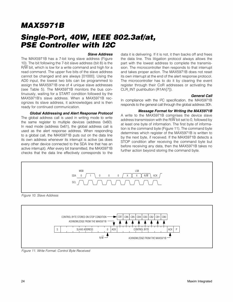
Slave AddressThe MAX5971B has a 7-bit long slave address (Figure 10). The bit following the 7-bit slave address (bit 8) is the R/W bit, which is low for a write command and high for a read command. The upper five bits of the slave address cannot be changed and are always [01000]. Using the AD0 input, the lowest two bits can be programmed to assign the MAX5971B one of 4 unique slave addresses (see Table 5). The MAX5971B monitors the bus con-tinuously, waiting for a START condition followed by the MAX5971B’s slave address. When a MAX5971B rec-ognizes its slave address, it acknowledges and is then ready for continued communication.
Global Addressing and Alert Response ProtocolThe global address call is used in writing mode to write the same register to multiple devices (address 0x60). In read mode (address 0x61), the global address call is used as the alert response address. When responding to a global call, the MAX5971B puts out on the data line its own address whenever its interrupt is active (as does every other device connected to the SDA line that has an active interrupt). After every bit transmitted, the MAX5971B checks that the data line effectively corresponds to the
data it is delivering. If it is not, it then backs off and frees the data line. This litigation protocol always allows the part with the lowest address to complete the transmis-sion. The microcontroller then responds to that interrupt and takes proper action. The MAX5971B does not reset its own interrupt at the end of the alert response protocol. The microcontroller has to do it by clearing the event register through their CoR addresses or activating the CLR_INT pushbutton (R1Ah[7]).
General CallIn compliance with the I2C specification, the MAX5971B responds to the general call through the global address 30h.
Message Format for Writing the MAX5971BA write to the MAX5971B comprises the device slave address transmission with the R/W bit set to 0, followed by at least one byte of information. The first byte of informa-tion is the command byte (Figure 11). The command byte determines which register of the MAX5971B is written to by the next byte, if received. If the MAX5971B detects a STOP condition after receiving the command byte but before receiving any data, then the MAX5971B takes no further action beyond storing the command byte.
Figure 10. Slave Address
Figure 11. Write Format: Control Byte Received
SDA 0
SCL
1 0 0 0 X
LSBMSB
X R/W ACK
R/W
CB7
S 0 PACK ACK
CB6 CB5 CB4 CB3 CB2 CB1 CB0CONTROL BYTE STORED ON STOP CONDITION
ACKNOWLEDGE FROM THE MAX5971B
SLAVE ADDRESS CONTROL BYTE
ACKNOWLEDGE FROM THE MAX5971B
25Maxim Integrated
Single-Port, 40W, IEEE 802.3af/at, PSE Controller with I2C
MAX5971B
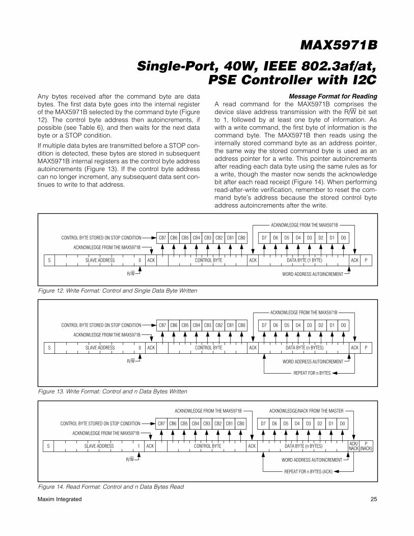
Any bytes received after the command byte are data bytes. The first data byte goes into the internal register of the MAX5971B selected by the command byte (Figure 12). The control byte address then autoincrements, if possible (see Table 6), and then waits for the next data byte or a STOP condition.
If multiple data bytes are transmitted before a STOP con-dition is detected, these bytes are stored in subsequent MAX5971B internal registers as the control byte address autoincrements (Figure 13). If the control byte address can no longer increment, any subsequent data sent con-tinues to write to that address.
Message Format for ReadingA read command for the MAX5971B comprises the device slave address transmission with the R/W bit set to 1, followed by at least one byte of information. As with a write command, the first byte of information is the command byte. The MAX5971B then reads using the internally stored command byte as an address pointer, the same way the stored command byte is used as an address pointer for a write. This pointer autoincrements after reading each data byte using the same rules as for a write, though the master now sends the acknowledge bit after each read receipt (Figure 14). When performing read-after-write verification, remember to reset the com-mand byte’s address because the stored control byte address autoincrements after the write.
Figure 12. Write Format: Control and Single Data Byte Written
Figure 13. Write Format: Control and n Data Bytes Written
Figure 14. Read Format: Control and n Data Bytes Read
R/W
CB7
S 0 ACK ACK ACK P
CB6 CB5 CB4 CB3 CB2 CB1 CB0 D7 D6 D5 D4 D3 D2 D1 D0CONTROL BYTE STORED ON STOP CONDITION
ACKNOWLEDGE FROM THE MAX5971B
SLAVE ADDRESS CONTROL BYTE DATA BYTE (1 BYTE)
WORD ADDRESS AUTOINCREMENT
ACKNOWLEDGE FROM THE MAX5971B
S 0 ACK ACK ACK PSLAVE ADDRESS CONTROL BYTE DATA BYTE (n BYTES)
CB7 CB6 CB5 CB4 CB3 CB2 CB1 CB0CONTROL BYTE STORED ON STOP CONDITION
ACKNOWLEDGE FROM THE MAX5971B
R/W
D7 D6 D5 D4 D3 D2 D1 D0
WORD ADDRESS AUTOINCREMENT
REPEAT FOR n BYTES
ACKNOWLEDGE FROM THE MAX5971B
S 1 ACK ACK ACK/NACKSLAVE ADDRESS CONTROL BYTE DATA BYTE (n BYTES)
CB7 CB6 CB5 CB4 CB3 CB2 CB1 CB0CONTROL BYTE STORED ON STOP CONDITION
ACKNOWLEDGE FROM THE MAX5971B
R/W
D7 D6 D5 D4 D3 D2 D1 D0
ACKNOWLEDGE/NACK FROM THE MASTERACKNOWLEDGE FROM THE MAX5971B
WORD ADDRESS AUTOINCREMENT
REPEAT FOR n BYTES (ACK)
P(NACK)

26 Maxim Integrated
Single-Port, 40W, IEEE 802.3af/at, PSE Controller with I2C
MAX5971B
Operation with Multiple MastersWhen the MAX5971B operates on a 2-wire interface with multiple masters, a master reading the MAX5971B should use repeated starts between the write that sets the MAX5971B’s address pointer, and the read(s) that take the data from the location(s). It is possible for master 2 to take over the bus after master 1 has set up the MAX5971B’s address pointer but before master 1 has read the data. If master 2 subsequently resets the MAX5971B’s address pointer, then master 1’s read may be from an unexpected location.
Command Address AutoincrementingAddress autoincrementing allows the MAX5971B to be configured with fewer transmissions by minimizing the number of times the command address needs to be sent. The command address stored in the MAX5971B generally increments after each data byte is written or read (Table 6). The MAX5971B is designed to prevent
overwrites on unavailable register addresses and unin-tentional wraparound of addresses.
Register Map and DescriptionThe MAX5971B contains a bank of volatile registers that store its settings and status. The device features an I2C-compatible, 2-wire serial interface, allowing the registers to be fully software configurable and programmable. In addition to this, several registers are also pin programmable to allow the MAX5971B to operate in auto mode and still be partially configurable even without the assistance of software.
The Interrupts Registers (R00h to R01h)Interrupt Register (R00h)
The interrupt register (R00h, Table 7) summarizes the event register status and is used to send an interrupt signal to the controller. On power-up or after a reset condition, interrupt (R00h) is set to a default value of 00h. INT goes low to report an interrupt event if any one of the active interrupt bits is set to 1 (active high) and it is not masked by the interrupt mask register (R01h, Table 8). INT does not go low to report an interrupt if the cor-responding mask bit (R01h) is set. Writing a 1 to CLR_INT (R1Ah[7], Table 28) clears all interrupt and events reg-isters (resets to low). INT_EN (R17h[7], Table 26) is a global interrupt enable and writing a 0 to INT_EN disables the INT output, putting it into a state of high impedance.
Table 6. Autoincrement Rules
Table 7. Interrupt Register
COMMAND BYTE ADDRESS RANGE
AUTOINCREMENT BEHAVIOR
0x00 to 0x37Command address autoincrements
after byte read or written
0x37Command address remains at 0x37
after byte written or read
ADDRESS = 00hDESCRIPTION
SYMBOL BIT NO. TYPE
SUP_INT 7 RInterrupt signal for supply faults. SUP_INT is the logic OR of all the active bits in the supply event register (R0Ah/R0Bh, Table 13).
IVC_INT 6 RInterrupt signal for class current-limit violations. IVC_INT reports the status of IVC_FLT (bit 4) in the startup event register (R08h/R09h, Table 12).
IMAX_INT 5 RInterrupt signal for current-limit violations. IMAX_INT reports the status of IMAX_FLT (bit 0) in the fault event register (R06h/R07h, Table 11).
CL_INT 4 RInterrupt signal for completion of classification. CL_INT reports the status of CL_END (bit 4) in the detect event register (R04h/R05h, Table 10).
DET_INT 3 RInterrupt signal for completion of detection. DET_INT reports the status of DET_END (bit 0) in the detect event register (R04h/R05h, Table 10).
LD_INT 2 RInterrupt signal for load disconnection. LD_INT reports the status of LD_DISC (bit 4) in the fault event register (R06h/R07h, Table 11).
PG_INT 1 RInterrupt signal for PGOOD (R10h[4]) status changes. PG_INT reports the status of PG_CHG (bit 4) in the power event register (R02h/R03h, Table 9).
PE_INT 0 RInterrupt signal for power enable status change. PE_INT reports the status of PWEN_CHG (bit 0) in the power event register (R02h/R03h, Table 9).
27Maxim Integrated
Single-Port, 40W, IEEE 802.3af/at, PSE Controller with I2C
MAX5971B
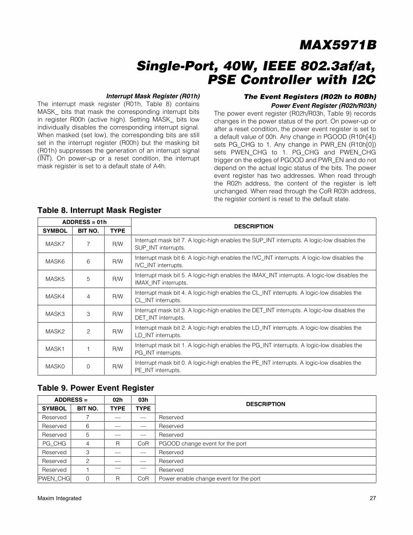
Interrupt Mask Register (R01h)The interrupt mask register (R01h, Table 8) contains MASK_ bits that mask the corresponding interrupt bits in register R00h (active high). Setting MASK_ bits low individually disables the corresponding interrupt signal. When masked (set low), the corresponding bits are still set in the interrupt register (R00h) but the masking bit (R01h) suppresses the generation of an interrupt signal (INT). On power-up or a reset condition, the interrupt mask register is set to a default state of A4h.
The Event Registers (R02h to R0Bh)Power Event Register (R02h/R03h)
The power event register (R02h/R03h, Table 9) records changes in the power status of the port. On power-up or after a reset condition, the power event register is set to a default value of 00h. Any change in PGOOD (R10h[4]) sets PG_CHG to 1. Any change in PWR_EN (R10h[0]) sets PWEN_CHG to 1. PG_CHG and PWEN_CHG trigger on the edges of PGOOD and PWR_EN and do not depend on the actual logic status of the bits. The power event register has two addresses. When read through the R02h address, the content of the register is left unchanged. When read through the CoR R03h address, the register content is reset to the default state.
Table 8. Interrupt Mask Register
Table 9. Power Event Register
ADDRESS = 01hDESCRIPTION
SYMBOL BIT NO. TYPE
MASK7 7 R/WInterrupt mask bit 7. A logic-high enables the SUP_INT interrupts. A logic-low disables the SUP_INT interrupts.
MASK6 6 R/WInterrupt mask bit 6. A logic-high enables the IVC_INT interrupts. A logic-low disables the IVC_INT interrupts.
MASK5 5 R/WInterrupt mask bit 5. A logic-high enables the IMAX_INT interrupts. A logic-low disables the IMAX_INT interrupts.
MASK4 4 R/WInterrupt mask bit 4. A logic-high enables the CL_INT interrupts. A logic-low disables the CL_INT interrupts.
MASK3 3 R/WInterrupt mask bit 3. A logic-high enables the DET_INT interrupts. A logic-low disables the DET_INT interrupts.
MASK2 2 R/WInterrupt mask bit 2. A logic-high enables the LD_INT interrupts. A logic-low disables the LD_INT interrupts.
MASK1 1 R/WInterrupt mask bit 1. A logic-high enables the PG_INT interrupts. A logic-low disables the PG_INT interrupts.
MASK0 0 R/WInterrupt mask bit 0. A logic-high enables the PE_INT interrupts. A logic-low disables the PE_INT interrupts.
ADDRESS = 02h 03hDESCRIPTION
SYMBOL BIT NO. TYPE TYPE
Reserved 7 — — Reserved
Reserved 6 — — Reserved
Reserved 5 — — Reserved
PG_CHG 4 R CoR PGOOD change event for the port
Reserved 3 — — Reserved
Reserved 2 — — Reserved
Reserved 1 — — Reserved
PWEN_CHG 0 R CoR Power enable change event for the port

28 Maxim Integrated
Single-Port, 40W, IEEE 802.3af/at, PSE Controller with I2C
MAX5971B
Detect Event Register (R04h/R05h)The detect event register (R04h/R05h, Table 10) records detection/classification events for the port. On power-up or after a reset condition, the detect event register is set to a default value of 00h. DET_END and CL_END are set high whenever detection/classification is completed. As with the other event registers, the detect event reg-ister has two addresses. When read through the R04h address, the content of the register is left unchanged. When read through the CoR R05h address, the register content is reset to the default state.
Fault Event Register (R06h/R07h)The fault event register (R06h/R07h, Table 11) records load removal and overcurrent events for the port. On power-up or after a reset condition, the fault event register is set to a default value of 00h. LD_DISC is set to 1 whenever the port shuts down due to detection of load removal. IMAX_FLT is set to 1 when the port shuts down due to an extended overcurrent event after a successful startup. As with the other events registers, the fault event reg-ister has two addresses. When read through the R06h address, the content of the register is left unchanged.
When read through the CoR R07h address, the register content is reset to the default state.
Startup Event Register (R08h/R09h)The startup event register (R08h/R09h, Table 12) records class overcurrent events for the port. On power-up or after a reset condition, the startup event register is set to a default value of 00h. IVC_FLT is set to 1 whenever a class overcurrent event occurs. The class overcurrent threshold used for the IVC_FLT bit is based upon the classification result. If automatic ICUT pro-gramming is used (default, Table 4) and ICUT is not manually reprogrammed (Tables 37 and 38), the IVC_FLT and IMAX_FLT (Table 11) flags are both set for any overcurrent event. Manually reprogramming the overcurrent threshold through ICUT settings does not affect the IVC_FLT flag thresholds, but does affect the IMAX_FLT thresholds. As with the other event registers, the startup event register has two addresses. When read through the R08h address, the content of the register is left unchanged. When read through the CoR R09h address, the register content is reset to the default state.
Table 10. Detect Event Register
Table 11. Fault Event Register
ADDRESS = 04h 05hDESCRIPTION
SYMBOL BIT NO. TYPE TYPE
Reserved 7 — — Reserved
Reserved 6 — — Reserved
Reserved 5 — — Reserved
CL_END 4 R CoR Classification completed on the port
Reserved 3 — — Reserved
Reserved 2 — — Reserved
Reserved 1 — — Reserved
DET_END 0 R CoR Detection completed on the port
ADDRESS = 06h 07hDESCRIPTION
SYMBOL BIT NO. TYPE TYPE
Reserved 7 — — Reserved
Reserved 6 — — Reserved
Reserved 5 — — Reserved
LD_DISC 4 R CoR Disconnect on the port
Reserved 3 — — Reserved
Reserved 2 — — Reserved
Reserved 1 — — Reserved
IMAX_FLT 0 R CoR Overcurrent on the port
29Maxim Integrated
Single-Port, 40W, IEEE 802.3af/at, PSE Controller with I2C
MAX5971B
Supply Event Register (R0Ah/R0Bh)The MAX5971B continuously monitors the power supplies and sets the appropriate bits in the supply event register (R0Ah/R0Bh, Table 13). On power-up or after a reset condition, the supply event register is set to a default value of 00h. VEE_OV is set to 1 whenever VEE exceeds its overvoltage threshold. VEE_UV is set to 1 whenever VEE falls below its undervoltage threshold.
A thermal shutdown circuit monitors the temperature of the die and resets the MAX5971B if the temperature exceeds +150NC. TSD is set to 1 after the MAX5971B returns to normal operation.
When VEE is below its UVLO threshold, the MAX5971B is in reset mode and securely holds the port off. When VEE rises above its UVLO threshold, the device comes out of reset and the VEE_UVLO bit in the supply event register is set to 1.
As with any of the other event registers, the supply event register has two addresses. When read through the R0Ah address, the content of the register is left unchanged. When read through the CoR R0Bh address, the register content is reset to the default state.
The Status Registers (R0Ch to R11h)Port Status Register (R0Ch)
The port status register (R0Ch, Table 14) records the results of the port detection and classification at the end of each phase in three encoded bits. On power-up or after a reset condition, the port status register is set to a
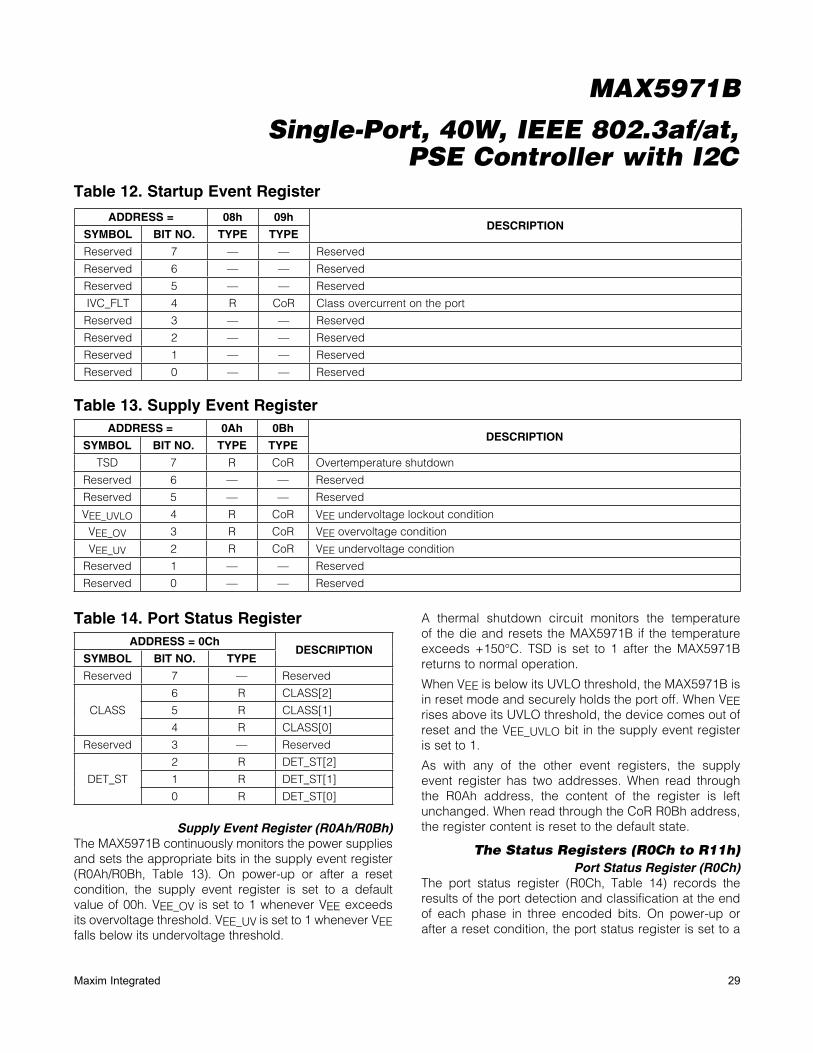
Table 13. Supply Event Register
Table 14. Port Status Register
Table 12. Startup Event Register
ADDRESS = 0Ah 0BhDESCRIPTION
SYMBOL BIT NO. TYPE TYPE
TSD 7 R CoR Overtemperature shutdown
Reserved 6 — — Reserved
Reserved 5 — — Reserved
VEE_UVLO 4 R CoR VEE undervoltage lockout condition
VEE_OV 3 R CoR VEE overvoltage condition
VEE_UV 2 R CoR VEE undervoltage condition
Reserved 1 — — Reserved
Reserved 0 — — Reserved
ADDRESS = 08h 09hDESCRIPTION
SYMBOL BIT NO. TYPE TYPE
Reserved 7 — — Reserved
Reserved 6 — — Reserved
Reserved 5 — — Reserved
IVC_FLT 4 R CoR Class overcurrent on the port
Reserved 3 — — Reserved
Reserved 2 — — Reserved
Reserved 1 — — Reserved
Reserved 0 — — Reserved
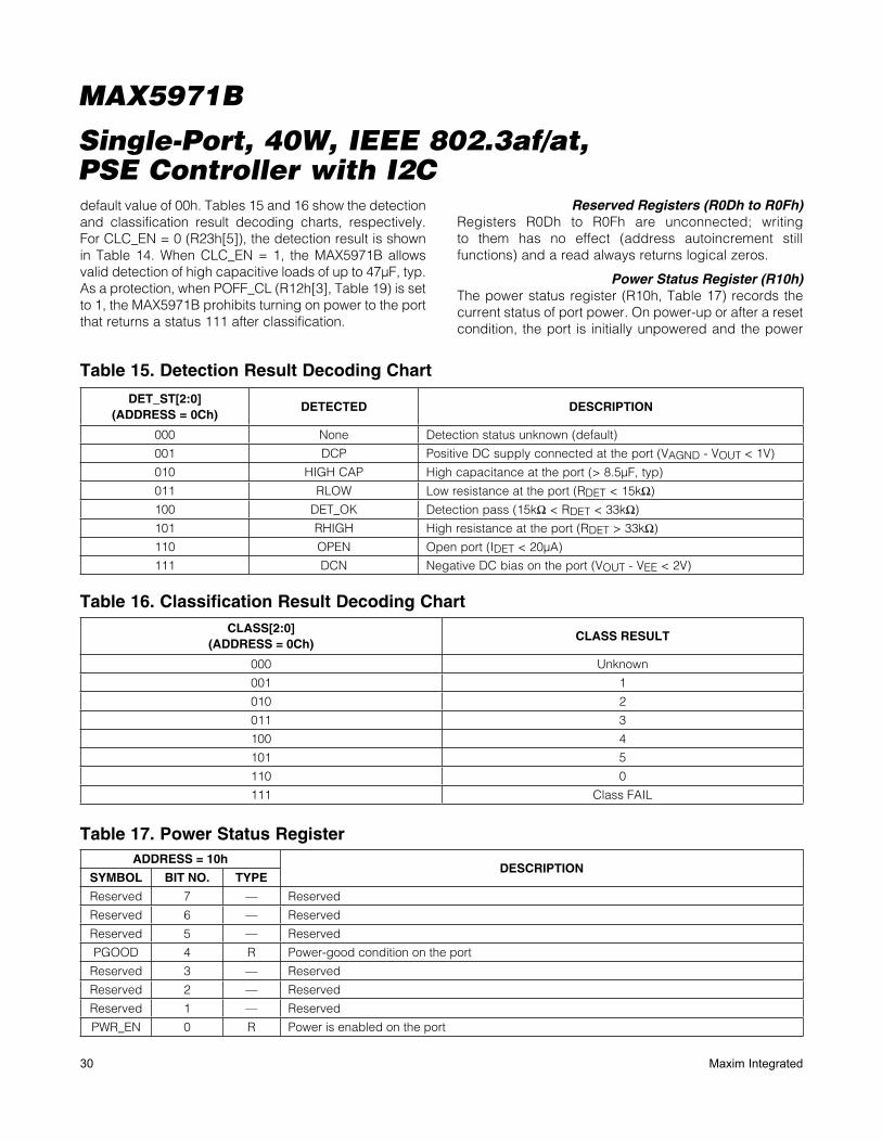
ADDRESS = 0ChDESCRIPTION
SYMBOL BIT NO. TYPE
Reserved 7 — Reserved
CLASS
6 R CLASS[2]
5 R CLASS[1]
4 R CLASS[0]
Reserved 3 — Reserved
DET_ST
2 R DET_ST[2]
1 R DET_ST[1]
0 R DET_ST[0]
30 Maxim Integrated
Single-Port, 40W, IEEE 802.3af/at, PSE Controller with I2C
MAX5971B
default value of 00h. Tables 15 and 16 show the detection and classification result decoding charts, respectively. For CLC_EN = 0 (R23h[5]), the detection result is shown in Table 14. When CLC_EN = 1, the MAX5971B allows valid detection of high capacitive loads of up to 47FF, typ. As a protection, when POFF_CL (R12h[3], Table 19) is set to 1, the MAX5971B prohibits turning on power to the port that returns a status 111 after classification.
Reserved Registers (R0Dh to R0Fh)Registers R0Dh to R0Fh are unconnected; writing to them has no effect (address autoincrement still functions) and a read always returns logical zeros.
Power Status Register (R10h)The power status register (R10h, Table 17) records the current status of port power. On power-up or after a reset condition, the port is initially unpowered and the power
Table 15. Detection Result Decoding Chart
Table 16. Classification Result Decoding Chart
Table 17. Power Status Register
DET_ST[2:0](ADDRESS = 0Ch)
DETECTED DESCRIPTION
000 None Detection status unknown (default)
001 DCP Positive DC supply connected at the port (VAGND - VOUT < 1V)
010 HIGH CAP High capacitance at the port (> 8.5FF, typ)
011 RLOW Low resistance at the port (RDET < 15kI)
100 DET_OK Detection pass (15kI < RDET < 33kI)
101 RHIGH High resistance at the port (RDET > 33kI)
110 OPEN Open port (IDET < 20FA)
111 DCN Negative DC bias on the port (VOUT - VEE < 2V)
CLASS[2:0](ADDRESS = 0Ch)
CLASS RESULT
000 Unknown
001 1
010 2
011 3
100 4
101 5
110 0
111 Class FAIL
ADDRESS = 10hDESCRIPTION
SYMBOL BIT NO. TYPE
Reserved 7 — Reserved
Reserved 6 — Reserved
Reserved 5 — Reserved
PGOOD 4 R Power-good condition on the port
Reserved 3 — Reserved
Reserved 2 — Reserved
Reserved 1 — Reserved
PWR_EN 0 R Power is enabled on the port
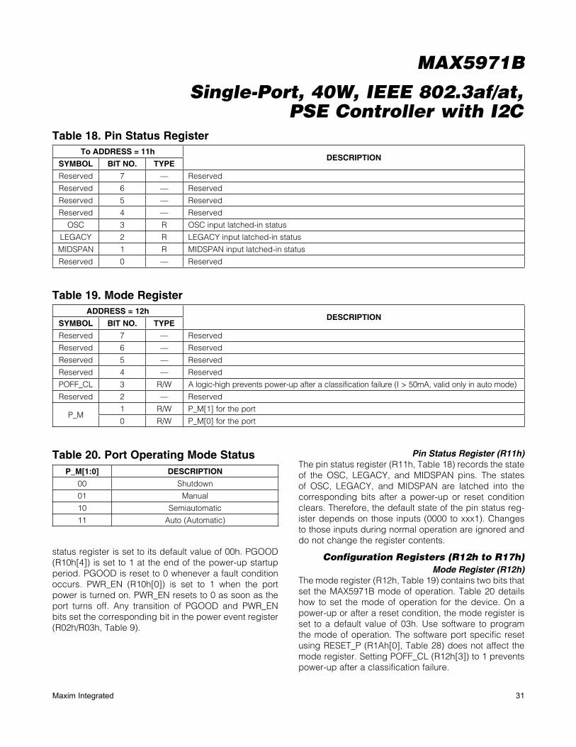
31Maxim Integrated
Single-Port, 40W, IEEE 802.3af/at, PSE Controller with I2C
MAX5971B
status register is set to its default value of 00h. PGOOD (R10h[4]) is set to 1 at the end of the power-up startup period. PGOOD is reset to 0 whenever a fault condition occurs. PWR_EN (R10h[0]) is set to 1 when the port power is turned on. PWR_EN resets to 0 as soon as the port turns off. Any transition of PGOOD and PWR_EN bits set the corresponding bit in the power event register (R02h/R03h, Table 9).
Pin Status Register (R11h)The pin status register (R11h, Table 18) records the state of the OSC, LEGACY, and MIDSPAN pins. The states of OSC, LEGACY, and MIDSPAN are latched into the corresponding bits after a power-up or reset condition clears. Therefore, the default state of the pin status reg-ister depends on those inputs (0000 to xxx1). Changes to those inputs during normal operation are ignored and do not change the register contents.
Configuration Registers (R12h to R17h)Mode Register (R12h)
The mode register (R12h, Table 19) contains two bits that set the MAX5971B mode of operation. Table 20 details how to set the mode of operation for the device. On a power-up or after a reset condition, the mode register is set to a default value of 03h. Use software to program the mode of operation. The software port specific reset using RESET_P (R1Ah[0], Table 28) does not affect the mode register. Setting POFF_CL (R12h[3]) to 1 prevents power-up after a classification failure.
Table 18. Pin Status Register
Table 19. Mode Register
Table 20. Port Operating Mode Status
To ADDRESS = 11hDESCRIPTION
SYMBOL BIT NO. TYPE
Reserved 7 — Reserved
Reserved 6 — Reserved
Reserved 5 — Reserved
Reserved 4 — Reserved
OSC 3 R OSC input latched-in status
LEGACY 2 R LEGACY input latched-in status
MIDSPAN 1 R MIDSPAN input latched-in status
Reserved 0 — Reserved
ADDRESS = 12hDESCRIPTION
SYMBOL BIT NO. TYPE
Reserved 7 — Reserved
Reserved 6 — Reserved
Reserved 5 — Reserved
Reserved 4 — Reserved
POFF_CL 3 R/W A logic-high prevents power-up after a classification failure (I > 50mA, valid only in auto mode)
Reserved 2 — Reserved
P_M1 R/W P_M[1] for the port
0 R/W P_M[0] for the port
P_M[1:0] DESCRIPTION
00 Shutdown
01 Manual
10 Semiautomatic
11 Auto (Automatic)
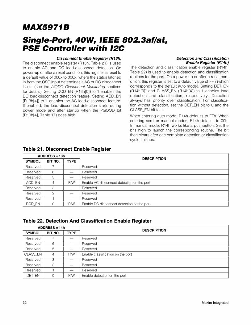
32 Maxim Integrated
Single-Port, 40W, IEEE 802.3af/at, PSE Controller with I2C
MAX5971B
Disconnect Enable Register (R13h)The disconnect enable register (R13h, Table 21) is used to enable AC and DC load-disconnect detection. On power-up or after a reset condition, this register is reset to a default value of 000x to 000x, where the status latched in from the OSC input determines if AC or DC disconnect is set (see the AC/DC Disconnect Monitoring sections for details). Setting DCD_EN (R13h[0]) to 1 enables the DC load-disconnect detection feature. Setting ACD_EN (R13h[4]) to 1 enables the AC load-disconnect feature. If enabled, the load-disconnect detection starts during power mode and after startup when the PGOOD bit (R10h[4], Table 17) goes high.
Detection and Classification Enable Register (R14h)
The detection and classification enable register (R14h, Table 22) is used to enable detection and classification routines for the port. On a power-up or after a reset con-dition, this register is set to a default value of FFh (which corresponds to the default auto mode). Setting DET_EN (R14h[0]) and CLASS_EN (R14h[4]) to 1 enables load detection and classification, respectively. Detection always has priority over classification. For classifica-tion without detection, set the DET_EN bit to 0 and the CLASS_EN bit to 1.
When entering auto mode, R14h defaults to FFh. When entering semi or manual modes, R14h defaults to 00h. In manual mode, R14h works like a pushbutton. Set the bits high to launch the corresponding routine. The bit then clears after one complete detection or classification cycle finishes.
Table 21. Disconnect Enable Register
Table 22. Detection And Classification Enable Register
ADDRESS = 13hDESCRIPTION
SYMBOL BIT NO. TYPE
Reserved 7 — Reserved
Reserved 6 — Reserved
Reserved 5 — Reserved
ACD_EN 4 R/W Enable AC disconnect detection on the port
Reserved 3 — Reserved
Reserved 2 — Reserved
Reserved 1 — Reserved
DCD_EN 0 R/W Enable DC disconnect detection on the port
ADDRESS = 14hDESCRIPTION
SYMBOL BIT NO. TYPE
Reserved 7 — Reserved
Reserved 6 — Reserved
Reserved 5 — Reserved
CLASS_EN 4 R/W Enable classification on the port
Reserved 3 — Reserved
Reserved 2 — Reserved
Reserved 1 — Reserved
DET_EN 0 R/W Enable detection on the port
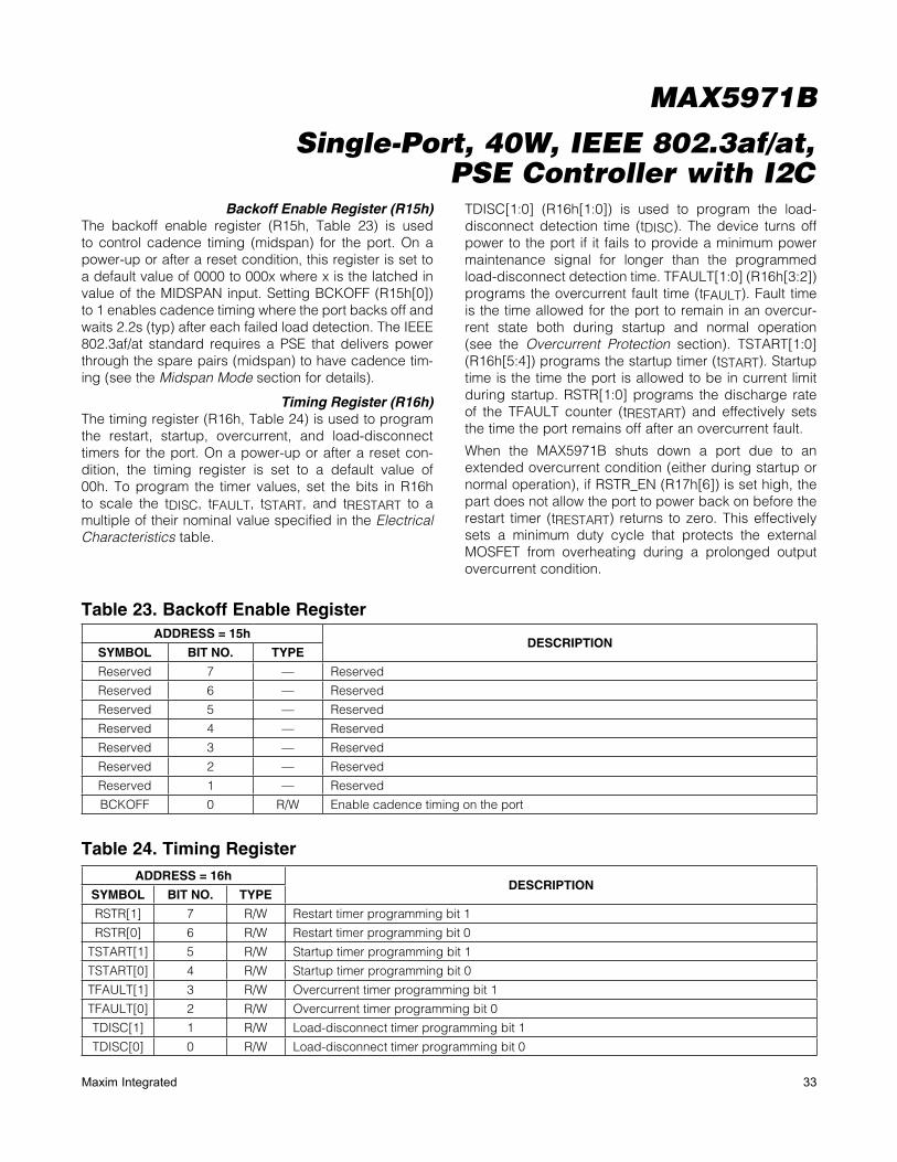
33Maxim Integrated
Single-Port, 40W, IEEE 802.3af/at, PSE Controller with I2C
MAX5971B
Backoff Enable Register (R15h)The backoff enable register (R15h, Table 23) is used to control cadence timing (midspan) for the port. On a power-up or after a reset condition, this register is set to a default value of 0000 to 000x where x is the latched in value of the MIDSPAN input. Setting BCKOFF (R15h[0]) to 1 enables cadence timing where the port backs off and waits 2.2s (typ) after each failed load detection. The IEEE 802.3af/at standard requires a PSE that delivers power through the spare pairs (midspan) to have cadence tim-ing (see the Midspan Mode section for details).
Timing Register (R16h)The timing register (R16h, Table 24) is used to program the restart, startup, overcurrent, and load-disconnect timers for the port. On a power-up or after a reset con-dition, the timing register is set to a default value of 00h. To program the timer values, set the bits in R16h to scale the tDISC, tFAULT, tSTART, and tRESTART to a multiple of their nominal value specified in the Electrical Characteristics table.
TDISC[1:0] (R16h[1:0]) is used to program the load-disconnect detection time (tDISC). The device turns off power to the port if it fails to provide a minimum power maintenance signal for longer than the programmed load-disconnect detection time. TFAULT[1:0] (R16h[3:2]) programs the overcurrent fault time (tFAULT). Fault time is the time allowed for the port to remain in an overcur-rent state both during startup and normal operation (see the Overcurrent Protection section). TSTART[1:0] (R16h[5:4]) programs the startup timer (tSTART). Startup time is the time the port is allowed to be in current limit during startup. RSTR[1:0] programs the discharge rate of the TFAULT counter (tRESTART) and effectively sets the time the port remains off after an overcurrent fault.
When the MAX5971B shuts down a port due to an extended overcurrent condition (either during startup or normal operation), if RSTR_EN (R17h[6]) is set high, the part does not allow the port to power back on before the restart timer (tRESTART) returns to zero. This effectively sets a minimum duty cycle that protects the external MOSFET from overheating during a prolonged output overcurrent condition.
Table 23. Backoff Enable Register
Table 24. Timing Register
ADDRESS = 15hDESCRIPTION
SYMBOL BIT NO. TYPE
Reserved 7 — Reserved
Reserved 6 — Reserved
Reserved 5 — Reserved
Reserved 4 — Reserved
Reserved 3 — Reserved
Reserved 2 — Reserved
Reserved 1 — Reserved
BCKOFF 0 R/W Enable cadence timing on the port
ADDRESS = 16hDESCRIPTION
SYMBOL BIT NO. TYPE
RSTR[1] 7 R/W Restart timer programming bit 1
RSTR[0] 6 R/W Restart timer programming bit 0
TSTART[1] 5 R/W Startup timer programming bit 1
TSTART[0] 4 R/W Startup timer programming bit 0
TFAULT[1] 3 R/W Overcurrent timer programming bit 1
TFAULT[0] 2 R/W Overcurrent timer programming bit 0
TDISC[1] 1 R/W Load-disconnect timer programming bit 1
TDISC[0] 0 R/W Load-disconnect timer programming bit 0
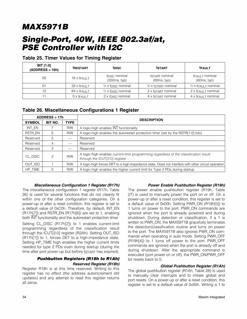
34 Maxim Integrated
Single-Port, 40W, IEEE 802.3af/at, PSE Controller with I2C
MAX5971B
Miscellaneous Configuration 1 Register (R17h)The miscellaneous configuration 1 register (R17h, Table 26) is used for several functions that do not cleanly fit within one of the other configuration categories. On a power-up or after a reset condition, this register is set to a default value of 0xC0h. Therefore, by default, INT_EN (R17h[7]) and RSTR_EN (R17h[6]) are set to 1, enabling both INT functionality and the autorestart protection timer.
Setting CL_DISC (R17h[2]) to 1 enables current-limit programming regardless of the classification result through the ICUT[2:0] register (R2Ah). Setting OUT_ISO (R17h[1]) to 1, forces DET to a high-impedance state. Setting HP_TIME high enables the higher current limits needed for type 2 PDs even during startup (during the time after port power-up but before tSTART has expired).
Pushbutton Registers (R18h to R1Ah)Reserved Register (R18h)
Register R18h is at this time reserved. Writing to this register has no effect (the address autoincrement still updates) and any attempt to read this register returns all zeros.
Power Enable Pushbutton Register (R19h)The power enable pushbutton register (R19h, Table 27) is used to manually power the port on or off. On a power-up or after a reset condition, this register is set to a default value of 0x00h. Setting PWR_ON (R19h[0]) to 1 turns on power to the port. PWR_ON commands are ignored when the port is already powered and during shutdown. During detection or classification, if a 1 is written to PWR_ON, the MAX5971B gracefully terminates the detection/classification routine and turns on power to the port. The MAX5971B also ignores PWR_ON com-mands when operating in auto mode. Setting PWR_OFF (R19h[4]) to 1 turns off power to the port. PWR_OFF commands are ignored when the port is already off and during shutdown. After the appropriate command is executed (port power on or off), the PWR_ON/PWR_OFF bit resets back to 0.
Global Pushbutton Register (R1Ah)The global pushbutton register (R1Ah, Table 28) is used to manually clear interrupts and to initiate global and port resets. On a power-up or after a reset condition, this register is set to a default value of 0x00h. Writing a 1 to
Table 25. Timer Values for Timing Register
Table 26. Miscellaneous Configurations 1 Register
BIT [1:0](ADDRESS = 16h)
tRESTART tDISC tSTART tFAULT
00 16 x tFAULTtDISC nominal(350ms, typ)
tSTART nominal(60ms, typ)
tFAULT nominal(60ms, typ)
01 32 x tFAULT ¼ x tDISC nominal ½ x tSTART nominal ½ x tFAULT nominal
10 64 x tFAULT ½ x tDISC nominal 2 x tSTART nominal 2 x tFAULT nominal
11 0 x tFAULT 2 x tDISC nominal 4 x tSTART nominal 4 x tFAULT nominal
ADDRESS = 17hDESCRIPTION
SYMBOL BIT NO. TYPE
INT_EN 7 R/W A logic-high enables INT functionalityRSTR_EN 6 R/W A logic-high enables the autorestart protection timer (set by the RSTR[1:0] bits)
Reserved 5 — Reserved
Reserved 4 — Reserved
Reserved 3 — Reserved
CL_DISC 2 R/WA logic-high enables current-limit programming regardless of the classification result through the ICUT[2:0] register
OUT_ISO 1 R/W A logic-high forces DET to a high-impedance state. Does not interfere with other circuit operation.
HP_TIME 0 R/W A logic-high enables the higher current limit for Type 2 PDs during startup.
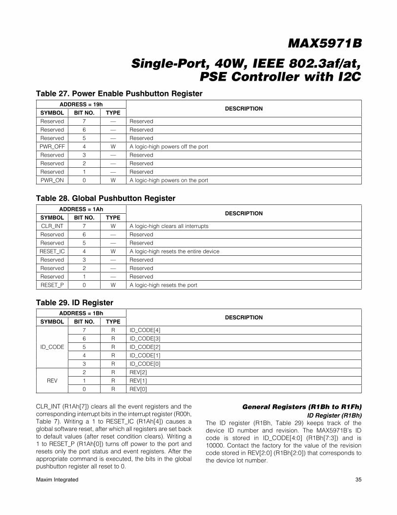
35Maxim Integrated
Single-Port, 40W, IEEE 802.3af/at, PSE Controller with I2C
MAX5971B
CLR_INT (R1Ah[7]) clears all the event registers and the corresponding interrupt bits in the interrupt register (R00h, Table 7). Writing a 1 to RESET_IC (R1Ah[4]) causes a global software reset, after which all registers are set back to default values (after reset condition clears). Writing a 1 to RESET_P (R1Ah[0]) turns off power to the port and resets only the port status and event registers. After the appropriate command is executed, the bits in the global pushbutton register all reset to 0.
General Registers (R1Bh to R1Fh)ID Register (R1Bh)
The ID register (R1Bh, Table 29) keeps track of the device ID number and revision. The MAX5971B’s ID code is stored in ID_CODE[4:0] (R1Bh[7:3]) and is 10000. Contact the factory for the value of the revision code stored in REV[2:0] (R1Bh[2:0]) that corresponds to the device lot number.
Table 27. Power Enable Pushbutton Register
Table 28. Global Pushbutton Register
Table 29. ID Register
ADDRESS = 19hDESCRIPTION
SYMBOL BIT NO. TYPE
Reserved 7 — Reserved
Reserved 6 — Reserved
Reserved 5 — Reserved
PWR_OFF 4 W A logic-high powers off the port
Reserved 3 — Reserved
Reserved 2 — Reserved
Reserved 1 — Reserved
PWR_ON 0 W A logic-high powers on the port
ADDRESS = 1AhDESCRIPTION
SYMBOL BIT NO. TYPE
CLR_INT 7 W A logic-high clears all interrupts
Reserved 6 — Reserved
Reserved 5 — Reserved
RESET_IC 4 W A logic-high resets the entire device
Reserved 3 — Reserved
Reserved 2 — Reserved
Reserved 1 — Reserved
RESET_P 0 W A logic-high resets the port
ADDRESS = 1BhDESCRIPTION
SYMBOL BIT NO. TYPE
ID_CODE
7 R ID_CODE[4]
6 R ID_CODE[3]
5 R ID_CODE[2]
4 R ID_CODE[1]
3 R ID_CODE[0]
REV
2 R REV[2]
1 R REV[1]
0 R REV[0]
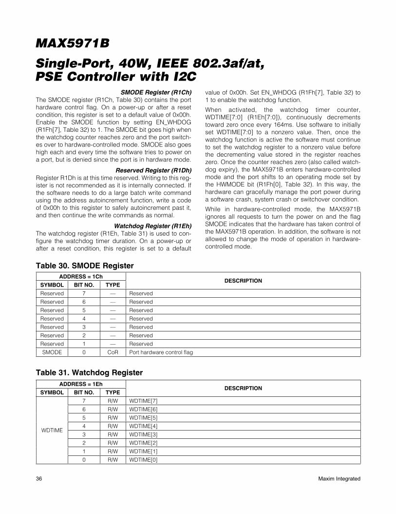
36 Maxim Integrated
Single-Port, 40W, IEEE 802.3af/at, PSE Controller with I2C
MAX5971B
SMODE Register (R1Ch)The SMODE register (R1Ch, Table 30) contains the port hardware control flag. On a power-up or after a reset condition, this register is set to a default value of 0x00h. Enable the SMODE function by setting EN_WHDOG (R1Fh[7], Table 32) to 1. The SMODE bit goes high when the watchdog counter reaches zero and the port switch-es over to hardware-controlled mode. SMODE also goes high each and every time the software tries to power on a port, but is denied since the port is in hardware mode.
Reserved Register (R1Dh)Register R1Dh is at this time reserved. Writing to this reg-ister is not recommended as it is internally connected. If the software needs to do a large batch write command using the address autoincrement function, write a code of 0x00h to this register to safely autoincrement past it, and then continue the write commands as normal.
Watchdog Register (R1Eh)The watchdog register (R1Eh, Table 31) is used to con-figure the watchdog timer duration. On a power-up or after a reset condition, this register is set to a default
value of 0x00h. Set EN_WHDOG (R1Fh[7], Table 32) to 1 to enable the watchdog function.
When activated, the watchdog timer counter, WDTIME[7:0] (R1Eh[7:0]), continuously decrements toward zero once every 164ms. Use software to initially set WDTIME[7:0] to a nonzero value. Then, once the watchdog function is active the software must continue to set the watchdog register to a nonzero value before the decrementing value stored in the register reaches zero. Once the counter reaches zero (also called watch-dog expiry), the MAX5971B enters hardware-controlled mode and the port shifts to an operating mode set by the HWMODE bit (R1Fh[0], Table 32). In this way, the hardware can gracefully manage the port power during a software crash, system crash or switchover condition.
While in hardware-controlled mode, the MAX5971B ignores all requests to turn the power on and the flag SMODE indicates that the hardware has taken control of the MAX5971B operation. In addition, the software is not allowed to change the mode of operation in hardware-controlled mode.
Table 30. SMODE Register
Table 31. Watchdog Register
ADDRESS = 1ChDESCRIPTION
SYMBOL BIT NO. TYPE
Reserved 7 — Reserved
Reserved 6 — Reserved
Reserved 5 — Reserved
Reserved 4 — Reserved
Reserved 3 — Reserved
Reserved 2 — Reserved
Reserved 1 — Reserved
SMODE 0 CoR Port hardware control flag
ADDRESS = 1EhDESCRIPTION
SYMBOL BIT NO. TYPE
WDTIME
7 R/W WDTIME[7]
6 R/W WDTIME[6]
5 R/W WDTIME[5]
4 R/W WDTIME[4]
3 R/W WDTIME[3]
2 R/W WDTIME[2]
1 R/W WDTIME[1]
0 R/W WDTIME[0]

37Maxim Integrated
Single-Port, 40W, IEEE 802.3af/at, PSE Controller with I2C
MAX5971B
Switch Mode Register (R1Fh)The switch mode register (R1Fh, Table 32) is used to enable the watchdog timer, interrupt, and watchdog expiry port state. On a power-up or after a reset condi-tion, this register is set to a default value of 0x00h.
Set EN_WHDOG (R1Fh[7], Table 32) to 1 to enable the watchdog function. When the watchdog counter reaches zero, the hardware-controlled mode activates and sets the port to the operating mode determined by the HWMODE bit (R1Fh[0]). A 0 in HWMODE places the port into shutdown mode by setting the P_M[1:0] bits (R12h[1:0]) to 00. A 1 in HWMODE places the port into auto mode by setting the P_M[1:0] bits to 11. If WD_INT_EN is set to 1, an interrupt is sent if the SMODE bit is set.
Special and Reserved Registers (R20h to R2Fh)
Reserved Registers (R20h to R22h, R25h to R28h, and R2Bh to R2Fh)
These registers are reserved. Writing to these registers is not recommended as they are internally connected. If
the software needs to do a large batch write command using the address autoincrement function, write a code of 0x00h to these registers to safely autoincrement past them, and then continue the write commands as normal.
Program Register (R23h)The program register (R23h, Table 33) is used to enable large capacitor detection, skipping detection in AUTO mode and for setting the AC disconnect threshold. On a power-up or after a reset condition, this register is set to a default value of 00x0 to 0100.
CLC_EN (R23h[5]) enables the large capacitor detec-tion feature. The CLC_EN register can be programmed directly by the software or by using the LEGACY input (see the High Capacitance Detection section). When CLC_EN = 1 the device can recognize a capacitor load up to 47FF, typ. If the CLC_EN = 0, the MAX5971B per-forms normal detection.
DET_BY (R23h[4]) is used to allow the port to power when skipping the detection routine in auto mode. When DET_BY is set to 0 (default), the port cannot power up if the port detection sequence was bypassed in auto
Table 32. Switch Mode Register
Table 33. Program Register
ADDRESS = 1FhDESCRIPTION
SYMBOL BIT NO. TYPE
EN_WHDOG 7 R/W A logic-high enables the watchdog function
WD_INT_EN 6 R/W Enables interrupt on SMODE bit
Reserved 5 — Reserved
Reserved 4 — Reserved
Reserved 3 — Reserved
Reserved 2 — Reserved
Reserved 1 — Reserved
HWMODE 0 R/WPort switches to auto mode if logic-high and to shutdown mode if logic-low when watchdog timer expires
ADDRESS = 23hDESCRIPTION
SYMBOL BIT NO. TYPE
Reserved7 R/W
Internally connected. For a write command, always write a zero to this bit.6 R/W
CLC_EN 5 R/W Large capacitor detection enable
DET_BY 4 R/W Enables skipping detection in auto mode
Reserved 3 — Reserved
AC_TH
2 R/W AC_TH[2]
1 R/W AC_TH[1]
0 R/W AC_TH[0]

38 Maxim Integrated
Single-Port, 40W, IEEE 802.3af/at, PSE Controller with I2C
MAX5971B
mode. When DET_BY is set to 1 however, the MAX5971B can power the port without doing the detection routine.
AC_TH[2:0] (R23h[2:0]) allows direct programming of the AC disconnect threshold. The threshold is defined as a current since the comparator verifies that the peak current pulses sensed at the DET input exceeds a preset threshold. The current threshold is defined as follows:
IAC_TH = 85.28FA + 10.64FA x NAC_TH
where NAC_TH is the decimal value of AC_TH[2:0]. The default NAC_TH is 4 (AC_TH[2:0] = 100) which corresponds to a default IAC_TH of ~128FA.
PWM Register (R24h)The PWM register (R24h, Table 34) is used to program the PWM duty cycle. On a power-up or after a reset condition, this register is set to a default value of 0x00h. PWM_TH[1:0] (R24h[5:4]) is used to set the PWM duty cycle. The default PWM_TH[1:0] value of 00 corresponds to a 6.25% duty cycle, while the maximum PWM_TH[1:0] value of 11 corresponds to a 25% duty cycle (see Table 35).
Table 34. PWM Register
Table 35. PWM Duty-Cycle Settings
ADDRESS = 24hDESCRIPTION
SYMBOL BIT NO. TYPE
Reserved 7 — Reserved
Reserved 6 — Reserved
PWM_TH5 R/W PWM_TH[1]
4 R/W PWM_TH[0]
Reserved
3 R/W
Internally connected. For a write command, always write a zero to this bit.2 R/W
1 R/W
0 R/W
PWM_TH[1:0] DUTY CYCLE (%)
00 6.25
01 12.5
10 18.75
11 25.0
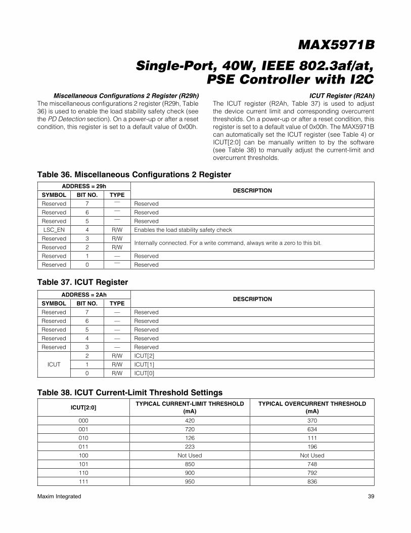
39Maxim Integrated
Single-Port, 40W, IEEE 802.3af/at, PSE Controller with I2C
MAX5971B
Table 37. ICUT Register
Table 38. ICUT Current-Limit Threshold Settings
Table 36. Miscellaneous Configurations 2 Register
Miscellaneous Configurations 2 Register (R29h)The miscellaneous configurations 2 register (R29h, Table 36) is used to enable the load stability safety check (see the PD Detection section). On a power-up or after a reset condition, this register is set to a default value of 0x00h.
ICUT Register (R2Ah)The ICUT register (R2Ah, Table 37) is used to adjust the device current limit and corresponding overcurrent thresholds. On a power-up or after a reset condition, this register is set to a default value of 0x00h. The MAX5971B can automatically set the ICUT register (see Table 4) or ICUT[2:0] can be manually written to by the software (see Table 38) to manually adjust the current-limit and overcurrent thresholds.
ADDRESS = 29hDESCRIPTION
SYMBOL BIT NO. TYPE
Reserved 7 — Reserved
Reserved 6 — Reserved
Reserved 5 — Reserved
LSC_EN 4 R/W Enables the load stability safety check
Reserved 3 R/WInternally connected. For a write command, always write a zero to this bit.
Reserved 2 R/W
Reserved 1 — Reserved
Reserved 0 — Reserved
ADDRESS = 2AhDESCRIPTION
SYMBOL BIT NO. TYPE
Reserved 7 — Reserved
Reserved 6 — Reserved
Reserved 5 — Reserved
Reserved 4 — Reserved
Reserved 3 — Reserved
ICUT
2 R/W ICUT[2]
1 R/W ICUT[1]
0 R/W ICUT[0]
ICUT[2:0]TYPICAL CURRENT-LIMIT THRESHOLD
(mA)TYPICAL OVERCURRENT THRESHOLD
(mA)
000 420 370
001 720 634
010 126 111
011 223 196
100 Not Used Not Used
101 850 748
110 900 792
111 950 836
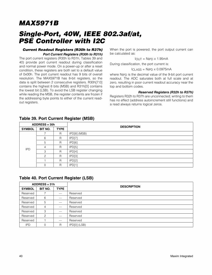
40 Maxim Integrated
Single-Port, 40W, IEEE 802.3af/at, PSE Controller with I2C
MAX5971B
Current Readout Registers (R30h to R37h)Port Current Registers (R30h to R31h)
The port current registers (R30h to R31h, Tables 39 and 40) provide port current readout during classification and normal power mode. On a power-up or after a reset condition, these registers are both set to a default value of 0x00h. The port current readout has 9 bits of overall resolution. The MAX5971B has 8-bit registers, so the data is split between 2 consecutive registers. R30h[7:0] contains the highest 8 bits (MSB) and R31h[0] contains the lowest bit (LSB). To avoid the LSB register changing while reading the MSB, the register contents are frozen if the addressing byte points to either of the current read-out registers.
When the port is powered, the port output current can be calculated as:
IOUT = NIPD x 1.95mA
During classification, the port current is:
ICLASS = NIPD x 0.0975mA
where NIPD is the decimal value of the 9-bit port current readout. The ADC saturates both at full scale and at zero, resulting in poor current readout accuracy near the top and bottom codes.
Reserved Registers (R32h to R37h)Registers R32h to R37h are unconnected; writing to them has no effect (address autoincrement still functions) and a read always returns logical zeros.
Table 39. Port Current Register (MSB)
Table 40. Port Current Register (LSB)
ADDRESS = 30hDESCRIPTION
SYMBOL BIT NO. TYPE
IPD
7 R IPD[8] (MSB)
6 R IPD[7]
5 R IPD[6]
4 R IPD[5]
3 R IPD[4]
2 R IPD[3]
1 R IPD[2]
0 R IPD[1]
ADDRESS = 31hDESCRIPTION
SYMBOL BIT NO. TYPE
Reserved 7 — Reserved
Reserved 6 — Reserved
Reserved 5 — Reserved
Reserved 4 — Reserved
Reserved 3 — Reserved
Reserved 2 — Reserved
Reserved 1 — Reserved
IPD 0 R IPD[0] (LSB)
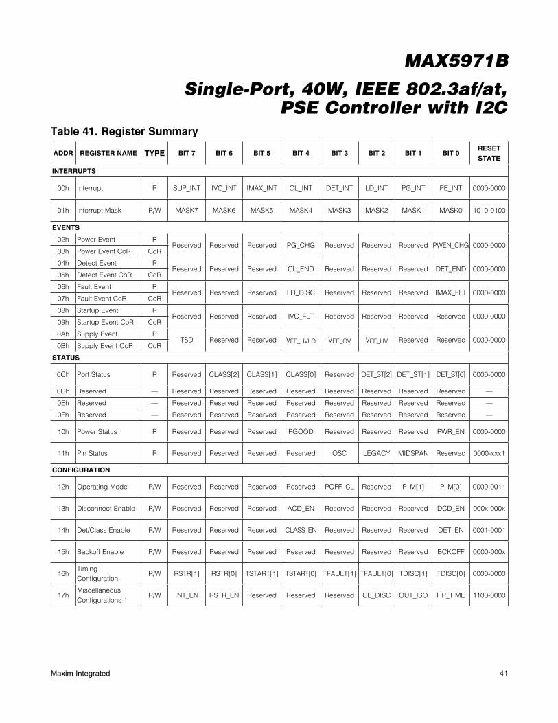
41Maxim Integrated
Single-Port, 40W, IEEE 802.3af/at, PSE Controller with I2C
MAX5971B
Table 41. Register Summary
ADDR REGISTER NAME TYPE BIT 7 BIT 6 BIT 5 BIT 4 BIT 3 BIT 2 BIT 1 BIT 0RESET STATE
INTERRUPTS
00h Interrupt R SUP_INT IVC_INT IMAX_INT CL_INT DET_INT LD_INT PG_INT PE_INT 0000-0000
01h Interrupt Mask R/W MASK7 MASK6 MASK5 MASK4 MASK3 MASK2 MASK1 MASK0 1010-0100
EVENTS
02h Power Event RReserved Reserved Reserved PG_CHG Reserved Reserved Reserved PWEN_CHG 0000-0000
03h Power Event CoR CoR
04h Detect Event RReserved Reserved Reserved CL_END Reserved Reserved Reserved DET_END 0000-0000
05h Detect Event CoR CoR
06h Fault Event RReserved Reserved Reserved LD_DISC Reserved Reserved Reserved IMAX_FLT 0000-0000
07h Fault Event CoR CoR
08h Startup Event RReserved Reserved Reserved IVC_FLT Reserved Reserved Reserved Reserved 0000-0000
09h Startup Event CoR CoR
0Ah Supply Event RTSD Reserved Reserved VEE_UVLO VEE_OV VEE_UV Reserved Reserved 0000-0000
0Bh Supply Event CoR CoR
STATUS
0Ch Port Status R Reserved CLASS[2] CLASS[1] CLASS[0] Reserved DET_ST[2] DET_ST[1] DET_ST[0] 0000-0000
0Dh Reserved — Reserved Reserved Reserved Reserved Reserved Reserved Reserved Reserved —
0Eh Reserved — Reserved Reserved Reserved Reserved Reserved Reserved Reserved Reserved —
0Fh Reserved — Reserved Reserved Reserved Reserved Reserved Reserved Reserved Reserved —
10h Power Status R Reserved Reserved Reserved PGOOD Reserved Reserved Reserved PWR_EN 0000-0000
11h Pin Status R Reserved Reserved Reserved Reserved OSC LEGACY MIDSPAN Reserved 0000-xxx1
CONFIGURATION
12h Operating Mode R/W Reserved Reserved Reserved Reserved POFF_CL Reserved P_M[1] P_M[0] 0000-0011
13h Disconnect Enable R/W Reserved Reserved Reserved ACD_EN Reserved Reserved Reserved DCD_EN 000x-000x
14h Det/Class Enable R/W Reserved Reserved Reserved CLASS_EN Reserved Reserved Reserved DET_EN 0001-0001
15h Backoff Enable R/W Reserved Reserved Reserved Reserved Reserved Reserved Reserved BCKOFF 0000-000x
16hTiming Configuration
R/W RSTR[1] RSTR[0] TSTART[1] TSTART[0] TFAULT[1] TFAULT[0] TDISC[1] TDISC[0] 0000-0000
17hMiscellaneous Configurations 1
R/W INT_EN RSTR_EN Reserved Reserved Reserved CL_DISC OUT_ISO HP_TIME 1100-0000

42 Maxim Integrated
Single-Port, 40W, IEEE 802.3af/at, PSE Controller with I2C
MAX5971B
Table 41. Register Summary (continued)
ADDR REGISTER NAME TYPE BIT 7 BIT 6 BIT 5 BIT 4 BIT 3 BIT 2 BIT 1 BIT 0RESET STATE
PUSHBUTTONS
18h Reserved — Reserved Reserved Reserved Reserved Reserved Reserved Reserved Reserved —
19h Power Enable W Reserved Reserved Reserved PWR_OFF Reserved Reserved Reserved PWR_ON 0000-0000
1Ah Global W CLR_INT Reserved Reserved RESET_IC Reserved Reserved Reserved RESET_P 0000-0000
GENERAL
1Bh ID R ID_CODE[4] ID_CODE[3] ID_CODE[2] ID_CODE[1] ID_CODE[0] REV[2] REV[1] REV[0] 1000-0xxx
1Ch SMODE CoR Reserved Reserved Reserved Reserved Reserved Reserved Reserved SMODE 0000-0000
1Dh Reserved — Reserved Reserved Reserved Reserved Reserved Reserved Reserved Reserved —
1Eh Watchdog R/W WDTIME[7] WDTIME[6] WDTIME[5] WDTIME[4] WDTIME[3] WDTIME[2] WDTIME[1] WDTIME[0] 0000-0000
1Fh Switch Mode R/W EN_WHDOG WD_INT_EN Reserved Reserved Reserved Reserved Reserved HWMODE 0000-0000
SPECIAL/RESERVED
20h Reserved — Reserved Reserved Reserved Reserved Reserved Reserved Reserved Reserved —
21h Reserved — Reserved Reserved Reserved Reserved Reserved Reserved Reserved Reserved —
22h Reserved — Reserved Reserved Reserved Reserved Reserved Reserved Reserved Reserved —
23h Program R/W Reserved Reserved CLC_EN DET_BY Reserved AC_TH[2] AC_TH[1] AC_TH[0] 00x0-0100
24h PWM R/W Reserved Reserved PWM_TH[1] PWM_TH[0] Reserved Reserved Reserved Reserved 0000-0000
25h Reserved — Reserved Reserved Reserved Reserved Reserved Reserved Reserved Reserved —
26h Reserved — Reserved Reserved Reserved Reserved Reserved Reserved Reserved Reserved —
27h Reserved — Reserved Reserved Reserved Reserved Reserved Reserved Reserved Reserved —
28h Reserved — Reserved Reserved Reserved Reserved Reserved Reserved Reserved Reserved —
29hMiscellaneous Configurations 2
R/W Reserved Reserved Reserved LSC_EN Reserved Reserved Reserved Reserved 0000-0000
2Ah ICUT R/W Reserved Reserved Reserved Reserved Reserved ICUT[2] ICUT[1] ICUT[0] 0000-0000
2Bh Reserved — Reserved Reserved Reserved Reserved Reserved Reserved Reserved Reserved —
2Ch Reserved — Reserved Reserved Reserved Reserved Reserved Reserved Reserved Reserved —
2Dh Reserved — Reserved Reserved Reserved Reserved Reserved Reserved Reserved Reserved —
2Eh Reserved — Reserved Reserved Reserved Reserved Reserved Reserved Reserved Reserved —
2Fh Reserved — Reserved Reserved Reserved Reserved Reserved Reserved Reserved Reserved —

43Maxim Integrated
Single-Port, 40W, IEEE 802.3af/at, PSE Controller with I2C
MAX5971B
Applications InformationLayout Procedure
Careful PCB layout is critical to achieve high efficiency and low EMI. Follow these layout guidelines for optimal performance.
1) Place the high-frequency input bypass capacitor (0.1FF ceramic capacitor from AGND to VEE) and the output bypass capacitor (0.1FF ceramic capacitor from AGND to OUTP) as close as possible to the MAX5971B.
2) Use large SMT component pads for power dissipat-ing devices, such as the MAX5971B and the external diodes in the high-power path.
3) Use short, wide traces whenever possible for high- power paths.
4) Use the MAX5971B Evaluation Kit as a design and layout reference.
5) The EP must be soldered evenly to the PCB ground plane (VEE) for proper operation and power dissipa-tion. Use multiple vias beneath the EP for maximum heat dissipation. A 1.0mm to 1.2mm pitch is the recommended spacing for these vias and should be plated (1oz copper) with a small barrel diameter (0.30mm to 0.33mm).
Figure 15. Typical Operating Circuit 1 (DC Load Removal Detection, Internal PWM Enabled for LED Indication, and Class 5 Detection Enabled)
Table 41. Register Summary (continued)
5.1kI
1kI
1kI
2.2MI0.1µF100VSMJ58A
-54V
-54V
47µF100V
0.1µF100V
1N4448
1N4448
10mH
1nF
AGND
SERIAL INTERFACE
SDA SCL AD0 INT
VEE
VEE_DIG
EN
LED
LED
LEGACYMIDSPANOSC
OUT
OUTP
PWMEN
DET
ILIM1
ILIM2
MAX5971B
PSE OUTPUT
ADDR REGISTER NAME TYPE BIT 7 BIT 6 BIT 5 BIT 4 BIT 3 BIT 2 BIT 1 BIT 0RESET STATE
CURRENT READOUT
30h Port Current (MSB) R IPD[8] IPD[7] IPD[6] IPD[5] IPD[4] IPD[3] IPD[2] IPD[1] 0000-0000
31h Port Current (LSB) R Reserved Reserved Reserved Reserved Reserved Reserved Reserved IPD[0] 0000-0000
32h Reserved — Reserved Reserved Reserved Reserved Reserved Reserved Reserved Reserved —
33h Reserved — Reserved Reserved Reserved Reserved Reserved Reserved Reserved Reserved —
34h Reserved — Reserved Reserved Reserved Reserved Reserved Reserved Reserved Reserved —
35h Reserved — Reserved Reserved Reserved Reserved Reserved Reserved Reserved Reserved —
36h Reserved — Reserved Reserved Reserved Reserved Reserved Reserved Reserved Reserved —
37h Reserved — Reserved Reserved Reserved Reserved Reserved Reserved Reserved Reserved —

44 Maxim Integrated
Single-Port, 40W, IEEE 802.3af/at, PSE Controller with I2C
MAX5971B
Figure 17. Typical Operating Circuit 3 (IEEE 802.3at Compliant, Minimal Application Circuit with DC Load Removal Detection and No LED Indication)
Figure 16. Typical Operating Circuit 2 (AC Load Removal Detection, Internal PWM Enabled for LED Indication, and Class 5 Detection Enabled)
-54V AGND
SDA SCL AD0 INT
LED
PWMEN
VEE_DIG
VEE
LEGACY
MIDSPAN
OSC
EN
OUT
OUTP
DET
ILIM1
ILIM2
MAX5971B
PSE OUTPUT
SERIAL INTERFACE
47µF100V
0.1µF100V
2.2MI0.1µF100V
SMJ58A
1N44481nF
5.1kI
1kI
1kI
1kI
2.2MI
0.47µF100V
0.1µF100VSMJ58A
-54V
-54V
47µF100V
0.1µF100V
1N4448
1N4448
10mH
1nF
AGND
SERIAL INTERFACE
SDA SCL AD0 INT
VEE
VEE_DIG
EN
LED
LED
LEGACY
MIDSPAN
OSC
OUT
OUTP
PWMEN
DET
ILIM1
ILIM2
MAX5971B
PSE OUTPUT
0.1µF
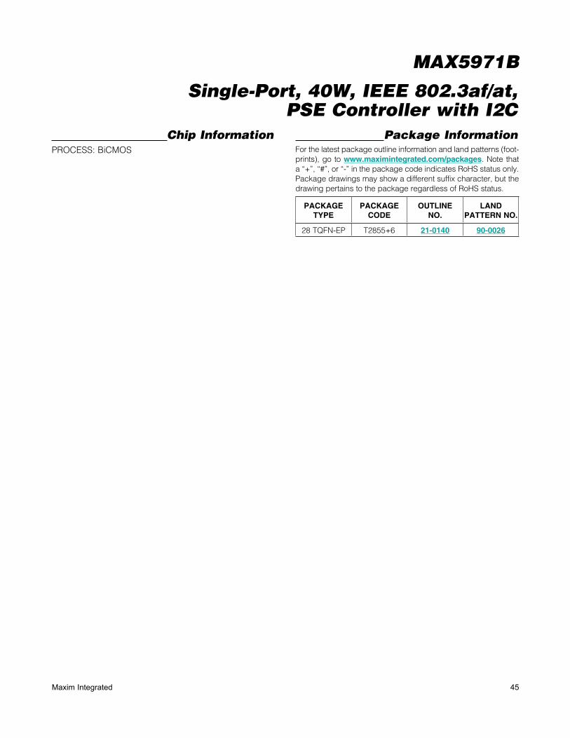
45Maxim Integrated
Single-Port, 40W, IEEE 802.3af/at, PSE Controller with I2C
MAX5971B
Package InformationFor the latest package outline information and land patterns (foot-prints), go to www.maximintegrated.com/packages. Note that a “+”, “#”, or “-” in the package code indicates RoHS status only. Package drawings may show a different suffix character, but the drawing pertains to the package regardless of RoHS status.
Chip InformationPROCESS: BiCMOS
PACKAGE TYPE
PACKAGE CODE
OUTLINENO.
LAND PATTERN NO.
28 TQFN-EP T2855+6 21-0140 90-0026

Single-Port, 40W, IEEE 802.3af/at, PSE Controller with I2C
MAX5971B
Maxim Integrated cannot assume responsibility for use of any circuitry other than circuitry entirely embodied in a Maxim Integrated product. No circuit patent licenses are implied. Maxim Integrated reserves the right to change the circuitry and specifications without notice at any time. The parametric values (min and max limits) shown in the Electrical Characteristics table are guaranteed. Other parametric values quoted in this data sheet are provided for guidance.
46 Maxim Integrated 160 Rio Robles, San Jose, CA 95134 USA 1-408-601-1000© 2016 Maxim Integrated Products, Inc. Maxim Integrated and the Maxim Integrated logo are trademarks of Maxim Integrated Products, Inc.
Revision History
REVISIONNUMBER
REVISIONDATE
DESCRIPTIONPAGES
CHANGED
0 6/10 Initial release —
1 12/10 Updated current-limit, overcurrent, and ADC specifications for rev 3 silicon2, 3, 6, 26–28
2 4/11 Corrected the I2C section, Figure 14, and other minor edits throughout data sheet.
1, 2, 4–11, 13, 14, 18, 19, 21,
25–27, 29–31, 34, 35, 37, 39, 41–43
3 3/16 Changed temperature range from “-40°C to +85°C” to “-40°C to +105°C” globally