Embed Size (px)
Citation preview
January 2014EB83_01.0
iCE40LM4K Sensor Evaluation KitUser’s Guide
2
iCE40LM4K Sensor Evaluation Kit
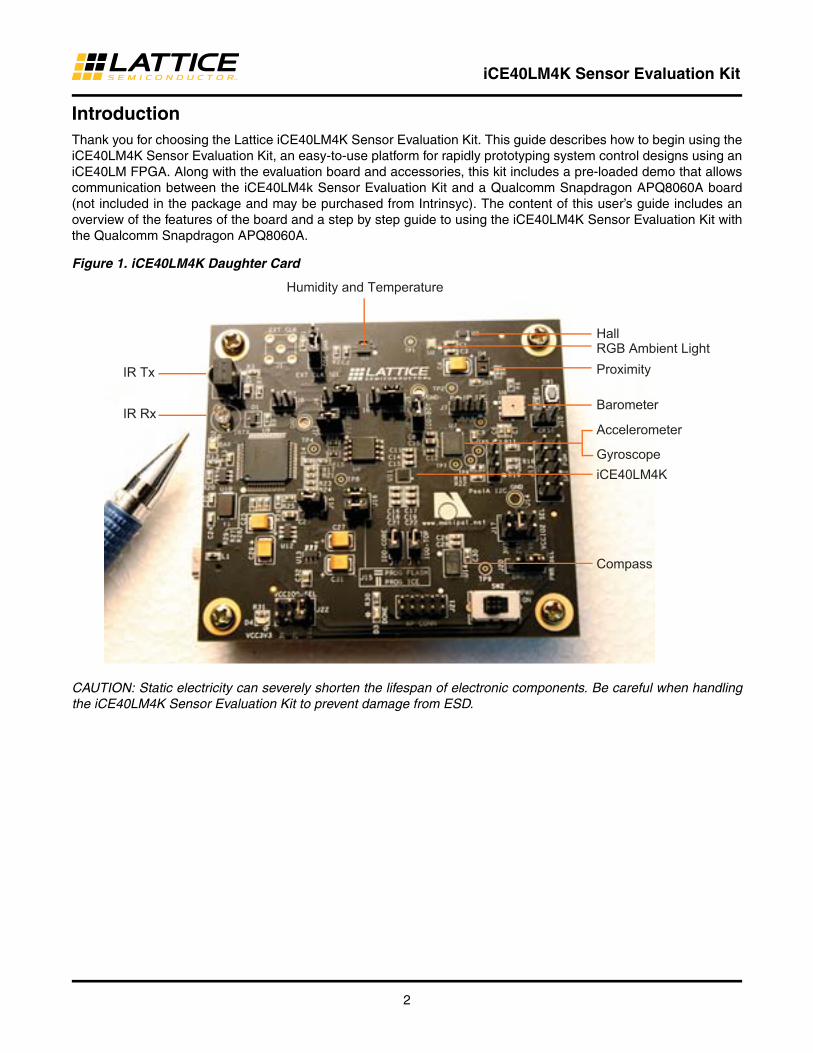
IntroductionThank you for choosing the Lattice iCE40LM4K Sensor Evaluation Kit. This guide describes how to begin using the iCE40LM4K Sensor Evaluation Kit, an easy-to-use platform for rapidly prototyping system control designs using an iCE40LM FPGA. Along with the evaluation board and accessories, this kit includes a pre-loaded demo that allows communication between the iCE40LM4k Sensor Evaluation Kit and a Qualcomm Snapdragon APQ8060A board (not included in the package and may be purchased from Intrinsyc). The content of this user’s guide includes an overview of the features of the board and a step by step guide to using the iCE40LM4K Sensor Evaluation Kit with the Qualcomm Snapdragon APQ8060A.
Figure 1. iCE40LM4K Daughter Card
CAUTION: Static electricity can severely shorten the lifespan of electronic components. Be careful when handling the iCE40LM4K Sensor Evaluation Kit to prevent damage from ESD.
IR Tx
Humidity and Temperature
IR Rx
HallRGB Ambient LightProximity
Barometer
Accelerometer
GyroscopeiCE40LM4K
Compass
3
iCE40LM4K Sensor Evaluation Kit
FeaturesThe iCE40LM4K Sensor Evaluation Kit includes:
• iCE40LM4K Evaluation Board – The ICE40LM4k Evaluation Board features the following on-board compo-nents and circuits:
– iCE40LM4K Device in the 25 WLCSP Package– High-Current LED Output– Infrared Transmit and Receive – Barcode LED/Emulation– Configuration SPI Flash– On-board FT2232HL for USB Programming/Interface– Numerous Sensors– Proximity Sensor (AMS-TAOS TMD27711)– RGB Color, Infrared, and Temperature Sensors (Maxim MAX44006)– Barometric Pressure Sensor (Bosch BMP085)– Accelerometer and Gyro (ST Micro LSM330DLC)– Magnetometer/Compass/Accelerometer (ST Micro LSM303DLHCTR)– Humidity and Temperature Sensor (Sensirion SHT20)– Hall Sensor (Rohm BU52051NVX)
• SMA Connector for External Clock Input
• On-Board Oscillator
In addition to the iCE40LM4K Evaluation Board, an adapter board for connection to Dragon Board and a connector cable are also included. This secondary PCB connected by a cable allows the iCE40LM4k Sensor Evaluation Kit to interface with a Qualcomm 8060A Dragon Board (Dragon Board is available separately and not sold by Lattice). When connected properly, a sensor hub demonstration can be conducted.
4
iCE40LM4K Sensor Evaluation Kit
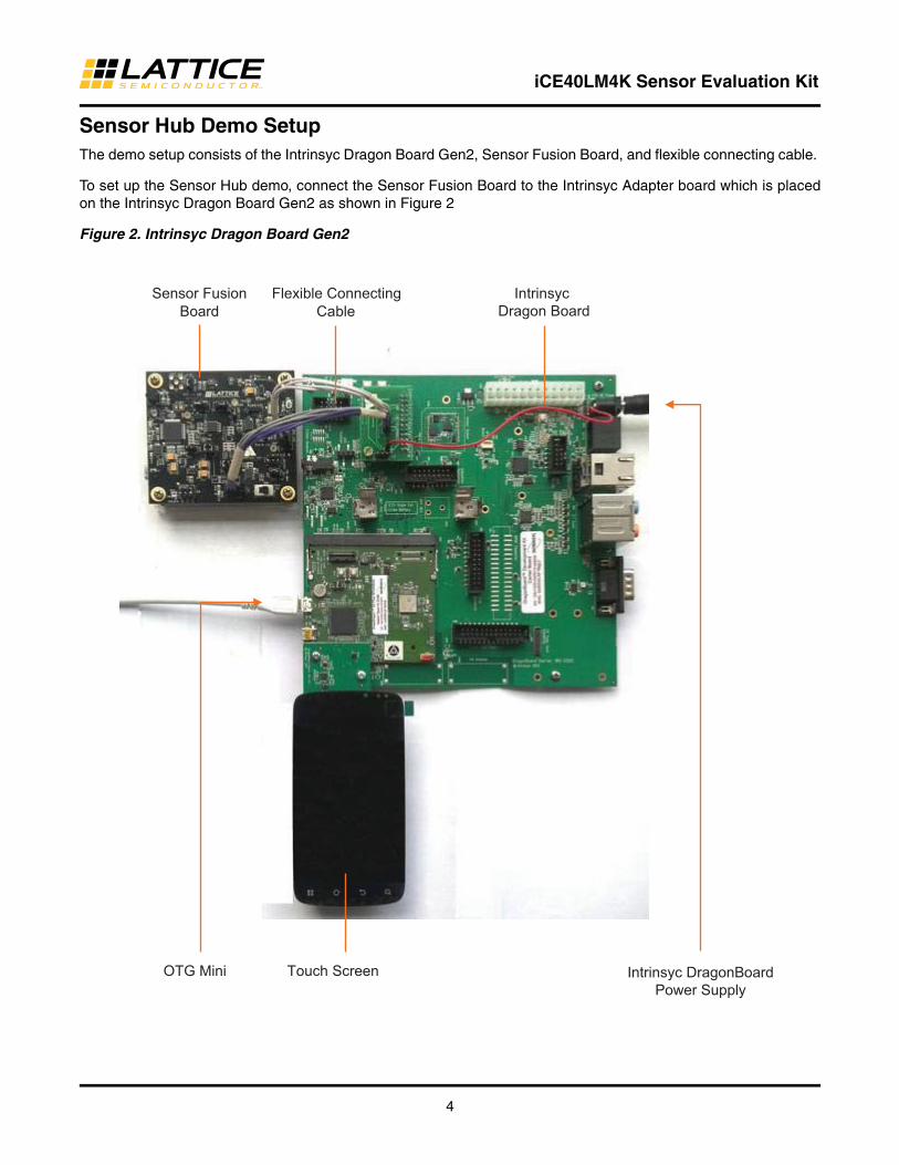
Sensor Hub Demo SetupThe demo setup consists of the Intrinsyc Dragon Board Gen2, Sensor Fusion Board, and flexible connecting cable.
To set up the Sensor Hub demo, connect the Sensor Fusion Board to the Intrinsyc Adapter board which is placed on the Intrinsyc Dragon Board Gen2 as shown in Figure 2
Figure 2. Intrinsyc Dragon Board Gen2
Sensor Fusion Flexible Connecting Intrinsyc Dragon Board
Board Cable
OTG Mini Touch Screen Intrinsyc DragonBoardPower Supply

5
iCE40LM4K Sensor Evaluation Kit
Sensor Fusion Board Default Jumper SettingsThis section provides the details of the Sensor Fusion Board jumper settings:
• Set J2 jumper on OSC mode in EXT CLK.
• Set J4 jumper on BAR.
• Set J5 jumper on HALL.
• Do not set J7 jumper.
• Set J8 jumper.
• Do not set J10 jumper.
• Do no set J11 jumper.
• Set J12 jumper.
• Do not set J15 jumper.
• Set both the J16 jumpers vertically.
• Set jumper on IDD-CORE and IDD-TOP (J18 & J19).
• Set VCCIO0 (J22) to 1.8V.
• Set VCCIO2 (J17) set to 3.3V.
• Set J20 jumper on USB mode.
Connecting the Sensor Fusion Board to the Intrinsyc Dragon BoardTo connect the Sensor Fusion Board to the Intrinsyc Dragon Board
1. Power-off the Intrinsyc Dragon Board.
2. Connect the Intrinsyc Dragon Board end of the processor configuration cable to the Intrinsyc Adapter board mounted on the Intrinsyc Dragon Board.
i. The marked pin of the cable connector should be connected to pin 1 of the connector on the Intrinsyc Adapter board near the white dot.
3. Connect the smaller connector on other end of the cable to the J21 connector of the Sensor Fusion Board.i. The marked pin of the cable connector should be connected to pin 1 of the J21 connector near the
white dot.4. Connect the larger connector on the other end of the cable to the J13 connector of the Sensor Fusion Board.
i. The marked pin of the cable connector should be connected to pin 1 of the J21 connector near the white dot.
5. Power-on the Intrinsyc Dragon Board after the above connections are completed.
Note: Do not connect the mini USB power cable to the Sensor Fusion Board when it is connected to the Intrinsyc Dragon Board.
6
iCE40LM4K Sensor Evaluation Kit
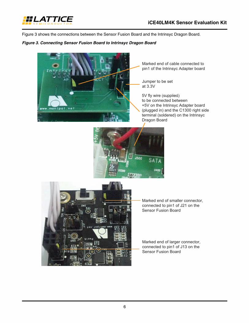
Figure 3 shows the connections between the Sensor Fusion Board and the Intrinsyc Dragon Board.
Figure 3. Connecting Sensor Fusion Board to Intrinsyc Dragon Board
5V fly wire (supplied) to be connected between +5V on the Intrinsyc Adapter board (plugged in) and the C1300 right side terminal (soldered) on the Intrinsyc Dragon Board
Jumper to be setat 3.3V
Marked end of cable connected topin1 of the Intrinsyc Adapter board
Marked end of smaller connector,connected to pin1 of J21 on theSensor Fusion Board
Marked end of larger connector,connected to pin1 of J13 on theSensor Fusion Board
7
iCE40LM4K Sensor Evaluation Kit
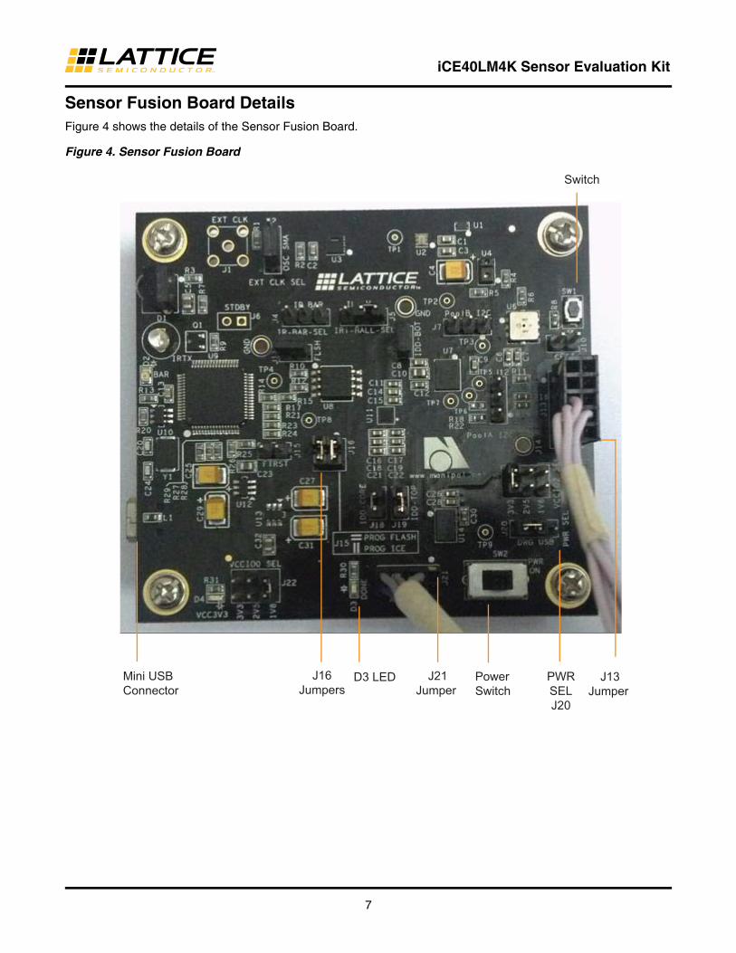
Sensor Fusion Board DetailsFigure 4 shows the details of the Sensor Fusion Board.
Figure 4. Sensor Fusion Board
D3 LED
PowerSwitch
Mini USBConnector
J16Jumpers
J21Jumper
Switch
PWRSELJ20
J13Jumper

8
iCE40LM4K Sensor Evaluation Kit
Flashing System Image and Boot Image to Intrinsyc Dragon BoardNote that this procedure is not required if the Intrinsyc Dragon Board has already been flashed with the system image and boot image (cd Lightning_Demos_Drop_WITH_APK_INSTALL/Dragonboard_boot_images/).
To flash the system image and boot image to the Intrinsyc Dragon Board:
1. Connect the Intrinsyc Dragon Board USB port to your host system through the OTG (mini-USB).i. Download and install android-sdk. Android-sdk for Linux and Windows environment at
http://developer.android.com/sdk/index.html. Set <Installation path>/android_sdk/platform-tools/ to the PATH variable.
2. Run the command below in the terminal/command prompt.#sudo –sNote: This command is applicable only for Linux machines. For Windows machine administrative permission is necessary.
3. Reboot the Intrinsyc Dragon Board in fastboot mode.i. Keep Button Vol / Zoom + pressed on the Intrinsyc Dragon Board during restart.
If the board is already On in adb mode, use the command below for fastboot mode#adb reboot bootloader
ii. When the Intrinsyc Dragon Board is in FASTBOOT mode, a white screen comes on with only Intrinsyc name displayed on it.
iii. Execute the command below in the terminal/command prompt to list the fastboot device number and its name. #fastboot devices
The board is now ready to be flashed with boot.img.
4. Enter the command below to flash system image.#fastboot flash system system.img
If flashing is successful, OKAY and Finished comments are displayed on the terminal.
5. Enter the command below to flash boot.img#fastboot flash boot boot.img
If flashing is successful, OKAY and Finished comments are displayed on the terminal.
6. Enter the command below reboot the board for current boot.img.#fastboot reboot
7. After reboot, go to Settings > Developer options > Stay awake.
9
iCE40LM4K Sensor Evaluation Kit
Installing Sensor Hub apk to AndroidTo flash the system image and boot image to the Intrinsyc Dragon Board:
1. Connect the Intrinsyc Dragon Board USB port to your host system through the OTG (mini-USB).2. Run the command below in the terminal/command prompt.
#sudo –sNote: This command is applicable only for Linux machines. For Windows machine administrative permission is necessary.
3. Use below commands on the terminal to establish and verify 'adb' connection.#adb kill-server#adb start-server#adb devices
If the connection is successful, the device id is displayed on the terminal.4. Run the command below to install the Sensor Hub apk to the Intrinsyc Dragon Board.
#cd Lightning_Demos_Drop_WITH_APK_INSTALL/Sensor_Hub_Demo_Quick_Strart /Android_Apllication
Note: This step should be performed only if not currently in the
Lightning_Demos_Drop_WITH_APK_INSTALL/Sensor_Hub_Demo_Quick_start/Android_Apllication/ folder
#adb install Sensor_Hub_Demo.apk
Demo ProcedureTo execute the demo:
1. Restart Intrinsyc Dragon Board by removing and re-plugging in the power supply, with the Sensor Fusion Board connected to it.When connecting the Sensor Fusion Board to Intrinsyc Dragon Board, make sure that jumper J20 on the Sen-sor Fusion Board is in DRG mode.
2. Wait for Android boot sequence to complete and the home screen to appear.3. Unlock the screen. Go to the Android application menu and open Sensor_Hub_LP3.5k_Intrinsyc.4. Wait for the Processor Configuration to be completed. This is indicated by the lighting of the D3 LED on the
Sensor Fusion board.5. The sensor data is displayed on the Sensor_Hub_LP3.5k_Intrinsyc application.
10
iCE40LM4K Sensor Evaluation Kit
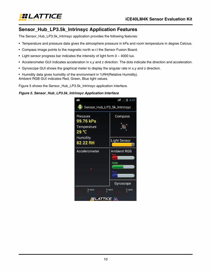
Sensor_Hub_LP3.5k_Intrinsyc Application FeaturesThe Sensor_Hub_LP3.5k_Intrinsyc application provides the following features:
• Temperature and pressure data gives the atmosphere pressure in kPa and room temperature in degree Celcius.
• Compass image points to the magnetic north w.r.t the Sensor Fusion Board.
• Light sensor progress bar indicates the intensity of light form 0 – 4000 lux.
• Accelerometer GUI indicates acceleration in x,y and z direction. The dots indicate the direction and acceleration.
• Gyroscope GUI shows the graphical meter to display the angular rate in x,y and z direction.
• Humidity data gives humidity of the environment in %RH(Relative Humidity).Ambient RGB GUI indicates Red, Green, Blue light values.
Figure 5 shows the Sensor_Hub_LP3.5k_Intrinsyc application interface.
Figure 5. Sensor_Hub_LP3.5k_Intrinsyc Application Interface
11
iCE40LM4K Sensor Evaluation Kit
TroubleshootingIf the Android application does not respond, perform the following procedure:
1. Close the Sensor_Hub_LP3.5k_intrinsyc process running in background.In the Android menu, go toSettings > Applications > Manage Applications > Sensor_Hub_LP3.5k_intrinsyc Force Stop
2. Restart the Intrinsyc Dragon Board.3. Open the Sensor_Hub application from Android menu and application is ready to receive all sensor’s data.4. If the android application crashes while being opened, it means that the library file has not been copied.
Run the command below to install the Sensor Hub apk to the Intrinsyc Dragon Board.#cd Lightning_Demos_Drop_WITH_APK_INSTALL/Sensor_Hub_Demo_Quick_Strart /Android_Apllication
Note: This step should be performed only if not currently in the
Lightning_Demos_Drop_WITH_APK_INSTALL/Sensor_Hub_Demo_Quick_start/Android_Apllication/ folder
#adb install Sensor_Hub_Demo.apk

12
iCE40LM4K Sensor Evaluation Kit
Technical Support Assistancee-mail: [email protected]
Internet: www.latticesemi.com
Revision History
© 2014 Lattice Semiconductor Corp. All Lattice trademarks, registered trademarks, patents, and disclaimers are as listed at www.latticesemi.com/legal. All other brand or product names are trademarks or registered trademarks of their respective holders. The specifications and information herein are subject to change without notice.
Date Version Change Summary
January 2014 01.0 Initial release.
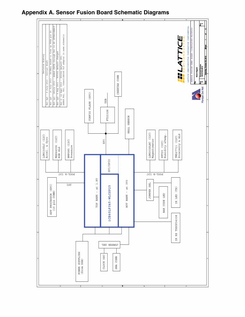
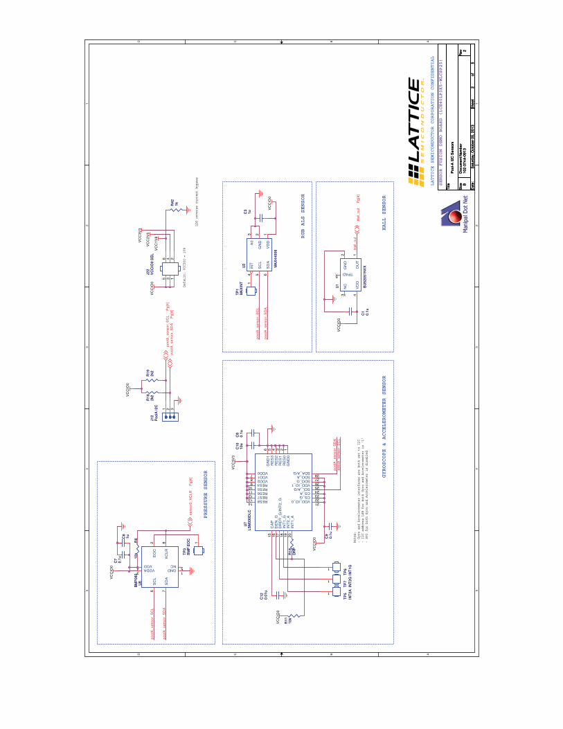
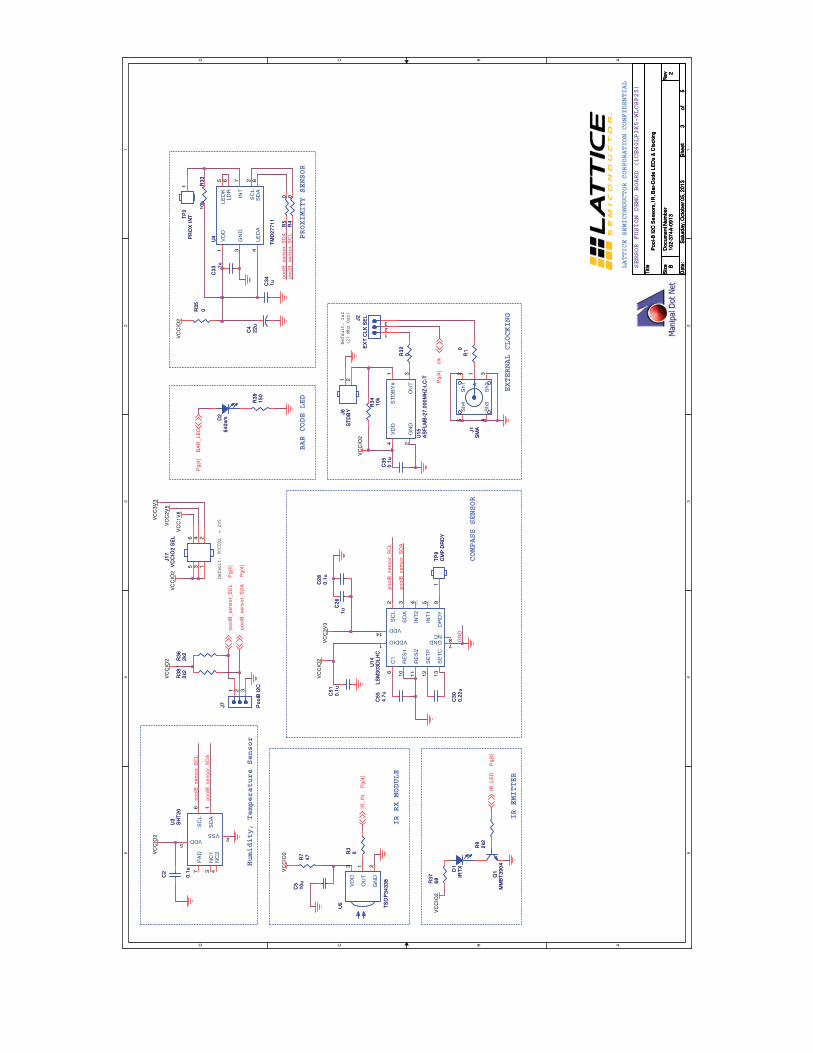
Appendix A. Sensor Fusion Board Schematic Diagrams
5 5
4 4
3 3
2 2
1 1
DD
CC
BB
AA
iCE40LP3k5-WLCSP25
TOP BANK - at 1.8V
MAX44006 (I2C)
RGB ALS
LSM303DLHC (I2C)
Magentometer
APP PROCESSOR (SPI)
(10 pin CONN)
BOT BANK - at 3V3
BMP085 (I2C)
Pressure
SHT20 (I2C)
Humidity &Temp.
IR LED (TX)
IR RX TSSOP34338
BAR CODE LED
JUMPER SEL
POOL-B I2CPOOL-A I2C
SPI
POWER SUPPLIES
(from USB)
CLOCK OSC
SMA CONN
JUMPER SEL
FT2232H
SPI
CONFIG FLASH (SPI)
SPI/GPIO
USB
CHEETAH CONN
LATTICE SEMICONDUCTOR CORPORATION CONFIDENTIAL
SENSOR FUSION DEMO BOARD (iCE40LP3K5-WLCSP25)
Revision History
Rev 0p0 - 9 July 2013 - Initial draft
TMD27711 (I2C)
Proximity & ALS
LSM330DLC (I2C)
Accel. & Gyro
HALL SENSOR
Rev 1p0 - 16 July 2013 - IR/HALL muxed to free up FPGA pin D3
Rev 1p1- 18July 2013 - Added CRSTb through R41 to AP INTERCONNECT
Rev 1p2- 6 Aug 2013 - VCCIO2 default changed
Rev 2- 14 Sept 2013 - VCCIO2 default 3V3,
Added R42, R43, consolidated VLT adapter in same schematic
Titl
e
Siz
eD
ocum
ent N
umbe
rR
ev
Dat
e:
She
eto
f
10
2-3
74
A-0
91
32
Blo
ck D
iagr
am
B
15
Sat
urd
ay, O
ctob
er 0
5, 2
013
Titl
e
Siz
eD
ocum
ent N
umbe
rR
ev
Dat
e:
She
eto
f
10
2-3
74
A-0
91
32
Blo
ck D
iagr
am
B
15
Sat
urd
ay, O
ctob
er 0
5, 2
013
Titl
e
Siz
eD
ocum
ent N
umbe
rR
ev
Dat
e:
She
eto
f
10
2-3
74
A-0
91
32
Blo
ck D
iagr
am
B
15
Sat
urd
ay, O
ctob
er 0
5, 2
013
5 5
4 4
3 3
2 2
1 1
DD
CC
BB
AA
PRESSURE SENSOR
Default: VCCIO0 = 1V8
LATTICE SEMICONDUCTOR CORPORATION CONFIDENTIAL
Notes:
- Gyro and Accelerometer interfaces are both set to I2C
- I2C address LSB for both Gyro and Accelerometer is '1'
- SPI for both Gyro and Accelerometer is disabled
SENSOR FUSION DEMO BOARD (iCE40LP3K5-WLCSP25)
GYROSCOPE & ACCELEROMETER SENSOR
HALL SENSOR
RGB ALS SENSOR
LDO reverse current bypass
pool
A_s
enso
r_S
CL
pool
A_s
enso
r_S
DA
pool
A_s
enso
r_S
DA
pool
A_s
enso
r_S
CL
pool
A_s
enso
r_S
DA
pool
A_s
enso
r_S
CL
Hal
l_ou
t
VC
CIO
0
VC
CIO
0
VC
CIO
0
VC
C1V
8
VC
C2V
5
VC
C3V
3
VC
CIO
0
VC
C3V
3
VC
CIO
0
VC
CIO
0
VC
CIO
0
pool
A_s
enso
r_S
DA
Pg[
4]po
olA
_sen
sor_
SC
LP
g[4]
sens
or0
_X
CL
RP
g[4
]
Hal
l_ou
tP
g[4]
Titl
e
Siz
eD
ocum
ent N
umbe
rR
ev
Dat
e:
She
eto
f
10
2-3
74
A-0
91
32
Po
ol-A
I2C
Se
nso
rs
B
25
Sat
urd
ay, O
ctob
er 0
5, 2
013
Titl
e
Siz
eD
ocum
ent N
umbe
rR
ev
Dat
e:
She
eto
f
10
2-3
74
A-0
91
32
Po
ol-A
I2C
Se
nso
rs
B
25
Sat
urd
ay, O
ctob
er 0
5, 2
013
Titl
e
Siz
eD
ocum
ent N
umbe
rR
ev
Dat
e:
She
eto
f
10
2-3
74
A-0
91
32
Po
ol-A
I2C
Se
nso
rs
B
25
Sat
urd
ay, O
ctob
er 0
5, 2
013
R18
DN
PR
18D
NP
C9
0.1
uC
90
.1u
TP
7IN
T2
GT
P7
INT
2G1
BM
P08
5U
6B
MP
085
U6
SC
L6
SD
A7
XC
LR
8
EO
C2
VDDA3
VDD4 GND
1
NC5
TP
1M
AX
INT
TP
1M
AX
INT 1
C6
1u
C6
1u
TP
5IN
T2
AT
P5
INT
2A1
TP
3B
MP
EO
CT
P3
BM
P E
OC
1R6
10
kR
61
0k
U2
MA
X44
006
U2
MA
X44
006
VD
D1
GN
D2
A0
3IN
T4
SC
L5
SD
A6
TP
6IN
T1
GT
P6
INT
1G1
J22
VC
CIO
0 S
EL
J22
VC
CIO
0 S
EL
246
135
R11
10
kR
111
0k
U1
BU
5205
1NV
X
U1
BU
5205
1NV
XOU
T1
GN
D2
NC
3
VD
D4
TPAD5
C8
0.1
uC
80
.1u
R42
1k
R42
1k
U7
LS
M3
30
DL
CU
7L
SM
33
0D
LC
RE
S0
2
GN
D0
1
RES814
RES713
RES612
RES511
RES410
VDD07
CA
P15
DE
N_G
16
DR
DY
_G
/IN
T2_G
17
INT
1_G
18
INT
2_A
19
INT
1_A
20
VDD_IO_021
CS_G22
CS_A23
SCL_A/G24
VDD_IO_125
SDO_G26
RE
S1
3R
ES
24
RE
S3
5G
ND
16
VDD18 VDD29
SDO_A27
SDA_A/G28
R16
2k2
R16
2k2
J12
Po
olA
I2C
J12
Po
olA
I2C
1 2 3
C10
10
uC
101
0u
C12
0.0
1u
C12
0.0
1u
R19
2k2
R19
2k2
C1
0.1
uC
10
.1u
C7
0.1
uC
70
.1u
C3
1u
C3
1u
5 5
4 4
3 3
2 2
1 1
DD
CC
BB
AA
Humidity, Temperature Sensor
IR RX MODULE
IR EMITTER
EXTERNAL CLOCKING
BAR CODE LED
Default: VCCIO2 = 2v5
Default: 1&2
(27 Mhz Osc)
LATTICE SEMICONDUCTOR CORPORATION CONFIDENTIAL
PROXIMITY SENSOR
COMPASS SENSOR
SENSOR FUSION DEMO BOARD (iCE40LP3K5-WLCSP25)
pool
B_s
enso
r_S
DA
pool
B_s
enso
r_S
CL
pool
B_s
enso
r_S
CL
pool
B_s
enso
r_S
DA
GN
D
pool
B_s
enso
r_S
CL
pool
B_s
enso
r_S
DA
VC
CIO
2V
CC
IO2
VC
CIO
2
VC
CIO
2
VC
CIO
2
VC
C1V
8
VC
C2
V5
VC
C3V
3
VC
CIO
2
VC
C3V
3V
CC
IO2
VC
CIO
2
pool
B_s
enso
r_S
DA
Pg[
4]
pool
B_s
enso
r_S
CL
Pg[
4]
IR_
INP
g[4
]
BA
R_L
ED
Pg[
4]
IR_
LE
DP
g[4
]
clk
Pg[
4]
Titl
e
Siz
eD
ocum
ent N
umbe
rR
ev
Dat
e:
She
eto
f
10
2-3
74
A-0
91
32
Poo
l-B I2
C S
enso
rs, I
R, B
ar-C
ode
LED
s &
Clo
ckin
g
B
35
Sat
urd
ay, O
ctob
er 0
5, 2
013
Titl
e
Siz
eD
ocum
ent N
umbe
rR
ev
Dat
e:
She
eto
f
10
2-3
74
A-0
91
32
Poo
l-B I2
C S
enso
rs, I
R, B
ar-C
ode
LED
s &
Clo
ckin
g
B
35
Sat
urd
ay, O
ctob
er 0
5, 2
013
Titl
e
Siz
eD
ocum
ent N
umbe
rR
ev
Dat
e:
She
eto
f
10
2-3
74
A-0
91
32
Poo
l-B I2
C S
enso
rs, I
R, B
ar-C
ode
LED
s &
Clo
ckin
g
B
35
Sat
urd
ay, O
ctob
er 0
5, 2
013
R10
R10
Q1
MM
BT
3904
Q1
MM
BT
3904
TP
9C
MP
DR
DY
TP
9C
MP
DR
DY
1
R33
10
kR
331
0k
J7 Po
olB
I2C
J7 Po
olB
I2C
1 2 3
AS
FLM
B-2
7.00
0MH
Z-L
C-T
U1
5A
SF
LMB
-27.
000M
HZ
-LC
-TU
15
GN
D2
VD
D4
ST
DB
Y#
1
OU
T3
J2E
XT
CLK
SE
LJ2E
XT
CLK
SE
L
123
R36
2k2
R36
2k2
C26
1uC
261
u
C34
1u
C34
1u
R37
68
R37
68
TM
D2
77
11
U4
TM
D2
77
11
U4
VD
D1
GN
D3
LE
DA
4S
CL
2
LE
DK
5
LD
R6
INT
7
SD
A8
C28
0.1
uC
280
.1u
C35
0.1
uC
350
.1u
R38
2k2
R38
2k2
C5
10
uC
51
0u
R39
15
0R
391
50
U3
SH
T20
U3
SH
T20
SD
A1
VSS2
NC
13
NC
24
VDD5
SC
L6
PA
D7
C2
0.1
u
C2
0.1
u
U5
TS
OP
34
33
8
U5
TS
OP
34
33
8
VD
D3
OU
T1
GN
D2
R5
0R
50
R32
0R32
0
R4
0R
40
C51
0.1
uC
510
.1u
R9
2k2
R9
2k2
R34 10
kR
34 10
k
R3
0R3
0
R7
47
R7
47
C30
0.2
2u
C30
0.2
2u
R35
0R35
0
D2
64
0nmD
26
40
nm
LS
M3
03
DL
HC
U1
4L
SM
30
3D
LH
CU
14
C1
6
RE
S1
10
RE
S2
11
SE
TP
12
SE
TC
13
SC
L2
SD
A3
INT
24
INT
15
DR
DY
9
VDDIO1
VDD14
GND7
NC8
C55
4.7
uC
554
.7u
C33
1u
C33
1u
J17
VC
CIO
2 S
EL
J17
VC
CIO
2 S
EL 246
135
D1
IRT
XD1
IRT
X
J6S
TD
BYJ6
ST
DB
Y1 2
J1S
MAJ1
SM
AA
1
Sh1
2
Sh2
3S
h3
4
Sh4
5
C4
22
uC
42
2u
TP
2P
RO
X I
NTTP
2P
RO
X I
NT
1
5 5
4 4
3 3
2 2
1 1
DD
CC
BB
AA
SPI CONFIGURATION / FLASH
LATTICE SEMICONDUCTOR CORPORATION CONFIDENTIAL
AP (DRAGON BOARD) INTERCONNECT
Note position of pin#1
in reference board
Note position of pin#1
in reference board
Note:
Place close
to DUT
Note:
Place close
to DUT
Note:
Place close
to DUT
DUT
Default: Shunt
For programming Flash - Shunt 1,3 and 2,4 (default)
For programming iCE - Shunt 3,4 and 1,2
Default: Shunt
Default: Shunt
Default: Open
Default: Shunt
Default: Shunt 1,2 (for IR LED)
SENSOR FUSION DEMO BOARD (iCE40LP3K5-WLCSP25)
pro
c_sd
ip
roc_
sdo
pro
c_in
trp
roc_
sclk
pro
c_cs
CR
ST
b
CD
ON
E
CR
ST
bC
DO
NE
pool
A_s
enso
r_S
CL
pool
A_s
enso
r_S
DA
flsh_
csfls
h_m
osi
flsh_
sclk
flsh_
mis
o
flsh_
mos
ifls
h_m
iso
flsh_
sclk
pool
B_s
enso
r_S
CL
pool
B_s
enso
r_S
DA
flsh_
csfls
h_sc
lk
pro
c_sd
o
pro
c_sd
ip
roc_
intr
pro
c_sc
lkp
roc_
cs
BA
R_L
ED
BA
R_
LE
D_
MU
X_
IR_
LE
DIR
_L
ED
BA
R_
LE
D_
MU
X_
IR_
LE
D
CR
ST
b
flsh_
cs
flsh_
mos
i
ice_
SO
ice_
SI
ice_
SO
flsh_
mis
oic
e_S
I
IR_
ING
PIO
_C
5
GP
IO_
C5
sens
or0
_X
CL
R
Hal
l_o
ut
CR
ST
b
DR
GN
5V
VC
C3V
3
VC
CIO
0
VC
CIO
2
VC
CIO
0
VC
C1V
2
VC
C3V
3
pool
B_s
enso
r_S
DA
Pg
[3]
pool
B_s
enso
r_S
CL
Pg[
3]
pool
A_s
enso
r_S
DA
Pg
[2]
pool
A_s
enso
r_S
CL
Pg
[2]
flsh_
csP
g[5
]
IR_
INP
g[3]
IR_
LE
DP
g[3
]
CR
ST
bP
g[5]
clk
Pg
[3]
flsh_
csP
g[5
]
BA
R_L
ED
Pg[
3]
CD
ON
EP
g[5
]
Hal
l_ou
tP
g[2] fls
h_m
iso
Pg[
5]
flsh_
sclk
Pg[
5]fls
h_cs
Pg[
5]fls
h_m
osi
Pg[
5]
sens
or0
_X
CL
RP
g[2
]
Titl
e
Siz
eD
ocum
ent N
umbe
rR
ev
Dat
e:
She
eto
f
10
2-3
74
A-0
91
32
FP
GA
, Con
fig F
lash
, AP
Inte
rcon
nect
s
B
45
Sat
urd
ay, O
ctob
er 0
5, 2
013
Titl
e
Siz
eD
ocum
ent N
umbe
rR
ev
Dat
e:
She
eto
f
10
2-3
74
A-0
91
32
FP
GA
, Con
fig F
lash
, AP
Inte
rcon
nect
s
B
45
Sat
urd
ay, O
ctob
er 0
5, 2
013
Titl
e
Siz
eD
ocum
ent N
umbe
rR
ev
Dat
e:
She
eto
f
10
2-3
74
A-0
91
32
FP
GA
, Con
fig F
lash
, AP
Inte
rcon
nect
s
B
45
Sat
urd
ay, O
ctob
er 0
5, 2
013
J4
BA
R_
IR_
SE
L
J4
BA
R_
IR_
SE
L
123
C15
1uC
151
u
R40
10
kR
401
0k
R2
0R
20
J11
FL
SH
EN
J11
FL
SH
EN
12
SW
1
CR
ST
SW
1
CR
ST
C1
90
.1u
C19
0.1
u
J8 IDD
_B
OT
J8 IDD
_B
OT
12
C17 10
nC
17 10
n
R12
10
kR
121
0k
D3
DO
NE
D3
DO
NE
J21
AP
IN
TE
RC
ON
NE
CT
J21
AP
IN
TE
RC
ON
NE
CT
2 4 6 810
1 3 5 7 9
C16 10
nC
16 10
n
C22
1u
C22
1u
R30
2k2
R30
2k2
R41
0R
410
R10
10
kR
101
0k
C18
0.1
uC
180
.1u
J13
SP
I PG
MJ1
3S
PI P
GM
SS
21
GN
D1
2
SS
33
NC
24
MIS
O5
NC
16
SC
LK
7M
OS
I8
SS
19
GN
D2
10
C21
1u
C21
1u
TOP BANK
BOT BANK
CONFIG S
PI
iCE40LP3k5-WLCSP25
iCE
40LP
3k5-
WLC
SP
25
U1
1TOP BANK
BOT BANK
CONFIG S
PI
iCE40LP3k5-WLCSP25
iCE
40LP
3k5-
WLC
SP
25
U1
1
IOB
2E
5
IOB
3D
5
IOB
4E
4
IOB
5C
5
IOB
11_G
5E
3IO
B12_G
4C
4
IOB
16
D3
CD
ON
EC
3
CR
ST
BB
3
IOB
22_S
OD
2
IOB
23_S
IC
1
IOB
24_S
CLK
D1
IOB
25_S
SE
1
IOT
28
A1
IOT
30
B1
IOT
31
C2
IOT
45_G
1A
3IO
T46_G
0A
4
IOT
55
B5
IOT
56
A5
AV
DD
/ V
CC
B4
VC
CIO
0A
2
GN
D1
D4
VC
CIO
2/S
PIV
CC
E2
GN
D2
B2
M2
5P
80
U8
M2
5P
80
U8
SD
I5
SC
K6
WP
3
CS
1
SD
O2
HO
LD
7
8
VC
C
4
GN
D
J19
IDD
_T
OP
J19
IDD
_T
OP
12
J18
IDD
_C
OR
EJ1
8ID
D_
CO
RE
12
C38
0.1
uC
380
.1u
C14
0.1
uC
140
.1u
J16
MA
/ S
LJ1
6M
A /
SL
3 41 2
R8
10
kR
81
0k
J5
IR M
UX
J5
IR M
UX
123
R22
2k2
R22
2k2
C11
10
nC
111
0n
J10
CR
ST
J10
CR
ST
12
5 5
4 4
3 3
2 2
1 1
DD
CC
BB
AA
LDO REGULATORS
USB PROGRAMMER
Default: 1&2
(USB 5V)
LATTICE SEMICONDUCTOR CORPORATION CONFIDENTIAL
spread across board, easy access
Default: Open
SENSOR FUSION DEMO BOARD (iCE40LP3K5-WLCSP25)
US
B_D
M
GN
D
FT
_C
RS
T
EP_CS
FT
_C
RS
T
GND
EP
_DI
GND
EP
_CLK
EP
_CS
GN
D
FT
_D
I
FT
_D
IF
T_
SK
FT
_S
K
FT
_C
S
EP_DI
FT
_D
O
FT
_C
S
EP_CLK
GN
D
US
B_D
P
GN
D
FT
_D
O
GN
D
GN
D
USB_DP
USB_DM
FT
_C
DO
NE
FT
_C
DO
NE
VC
C3V
3
VC
C3V
3
VC
C3V
3
FT
VC
OR
VC
C3V
3
FT
VC
OR
VC
C3V
3
FT
VC
OR
FT
VC
OR
VC
C3V
3
VC
C3V
3
VC
C3V
3
VC
C3V
3
VC
C5
V
VC
C1V
2V
CC
1V8
VC
C2V
5V
CC
3V
3
VC
C5V
DR
GN
5V
US
B5V
US
B5V
VC
C5V V
CC
5V
CR
ST
bP
g[4
]
flsh_
mis
oP
g[4
]fls
h_sc
lkP
g[4
]fls
h_cs
Pg[
4]
flsh_
mo
siP
g[4
]
CD
ON
EP
g[4]
Titl
e
Siz
eD
ocum
ent N
umbe
rR
ev
Dat
e:
She
eto
f
10
2-3
74
A-0
91
32
US
B P
rogr
amm
ing
& P
ower
Sup
plie
s
B
55
Sat
urd
ay, O
ctob
er 0
5, 2
013
Titl
e
Siz
eD
ocum
ent N
umbe
rR
ev
Dat
e:
She
eto
f
10
2-3
74
A-0
91
32
US
B P
rogr
amm
ing
& P
ower
Sup
plie
s
B
55
Sat
urd
ay, O
ctob
er 0
5, 2
013
Titl
e
Siz
eD
ocum
ent N
umbe
rR
ev
Dat
e:
She
eto
f
10
2-3
74
A-0
91
32
US
B P
rogr
amm
ing
& P
ower
Sup
plie
s
B
55
Sat
urd
ay, O
ctob
er 0
5, 2
013
C24
27
pC
242
7p
C50
0.1
uC
500
.1u
C42
0.1
uC
420
.1u
R25
0R
250
C32 1
0u
C32 1
0u
C46
0.1
uC
460
.1u
C40
0.1
uC
400
.1u
L1
10
0M
Hz,
33
0 o
hms
L1
10
0M
Hz,
33
0 o
hms
C29
47
uC
294
7u
J9 GN
DJ9 G
ND
1
R27
10R
2710
R15
0R
150
C52
0.1
uC
520
.1u
C37
10
uC
371
0u
C25
47
uC
254
7u
L3
10
0M
Hz,
33
0 o
hmsL3
10
0M
Hz,
33
0 o
hms
C48
0.1
uC
480
.1u
R17
0R
170
R24
0R
240
C54
0.1
uC
540
.1u
C36
0.1
uC
360
.1u
Y1
12
MH
z
Y1
12
MH
z
MIC
5320
-SJY
D6
TR
U1
2M
IC53
20-S
JYD
6 T
RU
12
3.3
VO
4
3.3
EN
62.5
EN
1
2.5
VO
5
VIN3
GND2
R13
10
kR
131
0k
R21
0R
210
AP
7312
-121
8W6-
7U
13
AP
7312
-121
8W6-
7U
13
1.8
VO
1
1.8
EN
31.2
EN
4
1.2
VO
6
VIN5
GND2
C31
47
uC
314
7u
R20
2k
R20
2k
R26
1k
R26
1k
TP
4S
PT
P4
SP
1
J3 GN
DJ3 G
ND
1
C43
0.1
uC
430
.1u
J14
GN
DJ1
4G
ND
1
C23 1
0u
C23 1
0u
R23
0R
230
C20
27
pC
202
7p
C49
0.1
uC
490
.1u
C45
4.7
uC
454
.7u
J20
PW
R S
EL
J20
PW
R S
EL
123
L2
60
0 o
hm, 5
00
mA
L2
60
0 o
hm, 5
00
mA
R29
12
kR
291
2k
SW
2P
WR
SW
2P
WR
12
3
45
6
78
U9
FT
22
32
H
U9
FT
22
32
H
Gnd_1
1
OS
CI
2
OS
CO
3
VP
HY
4
Gnd_7
5
RE
F6
DM
7
DP
8
VP
LL
9
AG
nd
10
Gnd
11
VC
OR
E_1
12
TE
ST
13
RE
SE
T#
14
Gnd_2
15
AD
BU
S0
16
ADBUS117
ADBUS218
ADBUS319
VCCIO20
ADBUS421
ADBUS522
ADBUS623
ADBUS724
Gnd_325
ACBUS026
ACBUS127
ACBUS228
ACBUS329
ACBUS430
VCCIO_331
ACBUS532
AC
BU
S6
33
AC
BU
S7
34
Gnd_4
35
SU
SP
EN
D#
36
VC
OR
E37
BD
BU
S0
38
BD
BU
S1
39
BD
BU
S2
40
BD
BU
S3
41
VC
CIO
_2
42
BD
BU
S4
43
BD
BU
S5
44
BD
BU
S6
45
BD
BU
S7
46
Gnd_5
47
BC
BU
S0
48
VREGOUT49 VREGIN50 Gnd_651 BCBUS152 BCBUS253 BCBUS354 BCBUS455 VCCIO_156 BCBUS557 BCBUS658 BCBUS759 PWREN#60 EEDATA61 EECLK62 EECS63 VCORE_364
C13
0.1
uC
130
.1u
R31
68
0R
316
80
5VD-
D+ID
G
US
B P
WR
J23
5VD-
D+ID
G
US
B P
WR
J23
1
2
3
4
S2
5
S1
S3
S4
TP
8C
ST
P8
CS
1
C44
4.7
uC
444
.7u
D4
PW
RD4
PW
RC
410
.1u
C41
0.1
u
J15
FT
RS
TJ1
5F
TR
ST
12R
2810
R28
10
C39
0.1
uC
390
.1u
R14
33
0R
143
30
C47
0.1
uC
470
.1u
C27
47
uC
274
7u
93
LC
56
BT
-I/O
TU
10
93
LC
56
BT
-I/O
TU
10
GN
D2
VC
C6
DO
1
DI
3
CLK
4
CS
5
C53
47
uC
534
7u