Embed Size (px)
Citation preview

December 2014EB87_1.1
iCE40 Ultra™ Breakout BoardUser Guide
2
iCE40 Ultra Breakout Board
IntroductionThank you for choosing the Lattice iCE40 Ultra™ Breakout Board.
This guide describes how to begin using the iCE40 Ultra Breakout Board, an easy-to-use platform for demonstrat-ing the high-current LED drive capabilities of the iCE40 Ultra FPGA. Along with the evaluation board and accesso-ries, this kit includes the pre-loaded LED Driver Demo that demonstrates driving the RGB LEDs with a PWM circuit. In addition, most of the device's I/O balls are accessible via one of the several header locations on the board, facil-itating rapid prototyping of user functions.
The contents of this user’s guide include demo operation, top-level functional descriptions of the various portions of the evaluation board, descriptions of the on-board connectors, shunts, a complete set of schematics and the bill of materials for the iCE40 Ultra Breakout Board.
Note: Static electricity can severely shorten the lifespan of electronic components. Be careful when handling the iCE40 Ultra Breakout Board as to not damage it from ESD.
FeaturesThe iCE40 Ultra Breakout Board includes:
• iCE40 Ultra Breakout Board – The iCE40 Ultra Breakout Board features the following on-board components and circuits:
— iCE40 Ultra (iCE5LP4K-SWG36) device in a 36-ball WLCSP package. — Example of a board using this 0.35-pitch WLCSP package. — High-current LED output— Infrared transmit — iCE40 Ultra Current Measurements— Standard USB cable for device programming — RoHS-compliant packaging and process
• Pre-loaded Demo – The kit includes a pre-loaded demo to control the onboard RGB LED in conjunction with a software run GUI.
• USB Connector Cable – A mini B USB port provides power, a programming interface and communication for the software RGB LED GUI to the iCE40 Ultra SPI port.
3
iCE40 Ultra Breakout Board
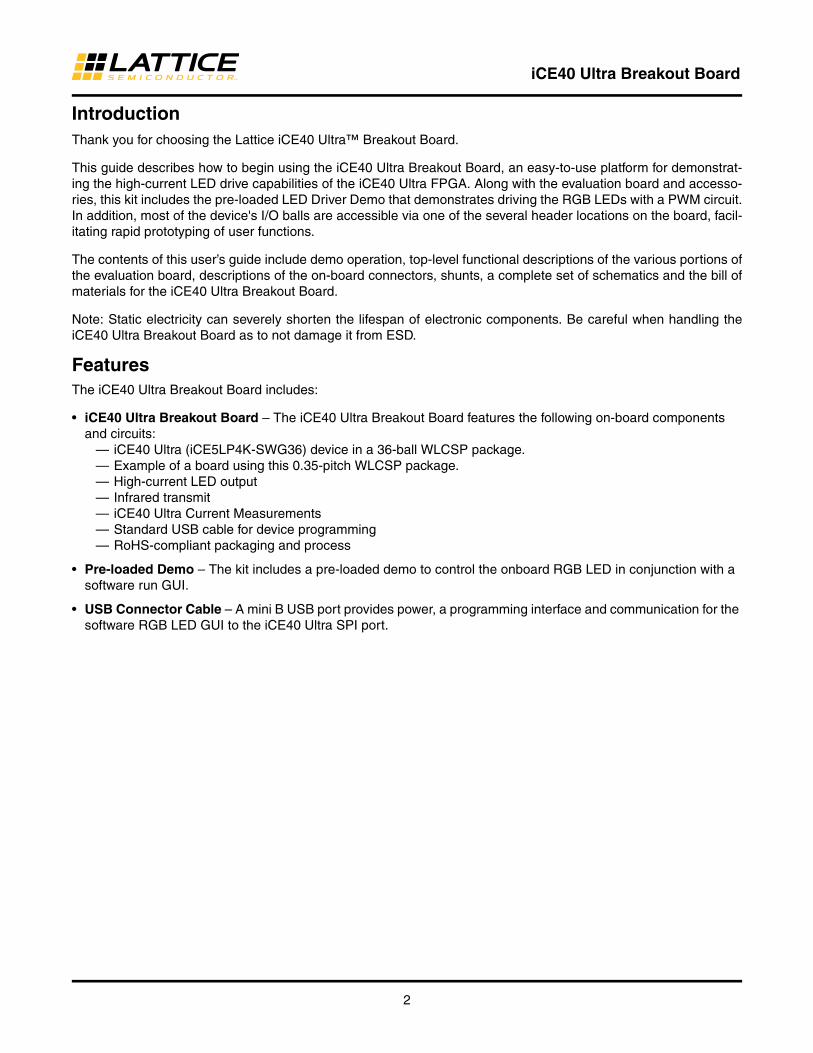
Figure 1 shows the top side of the iCE40 Ultra Breakout Board indicating the specific features that are designed on the board.
Figure 1. iCE40 Ultra Breakout Board (Top Side)
iCE40 Ultra DeviceThe board features an iCE5LP4K FPGA with a 1.2 V core supply. The device is packaged in a 36-ball WLCSP. For a complete description of this device, see DS1048, iCE40 Ultra Family Data Sheet.
Software RequirementsYou should install the following software before you begin developing designs for the board:
• Lattice iCEcube2 2014.04 (or higher)
• Diamond Programmer 3.2 (or higher)
These software are available at the Lattice website Design Software & IP page. Make sure you log in to www.lattic-esemi.com, otherwise these software downloads will not be visible. It is also recommended to download the RGB LED software GUI which interfaces with the iCE40 Ultra Breakout Board. This GUI allows you to control the RGB LED for color, brightness, blinking and breathing. Download the PC or MAC version of the GUI at www.lattice-semi.com.
USB Interface Socket
iCE5LP4K-SWG36
Torch LED
IR LEDRGB LED
D3 – Power LED
4
iCE40 Ultra Breakout Board
Demonstration Design ShuntsLattice provides the RGB LED Driver Demo design programmed in the board. The RGB LED Driver Demo used in conjunction with the software GUI illustrates the use of a PWM driver controlling the LEDs on the board. Below is a description of the control jumpers for each LED.
• The RGB LED will transition colors— J4 can be used to probe RGB LED (Default shunted). If you remove J4, the RGB LED will not light up.
• The IR LED is controlled when a shunt is placed across J50 pins 1-2
• The Bar Code LED is controlled when a shunt is placed across J29 pins 2-3 (Default shunted)
Figure 2 shows the default board shunt locations.
Figure 2. Default Shunt Locations
J3 - Enable DONE LED
J9 – IsolateSPI Flash CSn
J50 – Selects-HP LED device
(IR or Torch)
J51 – Enable-12 MHz clock
J4 – - RGBShunts
J10 – Program SPI Flash or iCE5LP
5
iCE40 Ultra Breakout Board
Clock SourcesThe board has a single 12 MHz clock source. The 12 MHz clock drives both the FTDI USB interface device, and the iCE5LP4K device. The iCE5LP4K can be disconnected from the 12 MHz oscillator using J51. This is necessary, for example, when iCE40 Ultra device ball C2 is mistakenly programmed as an output and prevents the FTDI USB interface from operating.
Board PowerThe board provides the following power features:
• Board Power— Board power is derived from the USB connection.— D3 Green LED indicates Board Power
• iCE40 Ultra VCC— Onboard 1.2 V supply— ICC can be measured across the series resistor R38 (1 Ohm) at TP10 and TP11
• iCE40 Ultra VCCIO— Onboard 3.3 V supply— ICC0 can be measured across the series resistor R14 (1Ohm) at TP1 and TP2— ICC1 can be measured across the series resistor R96 (1Ohm) at TP8 and TP9— ICC2 can be measured across the series resistor R15 (1Ohm) at TP3 and TP4
The power supplies on the iCE40 Ultra Breakout Board are simplified and suitable for booting from the external SPI flash. The power supply sequencing does not conform to the NVCM boot requirements as specified in DS1048, iCE40 Ultra Family Data Sheet. The user may encounter intermittent boot success and/or higher than specified startup currents when attempting to boot from NVCM.
Board Configuration and ProgrammingThe board allows for programming of the iCE40 Ultra or the SPI Flash:
• SPI Flash Programming J10 shunt pins 1-3 and 2-4 (Default shunted)— U7 Micron Technology Inc part number N25Q032A13ESC40F
• iCE40 Ultra Configuration or Programming J10 shunt pins 1-2 and 3-4— U8 iCE5LP4K-SWG36
• CRESETB can be asserted by pushing SW1— Can be probed with J2
• Done LED D2— Can be probed with J3 (Default shunted)
Details of the iCE40 Ultra Board for use in programming are shown in Figure 3.
6
iCE40 Ultra Breakout Board
Figure 3. Configuration and Programming Details
J2 CRESETB Probe
J9 – Isolate SPI Flash CSn
J50 Selects HP LED Device
(IR or Torch)
J10 – Program SPI Flash or iCE5LP
CRESETBPush-Button
D2 – DONE LED
USB Interface Socket
U8 –iCE5LP4K - SWG36
U7 –N25Q032A13ESC40F
–
–

7
iCE40 Ultra Breakout Board
Test PointsThe board features a number of headers and test connections which provide access to the iCE40 Ultra I/Os:
Figure 4. J6 Header ‘A’ Breakouts
Figure 5. J7 Header ‘B’ Breakouts
Figure 6. J5 PMOD Connector
HEADER A
HEADER B
PMOD CONNECTOR
8
iCE40 Ultra Breakout Board
Figure 7. J7 Header ‘B’ Breakouts
The break-out headers and test connectors are shown in Figure 8.
Figure 8. Breakout Headers
AARDVARK CONNECTOR
J6 – “Header A”
J7 – “Header B”
J1 – Aardvark SPI emulator connector
J5 – PMOD Connector
9
iCE40 Ultra Breakout Board
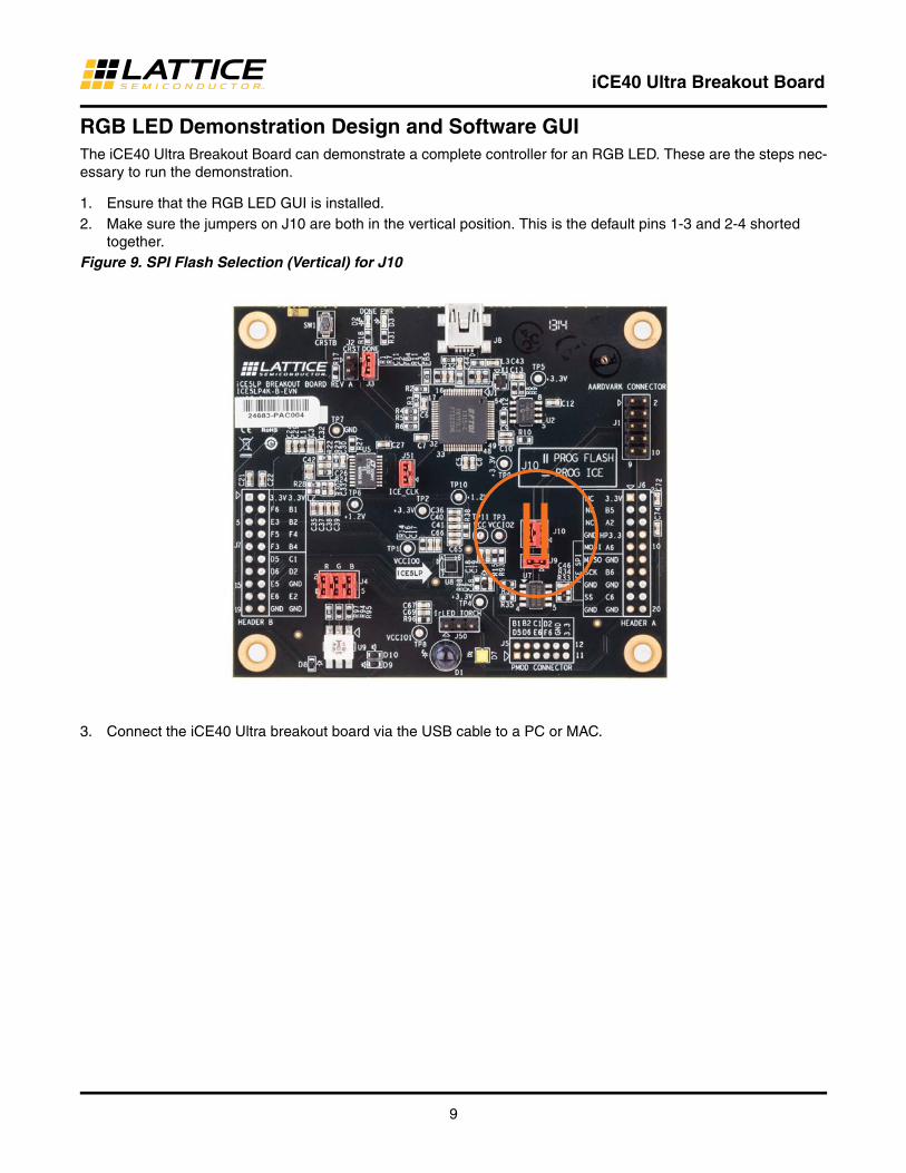
RGB LED Demonstration Design and Software GUIThe iCE40 Ultra Breakout Board can demonstrate a complete controller for an RGB LED. These are the steps nec-essary to run the demonstration.
1. Ensure that the RGB LED GUI is installed.2. Make sure the jumpers on J10 are both in the vertical position. This is the default pins 1-3 and 2-4 shorted
together.Figure 9. SPI Flash Selection (Vertical) for J10
3. Connect the iCE40 Ultra breakout board via the USB cable to a PC or MAC.
10
iCE40 Ultra Breakout Board
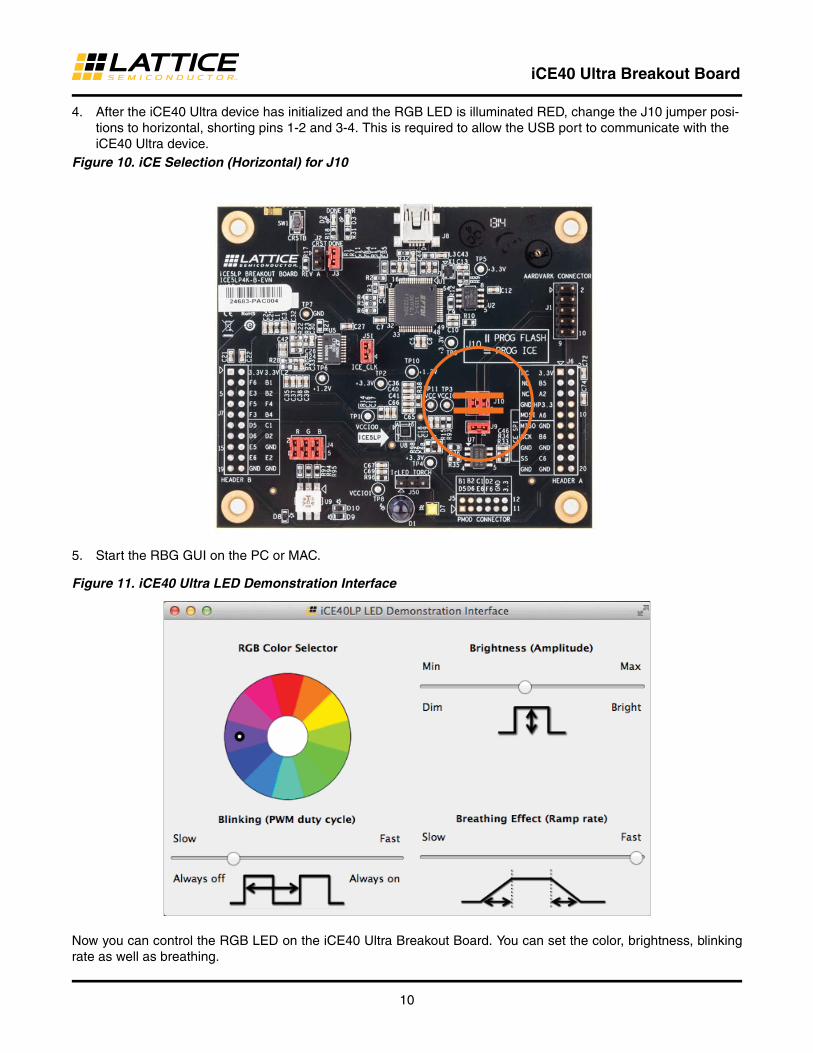
4. After the iCE40 Ultra device has initialized and the RGB LED is illuminated RED, change the J10 jumper posi-tions to horizontal, shorting pins 1-2 and 3-4. This is required to allow the USB port to communicate with the iCE40 Ultra device.
Figure 10. iCE Selection (Horizontal) for J10
5. Start the RBG GUI on the PC or MAC.
Figure 11. iCE40 Ultra LED Demonstration Interface
Now you can control the RGB LED on the iCE40 Ultra Breakout Board. You can set the color, brightness, blinking rate as well as breathing.
11
iCE40 Ultra Breakout Board
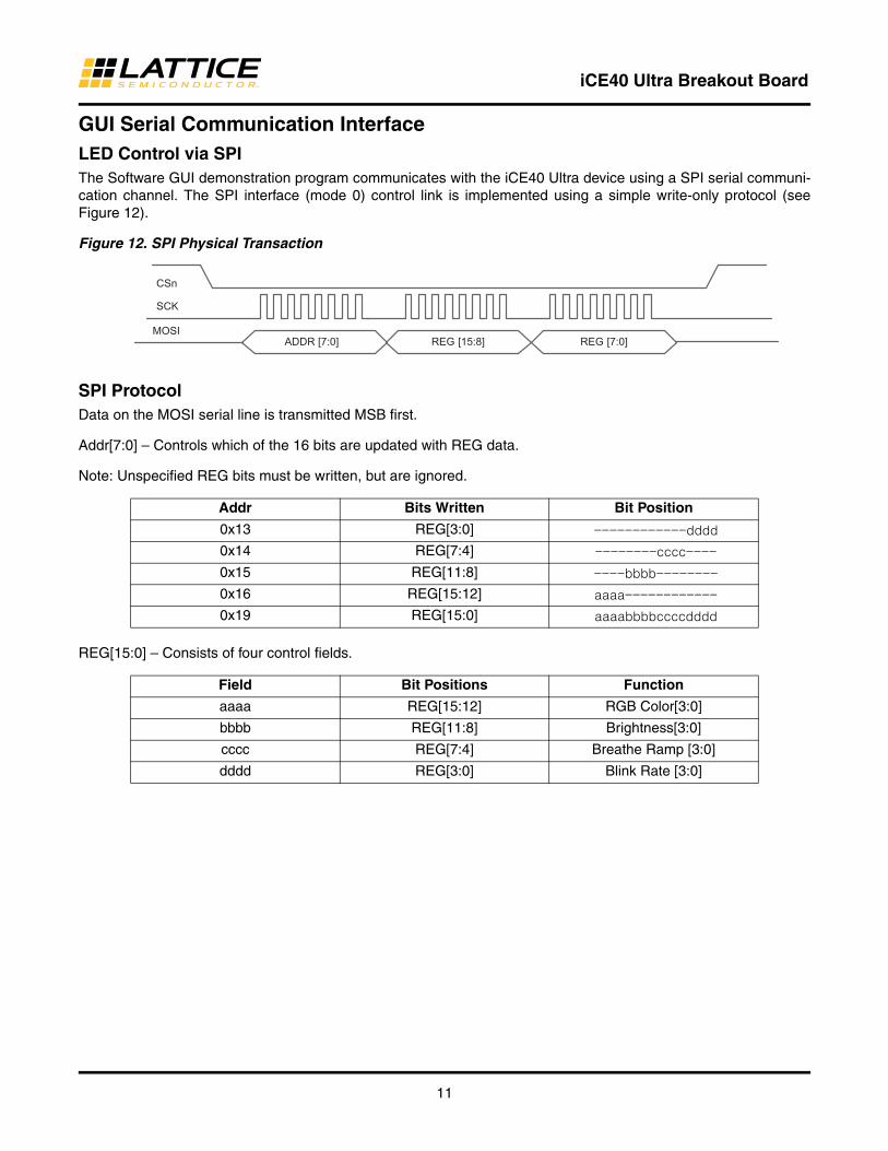
GUI Serial Communication InterfaceLED Control via SPIThe Software GUI demonstration program communicates with the iCE40 Ultra device using a SPI serial communi-cation channel. The SPI interface (mode 0) control link is implemented using a simple write-only protocol (see Figure 12).
Figure 12. SPI Physical Transaction
SPI ProtocolData on the MOSI serial line is transmitted MSB first.
Addr[7:0] – Controls which of the 16 bits are updated with REG data.
Note: Unspecified REG bits must be written, but are ignored.
REG[15:0] – Consists of four control fields.
Addr Bits Written Bit Position
0x13 REG[3:0] ------------dddd
0x14 REG[7:4] --------cccc----
0x15 REG[11:8] ----bbbb--------
0x16 REG[15:12] aaaa------------
0x19 REG[15:0] aaaabbbbccccdddd
Field Bit Positions Function
aaaa REG[15:12] RGB Color[3:0]
bbbb REG[11:8] Brightness[3:0]
cccc REG[7:4] Breathe Ramp [3:0]
dddd REG[3:0] Blink Rate [3:0]
ADDR REG [15:8] REG [7:0]
CSn
SCK
MOSI
[7:0]

12
iCE40 Ultra Breakout Board
Register DefinitionsDefault setting (hardware, software) is denoted by (*).
RGB Color[3:0] Color Color Code
0000* Red #FF0000
0001 Orange #FF7F00
0010 Yellow #FFFF00
0011 Chartreuse #7FFF00
0100 Green #00FF00
0101 Spring Green #00FF7F
0110 Cyan #00FFFF
0111 Azure #007FFF
1000 Blue #0000FF
1001 Violet #7F00FF
1010 Magenta #FF00FF
1011 Rose #FF007F
1100 —
1101 —
1110 —
1111 White #FFFFFF
Brightness[3:0] Level (%)
0000 6.25(dim)
0001 12.5
0010 18.75
0011 25
0100 31.25
0101 37.5
0110 43.75
0111* 50
1000 56.25
1001 62.5
1010 68.75
1011 75
1100 81.25
1101 87.5
1110 93.75
1111 100 (bright)
Breathe Ramp [3:0] Factor
0000* .0x (fast)
0001 .063x
0010 .125x
0011 .25x
0100 .5x
0101 1x
0110 2x
0111 4x (slow)
1000 —
1001 —
1010 —
1011 —
1100 —
1101 —
1110 —
1111 —
Blink Rate [3:0] Off Time (s)1
0000 Always On
0001 1/16 (fast)
0010 1/8
0011 1/4
0100 1/2
0101* 1
0110 2
0111 4
1000 Always Off
1001 —
1010 —
1011 —
1100 —
1101 —
1110 —
1111 —1. By default the LED "On-Time" is fixed at approximately one second.
If desired, the design may be modified so that "On-Time" is symmetrical to the "Off-Time". To do so, replace the file "LED_control.v" with "LED_control_sym.v" and rebuild the design using the iCEcube2 software.
Ordering Information
Description Ordering Part NumberChina RoHS Environment-Friendly Use Period (EFUP)
iCE40 Ultra Breakout Board ICE5LP4K-B-EVN
Technical Support Assistancee-mail: [email protected]
Internet: www.latticesemi.com
Revision History
© 2014 Lattice Semiconductor Corp. All Lattice trademarks, registered trademarks, patents, and disclaimers are as listed at www.latticesemi.com/legal. All other brand or product names are trademarks or registered trademarks of their respective holders. The specifications and information herein are subject to change without notice.
Date Version Change Summary
December 2014 1.1 Updated Board Power section. Added power-supply sequence clarifica-tion note.
June 2014 01.0 Initial release.
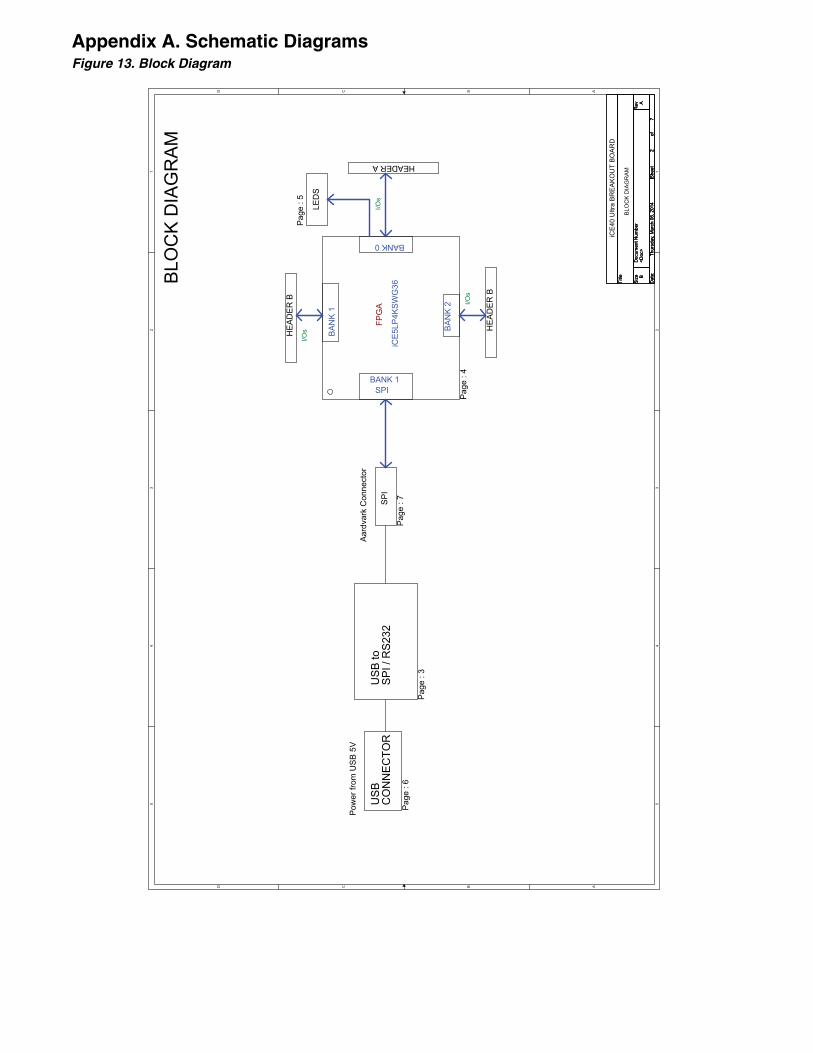
Appendix A. Schematic DiagramsFigure 13. Block Diagram
5 5
4 4
3 3
2 2
1 1
DD
CC
BB
AA
FPG
A
Pow
er fr
om U
SB 5
V
SPI
BANK 0
BAN
K 1
BAN
K 2
iCE5
LP4K
SWG
36
HEA
DER
B
HEA
DER
B
HEADER A
I/Os
I/Os
I/Os
USB
CO
NN
ECTO
RU
SB to
SP
I / R
S232
LED
S
BLO
CK
DIA
GR
AM
iCE
40 U
ltra
BR
EA
KO
UT
BO
AR
D
BLO
CK
DIA
GR
AM
SPI
Page
: 3
Page
: 6
Aard
vark
Con
nect
or
Page
: 7
BANK 1
Page
: 4
Page
: 5
Title
Size
Doc
umen
t Num
ber
Rev
Dat
e:Sh
eet
of
<Doc
>A
B
27
Thur
sday
, Mar
ch 0
6, 2
014
Title
Size
Doc
umen
t Num
ber
Rev
Dat
e:Sh
eet
of
<Doc
>A
B
27
Thur
sday
, Mar
ch 0
6, 2
014
Title
Size
Doc
umen
t Num
ber
Rev
Dat
e:Sh
eet
of
<Doc
>A
B
27
Thur
sday
, Mar
ch 0
6, 2
014
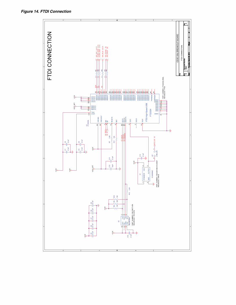
Figure 14. FTDI Connection
5 5
4 4
3 3
2 2
1 1
DD
CC
BB
AA
FTD
I CO
NN
EC
TIO
N
iCE
40 U
ltra
BR
EA
KO
UT
BO
AR
D
FTD
I CO
NN
EC
TIO
N
SCK
SI SO
FT_E
ECS
FT_E
ECLK
FT_E
EDAT
A
SS
+3.3
V
VCC
1_8F
T
VCC
1_8F
T
+3.3
V
+3.3
V
+3.3
V
+3.3
V
+3.3
V
+3.3
V
+3.3
V
ICE_
SCK
[4,5
,7]
FLAS
H_M
OSI
[4,7
]FL
ASH
_MIS
O[4
,7]
ICE_
SS_B
[4,5
,7]
]6[M
D]6[
PD
iCE_
CLK
[4]
ICE_
CD
ON
E[4
]IC
E_C
RES
T[4
]
Title
Size
Doc
umen
t Num
ber
Rev
Dat
e:Sh
eet
of
<Doc
>A
B
37
Thur
sday
, Mar
ch 0
6, 2
014
Title
Size
Doc
umen
t Num
ber
Rev
Dat
e:Sh
eet
of
<Doc
>A
B
37
Thur
sday
, Mar
ch 0
6, 2
014
Title
Size
Doc
umen
t Num
ber
Rev
Dat
e:Sh
eet
of
<Doc
>A
B
37
Thur
sday
, Mar
ch 0
6, 2
014
R3
0
C2
0.1u
F
C6
0.1u
F
R5
0
R7
2.2K
C4
0.1u
F
R4
0
C1
4.7u
F
C7
0.1u
F
R6
0
C3
4.7u
F
J51
2 PI
N J
PR
12
C11
0.1u
F
C8
0.1u
F
FTD
I Hig
h-Sp
eed
USB
F
T223
2H
FT22
32H
LU
1
PAR
T_N
UM
BER
= F
T223
2HL-
REE
LM
anuf
actu
rer =
FTD
I
VRE
GIN
50
VRE
GO
UT
49
DM
7
DP
8
RE
F6
RE
SE
T#14
EE
CS
63
EE
CLK
62
EE
DAT
A61
OS
CI
2
OS
CO
3
TES
T13
ADB
US
016
ADB
US
117
ADB
US
218
ADB
US
319
VPHY4
VPLL9
VCORE12
VCORE37
VCORE64
VCCIO20
VCCIO31
VCCIO42
VCCIO56
AGND10
GND1
GND5
GND11
GND15
GND25
GND35
GND47
GND51P
WR
EN
#60
SU
SP
EN
D#
36
ADB
US
421
ADB
US
522
ADB
US
623
ADB
US
724
ACB
US
026
ACB
US
127
ACB
US
228
ACB
US
329
ACB
US
430
ACB
US
532
ACB
US
633
ACB
US
734
BD
BU
S0
38
BD
BU
S1
39
BD
BU
S2
40
BD
BU
S3
41
BD
BU
S4
43
BD
BU
S5
44
BD
BU
S6
45
BD
BU
S7
46
BC
BU
S0
48
BC
BU
S1
52
BC
BU
S2
53
BC
BU
S3
54
BC
BU
S4
55
BC
BU
S5
57
BC
BU
S6
58
BC
BU
S7
59
C12
0.1u
F
C13
0.1u
F
C9
0.1u
F
93LC
56-S
O8
U2
Man
ufac
ture
r = M
icro
chip
PAR
T_N
UM
BER
= 9
3LC
56C
T-I/S
N
CS
1
CLK
2
DI
3
DO
4VS
S5
OR
G6
NU
7VC
C8
X1
12.0
000M
HZ
PAR
T_N
UM
BER
= D
SC30
01H
E2-0
12.0
000T
Man
ufac
ture
r = M
ircel
VDD
4S
TAN
DB
Y#1
GN
D2
OU
TPU
T3
R12
2.2K
R11
12K
R1
0
R8
10K
R9
10K
C10
10uF
R2
0
C5
0.1u
F
R10
10K
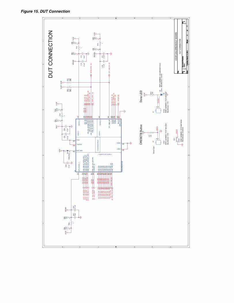
Figure 15. DUT Connection
5 5
4 4
3 3
2 2
1 1
DD
CC
BB
AA
Don
e LE
DC
RES
ETB
Butto
n
Defa
ult:
Ope
n
DU
T C
ON
NE
CTI
ON
iCE
40 U
ltra
BR
EA
KO
UT
BO
AR
D
DU
T C
ON
NE
CTI
ON
CD
ON
EC
RST
b
CD
ON
E
CR
STbCR
STb
ICE
_MIS
O
ICE_
SS_B
ICE
_SC
K
ICE
_MO
SI
IOB_
30A
IOB_
29B
IOB_
27B
IOB_
26A
IOB_
20A
IOB_
16A
IOB_
10A
IOB_
31B
IOB_
7BIO
B_6A
IOB_
11B_
G5
+3.3
VVC
CIO
0
+3.3
V
+1.2
V
+3.3
V
+3.3
V
VCC
IO2
VCC
IO1
+3.3
V+3
.3V
+3.3
V+3
.3V
VCC
ICE_
MO
SI[5
,7]
ICE_
MIS
O[5
,7]
ICE_
SCK
[3,5
,7]
ICE_
SS_B
[3,5
,7]
IOB_
31B
[5]
IOB_
30A
[5]
IOB_
29B
[5]
IOB_
27B
[5]
IOB_
26A
[5]
IOB_
20A
[5]
IOB_
16A
[5]
IOB_
10A
[5]
IOB_
7B[5
]IO
B_6A
[5]
MC
SN0_
SPI2
[5]
SCK_
SPI2
[5]
MO
SI_S
PI2
[5]
MIS
O_S
PI2
[5]
LED
_GR
EEN
[5]
IOT_
46B_
G0
[5]
IOB_
11B_
G5
[5]
HPL
ED[5
]
LED
_RED
[5]
LED
_BLU
E[5
]iC
E_C
LK[3
]ICE_
CD
ON
E[3
]IC
E_C
RES
T[3
]
Title
Size
Doc
umen
t Num
ber
Rev
Dat
e:Sh
eet
of
<Doc
>A
B
47
Tues
day,
Mar
ch 1
1, 2
014
Title
Size
Doc
umen
t Num
ber
Rev
Dat
e:Sh
eet
of
<Doc
>A
B
47
Tues
day,
Mar
ch 1
1, 2
014
Title
Size
Doc
umen
t Num
ber
Rev
Dat
e:Sh
eet
of
<Doc
>A
B
47
Tues
day,
Mar
ch 1
1, 2
014
TP8
DN
I 1
TP11
DN
I 1
C66
0.1u
FD
6C
DBU
0520
1 2
C69
10uF
C17
0.1u
F
R18 2k2
C18
0.1u
F
R96 1
C16
0.1u
F
TP2
DN
I
1
SW1
CR
ST
Man
ufac
ture
r = E
-Sw
itch
PAR
T_N
UM
BER
= T
L101
5AF1
60Q
G
C65
0.1u
F
R14 1
TP3
DN
I
1
TP9
DN
I 1
ICE
5LP
4KS
WG
36
BAN
K 2
BAN
K 0
CONFIG SPI & BANK 1
U8
ICE5
LP4K
SWG
36
VCC
IO_2
C4
IOB
_7B
E5
IOB
_6A
F5
IOB
_5B
_MC
SN
0_S
PI2
D5
IOB
_4A_
SC
K_S
PI2
D6
IOB
_3B
_G6_
MO
SI_
SP
I2E
6
IOB
_2A_
MIS
O_S
PI2
F6
VCC
IO_0
A4
IOT_
46B
_G0
B5
RG
B2
A6
RG
B1
B6
RG
B0
C6
IRLE
DA2
GN
D_L
ED
A1
VPP_2V5D4
VCCPLLB3
VCCA5
GND1A3
GND2C5
SP
I_VC
CIO
_1C
3
IOB
_33B
_SI_
MO
SI_
SP
I1D
1
IOB
_32A
_SO
_MIS
O_S
PI1
F2
IOB
_34A
_SC
K_S
CK
_SP
I1E
1
IOB
_35B
_SS
_MC
SN
O_S
PI1
F1
IOB
_12A
_G4_
CD
ON
EE
4
CR
ES
ET_
BD
3
IOB
_31B
B2
IOB
_30A
C1
IOB
_29B
E2
IOB
_27B
D2
IOB
_26A
B1
IOB
_20A
E3
IOB
_16A
F3
IOB
_10A
B4
IOB
_25B
_G3
C2
IOB
_11B
_G5
F4
TP10
DN
I 1
R93
2.2K
DN
L
D2
Gre
enPA
RT_
NU
MBE
R =
LG
L29
K-G
2J1-
24-Z
Man
ufac
ture
r = O
sram
J2
CR
STPA
RT_
NU
MBE
R =
773
11-8
01-0
2LF
Man
ufac
ture
r = F
CI
12
C67
0.1u
F
C19
10uF
R98
2.2K
DN
L
R38
1
R15 1
TP1
DN
I
1
J3 DO
NE
PAR
T_N
UM
BER
= 7
7311
-801
-02L
FM
anuf
actu
rer =
FC
I
1 2
R17
10k
TP4
DN
I
1
C68
0.1u
F
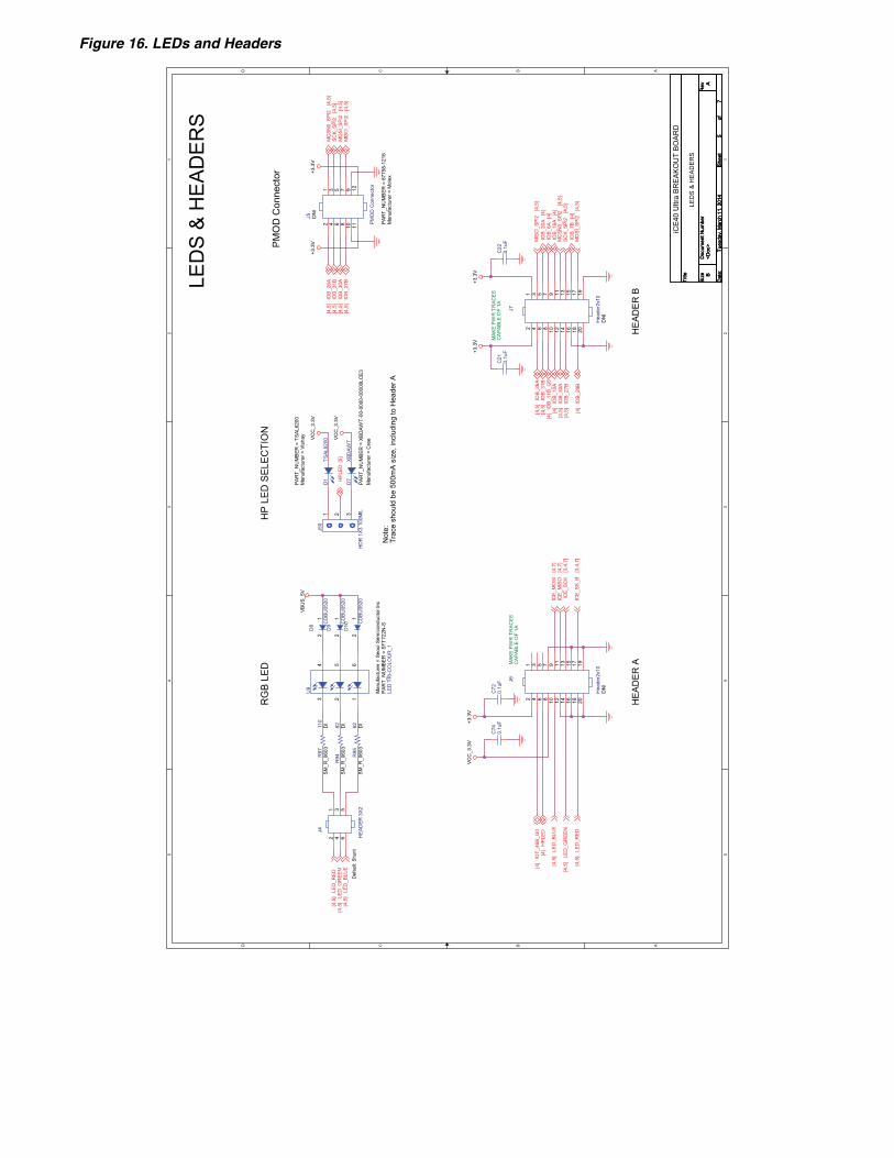
Figure 16. LEDs and Headers
5 5
4 4
3 3
2 2
1 1
DD
CC
BB
AA
Defa
ult:
Shun
t
RG
B LE
D
MAK
E PW
R T
RAC
ESC
APAB
LE O
F 1A
MAK
E PW
R T
RAC
ESC
APAB
LE O
F 1A
PMO
D C
onne
ctor
LED
S &
HE
AD
ER
S
iCE
40 U
ltra
BR
EA
KO
UT
BO
AR
D
LED
S &
HE
AD
ER
S
HE
AD
ER
BH
EA
DE
R A
HP
LED
SEL
ECTI
ON
Not
e:Tr
ace
shou
ld b
e 50
0mA
siz
e, in
clud
ing
to H
eade
r A
+3.3
V+3
.3V
+3.3
V+3
.3V
+3.3
VVC
C_3
.3V
VCC
_3.3
V
VCC
_3.3
V
VBU
S_5V
IOB_
26A
[4,5
]IO
B_31
B[4
,5]
IOB_
30A
[4,5
]IO
B_27
B[4
,5]
MC
SN0_
SPI2
[4,5
]SC
K_SP
I2[4
,5]
MO
SI_S
PI2
[4,5
]M
ISO
_SPI
2[4
,5]
]4[DELP
H
LED
_BLU
E[4
,5] LE
D_G
REE
N[4
,5]
LED
_RED
[4,5
]
ICE_
MO
SI[4
,7]
ICE_
SCK
[3,4
,7]
ICE_
SS_B
[3,4
,7]
ICE_
MIS
O[4
,7]
IOT_
46B_
G0
[4]
IOB_
16A
[4]
IOB_
11B_
G5
[4]
IOB_
26A
[4,5
]IO
B_31
B[4
,5] IO
B_10
A[4
]IO
B_30
A[4
,5]
IOB_
27B
[4,5
]
IOB_
20A
[4]
IOB_
6A[4
]
MIS
O_S
PI2
[4,5
]
MC
SN0_
SPI2
[4,5
]SC
K_SP
I2[4
,5]
MO
SI_S
PI2
[4,5
]IO
B_7B
[4]
IOB_
29B
[4]
HPL
ED[5
]LE
D_G
REE
N[4
,5]
LED
_RED
[4,5
]
LED
_BLU
E[4
,5]
Title
Size
Doc
umen
t Num
ber
Rev
Dat
e:Sh
eet
of
<Doc
>A
B
57
Tues
day,
Mar
ch 1
1, 2
014
Title
Size
Doc
umen
t Num
ber
Rev
Dat
e:Sh
eet
of
<Doc
>A
B
57
Tues
day,
Mar
ch 1
1, 2
014
Title
Size
Doc
umen
t Num
ber
Rev
Dat
e:Sh
eet
of
<Doc
>A
B
57
Tues
day,
Mar
ch 1
1, 2
014
D1
TSAL
6200
PAR
T_N
UM
BER
= T
SAL6
200
Man
ufac
ture
r = V
isha
y
D8 C
DBU
0520
12
D9 C
DBU
0520
12
D10 C
DBU
0520
12
J7
Hea
der2
x10
DN
I
2 4 6 8 10 12 14 16 18 20191715131197531
C22
0.1u
F
R97
110
DI
SM_R
_060
3
R94
62 DI
SM_R
_060
3D
7XB
DAW
T
PAR
T_N
UM
BER
= X
BDAW
T-00
-000
0-00
000L
CE3
Man
ufac
ture
r = C
ree
C72
0.1u
FC
740.
1uF
J6
Hea
der2
x10
DN
I
2 4 6 8 10 12 14 16 18 20191715131197531
U9
LED
TR
I-CO
LOU
R_1
PAR
T_N
UM
BER
= S
FT72
2N-S
Man
ufac
ture
r = S
eoul
Sem
icon
duct
or In
c
4 5 6123
R95
62 DI
SM_R
_060
3
J50
HD
R 1
X3 1
00M
IL1 2 3
J5
PMO
D C
onne
ctor
PAR
T_N
UM
BER
= 8
7758
-121
6M
anuf
actu
rer =
Mol
ex
DN
I
2 4 6 8 10
1 3 5 7 911
12
C21
0.1u
F
J4
HEA
DER
3X2
2 4 6
1 3 5

Figure 17. Regulator Connection
5 5
4 4
3 3
2 2
1 1
DD
CC
BB
AA
RE
GU
LATO
R C
ON
NE
CTI
ON
iCE
40 U
ltra
BR
EA
KO
UT
BO
AR
D
RE
GU
LATO
R C
ON
NE
CTI
ON
+3.3
V
+1.2
V
+3.3
V+1
.2V
VBU
S_5V
VCC
_3.3
V+3
.31V
+1.2
2VVC
C_1
.2V
VBU
S_5V
+3.3
V
+1.2
V
DM
[3]
DP
[3]
Title
Size
Doc
umen
t Num
ber
Rev
Dat
e:Sh
eet
of
<Doc
>A
B
67
Thur
sday
, Mar
ch 0
6, 2
014
Title
Size
Doc
umen
t Num
ber
Rev
Dat
e:Sh
eet
of
<Doc
>A
B
67
Thur
sday
, Mar
ch 0
6, 2
014
Title
Size
Doc
umen
t Num
ber
Rev
Dat
e:Sh
eet
of
<Doc
>A
B
67
Thur
sday
, Mar
ch 0
6, 2
014
C30
0.01
uF
C29
1uF
C31
22uF
C28
10uF
R22
0.1
C37
0.1u
F
R27
210K
L3 600
OH
M 8
00M
A
C42
22uF
C35
10uF
C38
0.1u
FC
33
4.7u
F
C27
10uF
C25
0.01
uF
C39
0.1u
F
TP6
DN
I 1
L2
600
OH
M 8
00M
AC
40
0.1u
F
C41
0.01
uF
C43
0.1u
F
R26
1M
R31
1K
C44
0.1u
F
R25
1M
TP7
DN
I 1
C32
0.1u
F
TP5
DN
I 1
C24
0.1u
F
J8
SKT_
MIN
IUSB
_B_R
A
PAR
T_N
UM
BER
= 5
075B
MR
-05-
SM-C
RM
anuf
actu
rer =
Nel
tron
VCC
1
D-
2
D+
3
ID4
GN
D5
L1
600
OH
M 8
00M
A
R28
0.1
R24
100
Part
Ref
eren
ce =
U5
LT30
30EF
E#TR
PBF
Man
ufac
ture
r = L
inea
rPA
RT_
NU
MBE
R =
LT3
030E
FE#T
RPB
F
GND35
IN1_
118
SH
DN
211
GND215
PW
RG
D1
19
IN1_
217
IN2_
114
PW
RG
D2
12
GND46
IN2_
213
SH
DN
120
GND116
OU
T1_1
3
OU
T1_2
4
BYP
12
ADJ1
1
OU
T2_1
7
OU
T2_2
8
BYP
29
ADJ2
10TH
ER
MP
AD21
R30
100
R32
0
C36
1uF
R23
357K
D3
Gre
en1 2
C34
0.01
uF
C26
10uF
This
Pow
er S
uppl
y ci
rcui
t is
suita
ble
for e
xter
nal S
PI f
lash
boo
t onl
y.
For P
ower
Sup
ply
sequ
enci
ng re
quire
men
ts fo
r NV
CM
boo
t, re
fer t
o D
S10
48, i
CE
40 U
ltra
Dat
a S
heet
, ava
ilabl
e at
ww
w.la
ttice
sem
i.com
.

Figure 18. SPI
5 5
4 4
3 3
2 2
1 1
DD
CC
BB
AA
For p
rogr
amm
ing
Flas
h - S
hunt
1,3
and
2,4
(def
ault)
For p
rogr
amm
ing
iCE
- S
hunt
3,4
and
1,2
J9:
Rem
ove
shun
t onl
y fo
r Pro
gram
min
g iC
E.
Rep
lace
shu
nt fo
r pro
gram
min
g Fl
ash
and
for n
orm
al
oper
atio
n.
Shor
t-circ
uit J
umpe
r
iCE
40 U
ltra
BR
EA
KO
UT
BO
AR
DSP
I
SP
I
Aard
vark
Con
nect
or
FLAS
H_M
OSI
FLAS
H_M
ISO
ICE_
SS_B
FLA
SH
_MO
SI
ICE
_SC
KF
LAS
H_M
ISO
+3.3
V iCE_
SCK
[3,4
,5]
iCE_
SS_B
[3,4
,5]
FLAS
H_M
OSI
[3,4
]
FLAS
H_M
ISO
[3,4
]iC
E_M
OSI
[4,5
]
iCE_
MIS
O[4
,5]
FLAS
H_M
OSI
[3,7
]FL
ASH
_MIS
O[3
,7]
iCE_
SCK
[3,4
,5]
iCE_
SS_B
[3,4
,5]
Title
Size
Doc
umen
t Num
ber
Rev
Dat
e:Sh
eet
of
<Doc
>A
B
77
Thur
sday
, Mar
ch 0
6, 2
014
Title
Size
Doc
umen
t Num
ber
Rev
Dat
e:Sh
eet
of
<Doc
>A
B
77
Thur
sday
, Mar
ch 0
6, 2
014
Title
Size
Doc
umen
t Num
ber
Rev
Dat
e:Sh
eet
of
<Doc
>A
B
77
Thur
sday
, Mar
ch 0
6, 2
014
C46
0.1u
F
J9
21
J1 SPI P
GM
PAR
T_N
UM
BER
= 7
7313
-801
-10L
FM
anuf
actu
rer =
FC
I
SS
21
GN
D1
2
SS
33
NC
24
MIS
O5
NC
16
SC
LK7
MO
SI
8
SS
19
GN
D2
10
C45
0.1u
F
R34
10K
R35
10K
U7
N25
Q03
2A13
ESC
40F
CS
1
SD
I5
SC
K6
WP
3
HO
LD7
VCC8
GND4
SD
O2
J10
2
3 4
1
R36
10K
JU1
6342
9-20
2LF
R33
10K
JU2
6342
9-20
2LF
JU3
6342
9-20
2LF
21
iCE40 Ultra Breakout Board
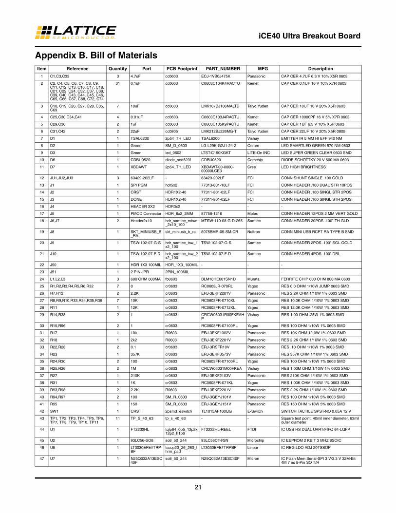
Appendix B. Bill of MaterialsItem Reference Quantity Part PCB Footprint PART_NUMBER MFG Description
1 C1,C3,C33 3 4.7uF cc0603 ECJ-1VB0J475K Panasonic CAP CER 4.7UF 6.3 V 10% X5R 0603
2 C2, C4, C5, C6, C7, C8, C9, C11, C12, C13, C16, C17, C18, C21, C22, C24, C32, C37, C38, C39, C40, C43, C44, C45, C46, C65, C66, C67, C68, C72, C74
31 0.1uF cc0603 C0603C104K4RACTU Kemet CAP CER 0.1UF 16 V 10% X7R 0603
3 C10, C19, C26, C27, C28, C35, C69
7 10uF cc0603 LMK107BJ106MALTD Taiyo Yuden CAP CER 10UF 10 V 20% X5R 0603
4 C25,C30,C34,C41 4 0.01uF cc0603 C0603C103J4RACTU Kemet CAP CER 10000PF 16 V 5% X7R 0603
5 C29,C36 2 1uF cc0603 C0603C105K9PACTU Kemet CAP CER 1UF 6.3 V 10% X5R 0603
6 C31,C42 2 22uF cc0805 LMK212BJ226MG-T Taiyo Yuden CAP CER 22UF 10 V 20% X5R 0805
7 D1 1 TSAL6200 2p54_TH_LED TSAL6200 Vishay EMITTER IR 5 MM HI EFF 940 NM
8 D2 1 Green SM_D_0603 LG L29K-G2J1-24-Z Osram LED SMARTLED GREEN 570 NM 0603
9 D3 1 Green led_0603 LTST-C190KGKT LITE-On INC LED SUPER GREEN CLEAR 0603 SMD
10 D6 1 CDBU0520 diode_sod523f CDBU0520 Comchip DIODE SCHOTTKY 20 V 500 MA 0603
11 D7 1 XBDAWT 2p54_TH_LED XBDAWT-00-0000-00000LCE3
Cree LED HIGH BRIGHTNESS
12 JU1,JU2,JU3 3 63429-202LF - 63429-202LF FCI CONN SHUNT SINGLE .100 GOLD
13 J1 1 SPI PGM hdr5x2 77313-801-10LF FCI CONN HEADER .100 DUAL STR 10POS
14 J2 1 CRST HDR1X2-40 77311-801-02LF FCI CONN HEADER .100 SINGL STR 2POS
15 J3 1 DONE HDR1X2-40 77311-801-02LF FCI CONN HEADER .100 SINGL STR 2POS
16 J4 1 HEADER 3X2 HDR3x2 - - -
17 J5 1 PMOD Connector HDR_6x2_2MM 87758-1216 Molex CONN HEADER 12POS 2 MM VERT GOLD
18 J6,J7 2 Header2x10 hdr_samtec_mtsw_2x10_100
MTSW-110-08-G-D-265 Samtec CONN HEADER 20POS .100" TH GLD
19 J8 1 SKT_MINIUSB_B_RA
skt_miniusb_b_ra 5075BMR-05-SM-CR Neltron CONN MINI USB RCPT RA TYPE B SMD
20 J9 1 TSW-102-07-G-S hdr_samtec_tsw_1x2_100
TSW-102-07-G-S Samtec CONN HEADER 2POS .100" SGL GOLD
21 J10 1 TSW-102-07-F-D hdr_samtec_tsw_2x2_100
TSW-102-07-F-D Samtec CONN HEADER 4POS .100" DBL
22 J50 1 HDR 1X3 100MIL HDR_1X3_100MIL - - -
23 J51 1 2 PIN JPR 2PIN_100MIL - - -
24 L1,L2,L3 3 600 OHM 800MA fb0603 BLM18HE601SN1D Murata FERRITE CHIP 600 OHM 800 MA 0603
25 R1,R2,R3,R4,R5,R6,R32 7 0 cr0603 RC0603JR-070RL Yageo RES 0.0 OHM 1/10W JUMP 0603 SMD
26 R7,R12 2 2.2K cr0603 ERJ-3EKF2201V Panasonic RES 2.2K OHM 1/10W 1% 0603 SMD
27 R8,R9,R10,R33,R34,R35,R36 7 10K cr0603 RC0603FR-0710KL Yageo RES 10.0K OHM 1/10W 1% 0603 SMD
28 R11 1 12K cr0603 RC0603FR-0712KL Yageo RES 12.0K OHM 1/10W 1% 0603 SMD
29 R14,R38 2 1 cr0603 CRCW06031R00FKEAHP
Vishay RES 1.00 OHM .25W 1% 0603 SMD
30 R15,R96 2 1 cr0603 RC0603FR-07100RL Yageo RES 100 OHM 1/10W 1% 0603 SMD
31 R17 1 10k R0603 ERJ-3EKF1002V Panasonic RES 10K OHM 1/10W 1% 0603 SMD
32 R18 1 2k2 R0603 ERJ-3EKF2201V Panasonic RES 2.2K OHM 1/10W 1% 0603 SMD
33 R22,R28 2 0.1 cr0603 ERJ-3RSFR10V Panasonic RES .10 OHM 1/10W 1% 0603 SMD
34 R23 1 357K cr0603 ERJ-3EKF3573V Panasonic RES 357K OHM 1/10W 1% 0603 SMD
35 R24,R30 2 100 cr0603 RC0603FR-07100RL Yageo RES 100 OHM 1/10W 1% 0603 SMD
36 R25,R26 2 1M cr0603 CRCW06031M00FKEA Vishay RES 1.00M OHM 1/10W 1% 0603 SMD
37 R27 1 210K cr0603 ERJ-3EKF2103V Panasonic RES 210K OHM 1/10W 1% 0603 SMD
38 R31 1 1K cr0603 RC0603FR-071KL Yageo RES 1.00K OHM 1/10W 1% 0603 SMD
39 R93,R98 2 2.2K R0603 ERJ-3EKF2201V Panasonic RES 2.2K OHM 1/10W 1% 0603 SMD
40 R94,R97 2 100 SM_R_0603 ERJ-3GEYJ101V Panasonic RES 100 OHM 1/10W 5% 0603 SMD
41 R95 1 150 SM_R_0603 ERJ-3GEYJ151V Panasonic RES 150 OHM 1/10W 5% 0603 SMD
42 SW1 1 CRST 2psmd_eswitch TL1015AF160QG E-Switch SWITCH TACTILE SPST-NO 0.05A 12 V
43 TP1, TP2, TP3, TP4, TP5, TP6, TP7, TP8, TP9, TP10, TP11
11 TP_S_40_63 tp_s_40_63 - - Square test point, 40mil inner diameter, 63mil outer diameter
44 U1 1 FT2232HL tqfp64_0p5_12p2x12p2_h1p6
FT2232HL-REEL FTDI IC USB HS DUAL UART/FIFO 64-LQFP
45 U2 1 93LC56-SO8 so8_50_244 93LC56CT-I/SN Microchip IC EEPROM 2 KBIT 3 MHZ 8SOIC
46 U5 1 LT3030EFE#TRPBF
tssop20_26_260_thrm_pad
LT3030EFE#TRPBF Linear IC REG LDO ADJ 20TSSOP
47 U7 1 N25Q032A13ESC40F
so8_50_244 N25Q032A13ESC40F Micron IC Flash Mem Serial-SPI 3 V/3.3 V 32M-Bit 4M 7 ns 8-Pin SO T/R
22
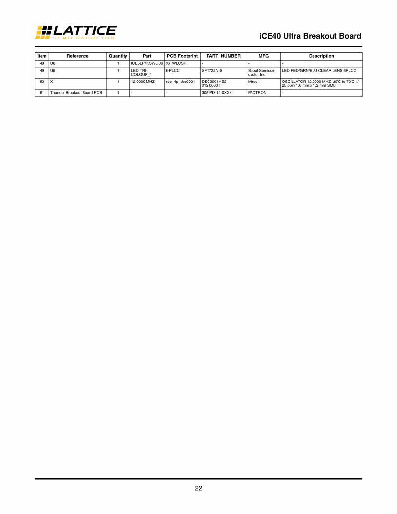
iCE40 Ultra Breakout Board
48 U8 1 ICE5LP4KSWG36 36_WLCSP - - -
49 U9 1 LED TRI-COLOUR_1
6-PLCC SFT722N-S Seoul Semicon-ductor Inc
LED RED/GRN/BLU CLEAR LENS 6PLCC
50 X1 1 12.0000 MHZ osc_4p_dsc3001 DSC3001HE2-012.0000T
Mircel OSCILLATOR 12.0000 MHZ -20'C to 70'C +/-25 ppm 1.6 mm x 1.2 mm SMD
51 Thunder Breakout Board PCB 1 - - 305-PD-14-0XXX PACTRON -
Item Reference Quantity Part PCB Footprint PART_NUMBER MFG Description

![iCE40 UltraLite™ Breakout Board User Guide · RGB Color[3:0] Color Color Code 0000* Red #FF0000 0001 Orange #FF7F00 0010 Yellow #FFFF00 0011 Chartreuse #7FFF00 0100 Green #00FF00](https://img.pdfslide.us/doc/110x75/5fbc0c2323cd28064d5387ce/ice40-ultralitea-breakout-board-user-guide-rgb-color30-color-color-code-0000.jpg)