Embed Size (px)
Citation preview
© 2013 IBM Corporation
IBM Electronic Card Assembly & Test (ECAT) Technology Gap Analysis
Wayne Zhang | Larry Pymento l Matt Kelly | Derek Robertson | Marie Cole ISC Engineering, Global Execution
Aug 2014
IBM Unclassified
ISC Engineering | Global Execution
IBM Unclassified W. Zhang © 2013 IBM Corporation2
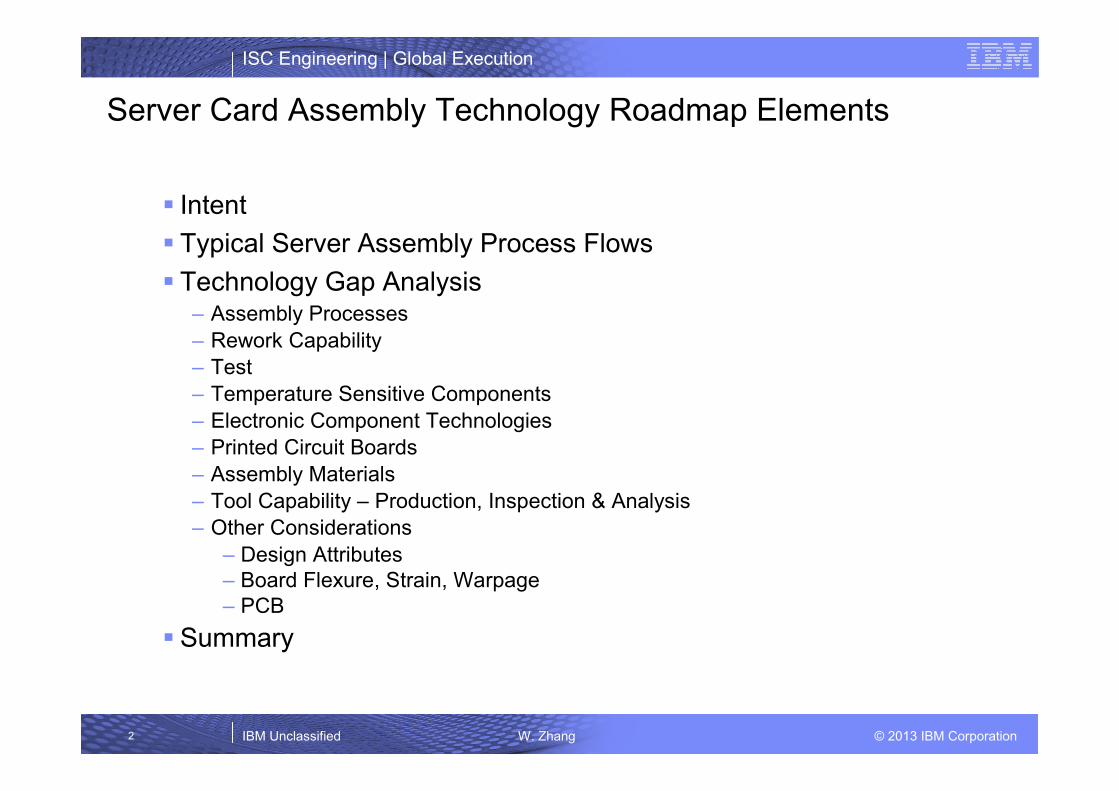
Server Card Assembly Technology Roadmap Elements
� Intent
� Typical Server Assembly Process Flows
� Technology Gap Analysis– Assembly Processes
– Rework Capability
– Test
– Temperature Sensitive Components
– Electronic Component Technologies
– Printed Circuit Boards
– Assembly Materials
– Tool Capability – Production, Inspection & Analysis
– Other Considerations
– Design Attributes
– Board Flexure, Strain, Warpage
– PCB
� Summary
ISC Engineering | Global Execution
IBM Unclassified W. Zhang © 2013 IBM Corporation3
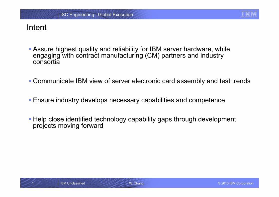
Intent
� Assure highest quality and reliability for IBM server hardware, while engaging with contract manufacturing (CM) partners and industry consortia
�Communicate IBM view of server electronic card assembly and test trends
� Ensure industry develops necessary capabilities and competence
�Help close identified technology capability gaps through development projects moving forward
ISC Engineering | Global Execution
IBM Unclassified W. Zhang © 2013 IBM Corporation4
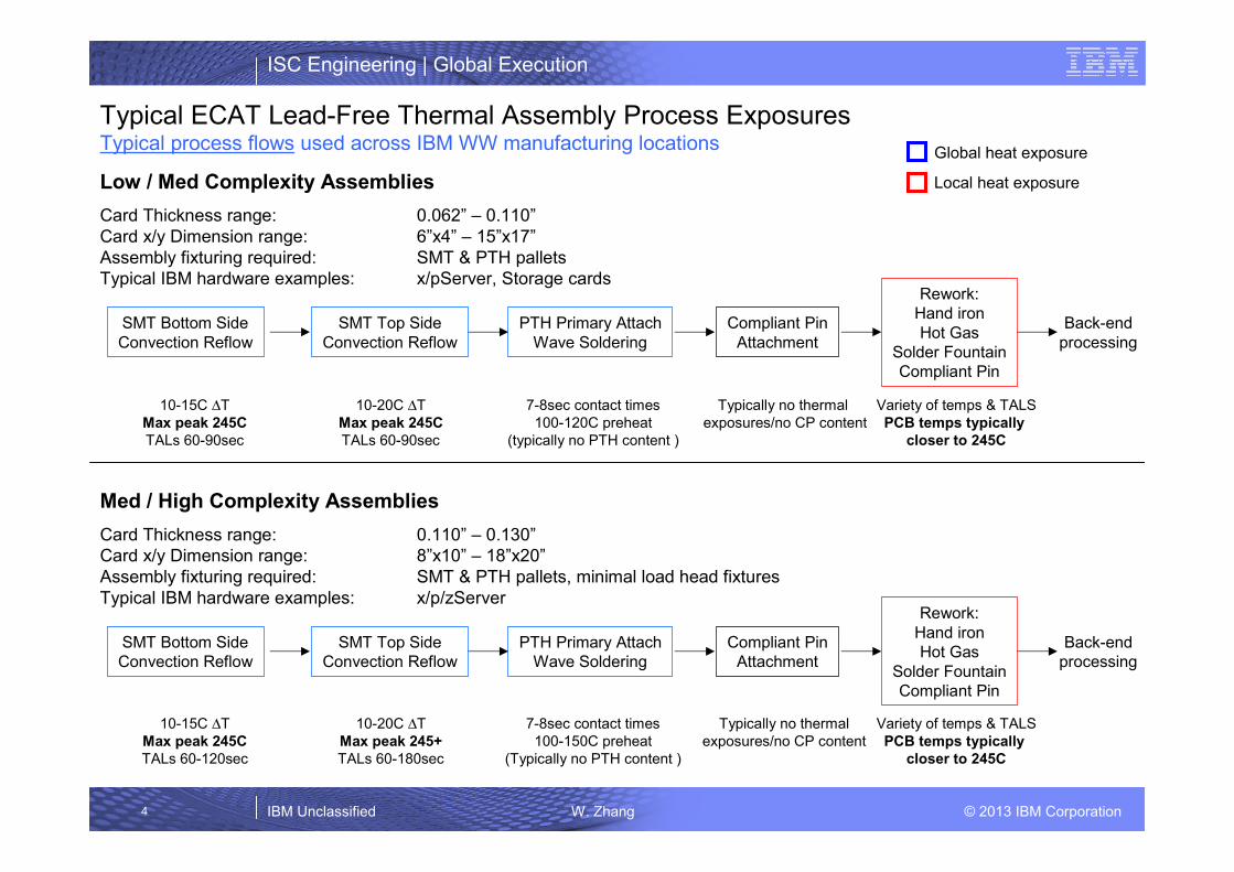
Typical ECAT Lead-Free Thermal Assembly Process ExposuresTypical process flows used across IBM WW manufacturing locations
SMT Bottom Side
Convection Reflow
SMT Top Side
Convection Reflow
PTH Primary Attach
Wave Soldering
10-15C ∆T
Max peak 245C
TALs 60-90sec
10-20C ∆T
Max peak 245C
TALs 60-90sec
Rework:
Hand iron
Hot Gas
Solder Fountain
Compliant Pin
Compliant Pin
Attachment
7-8sec contact times
100-120C preheat
(typically no PTH content )
Variety of temps & TALS
PCB temps typically
closer to 245C
Typically no thermal
exposures/no CP content
Low / Med Complexity Assemblies
Back-end
processing
Card Thickness range: 0.062” – 0.110”
Card x/y Dimension range: 6”x4” – 15”x17”
Assembly fixturing required: SMT & PTH pallets
Typical IBM hardware examples: x/pServer, Storage cards
SMT Bottom Side
Convection Reflow
SMT Top Side
Convection Reflow
PTH Primary Attach
Wave Soldering
10-15C ∆T
Max peak 245C
TALs 60-120sec
10-20C ∆T
Max peak 245+
TALs 60-180sec
Rework:
Hand iron
Hot Gas
Solder Fountain
Compliant Pin
Compliant Pin
Attachment
7-8sec contact times
100-150C preheat
(Typically no PTH content )
Variety of temps & TALS
PCB temps typically
closer to 245C
Typically no thermal
exposures/no CP content
Med / High Complexity Assemblies
Back-end
processing
Card Thickness range: 0.110” – 0.130”
Card x/y Dimension range: 8”x10” – 18”x20”
Assembly fixturing required: SMT & PTH pallets, minimal load head fixtures
Typical IBM hardware examples: x/p/zServer
Global heat exposure
Local heat exposure
ISC Engineering | Global Execution
IBM Unclassified W. Zhang © 2013 IBM Corporation5
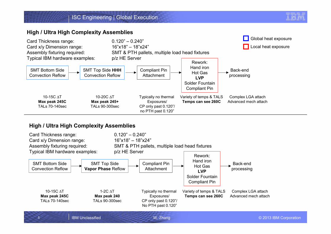
SMT Bottom Side
Convection Reflow
SMT Top Side HHH
Convection Reflow
10-15C ∆T
Max peak 245C
TALs 70-140sec
10-20C ∆T
Max peak 245+
TALs 90-300sec
Rework:
Hand iron
Hot Gas
LVP
Solder Fountain
Compliant Pin
Compliant Pin
Attachment
Variety of temps & TALS
Temps can see 260C
Typically no thermal
Exposures/
CP only past 0.120”/
no PTH past 0.120”
High / Ultra High Complexity Assemblies
Back-end
processing
Card Thickness range: 0.120” – 0.240”
Card x/y Dimension range: 16”x18” – 18”x24”
Assembly fixturing required: SMT & PTH pallets, multiple load head fixtures
Typical IBM hardware examples: p/z HE Server
Complex LGA attach
Advanced mech attach
SMT Bottom Side
Convection Reflow
SMT Top Side
Vapor Phase Reflow
10-15C ∆T
Max peak 245C
TALs 70-140sec
1-2C ∆T
Max peak 240
TALs 90-300sec
Rework:
Hand iron
Hot Gas
LVP
Solder Fountain
Compliant Pin
Compliant Pin
Attachment
Variety of temps & TALS
Temps can see 260C
Typically no thermal
Exposures/
CP only past 0.120”/
No PTH past 0.120”
High / Ultra High Complexity Assemblies
Back-end
processing
Card Thickness range: 0.120” – 0.240”
Card x/y Dimension range: 16”x18” – 18”x24”
Assembly fixturing required: SMT & PTH pallets, multiple load head fixtures
Typical IBM hardware examples: p/z HE Server
Complex LGA attach
Advanced mech attach
Global heat exposure
Local heat exposure
ISC Engineering | Global Execution
IBM Unclassified W. Zhang © 2013 IBM Corporation6
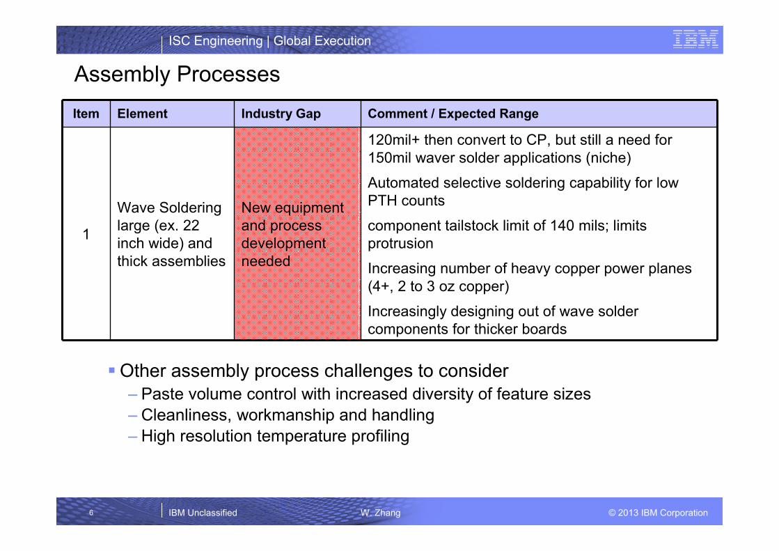
Assembly Processes
New equipment
and process
development
needed
Industry GapItem Element Comment / Expected Range
1
Wave Soldering
large (ex. 22
inch wide) and
thick assemblies
120mil+ then convert to CP, but still a need for
150mil waver solder applications (niche)
Automated selective soldering capability for low
PTH counts
component tailstock limit of 140 mils; limits
protrusion
Increasing number of heavy copper power planes
(4+, 2 to 3 oz copper)
Increasingly designing out of wave solder
components for thicker boards
�Other assembly process challenges to consider
– Paste volume control with increased diversity of feature sizes
– Cleanliness, workmanship and handling
– High resolution temperature profiling
ISC Engineering | Global Execution
IBM Unclassified W. Zhang © 2013 IBM Corporation7
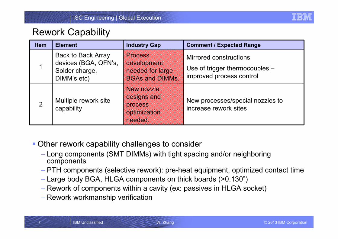
Rework Capability
New nozzle
designs and
process
optimization
needed.
Process
development
needed for large
BGAs and DIMMs.
Industry GapItem Element Comment / Expected Range
1
Back to Back Array
devices (BGA, QFN’s,
Solder charge,
DIMM’s etc)
Mirrored constructions
Use of trigger thermocouples –
improved process control
2Multiple rework site
capability
New processes/special nozzles to
increase rework sites
�Other rework capability challenges to consider
– Long components (SMT DIMMs) with tight spacing and/or neighboring components
– PTH components (selective rework): pre-heat equipment, optimized contact time
– Large body BGA, HLGA components on thick boards (>0.130”)
– Rework of components within a cavity (ex: passives in HLGA socket)
– Rework workmanship verification
ISC Engineering | Global Execution
IBM Unclassified W. Zhang © 2013 IBM Corporation8
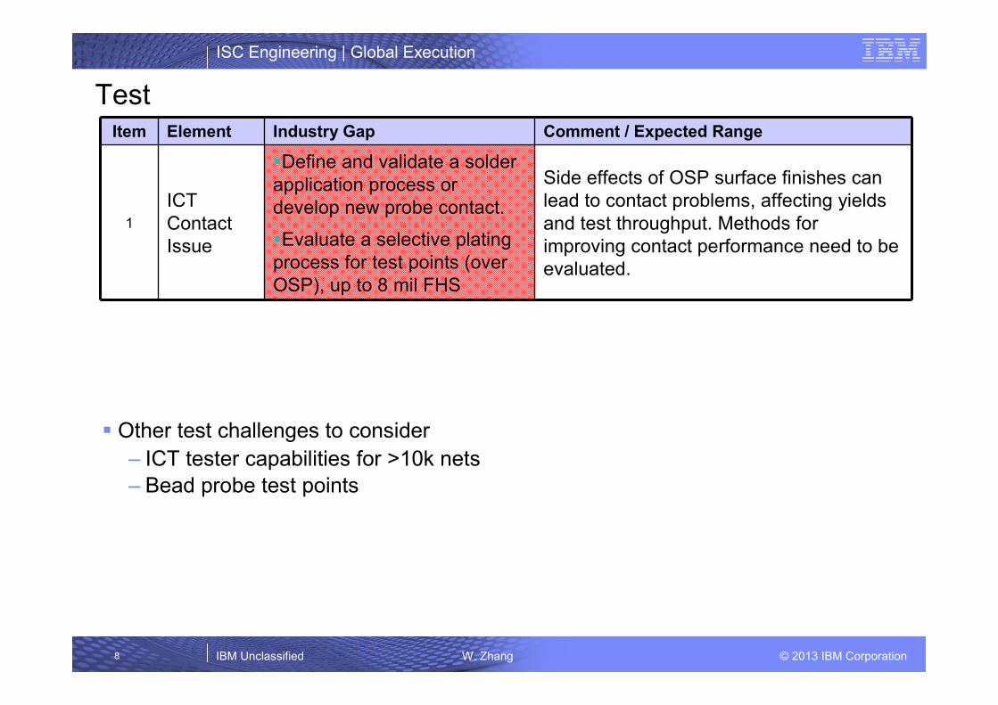
Test
�Define and validate a solder
application process or
develop new probe contact.
�Evaluate a selective plating
process for test points (over
OSP), up to 8 mil FHS
Industry GapItem Element Comment / Expected Range
1
ICT
Contact
Issue
Side effects of OSP surface finishes can
lead to contact problems, affecting yields
and test throughput. Methods for
improving contact performance need to be
evaluated.
� Other test challenges to consider
– ICT tester capabilities for >10k nets
– Bead probe test points
ISC Engineering | Global Execution
IBM Unclassified W. Zhang © 2013 IBM Corporation9
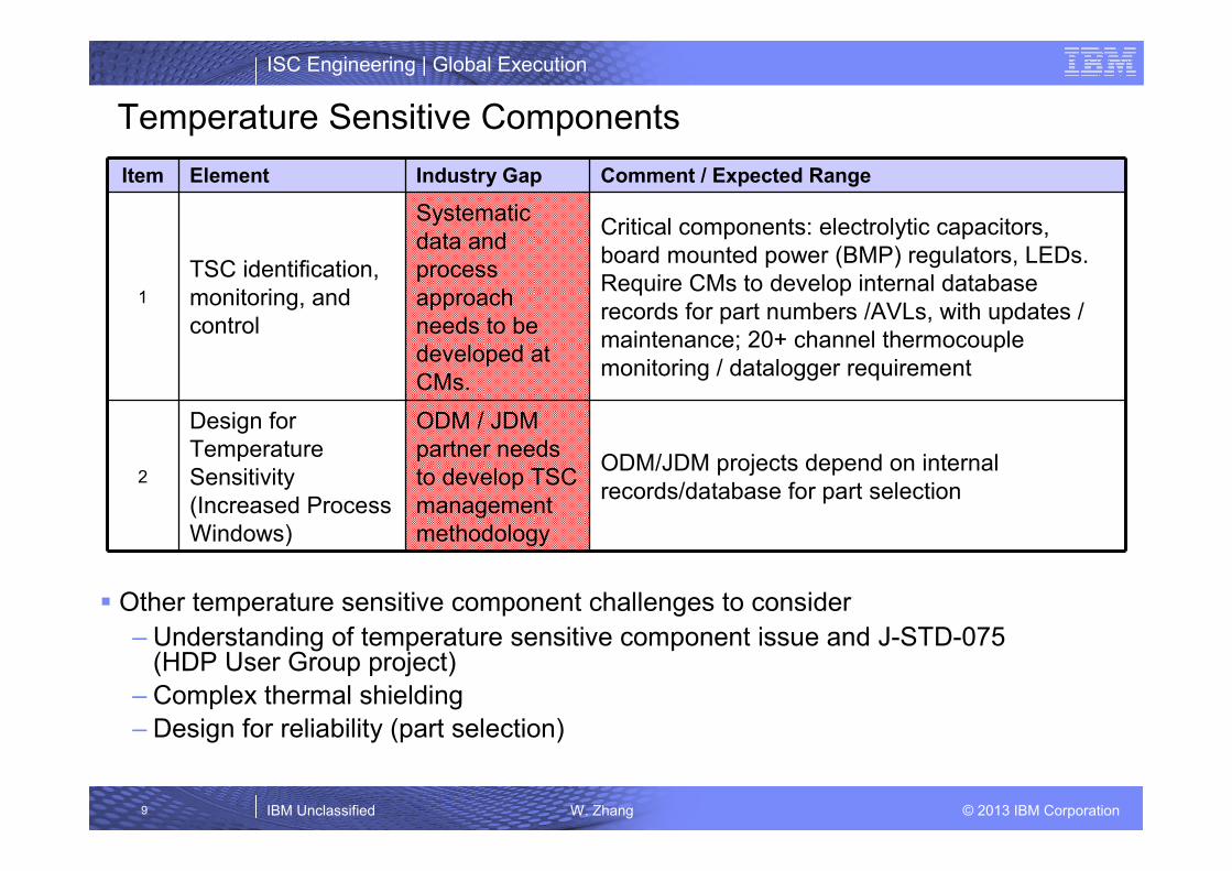
Temperature Sensitive Components
ODM / JDM
partner needs
to develop TSC
management
methodology
Systematic
data and
process
approach
needs to be
developed at
CMs.
Industry GapItem Element Comment / Expected Range
1
TSC identification,
monitoring, and
control
Critical components: electrolytic capacitors,
board mounted power (BMP) regulators, LEDs.
Require CMs to develop internal database
records for part numbers /AVLs, with updates /
maintenance; 20+ channel thermocouple
monitoring / datalogger requirement
2
Design for
Temperature
Sensitivity
(Increased Process
Windows)
ODM/JDM projects depend on internal
records/database for part selection
� Other temperature sensitive component challenges to consider
– Understanding of temperature sensitive component issue and J-STD-075 (HDP User Group project)
– Complex thermal shielding
– Design for reliability (part selection)
ISC Engineering | Global Execution
IBM Unclassified W. Zhang © 2013 IBM Corporation10
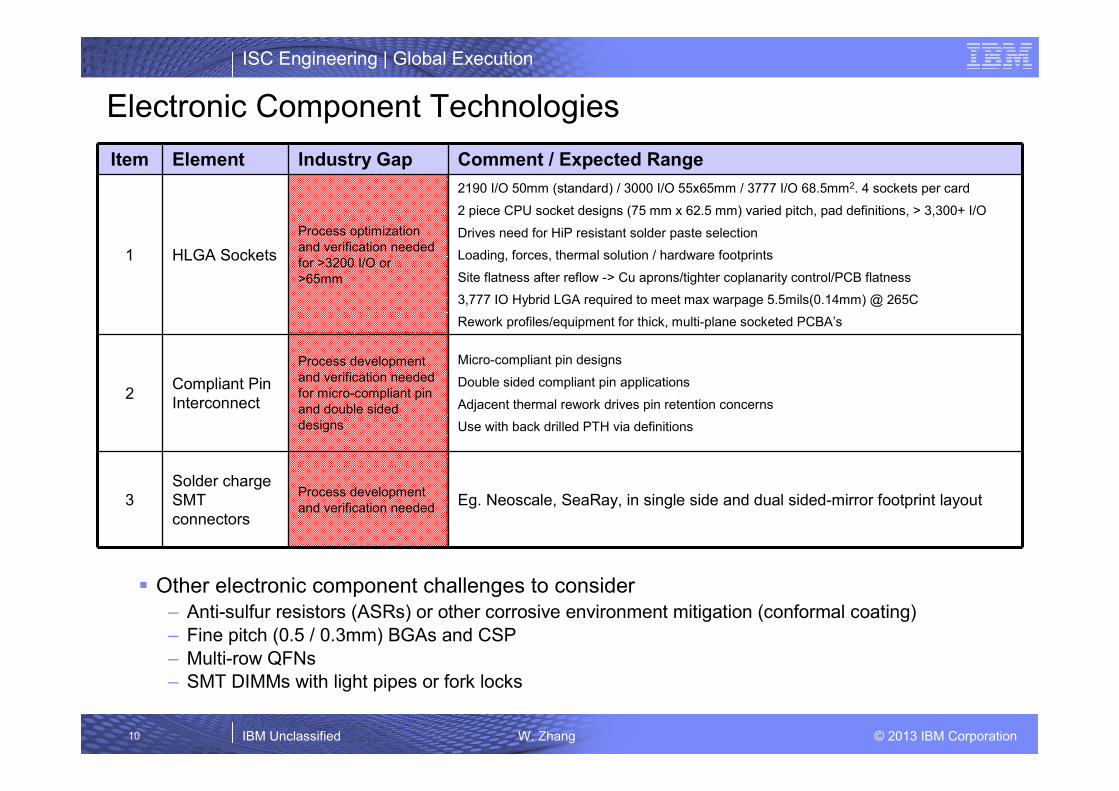
Electronic Component Technologies
Micro-compliant pin designs
Double sided compliant pin applications
Adjacent thermal rework drives pin retention concerns
Use with back drilled PTH via definitions
Process development
and verification needed
for micro-compliant pin
and double sided
designs
Compliant Pin
Interconnect2
2190 I/O 50mm (standard) / 3000 I/O 55x65mm / 3777 I/O 68.5mm2. 4 sockets per card
2 piece CPU socket designs (75 mm x 62.5 mm) varied pitch, pad definitions, > 3,300+ I/O
Drives need for HiP resistant solder paste selection
Loading, forces, thermal solution / hardware footprints
Site flatness after reflow -> Cu aprons/tighter coplanarity control/PCB flatness
3,777 IO Hybrid LGA required to meet max warpage 5.5mils(0.14mm) @ 265C
Rework profiles/equipment for thick, multi-plane socketed PCBA’s
Process optimization
and verification needed
for >3200 I/O or
>65mm
HLGA Sockets1
Process development
and verification needed
Industry GapItem Element Comment / Expected Range
3
Solder charge
SMT
connectors
Eg. Neoscale, SeaRay, in single side and dual sided-mirror footprint layout
� Other electronic component challenges to consider
– Anti-sulfur resistors (ASRs) or other corrosive environment mitigation (conformal coating)
– Fine pitch (0.5 / 0.3mm) BGAs and CSP
– Multi-row QFNs
– SMT DIMMs with light pipes or fork locks
ISC Engineering | Global Execution
IBM Unclassified W. Zhang © 2013 IBM Corporation11
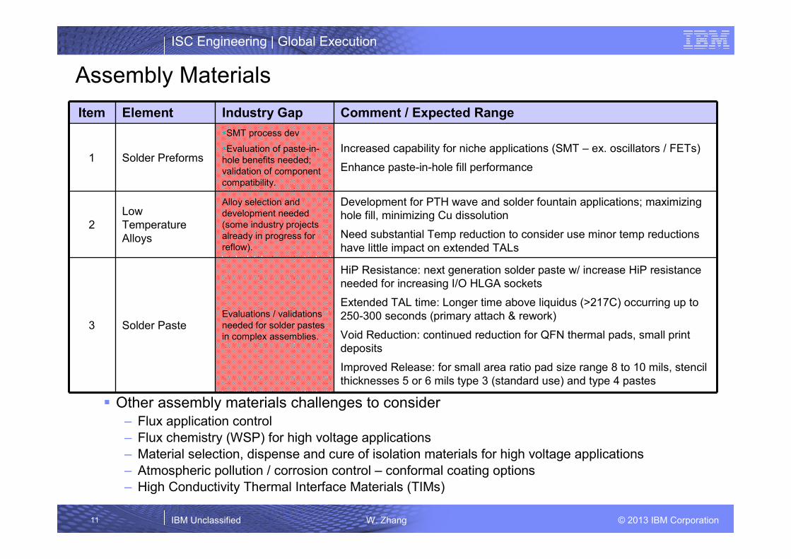
Assembly Materials
Evaluations / validations
needed for solder pastes
in complex assemblies.
Alloy selection and
development needed
(some industry projects
already in progress for
reflow).
�SMT process dev
�Evaluation of paste-in-
hole benefits needed;
validation of component
compatibility.
Industry GapItem Element Comment / Expected Range
1 Solder PreformsIncreased capability for niche applications (SMT – ex. oscillators / FETs)
Enhance paste-in-hole fill performance
2
Low
Temperature
Alloys
Development for PTH wave and solder fountain applications; maximizing
hole fill, minimizing Cu dissolution
Need substantial Temp reduction to consider use minor temp reductions
have little impact on extended TALs
3 Solder Paste
HiP Resistance: next generation solder paste w/ increase HiP resistance
needed for increasing I/O HLGA sockets
Extended TAL time: Longer time above liquidus (>217C) occurring up to
250-300 seconds (primary attach & rework)
Void Reduction: continued reduction for QFN thermal pads, small print
deposits
Improved Release: for small area ratio pad size range 8 to 10 mils, stencil
thicknesses 5 or 6 mils type 3 (standard use) and type 4 pastes
� Other assembly materials challenges to consider
– Flux application control
– Flux chemistry (WSP) for high voltage applications
– Material selection, dispense and cure of isolation materials for high voltage applications
– Atmospheric pollution / corrosion control – conformal coating options
– High Conductivity Thermal Interface Materials (TIMs)
ISC Engineering | Global Execution
IBM Unclassified W. Zhang © 2013 IBM Corporation12
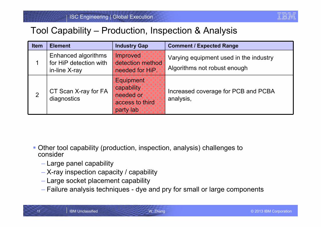
Tool Capability – Production, Inspection & Analysis
Varying equipment used in the industry
Algorithms not robust enough
Improved
detection method
needed for HiP.
Enhanced algorithms
for HiP detection with
in-line X-ray
1
Equipment
capability
needed or
access to third
party lab
Industry GapItem Element Comment / Expected Range
2CT Scan X-ray for FA
diagnostics
Increased coverage for PCB and PCBA
analysis,
� Other tool capability (production, inspection, analysis) challenges to consider
– Large panel capability
– X-ray inspection capacity / capability
– Large socket placement capability
– Failure analysis techniques - dye and pry for small or large components
ISC Engineering | Global Execution
IBM Unclassified W. Zhang © 2013 IBM Corporation13
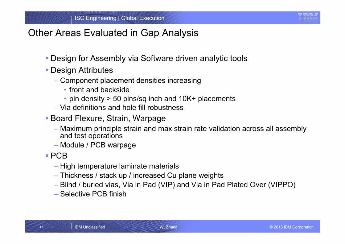
Other Areas Evaluated in Gap Analysis
�Design for Assembly via Software driven analytic tools
�Design Attributes
– Component placement densities increasing
• front and backside
• pin density > 50 pins/sq inch and 10K+ placements
– Via definitions and hole fill robustness
� Board Flexure, Strain, Warpage
– Maximum principle strain and max strain rate validation across all assembly and test operations
– Module / PCB warpage
� PCB
– High temperature laminate materials
– Thickness / stack up / increased Cu plane weights
– Blind / buried vias, Via in Pad (VIP) and Via in Pad Plated Over (VIPPO)
– Selective PCB finish
ISC Engineering | Global Execution
IBM Unclassified W. Zhang © 2013 IBM Corporation14
Summary
� IBM partnering with industry to improve QUALITY
�Extends to PCBA and Test FPY, Box line assembly and Field Performance (Reliability)
� Enabled by Technology Readiness prior to Product Designo Consortia and other Industry Participation (iNEMI, HDPUG, Universal AREA etc.)
o Collaboration with key Technology Partners
o Active test vehicle studies (with product like attributes)
o Roadmap gap analysis – work efforts (IBM/Other OEM’s)
� Enabled by DfX knowledge, Equipment, Process maturity, Material selection and sustained operational procedures/workmanship
ISC Engineering | Global Execution
IBM Unclassified W. Zhang © 2013 IBM Corporation15
Thank you. Questions?
Wayne Zhang, Larry Pymento, Matt Kelly, Marie Cole, Derek Robertson
August 2014