Embed Size (px)
Citation preview
IA80C152 Data Sheet Universal Communications Controller July 29, 2010
IA211040524-06 http://www.Innovasic.com UNCONTROLLED WHEN PRINTED OR COPIED Customer Support: Page 1 of 61 1-888-824-4184
®
IA80C152 Universal Communications Controller Data Sheet
®
IA80C152 Data Sheet Universal Communications Controller July 29, 2010
IA211040524-06 http://www.Innovasic.com UNCONTROLLED WHEN PRINTED OR COPIED Customer Support: Page 2 of 61 1-888-824-4184
®
Copyright 2010 by Innovasic Semiconductor, Inc.
Published by Innovasic Semiconductor, Inc. 3737 Princeton Drive NE, Suite 130, Albuquerque, NM 87107
Intel® is a registered trademark of Intel Corporation. MILES™ is a trademark of Innovasic Semiconductor, Inc.
IA80C152 Data Sheet Universal Communications Controller July 29, 2010
IA211040524-06 http://www.Innovasic.com UNCONTROLLED WHEN PRINTED OR COPIED Customer Support: Page 3 of 61 1-888-824-4184
®
TABLE OF CONTENTS
List of Figures ..................................................................................................................................5 List of Tables ...................................................................................................................................6 1. Introduction .............................................................................................................................7
1.1 General Description .......................................................................................................7 1.2 Features .........................................................................................................................8
2. Packaging, Pin Descriptions, and Physical Dimensions .........................................................9 2.1 Packages and Pinouts ....................................................................................................9
2.1.1 JA/JC...............................................................................................................10 2.1.2 JB/JD...............................................................................................................13
2.1.3 Physical Dimensions .......................................................................................16 2.2 I/O Signal Description .................................................................................................17
3. Maximum Ratings, Thermal Characteristics, and DC Parameters .......................................20
4. Device Architecture ..............................................................................................................22 4.1 Functional Block Diagram ..........................................................................................22
4.2 Memory Space .............................................................................................................23 5. Peripheral Architecture .........................................................................................................25
5.1 Registers and Interrupts ...............................................................................................25
5.2 Register Set Descriptions ............................................................................................27 5.2.1 A* (0E0h) .......................................................................................................27
5.2.2 ADR0,1,2,3 (095h, 0A5h, 0B5h, 0c5h) ..........................................................27 5.2.3 AMSK0,1 (0D5h, 0E5h) .................................................................................28 5.2.4 B* (0F0h) ........................................................................................................28
5.2.5 BAUD (094h) .................................................................................................28
5.2.6 BCRL0, BCRH0 (0E2h, 0E3h) ......................................................................28 5.2.7 BCRL1, BCRH1 (0F2h, 0F3h) .......................................................................28 5.2.8 BKOFF (0C4h) ...............................................................................................28
5.2.9 DARL0, DARH0 (0C2h, 0C3h) .....................................................................28 5.2.10 DARL1, DARH1 (0D2h, 0D3h) .....................................................................29 5.2.11 DCON0,1 (092h, 093h) ..................................................................................29
5.2.12 DPL, DPH (082h, 083h) .................................................................................30 5.2.13 GMOD (084h) ................................................................................................30 5.2.14 IE* (0A8h) ......................................................................................................31 5.2.15 IEN1* (0C8h) .................................................................................................32 5.2.16 IFS (0A4h) ......................................................................................................32
5.2.17 IP* (0B8h) ......................................................................................................33 5.2.18 IPN1* (0F8h) ..................................................................................................33
5.2.19 MYSLOT (0F5h) ............................................................................................34 5.2.20 P0*, P1*, P2*, P3*, P4*, P5, P6 (080h, 090h, 0A0h, 0Boh, 0C0h,
091h, 0A1h) ....................................................................................................34 5.2.21 PCON (087h) ..................................................................................................35 5.2.22 PRBS (0E4h) ..................................................................................................36
IA80C152 Data Sheet Universal Communications Controller July 29, 2010
IA211040524-06 http://www.Innovasic.com UNCONTROLLED WHEN PRINTED OR COPIED Customer Support: Page 4 of 61 1-888-824-4184
®
5.2.23 PSW* (0D0h) ..................................................................................................36 5.2.24 RFIFO (0F4h) .................................................................................................37
5.2.25 RSTAT* (0E8h) ..............................................................................................37 5.2.26 SARL0, SARH0 (0A2h, 0A3h) ......................................................................38 5.2.27 SARL1, SARH1 (0B2h, 0B3h) ......................................................................38 5.2.28 SBUF (099h) ...................................................................................................38 5.2.29 SCON* (098h) ................................................................................................38
5.2.30 SLOTTM (0B4h) ............................................................................................39 5.2.31 SP (081h) ........................................................................................................39 5.2.32 TCDCNT (0D4h) ............................................................................................39 5.2.33 TCON* (088h) ................................................................................................39
5.2.34 TFIFO (085h) ..................................................................................................40 5.2.35 TH0, TL0 (08Ch, 08Ah) .................................................................................40 5.2.36 TH1, TL1 (08Dh, 08Bh) .................................................................................41
5.2.37 TMOD (089h) .................................................................................................41 5.2.38 TSTAT* (0D8h) .............................................................................................41
5.3 Power Conservation Modes ........................................................................................42 5.4 Oscillator Pins .............................................................................................................43
6. Instruction Set Summary Table ............................................................................................50
7. AC Characteristics ................................................................................................................56 8. Innovasic/Intel Part Number Cross-Reference Table ...........................................................57
9. Errata .....................................................................................................................................58 9.1 Errata Summary ...........................................................................................................58 9.2 Errata Detail ................................................................................................................58
10. Revision History ...................................................................................................................60
11. For Additional Information ...................................................................................................61
IA80C152 Data Sheet Universal Communications Controller July 29, 2010
IA211040524-06 http://www.Innovasic.com UNCONTROLLED WHEN PRINTED OR COPIED Customer Support: Page 5 of 61 1-888-824-4184
®
LIST OF FIGURES
Figure 1. JA/JC Versions Package Diagram .................................................................................10
Figure 2. JB/JD Versions Package Diagram .................................................................................13 Figure 3. Package Dimensions ......................................................................................................16 Figure 4. Functional Block Diagram ............................................................................................22 Figure 5. Memory Space ...............................................................................................................24 Figure 6. External Program Memory Read Cycle ........................................................................44
Figure 7. External Data Memory Read Cycle ...............................................................................44 Figure 8. External Data Memory Write Cycle ..............................................................................45 Figure 9. External Clock Drive Waveform ...................................................................................46
Figure 10. Shift Register Mode Timing Waveforms ....................................................................47 Figure 11. GSC Receiver Timings (Internal Baud Rate Generator) .............................................48 Figure 12. GSC Transmit Timings (Internal Baud Rate Generator) .............................................48 Figure 13. GSC Timings (External Clock) ...................................................................................49
IA80C152 Data Sheet Universal Communications Controller July 29, 2010
IA211040524-06 http://www.Innovasic.com UNCONTROLLED WHEN PRINTED OR COPIED Customer Support: Page 6 of 61 1-888-824-4184
®
LIST OF TABLES
Table 1. IC Version Differences .....................................................................................................7
Table 2. JA/JC Versions Numeric Pin Listing ..............................................................................11 Table 3. JA/JC Versions Alphabetic Pin Listing ..........................................................................12 Table 4. JB/JD Versions Numeric Pin Listing ..............................................................................14 Table 5. JB/JD Versions Alphabetic Pin Listing ..........................................................................15 Table 6. I/O Signal Descriptions ...................................................................................................17
Table 7. Absolute Maximum Ratings ...........................................................................................20 Table 8. Thermal Characteristics ..................................................................................................20 Table 9. DC Parameters ................................................................................................................21
Table 10. Summary of Program Memory Fetches ........................................................................25 Table 11. List of Registers ............................................................................................................25 Table 12. List of Interrupts ...........................................................................................................27 Table 13. DCON0,1 Register ........................................................................................................29
Table 14. GMOD Register ............................................................................................................30 Table 15. IE* Register ..................................................................................................................31
Table 16. IEN1* Register .............................................................................................................32 Table 17. IP* Register...................................................................................................................33 Table 18. IPN1* Register ..............................................................................................................33
Table 19. MYSLOT Register ........................................................................................................34 Table 20. P0*, P1*, P2*, P3*, P4*, P5, P6 Register.....................................................................35
Table 21. PCON Register .............................................................................................................35 Table 22. PSW* Register ..............................................................................................................36
Table 23. RSTAT* Register .........................................................................................................37 Table 24. SCON* Register ...........................................................................................................38
Table 25. TCON* Register ...........................................................................................................40 Table 26. TMOD Register ............................................................................................................41 Table 27. TMOD Register ............................................................................................................41
Table 28. Power Conservation Modes ..........................................................................................43 Table 29. External Clock Drive ....................................................................................................46 Table 30. Local Serial Channel Timing—Shift Register Mode ...................................................46
Table 31. Global Serial Port Timing—Internal Baud Rate Generator ..........................................47 Table 32. Global Serial Port Timing—External Clock .................................................................49 Table 33. Instruction Set Summary ..............................................................................................50 Table 34. External Program and Data Memory Characteristics ...................................................56
Table 35. Innovasic/Intel Part Number Cross-Reference .............................................................57 Table 36. Summary of Errata ........................................................................................................58 Table 37. Revision History ...........................................................................................................60
IA80C152 Data Sheet Universal Communications Controller July 29, 2010
IA211040524-06 http://www.Innovasic.com UNCONTROLLED WHEN PRINTED OR COPIED Customer Support: Page 7 of 61 1-888-824-4184
®
1. Introduction
The IA80C152 is a ―plug-and-play‖ drop-in replacement for the original Intel 80C152.
Innovasic produces replacement ICs using its MILES, or Managed IC Lifetime Extension
System, cloning technology. This technology produces replacement ICs far more complex than
―emulation‖ while ensuring they are compatible with the original IC. MILES captures the design
of a clone so it can be produced even as silicon technology advances. MILES also verifies the
clone against the original IC so that even the ―undocumented features‖ are duplicated. This data
sheet presents engineering information about the IA80C152 including functional and I/O
descriptions, electrical characteristics, and applicable timing.
1.1 General Description
The IA80C152 is a Universal Communications Controller (UCC) that is pin-for-pin compatible
with the Intel 80C152. This version of the UCC is a ROM-less version. The ROM version is
identified as the 83C152 and can be easily derived from the 80C152 using a customer furnished
ROM program. The IA80C152 can be programmed with the same software development tools
and can transmit and receive using the same communication protocols as the Intel 80C152
making the IA80C152 a drop-in replacement.
Table 1 below cross-references IA80C152 versions with protocol, package, and I/O Port
capability. Pinout diagrams are provided in Figures 1, 2, and 3.
Table 1. IC Version Differences
Innovasic Part Number
CSMA/CD, SDLC/HDLC, User-Defined
5 I/O Ports
7 I/O Ports
68-Lead PLCC
IA80C152JA
IA80C152JB
IA80C152JC
IA80C152JD
The only difference between The Innovasic IA80C152 and the Intel 80C152 is that all protocols
are available in all IC versions. Originally, the Intel 80C152 JC and JD versions were limited to
SDLC/HDLC only. Also, Innovasic will support a ROM version (83152) in any of the JA, JB,
JC, or JD versions.
Note: If you are using the IA80C152JB/JD in a system that originally used an Intel 80C152JA/JC,
please note that the EBEN pin on the Innovasic part has an internal pull down, so it is recommended
that you do not connect that pin (NC) on your board for proper functionality. In addition, the two
ports that are unused on the JA/JC device (Ports 5 and 6) have internal pullups on the Innovasic
device, so it is recommended that you do not connect (NC) these pins.
IA80C152 Data Sheet Universal Communications Controller July 29, 2010
IA211040524-06 http://www.Innovasic.com UNCONTROLLED WHEN PRINTED OR COPIED Customer Support: Page 8 of 61 1-888-824-4184
®
The IA80C152 is partitioned into three major functional units identified as the C8051, the Direct
Memory Access (DMA) Controller, and the Global Serial Channel (GSC). The C8051 is
implemented using a CAST, Inc. Intellectual Property (IP) core. This core is instruction set
compatible with the 80C51BH, and contains compatible peripherals including a UART interface
and timers. The special function registers (SFRs) and interrupts are modified from the original
8051BH to accommodate the additional DMA controller and GSC peripherals.
The DMA Controller is a 2 channel, 8-bit device that is 16-bit addressable. Either channel can
access any combination of reads and writes to external memory, internal memory, or the SFR's.
Various modes allow the DMA to access the UART, GSC, SFRs, and internal and external
memory as well as provide for external control. Since there is only 1 data/program memory bus,
only one DMA channel or the microcontroller can have control at any given time. Arbitration
within the device makes this control transparent to the programmer.
The GSC is a serial interface that can be programmed to support CSMA/CD, SDLC, user
definable protocols, and limited HDLC. Protocol specific features are supported in hardware
such as address recognition, collision resolution, CRC generation and errors, automatic
re-transmission, and hardware acknowledge. The CSMA/CD protocol meets the requirements of
ISO/IEC 8802-3 and ANSI/IEEE Std 802.3 to the extent implemented in the original IC. The
SDLC protocol meets the requirements of IBM GA27-3093-04 to the extent implemented in the
original IC.
1.2 Features
Form, Fit, and Function Compatible with the Intel 80C152
Packaging options available in both standard and RoHS-Compliant:
– 68-Pin PLCC (plastic leaded chip carrier)
8051 Core with:
– Direct Memory Access (DMA)
– Global Serial Channel (GSC)
– MCS 51-compatible UART
– Two Timers/Counters
– Maskable Interrupts
Memory:
– 256 bytes internal RAM
– 64K bytes program memory
– 64K bytes data memory
5 or 7 I/O Ports
Up to 16.5-MHz Clock Frequency
Two-Channel DMA With Multiple Transfer Modes
GSC Provides Support for Multiple Protocols:
IA80C152 Data Sheet Universal Communications Controller July 29, 2010
IA211040524-06 http://www.Innovasic.com UNCONTROLLED WHEN PRINTED OR COPIED Customer Support: Page 9 of 61 1-888-824-4184
®
– CSMA/CD
– SDLC/HDLC
– User Definable
Separate Transmit & Receive FIFOs
Special Protocol Features:
– Up to 2.0625 Mbps Serial Operation
– CSMA and SDLC Frame Formats with CRC Checking
– Manchester, NRZ, & NRZI Data Encoding
– Collision Detection & Resolution in CSMA Mode
Selectable Full/Half Duplex
2. Packaging, Pin Descriptions, and Physical Dimensions
Information on the packages and pin descriptions is provided in this chapter.
2.1 Packages and Pinouts
The IA80C152 is available in the following packages:
68-Pin PLCC pinout JA/JC versions
68-Pin PLCC pinout JB/JD versions
IA80C152 Data Sheet Universal Communications Controller July 29, 2010
IA211040524-06 http://www.Innovasic.com UNCONTROLLED WHEN PRINTED OR COPIED Customer Support: Page 10 of 61 1-888-824-4184
®
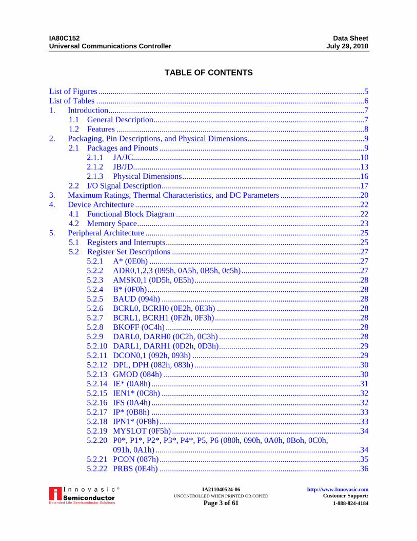
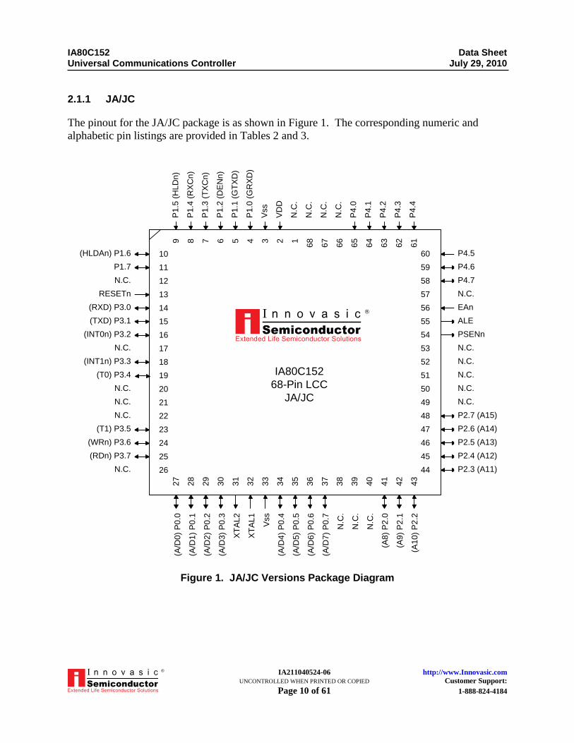
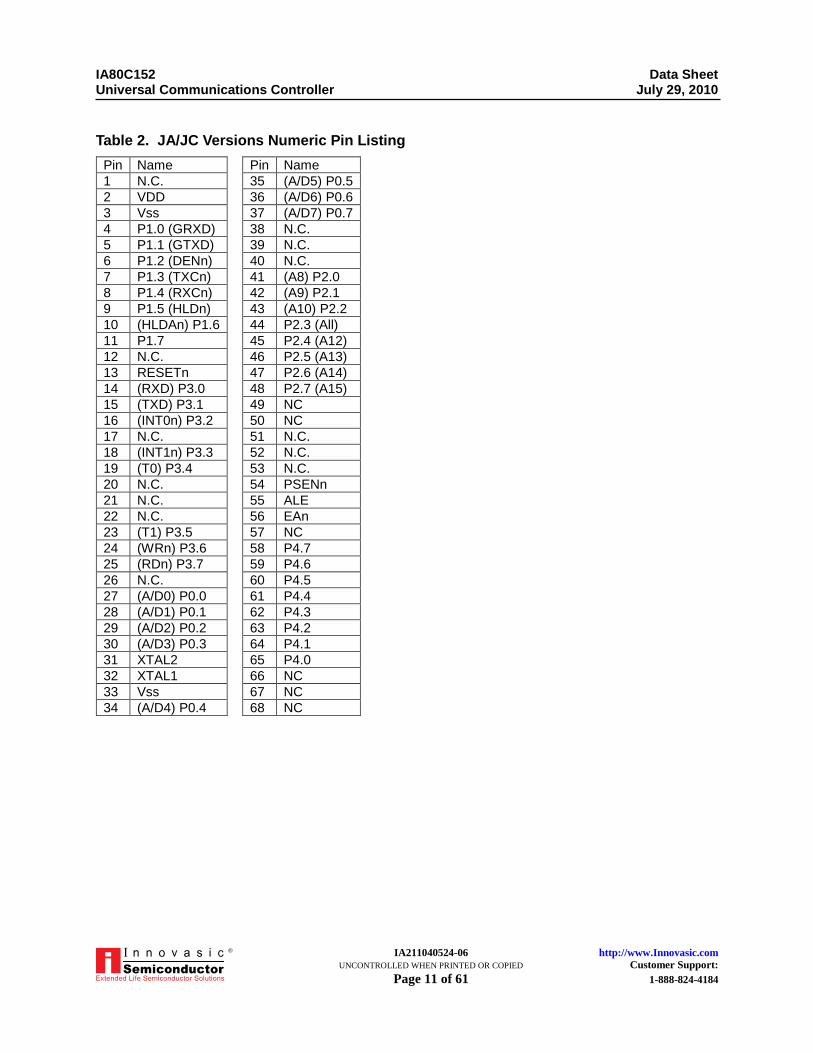
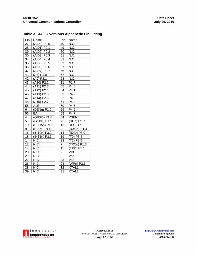
2.1.1 JA/JC
The pinout for the JA/JC package is as shown in Figure 1. The corresponding numeric and
alphabetic pin listings are provided in Tables 2 and 3.
Figure 1. JA/JC Versions Package Diagram
15
10
11
12
13
14
16
17
18
19
20
21
22
23
24
25
26
60
59
58
57
56
55
54
53
52
51
50
49
48
47
46
45
44
32
27
28
29
30
31
33
34
35
36
37
38
39
40
41
42
43
9 8 7 6 5 4 3 2 1
68
67
66
65
64
63
62
61
P4.5
P4.6
P4.7
N.C.
EAn
ALE
PSENn
N.C.
N.C.
N.C.
N.C.
N.C.
P2.7 (A15)
P2.6 (A14)
P2.5 (A13)
P2.4 (A12)
P2.3 (A11)
(A/D
0)
P0
.0
(A/D
1)
P0
.1
(A/D
2)
P0
.2
(A/D
3)
P0
.3
XT
AL
2
XT
AL
1
Vss
(A/D
4)
P0
.4
(A/D
5)
P0
.5
(A/D
6)
P0
.6
(A/D
7)
P0
.7
N.C
.
N.C
.
N.C
.
(A8
) P
2.0
(A9
) P
2.1
(A1
0)
P2
.2
P1.5
(H
LD
n)
P1.4
(R
XC
n)
P1.3
(T
XC
n)
P1.2
(D
EN
n)
P1.1
(G
TX
D)
P1.0
(G
RX
D)
Vss
VD
D
N.C
.
N.C
.
N.C
.
N.C
.
P4.0
P4.1
P4.2
P4.3
P4.4
(HLDAn) P1.6
P1.7
N.C.
RESETn
(RXD) P3.0
(TXD) P3.1
(INT0n) P3.2
N.C.
(INT1n) P3.3
(T0) P3.4
N.C.
N.C.
N.C.
(T1) P3.5
(WRn) P3.6
(RDn) P3.7
N.C.
®
IA80C152
68-Pin LCC
JA/JC
IA80C152 Data Sheet Universal Communications Controller July 29, 2010
IA211040524-06 http://www.Innovasic.com UNCONTROLLED WHEN PRINTED OR COPIED Customer Support: Page 11 of 61 1-888-824-4184
®
Table 2. JA/JC Versions Numeric Pin Listing
Pin Name Pin Name
1 N.C. 35 (A/D5) P0.5
2 VDD 36 (A/D6) P0.6
3 Vss 37 (A/D7) P0.7
4 P1.0 (GRXD) 38 N.C.
5 P1.1 (GTXD) 39 N.C.
6 P1.2 (DENn) 40 N.C.
7 P1.3 (TXCn) 41 (A8) P2.0
8 P1.4 (RXCn) 42 (A9) P2.1
9 P1.5 (HLDn) 43 (A10) P2.2
10 (HLDAn) P1.6 44 P2.3 (All)
11 P1.7 45 P2.4 (A12)
12 N.C. 46 P2.5 (A13)
13 RESETn 47 P2.6 (A14)
14 (RXD) P3.0 48 P2.7 (A15)
15 (TXD) P3.1 49 NC
16 (INT0n) P3.2 50 NC
17 N.C. 51 N.C.
18 (INT1n) P3.3 52 N.C.
19 (T0) P3.4 53 N.C.
20 N.C. 54 PSENn
21 N.C. 55 ALE
22 N.C. 56 EAn
23 (T1) P3.5 57 NC
24 (WRn) P3.6 58 P4.7
25 (RDn) P3.7 59 P4.6
26 N.C. 60 P4.5
27 (A/D0) P0.0 61 P4.4
28 (A/D1) P0.1 62 P4.3
29 (A/D2) P0.2 63 P4.2
30 (A/D3) P0.3 64 P4.1
31 XTAL2 65 P4.0
32 XTAL1 66 NC
33 Vss 67 NC
34 (A/D4) P0.4 68 NC
IA80C152 Data Sheet Universal Communications Controller July 29, 2010
IA211040524-06 http://www.Innovasic.com UNCONTROLLED WHEN PRINTED OR COPIED Customer Support: Page 12 of 61 1-888-824-4184
®
Table 3. JA/JC Versions Alphabetic Pin Listing
Pin Name Pin Name
27 (A/D0) P0.0 40 N.C.
28 (A/D1) P0.1 49 N.C.
29 (A/D2) P0.2 50 N.C.
30 (A/D3) P0.3 51 N.C.
34 (A/D4) P0.4 52 N.C.
35 (A/D5) P0.5 53 N.C.
36 (A/D6) P0.6 57 N.C.
37 (A/D7) P0.7 66 N.C.
41 (A8) P2.0 67 N.C.
42 (A9) P2.1 68 N.C.
43 (A10) P2.2 11 P1.7
44 (A11) P2.3 65 P4.0
45 (A12) P2.4 64 P4.1
46 (A13) P2.5 63 P4.2
47 (A14) P2.6 62 P4.3
48 (A15) P2.7 61 P4.4
55 ALE 60 P4.5
6 (DENn) P1.2 59 P4.6
56 EAn 58 P4.7
4 (GRXD) P1.0 54 PSENn
5 (GTXD) P1.1 25 (RDn) P3.7
10 (HLDAn) P1.6 13 RESETn
9 (HLDn) P1.5 8 (RXCn) P1.4
16 (INT0n) P3.2 14 (RXD) P3.0
18 (INT1n) P3.3 19 (T0) P3.4
1 N.C. 23 (T1) P3.5
12 N.C. 7 (TXCn) P1.3
17 N.C. 15 (TXD) P3.1
20 N.C. 2 VDD
21 N.C. 3 Vss
22 N.C. 33 Vss
26 N.C. 24 (WRn) P3.6
38 N.C. 32 XTAL1
39 N.C. 31 XTAL2
IA80C152 Data Sheet Universal Communications Controller July 29, 2010
IA211040524-06 http://www.Innovasic.com UNCONTROLLED WHEN PRINTED OR COPIED Customer Support: Page 13 of 61 1-888-824-4184
®
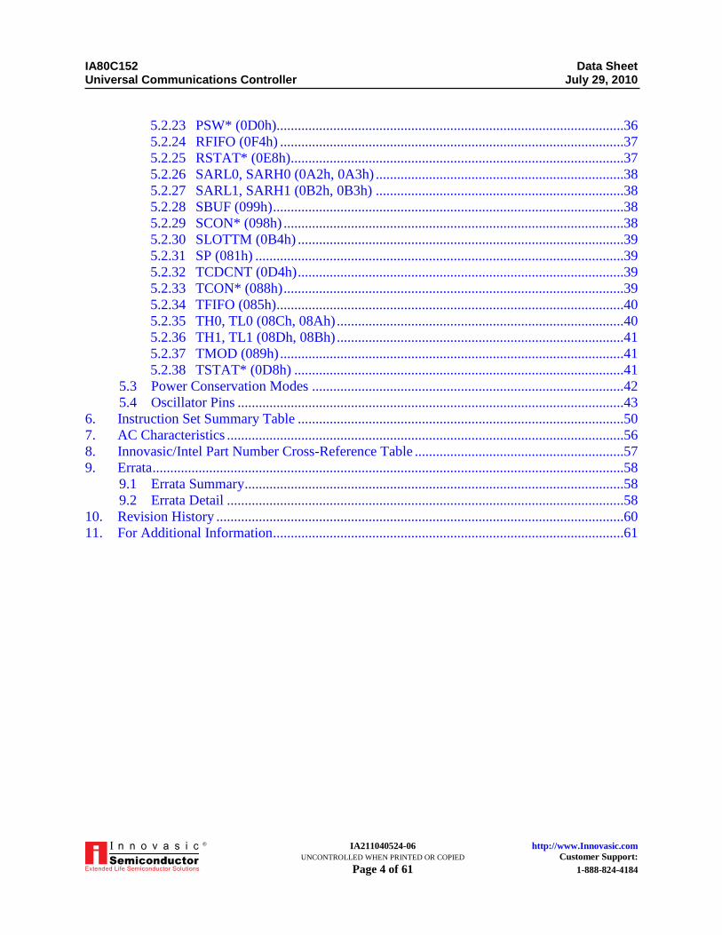
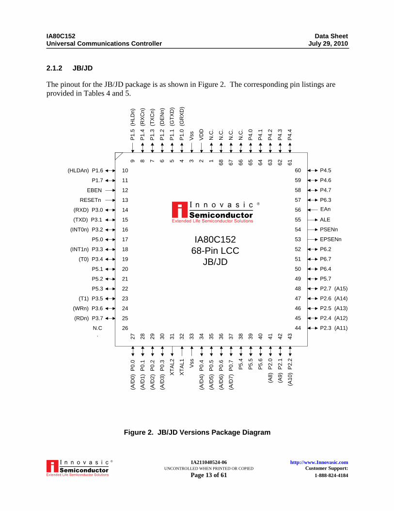
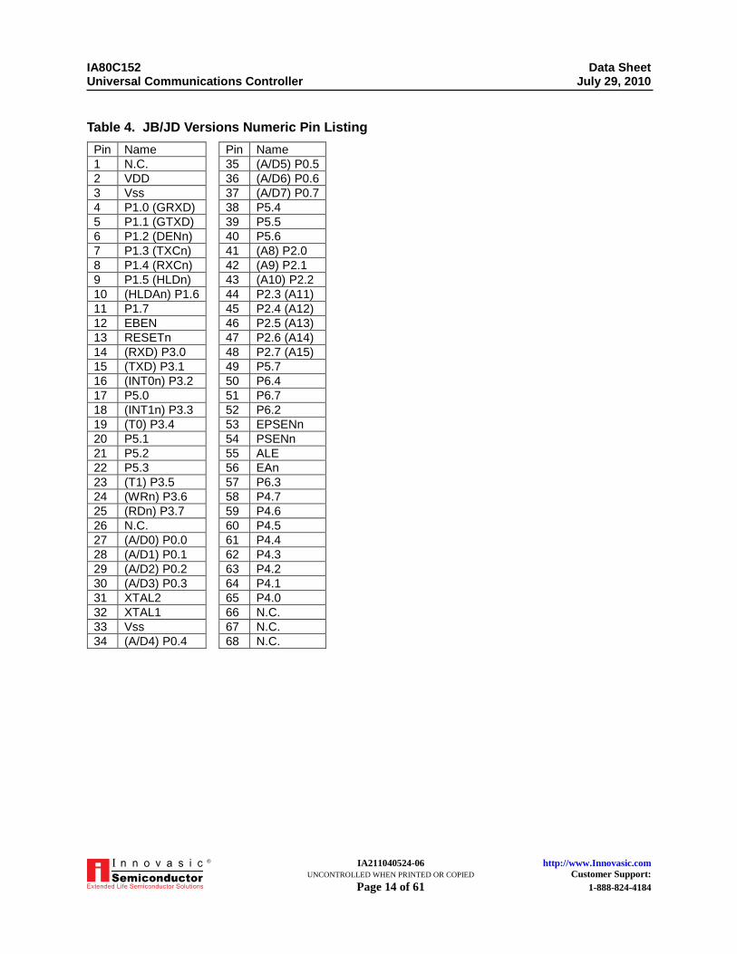
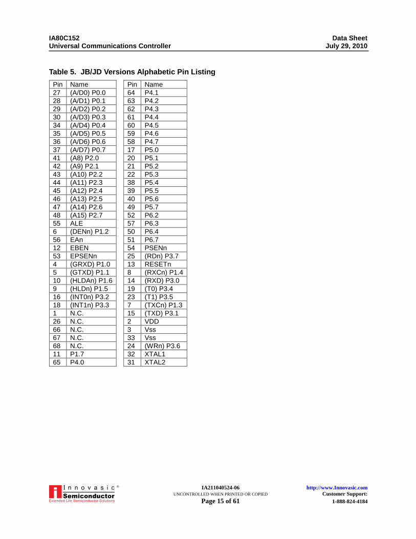
2.1.2 JB/JD
The pinout for the JB/JD package is as shown in Figure 2. The corresponding pin listings are
provided in Tables 4 and 5.
Figure 2. JB/JD Versions Package Diagram
IA80C152
68-Pin LCC
JB/JD
15(TXD) P3.1
10(HLDAn) P1.6
11P1.7
12EBEN
13RESETn
14(RXD) P3.0
16(INT0n) P3.2
17P5.0
18(INT1n) P3.3
19(T0) P3.4
20P5.1
21P5.2
22P5.3
23(T1) P3.5
24(WRn) P3.6
25(RDn) P3.7
26N.C
.
60 P4.5
59
58
57
56
55
54
53
52 P6.2
51 P6.7
50 P6.4
49 P5.7
48 P2.7 (A15)
47 P2.6 (A14)
46
45
44
P2.5 (A13)
P2.4 (A12)
P2.3 (A11)
EPSENn
PSENn
ALE
P6.3
P4.7
P4.63
2X
TA
L1
27
(A/D
0)
P0
.0
28
(A/D
1)
P0
.1
29
(A/D
2)
P0
.2
30
(A/D
3)
P0
.3
31
XT
AL
2
33
Vss
34
(A/D
4)
P0
.4
35
(A/D
5)
P0
.5
36
(A/D
6)
P0
.6
37
(A/D
7)
P0
.7
38
P5
.4
39
P5
.5
40
P5
.6
41
(A8
) P
2.0
42
(A9
) P
2.1
43
(A1
0)
P2
.2
9P
1.5
(H
LD
n)
8 7 6 5 4 3 2 1N
.C.
68
N.C
.
67
N.C
.
66
N.C
.
65
P4
.0
64
P4
.1
63
62
61
P4
.2
P4
.3
P4
.4
VD
D
Vss
P1
.0 (G
RX
D)
P1
.1 (G
TX
D)
P1
.2 (D
EN
n)
P1
.3 (T
XC
n)
P1
.4 (R
XC
n)
EAn®
IA80C152 Data Sheet Universal Communications Controller July 29, 2010
IA211040524-06 http://www.Innovasic.com UNCONTROLLED WHEN PRINTED OR COPIED Customer Support: Page 14 of 61 1-888-824-4184
®
Table 4. JB/JD Versions Numeric Pin Listing
Pin Name Pin Name
1 N.C. 35 (A/D5) P0.5
2 VDD 36 (A/D6) P0.6
3 Vss 37 (A/D7) P0.7
4 P1.0 (GRXD) 38 P5.4
5 P1.1 (GTXD) 39 P5.5
6 P1.2 (DENn) 40 P5.6
7 P1.3 (TXCn) 41 (A8) P2.0
8 P1.4 (RXCn) 42 (A9) P2.1
9 P1.5 (HLDn) 43 (A10) P2.2
10 (HLDAn) P1.6 44 P2.3 (A11)
11 P1.7 45 P2.4 (A12)
12 EBEN 46 P2.5 (A13)
13 RESETn 47 P2.6 (A14)
14 (RXD) P3.0 48 P2.7 (A15)
15 (TXD) P3.1 49 P5.7
16 (INT0n) P3.2 50 P6.4
17 P5.0 51 P6.7
18 (INT1n) P3.3 52 P6.2
19 (T0) P3.4 53 EPSENn
20 P5.1 54 PSENn
21 P5.2 55 ALE
22 P5.3 56 EAn
23 (T1) P3.5 57 P6.3
24 (WRn) P3.6 58 P4.7
25 (RDn) P3.7 59 P4.6
26 N.C. 60 P4.5
27 (A/D0) P0.0 61 P4.4
28 (A/D1) P0.1 62 P4.3
29 (A/D2) P0.2 63 P4.2
30 (A/D3) P0.3 64 P4.1
31 XTAL2 65 P4.0
32 XTAL1 66 N.C.
33 Vss 67 N.C.
34 (A/D4) P0.4 68 N.C.
IA80C152 Data Sheet Universal Communications Controller July 29, 2010
IA211040524-06 http://www.Innovasic.com UNCONTROLLED WHEN PRINTED OR COPIED Customer Support: Page 15 of 61 1-888-824-4184
®
Table 5. JB/JD Versions Alphabetic Pin Listing
Pin Name Pin Name
27 (A/D0) P0.0 64 P4.1
28 (A/D1) P0.1 63 P4.2
29 (A/D2) P0.2 62 P4.3
30 (A/D3) P0.3 61 P4.4
34 (A/D4) P0.4 60 P4.5
35 (A/D5) P0.5 59 P4.6
36 (A/D6) P0.6 58 P4.7
37 (A/D7) P0.7 17 P5.0
41 (A8) P2.0 20 P5.1
42 (A9) P2.1 21 P5.2
43 (A10) P2.2 22 P5.3
44 (A11) P2.3 38 P5.4
45 (A12) P2.4 39 P5.5
46 (A13) P2.5 40 P5.6
47 (A14) P2.6 49 P5.7
48 (A15) P2.7 52 P6.2
55 ALE 57 P6.3
6 (DENn) P1.2 50 P6.4
56 EAn 51 P6.7
12 EBEN 54 PSENn
53 EPSENn 25 (RDn) P3.7
4 (GRXD) P1.0 13 RESETn
5 (GTXD) P1.1 8 (RXCn) P1.4
10 (HLDAn) P1.6 14 (RXD) P3.0
9 (HLDn) P1.5 19 (T0) P3.4
16 (INT0n) P3.2 23 (T1) P3.5
18 (INT1n) P3.3 7 (TXCn) P1.3
1 N.C. 15 (TXD) P3.1
26 N.C. 2 VDD
66 N.C. 3 Vss
67 N.C. 33 Vss
68 N.C. 24 (WRn) P3.6
11 P1.7 32 XTAL1
65 P4.0 31 XTAL2
IA80C152 Data Sheet Universal Communications Controller July 29, 2010
IA211040524-06 http://www.Innovasic.com UNCONTROLLED WHEN PRINTED OR COPIED Customer Support: Page 16 of 61 1-888-824-4184
®
.10
.51 MIN.
R 1.14 / .64
SEATING PLANE
A1
e
.81 / .66
A
.53 / .33
D2 / E2
SIDE VIEW
D3
E3
PIN 1
IDENTIFIER & ZONE
1.2
2/1
.07
2 P
LC
S
TOP VIEW
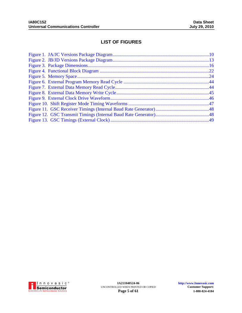
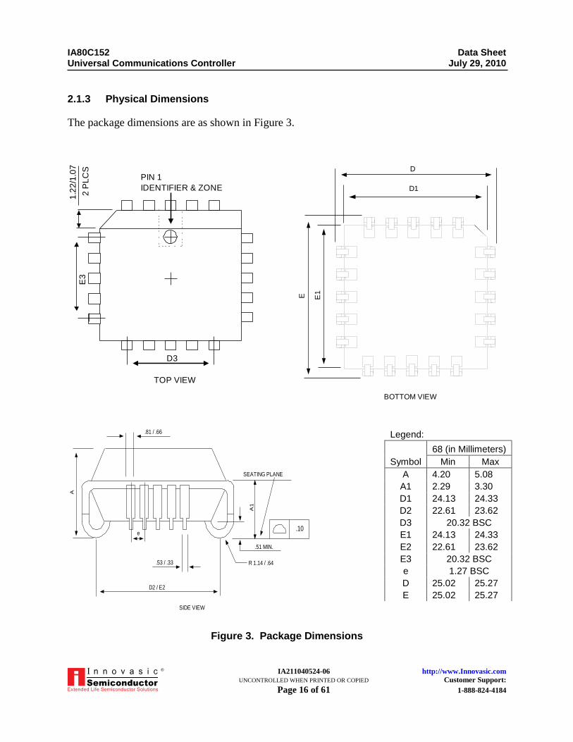
2.1.3 Physical Dimensions
The package dimensions are as shown in Figure 3.
Figure 3. Package Dimensions
Legend:
Symbol
68 (in Millimeters)
Min Max
A 4.20 5.08
A1 2.29 3.30
D1 24.13 24.33
D2 22.61 23.62
D3 20.32 BSC
E1 24.13 24.33
E2 22.61 23.62
E3 20.32 BSC
e 1.27 BSC
D 25.02 25.27
E 25.02 25.27
D
D1
E E1
BOTTOM VIEW
IA80C152 Data Sheet Universal Communications Controller July 29, 2010
IA211040524-06 http://www.Innovasic.com UNCONTROLLED WHEN PRINTED OR COPIED Customer Support: Page 17 of 61 1-888-824-4184
®
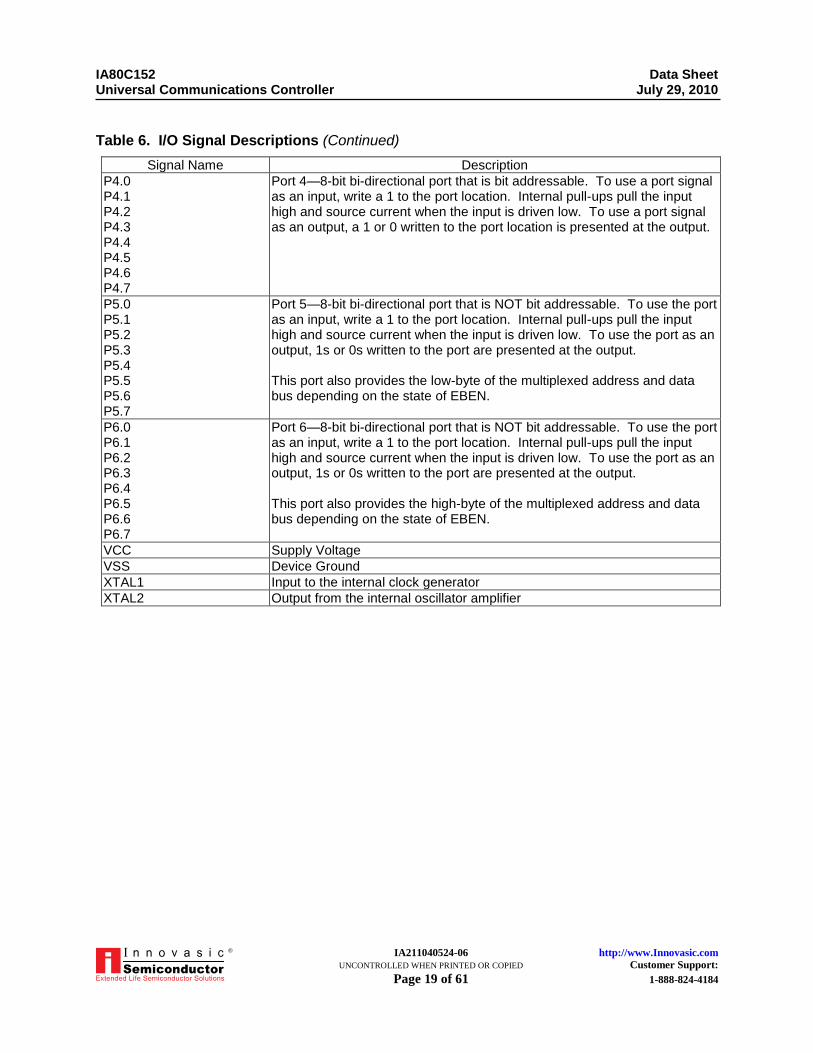
2.2 I/O Signal Description
Table 6 below describes the I/O characteristics for each signal on the IC. The signal names
correspond to the signal names on the pinout diagrams provided above. The (n) denotes active
low.
Table 6. I/O Signal Descriptions
Signal Name Description
EAn External Access enable. Since there is no internal ROM in the IA80C152, this signal has no function in the JA and JC versions and should be set to 0. For the JB and JD versions with EBEN, it controls program memory fetches from ports 0, 2 or ports 5, 6. See Table 3.
EPSENn E-bus Program Store ENable. When EBEN is 1, this signal is the read strobe for external program memory. JB/JD versions only.
PSENn Program Store ENable. When EBEN is 0, this signal is the read strobe for external program memory.
RESETn Reset. When this signal is low for 3 machine cycles, the device is put into reset. The GSC may continue transmitting after reset is applied. An internal pull-up allows the use of an external capacitor to generate a power-on reset.
ALE Address Latch Enable. Latches the low-byte of external memory.
EBEN E-Bus ENable. In conjunction with EAn, EBEN designates program memory fetches from either Port 0,2 or Port 5,6. See Table 3.
P0.0 P0.1 P0.2 P0.3 P0.4 P0.5 P0.6 P0.7
Port 0 - open drain 8-bit bi-directional port that is bit addressable and can drive up to 8 LS TTL inputs. The port signals can be used as high impedance inputs. This port also provides the low-byte of the multiplexed address and data bus depending on the state of EBEN.
IA80C152 Data Sheet Universal Communications Controller July 29, 2010
IA211040524-06 http://www.Innovasic.com UNCONTROLLED WHEN PRINTED OR COPIED Customer Support: Page 18 of 61 1-888-824-4184
®
Table 6. I/O Signal Descriptions (Continued)
Signal Name Description
P1.0 - GRXD, GSC Receive P1.1 - GTXD, GSC Transmit P1.2 - DENn, Driver Enable P1.3 - TXCn, External Transmit Clock P1.4 - RXCn, External Receive Clock P1.5 - HLDn, DMA Hold P1.6 - HLDAn, DMA Hold Acknowledge P1.7
Port 1—8-bit bi-directional port that is bit addressable. To use a port signal as an input, write a 1 to the port location. Internal pull-ups pull the input high and source current when the input is driven low. To use a port signal as an output, a 1 or 0 written to the port location is presented at the output. Port signals in this port also serve as I/O for IA80C152 functions. These I/O signals are defined next to the port name.
P2.0 P2.1 P2.2 P2.3 P2.4 P2.5 P2.6 P2.7
Port 2—8-bit bi-directional port that is bit addressable. To use a port signal as an input, write a 1 to the port location. Internal pull-ups pull the input high and source current when the input is driven low. To use a port signal as an output, a 1 or 0 written to the port location is presented at the output. This port also provides the high-byte of the multiplexed address and data bus depending on the state of EBEN.
P3.0 - RXD, UART Receive P3.1 - TXD, UART Transmit P3.2 - INT0n, External Interrupt 0 P3.3 - INT1n, External Interrupt 1 P3.4 - T0, Timer 0 External Input P3.5 - T1, Timer 1 External Input P3.6 - WRn, External Data Memory Write Strobe P3.7 - RDn, External Data Memory Read Strobe
Port 3—8-bit bi-directional port that is bit addressable. To use a port signal as an input, write a 1 to the port location. Internal pull-ups pull the input high and source current when the input is driven low. To use a port signal as an output, a 1 or 0 written to the port location is presented at the output. Port signals in this port also serve as I/O for IA80C152 functions. These I/O signals are defined next to the port name.
IA80C152 Data Sheet Universal Communications Controller July 29, 2010
IA211040524-06 http://www.Innovasic.com UNCONTROLLED WHEN PRINTED OR COPIED Customer Support: Page 19 of 61 1-888-824-4184
®
Table 6. I/O Signal Descriptions (Continued)
Signal Name Description
P4.0 P4.1 P4.2 P4.3 P4.4 P4.5 P4.6 P4.7
Port 4—8-bit bi-directional port that is bit addressable. To use a port signal as an input, write a 1 to the port location. Internal pull-ups pull the input high and source current when the input is driven low. To use a port signal as an output, a 1 or 0 written to the port location is presented at the output.
P5.0 P5.1 P5.2 P5.3 P5.4 P5.5 P5.6 P5.7
Port 5—8-bit bi-directional port that is NOT bit addressable. To use the port as an input, write a 1 to the port location. Internal pull-ups pull the input high and source current when the input is driven low. To use the port as an output, 1s or 0s written to the port are presented at the output. This port also provides the low-byte of the multiplexed address and data bus depending on the state of EBEN.
P6.0 P6.1 P6.2 P6.3 P6.4 P6.5 P6.6 P6.7
Port 6—8-bit bi-directional port that is NOT bit addressable. To use the port as an input, write a 1 to the port location. Internal pull-ups pull the input high and source current when the input is driven low. To use the port as an output, 1s or 0s written to the port are presented at the output. This port also provides the high-byte of the multiplexed address and data bus depending on the state of EBEN.
VCC Supply Voltage
VSS Device Ground
XTAL1 Input to the internal clock generator
XTAL2 Output from the internal oscillator amplifier
IA80C152 Data Sheet Universal Communications Controller July 29, 2010
IA211040524-06 http://www.Innovasic.com UNCONTROLLED WHEN PRINTED OR COPIED Customer Support: Page 20 of 61 1-888-824-4184
®
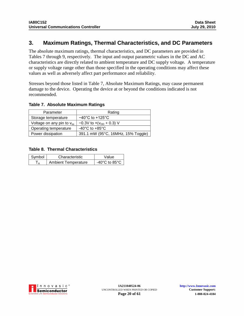
3. Maximum Ratings, Thermal Characteristics, and DC Parameters
The absolute maximum ratings, thermal characteristics, and DC parameters are provided in
Tables 7 through 9, respectively. The input and output parametric values in the DC and AC
characteristics are directly related to ambient temperature and DC supply voltage. A temperature
or supply voltage range other than those specified in the operating conditions may affect these
values as well as adversely affect part performance and reliability.
Stresses beyond those listed in Table 7, Absolute Maximum Ratings, may cause permanent
damage to the device. Operating the device at or beyond the conditions indicated is not
recommended.
Table 7. Absolute Maximum Ratings
Parameter Rating
Storage temperature −40°C to +125°C
Voltage on any pin to vss −0.3V to +(vDD + 0.3) V
Operating temperature -40°C to +85°C
Power dissipation 391.1 mW (95°C, 16MHz, 15% Toggle)
Table 8. Thermal Characteristics
Symbol Characteristic Value
TA Ambient Temperature -40°C to 85°C
IA80C152 Data Sheet Universal Communications Controller July 29, 2010
IA211040524-06 http://www.Innovasic.com UNCONTROLLED WHEN PRINTED OR COPIED Customer Support: Page 21 of 61 1-888-824-4184
®
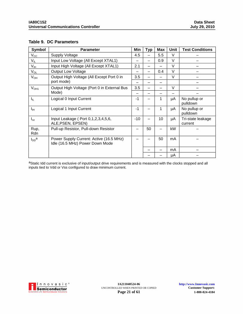
Table 9. DC Parameters
Symbol Parameter Min Typ Max Unit Test Conditions
VCC Supply Voltage 4.5 – 5.5 V –
VIL Input Low Voltage (All Except XTAL1) – – 0.9 V –
VIH Input High Voltage (All Except XTAL1) 2.1 – – V –
VOL Output Low Voltage – – 0.4 V –
VOH Output High Voltage (All Except Port 0 in port mode)
3.5 – – V –
– – – –
VOH1 Output High Voltage (Port 0 in External Bus Mode)
3.5 – – V –
– – – – –
IIL Logical 0 Input Current -1 – 1 µA No pullup or pulldown
IIH Logical 1 Input Current -1 – 1 µA No pullup or pulldown
Ioz Input Leakage ( Port 0,1,2,3,4,5,6, ALE,PSEN, EPSEN)
-10 – 10 µA Tri-state leakage current
Rup, Rdn
Pull-up Resistor, Pull-down Resistor – 50 – kW –
IDDa Power Supply Current: Active (16.5 MHz)
Idle (16.5 MHz) Power Down Mode – – 50 mA –
– – mA –
– – µA –
aStatic Idd current is exclusive of input/output drive requirements and is measured with the clocks stopped and all inputs tied to Vdd or Vss configured to draw minimum current.
IA80C152 Data Sheet Universal Communications Controller July 29, 2010
IA211040524-06 http://www.Innovasic.com UNCONTROLLED WHEN PRINTED OR COPIED Customer Support: Page 22 of 61 1-888-824-4184
®
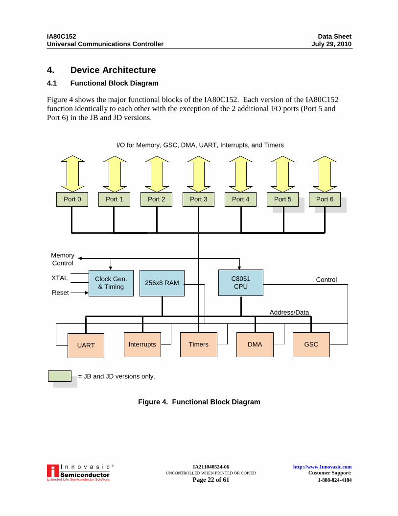
4. Device Architecture
4.1 Functional Block Diagram
Figure 4 shows the major functional blocks of the IA80C152. Each version of the IA80C152
function identically to each other with the exception of the 2 additional I/O ports (Port 5 and
Port 6) in the JB and JD versions.
Figure 4. Functional Block Diagram
Port 3Port 2Port 1Port 0
256x8 RAMControlXTAL
Reset
I/O for Memory, GSC, DMA, UART, Interrupts, and Timers
Clock Gen.
& Timing
C8051
CPU
UART
Address/Data
Memory
Control
Port 4 Port 5 Port 6
Interrupts Timers DMA GSC
= JB and JD versions only.
IA80C152 Data Sheet Universal Communications Controller July 29, 2010
IA211040524-06 http://www.Innovasic.com UNCONTROLLED WHEN PRINTED OR COPIED Customer Support: Page 23 of 61 1-888-824-4184
®
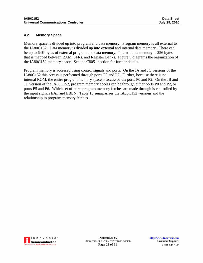
4.2 Memory Space
Memory space is divided up into program and data memory. Program memory is all external to
the IA80C152. Data memory is divided up into external and internal data memory. There can
be up to 64K bytes of external program and data memory. Internal data memory is 256 bytes
that is mapped between RAM, SFRs, and Register Banks. Figure 5 diagrams the organization of
the IA80C152 memory space. See the C8051 section for further details.
Program memory is accessed using control signals and ports. On the JA and JC versions of the
IA80C152 this access is performed through ports P0 and P2. Further, because there is no
internal ROM, the entire program memory space is accessed via ports P0 and P2. On the JB and
JD version of the IA80C152, program memory access can be through either ports P0 and P2, or
ports P5 and P6. Which set of ports program memory fetches are made through is controlled by
the input signals EAn and EBEN. Table 10 summarizes the IA80C152 versions and the
relationship to program memory fetches.
IA80C152 Data Sheet Universal Communications Controller July 29, 2010
IA211040524-06 http://www.Innovasic.com UNCONTROLLED WHEN PRINTED OR COPIED Customer Support: Page 24 of 61 1-888-824-4184
®
Figure 5. Memory Space
Upper
128 Bytes
External RAM
SFR Space
Lower
128 Bytes
Internal RAM
FFFFH
C000H
8000H
4000H
0000H
FFH
80H
7FH
00H
IA80C152 Data Sheet Universal Communications Controller July 29, 2010
IA211040524-06 http://www.Innovasic.com UNCONTROLLED WHEN PRINTED OR COPIED Customer Support: Page 25 of 61 1-888-824-4184
®
Table 10. Summary of Program Memory Fetches
Version
Fetch Control
Fetch Ports
Fetch Signal
Memory Space EBEN EAn PSENn EPSENn
JA, JC NA 0 or 1 P0, P2 Active – 0h–FFFFh
JB, JD 0 0 P0, P2 Active – 0h–FFFFh
1 0 P5, P6 – Active 0h–FFFFh
1 1 P5, P6 – Active 0h–1FFFh
P0, P2 Active – 2000h–FFFFh
5. Peripheral Architecture
5.1 Registers and Interrupts
The IA80C152 combines the register set of the 8051BH and additional SFRs for the DMA and
GSC functions. Likewise, the IA80C152 combines the interrupts of the 8051BH and the
interrupts required by the DMA and GSC. Tables 11 and 12 list the IA80C152 registers
interrupts, respectively.
Table 11. List of Registers
Item Register Name
Register Address
Functional Block Description
Initial Value
1 A 0E0h C8051 Accumulator 00h
2 ADR0 095h GSC Address Match 0 00h
3 ADR1 0A5h GSC Address Match 1 00h
4 ADR2 0B5h GSC Address Match 2 00h
5 ADR3 0C5h GSC Address Match 3 00h
6 AMSK0 0D5h GSC Address Mask 0 00h
7 AMSK1 0E5h GSC Address Mask 1 00h
8 B 0F0h C8051 B Register 00h
9 BAUD 094h GSC Baud Rate 00h
10 BCRL0 0E2h DMA Byte Count Register (Low) 0 X
11 BCRH0 0E3h DMA Byte Count Register (High) 0 X
12 BCRL1 0F2h DMA Byte Count Register (Low) 1 X
13 BCRH1 0F3h DMA Byte Count Register (High) 1 X
14 BKOFF 0C4h GSC Backoff Timer X
15 DARL0 0C2h DMA Destination Address Register (Low) 0 X
16 DARH0 0C3h DMA Destination Address Register (High) 0 X
17 DARL1 0D2h DMA Destination Address Register (Low) 1 X
18 DARH1 0D3h DMA Destination Address Register (High) 1 X
19 DCON0 092h DMA DMA Control 0 00h
20 DCON1 093h DMA DMA Control 1 00h
21 DPH 083h C8051 Data Pointer High 00h
22 DPL 082h C8051 Data Pointer Low 00h
23 GMOD 084h GSC GSC Mode X0000000b
24 IE 0A8h C8051 Interrupt Enable 0XX00000b
25 IEN1 0C8h DMA, GSC Interrupt Enable 1 XX000000b
IA80C152 Data Sheet Universal Communications Controller July 29, 2010
IA211040524-06 http://www.Innovasic.com UNCONTROLLED WHEN PRINTED OR COPIED Customer Support: Page 26 of 61 1-888-824-4184
®
Table 11. List of Registers (Continued)
Item Register Name
Register Address
Functional Block
Description Initial Value
26 IFS 0A4h GSC Interframe Space 00h
27 IP 0B8h C8051 Interrupt Priority XXX00000b
28 IPN1 0F8h DMA, GSC Interrupt Priority 1 XX000000b
29 MYSLOT 0F5h GSC GSC Slot Address 00h
30 P0 080h C8051 Port 0 0FFh
31 P1 090h C8051 Port 1 0FFh
32 P2 0A0h C8051 Port 2 0FFh
33 P3 0B0h C8051 Port 3 0FFh
34 P4 0C0h C8051 Port 4 0FFh
35 P5 091h C8051 Port 5 0FFh
36 P6 0A1h C8051 Port 6 0FFh
37 PCON 087h C8051 Power Control 0XXX0000b
38 PRBS 0E4h GSC Pseudo-Random Sequence 00h
39 PSW 0D0h C8051 Program Status Word 00h
40 RFIFO 0F4h GSC Receive FIFO X
41 RSTAT 0E8h GSC Receive Status 00h
42 SARL0 0A2h DMA Source Address Register (Low) 0 X
43 SARH0 0A3h DMA Source Address Register (High) 0 X
44 SARL1 0B2h DMA Source Address Register (Low) 1 X
45 SARH1 0B3h DMA Source Address Register (High) 1 X
46 SBUF 099h C8051 Serial Channel Buffer (UART) X
47 SCON 098h C8051 Serial Channel Control (UART) 00h
48 SLOTTM 0B4h GSC GSC Slot Time 00h
49 SP 081h C8051 Stack Pointer 07h
50 TCDCNT 0D4h GSC Transmit Collision Counter X
51 TCON 088h C8051 Timer Control 00h
52 TFIFO 085h GSC Transmit FIFO X
53 TH0 08Ch C8051 Timer (High) 0 00h
54 TH1 08Dh C8051 Timer (High) 1 00h
55 TL0 08Ah C8051 Timer (Low) 0 00h
56 TL1 08Bh C8051 Timer (Low) 1 00h
57 TMOD 089h C8051 Timer Mode 00h
58 TSTAT 0D8h GSC Transmit Status XX000100b
IA80C152 Data Sheet Universal Communications Controller July 29, 2010
IA211040524-06 http://www.Innovasic.com UNCONTROLLED WHEN PRINTED OR COPIED Customer Support: Page 27 of 61 1-888-824-4184
®
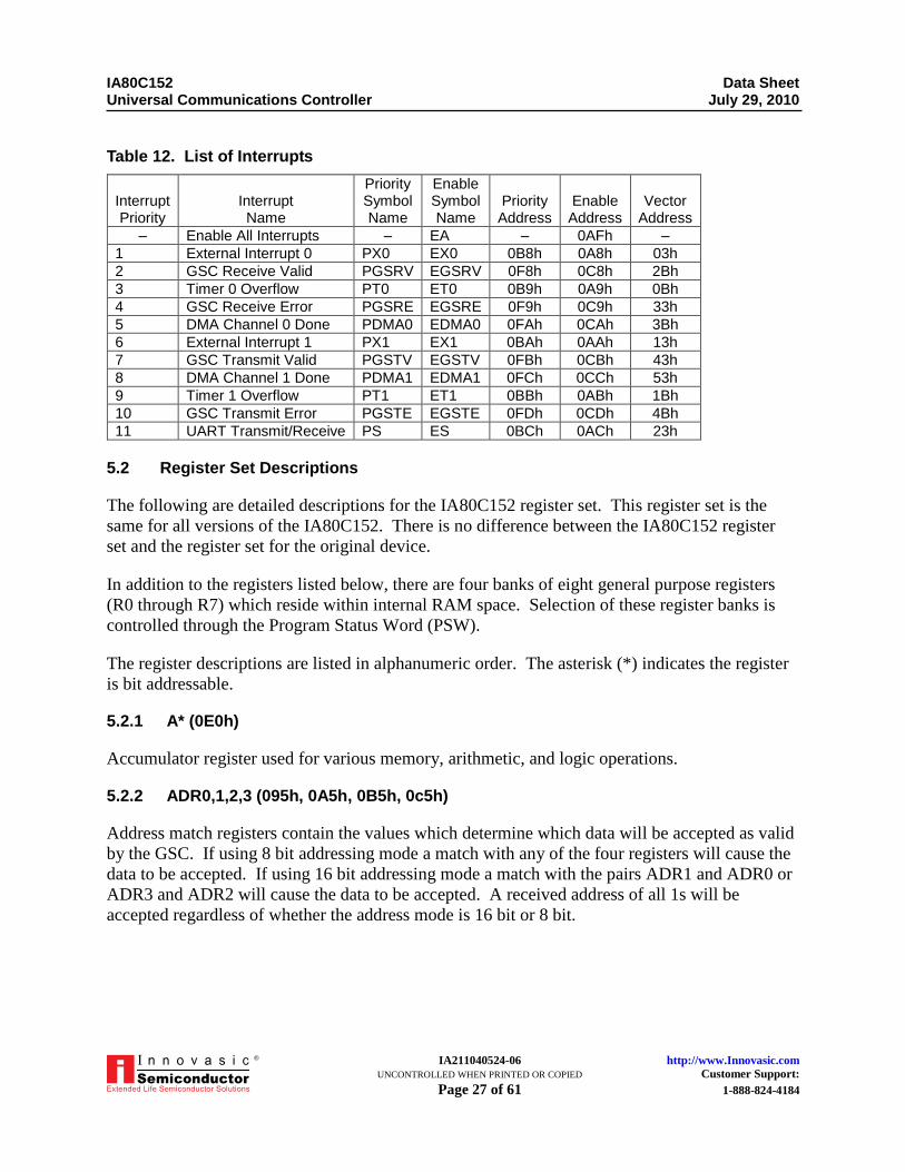
Table 12. List of Interrupts
Interrupt Priority
Interrupt Name
Priority Symbol Name
Enable Symbol Name
Priority Address
Enable Address
Vector Address
– Enable All Interrupts – EA – 0AFh –
1 External Interrupt 0 PX0 EX0 0B8h 0A8h 03h
2 GSC Receive Valid PGSRV EGSRV 0F8h 0C8h 2Bh
3 Timer 0 Overflow PT0 ET0 0B9h 0A9h 0Bh
4 GSC Receive Error PGSRE EGSRE 0F9h 0C9h 33h
5 DMA Channel 0 Done PDMA0 EDMA0 0FAh 0CAh 3Bh
6 External Interrupt 1 PX1 EX1 0BAh 0AAh 13h
7 GSC Transmit Valid PGSTV EGSTV 0FBh 0CBh 43h
8 DMA Channel 1 Done PDMA1 EDMA1 0FCh 0CCh 53h
9 Timer 1 Overflow PT1 ET1 0BBh 0ABh 1Bh
10 GSC Transmit Error PGSTE EGSTE 0FDh 0CDh 4Bh
11 UART Transmit/Receive PS ES 0BCh 0ACh 23h
5.2 Register Set Descriptions
The following are detailed descriptions for the IA80C152 register set. This register set is the
same for all versions of the IA80C152. There is no difference between the IA80C152 register
set and the register set for the original device.
In addition to the registers listed below, there are four banks of eight general purpose registers
(R0 through R7) which reside within internal RAM space. Selection of these register banks is
controlled through the Program Status Word (PSW).
The register descriptions are listed in alphanumeric order. The asterisk (*) indicates the register
is bit addressable.
5.2.1 A* (0E0h)
Accumulator register used for various memory, arithmetic, and logic operations.
5.2.2 ADR0,1,2,3 (095h, 0A5h, 0B5h, 0c5h)
Address match registers contain the values which determine which data will be accepted as valid
by the GSC. If using 8 bit addressing mode a match with any of the four registers will cause the
data to be accepted. If using 16 bit addressing mode a match with the pairs ADR1 and ADR0 or
ADR3 and ADR2 will cause the data to be accepted. A received address of all 1s will be
accepted regardless of whether the address mode is 16 bit or 8 bit.
IA80C152 Data Sheet Universal Communications Controller July 29, 2010
IA211040524-06 http://www.Innovasic.com UNCONTROLLED WHEN PRINTED OR COPIED Customer Support: Page 28 of 61 1-888-824-4184
®
5.2.3 AMSK0,1 (0D5h, 0E5h)
Address Match Mask registers are used to set the corresponding bit in Address match registers to
don’t care. Setting the bit to a one in the AMSK register sets the corresponding bit in the ADR
register to don’t care.
5.2.4 B* (0F0h)
The B register used for multiply and divide instructions. May also be used as a general purpose
register.
5.2.5 BAUD (094h)
Contains the value to be used by the baud rate determining equation. The value written to
BAUD will actually be stored in a reload register. When the BAUD register contents are
decremented to 00H the BAUD register will be reloaded from the reload register. Reading the
BAUD register yields the current baud rate timer value. A read during a GSC operation may not
give the current value because the value in BAUD could decrement after it is read and before the
read value can be stored in its destination. BAUD rate = Fosc/((BAUD + 1)*8)
5.2.6 BCRL0, BCRH0 (0E2h, 0E3h)
Byte count register low and high bytes for DMA channel 0. The two registers provide a 16-bit
value representing the number of DMA transfers via channel 0. Valid count range is from 0
to 65535.
5.2.7 BCRL1, BCRH1 (0F2h, 0F3h)
Byte count register low and high bytes for DMA channel 1. The two registers provide a 16-bit
value representing the number of DMA transfers via channel 1. Valid count range is from 0
to 65535.
5.2.8 BKOFF (0C4h)
An 8 bit count down timer with a clock period equal to one slot time. A user may read the
register, but the register is clocked asynchronously to the CPU so invalid data can result.
Writing to BKOFF will have no effect.
5.2.9 DARL0, DARH0 (0C2h, 0C3h)
Destination address register low and high bytes for DMA channel 0. The two registers provide a
16-bit value representing the address of the destination for a DMA transfer via channel 0. Valid
address range is from 0 to 65535.

IA80C152 Data Sheet Universal Communications Controller July 29, 2010
IA211040524-06 http://www.Innovasic.com UNCONTROLLED WHEN PRINTED OR COPIED Customer Support: Page 29 of 61 1-888-824-4184
®
5.2.10 DARL1, DARH1 (0D2h, 0D3h)
Destination address register low and high bytes for DMA channel 1. The two registers provide a
16-bit value representing the address of the destination for a DMA transfer via channel 1. Valid
address range is from 0 to 65535.
5.2.11 DCON0,1 (092h, 093h)
DCON0 and DCON1 control DMA channel 0 or 1, respectively. Each bit in these 8-bit registers
control the DMA transfer as described in Table 13.
Table 13. DCON0,1 Register
7 6 5 4 3 2 1 0
DAS IDA SAS ISA DM TM DONE GO
Bit [7]—DAS → This bit in conjunction with IDA determines the destination address
space.
Bit [6]—IDA → If IDA is set to 1 then the destination address is automatically
incremented after the transfer of each byte.
DAS IDA Destination Auto-Increment
0 0 External Ram NO
0 1 External Ram YES
1 0 SFR NO
1 1 Internal RAM YES
Bit [5]—SAS → This bit in conjunction with ISA determines the source address space.
Bit [4]—ISA → If ISA is set to 1, the source address is automatically incremented after
the transfer of each byte.
SAS ISA Source Auto-Increment
0 0 External Ram NO
0 1 External Ram YES
1 0 SFR NO
1 1 Internal RAM YES
Bit [3]—DM → If this bit is set to 1, the DMA channel operates in demand mode. In this
mode the DMA is initiated by either an external signal or by a serial port flag depending
on the value of the TM bit. If the DM bit is set to 0, DMA is initiated by setting the GO
bit.
IA80C152 Data Sheet Universal Communications Controller July 29, 2010
IA211040524-06 http://www.Innovasic.com UNCONTROLLED WHEN PRINTED OR COPIED Customer Support: Page 30 of 61 1-888-824-4184
®
Bit [2]—TM → If DM is 1, TM selects if DMA is initiated by an external signal (TM=1)
or by a serial port bit (TM=0). If DM is 0, TM selects whether DMA transfers are in
burst mode (TM=1) or in alternate cycles mode (TM=0).
DM TM Mode
0 0 Alternate Cycles
0 1 Burst
1 0 LSC/GSC Interrupt Demand
1 1 External Interrupt Demand
Bit [1]—DONE → This bit indicates that the DMA operation has completed. It also
causes an interrupt. This bit is set to 1 when BCRn equals 0 and is set to 0 when the
interrupt is vectored. The user can also set and clear this bit.
Bit [0]—GO → If this bit is set to 1, it enables the DMA channel.
5.2.12 DPL, DPH (082h, 083h)
DPTR, or the ―data pointer‖ consists of the two 8-bit registers, DPL and DPH. The DPTR must
be used for accesses to external memory requiring 16-bit addresses.
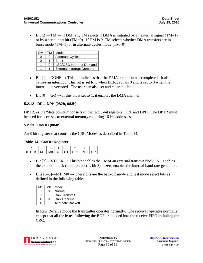
5.2.13 GMOD (084h)
An 8-bit register that controls the GSC Modes as described in Table 14.
Table 14. GMOD Register
7 6 5 4 3 2 1 0
XTCLK M1 M0 AL CT PL1 PL0 PR
Bit [7]—XTCLK → This bit enables the use of an external transmit clock. A 1 enables
the external clock (input on port 1, bit 3), a zero enables the internal baud rate generator.
Bits [6–5]—M1, M0 → These bits are the backoff mode and test mode select bits as
defined in the following table.
M1 M0 Mode
0 0 Normal
0 1 Raw Transmit
1 0 Raw Receive
1 1 Alternate Backoff
In Raw Receive mode the transmitter operates normally. The receiver operates normally
except that all the bytes following the BOF are loaded into the receive FIFO including the
CRC.
IA80C152 Data Sheet Universal Communications Controller July 29, 2010
IA211040524-06 http://www.Innovasic.com UNCONTROLLED WHEN PRINTED OR COPIED Customer Support: Page 31 of 61 1-888-824-4184
®
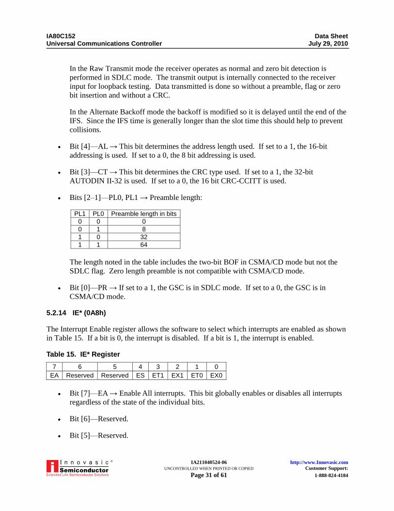
In the Raw Transmit mode the receiver operates as normal and zero bit detection is
performed in SDLC mode. The transmit output is internally connected to the receiver
input for loopback testing. Data transmitted is done so without a preamble, flag or zero
bit insertion and without a CRC.
In the Alternate Backoff mode the backoff is modified so it is delayed until the end of the
IFS. Since the IFS time is generally longer than the slot time this should help to prevent
collisions.
Bit [4]—AL → This bit determines the address length used. If set to a 1, the 16-bit
addressing is used. If set to a 0, the 8 bit addressing is used.
Bit [3]—CT → This bit determines the CRC type used. If set to a 1, the 32-bit
AUTODIN II-32 is used. If set to a 0, the 16 bit CRC-CCITT is used.
Bits [2–1]—PL0, PL1 → Preamble length:
PL1 PL0 Preamble length in bits
0 0 0
0 1 8
1 0 32
1 1 64
The length noted in the table includes the two-bit BOF in CSMA/CD mode but not the
SDLC flag. Zero length preamble is not compatible with CSMA/CD mode.
Bit [0]—PR → If set to a 1, the GSC is in SDLC mode. If set to a 0, the GSC is in
CSMA/CD mode.
5.2.14 IE* (0A8h)
The Interrupt Enable register allows the software to select which interrupts are enabled as shown
in Table 15. If a bit is 0, the interrupt is disabled. If a bit is 1, the interrupt is enabled.
Table 15. IE* Register
7 6 5 4 3 2 1 0
EA Reserved Reserved ES ET1 EX1 ET0 EX0
Bit [7]—EA → Enable All interrupts. This bit globally enables or disables all interrupts
regardless of the state of the individual bits.
Bit [6]—Reserved.
Bit [5]—Reserved.
IA80C152 Data Sheet Universal Communications Controller July 29, 2010
IA211040524-06 http://www.Innovasic.com UNCONTROLLED WHEN PRINTED OR COPIED Customer Support: Page 32 of 61 1-888-824-4184
®
Bit [4]—ES → Enable or disable serial port interrupt.
Bit [3]—ET1 → Enable or disable Timer 1 overflow interrupt.
Bit [2]—EX1 → Enable or disable External Interrupt 1.
Bit [1]—ET0 → Enable or disable Timer 0 overflow interrupt.
Bit [0]—EX0 → Enable or disable External Interrupt 0.
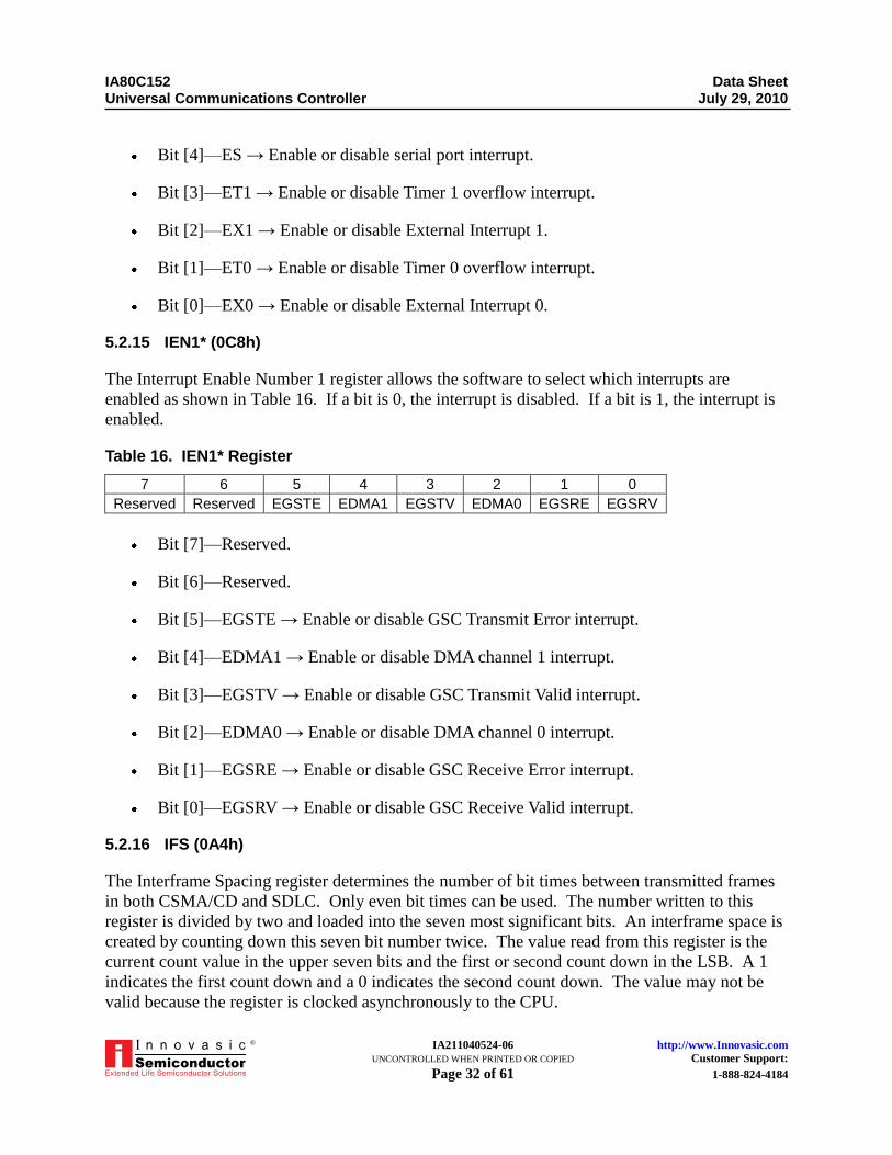
5.2.15 IEN1* (0C8h)
The Interrupt Enable Number 1 register allows the software to select which interrupts are
enabled as shown in Table 16. If a bit is 0, the interrupt is disabled. If a bit is 1, the interrupt is
enabled.
Table 16. IEN1* Register
7 6 5 4 3 2 1 0
Reserved Reserved EGSTE EDMA1 EGSTV EDMA0 EGSRE EGSRV
Bit [7]—Reserved.
Bit [6]—Reserved.
Bit [5]—EGSTE → Enable or disable GSC Transmit Error interrupt.
Bit [4]—EDMA1 → Enable or disable DMA channel 1 interrupt.
Bit [3]—EGSTV → Enable or disable GSC Transmit Valid interrupt.
Bit [2]—EDMA0 → Enable or disable DMA channel 0 interrupt.
Bit [1]—EGSRE → Enable or disable GSC Receive Error interrupt.
Bit [0]—EGSRV → Enable or disable GSC Receive Valid interrupt.
5.2.16 IFS (0A4h)
The Interframe Spacing register determines the number of bit times between transmitted frames
in both CSMA/CD and SDLC. Only even bit times can be used. The number written to this
register is divided by two and loaded into the seven most significant bits. An interframe space is
created by counting down this seven bit number twice. The value read from this register is the
current count value in the upper seven bits and the first or second count down in the LSB. A 1
indicates the first count down and a 0 indicates the second count down. The value may not be
valid because the register is clocked asynchronously to the CPU.
IA80C152 Data Sheet Universal Communications Controller July 29, 2010
IA211040524-06 http://www.Innovasic.com UNCONTROLLED WHEN PRINTED OR COPIED Customer Support: Page 33 of 61 1-888-824-4184
®
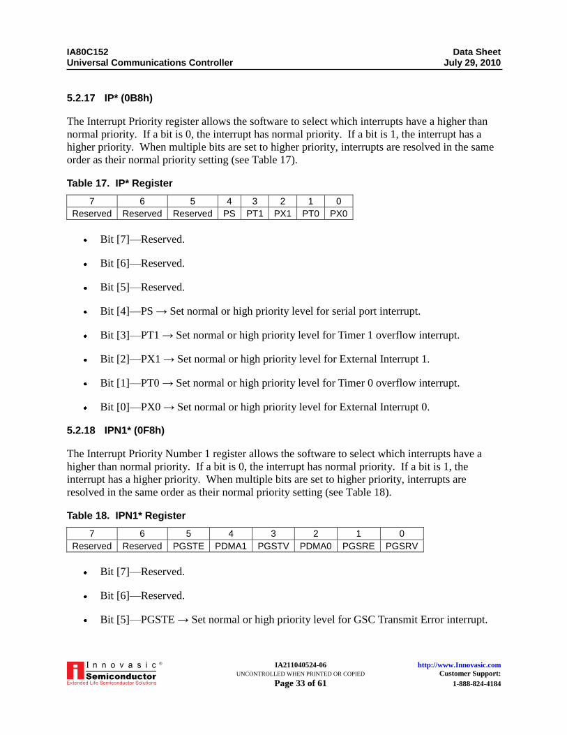
5.2.17 IP* (0B8h)
The Interrupt Priority register allows the software to select which interrupts have a higher than
normal priority. If a bit is 0, the interrupt has normal priority. If a bit is 1, the interrupt has a
higher priority. When multiple bits are set to higher priority, interrupts are resolved in the same
order as their normal priority setting (see Table 17).
Table 17. IP* Register
7 6 5 4 3 2 1 0
Reserved Reserved Reserved PS PT1 PX1 PT0 PX0
Bit [7]—Reserved.
Bit [6]—Reserved.
Bit [5]—Reserved.
Bit [4]—PS → Set normal or high priority level for serial port interrupt.
Bit [3]—PT1 → Set normal or high priority level for Timer 1 overflow interrupt.
Bit [2]—PX1 → Set normal or high priority level for External Interrupt 1.
Bit [1]—PT0 → Set normal or high priority level for Timer 0 overflow interrupt.
Bit [0]—PX0 → Set normal or high priority level for External Interrupt 0.
5.2.18 IPN1* (0F8h)
The Interrupt Priority Number 1 register allows the software to select which interrupts have a
higher than normal priority. If a bit is 0, the interrupt has normal priority. If a bit is 1, the
interrupt has a higher priority. When multiple bits are set to higher priority, interrupts are
resolved in the same order as their normal priority setting (see Table 18).
Table 18. IPN1* Register
7 6 5 4 3 2 1 0
Reserved Reserved PGSTE PDMA1 PGSTV PDMA0 PGSRE PGSRV
Bit [7]—Reserved.
Bit [6]—Reserved.
Bit [5]—PGSTE → Set normal or high priority level for GSC Transmit Error interrupt.
IA80C152 Data Sheet Universal Communications Controller July 29, 2010
IA211040524-06 http://www.Innovasic.com UNCONTROLLED WHEN PRINTED OR COPIED Customer Support: Page 34 of 61 1-888-824-4184
®
Bit [4]—PDMA1 → Set normal or high priority level for DMA channel 1 interrupt.
Bit [3]—PGSTV → Set normal or high priority level for GSC Transmit Valid interrupt.
Bit [2]—PDMA0 → Set normal or high priority level for DMA channel 0 interrupt.
Bit [1]—PGSRE → Set normal or high priority level for GSC Receive Error interrupt.
Bit [0]—PGSRV → Set normal or high priority level for GSC Receive Valid interrupt.
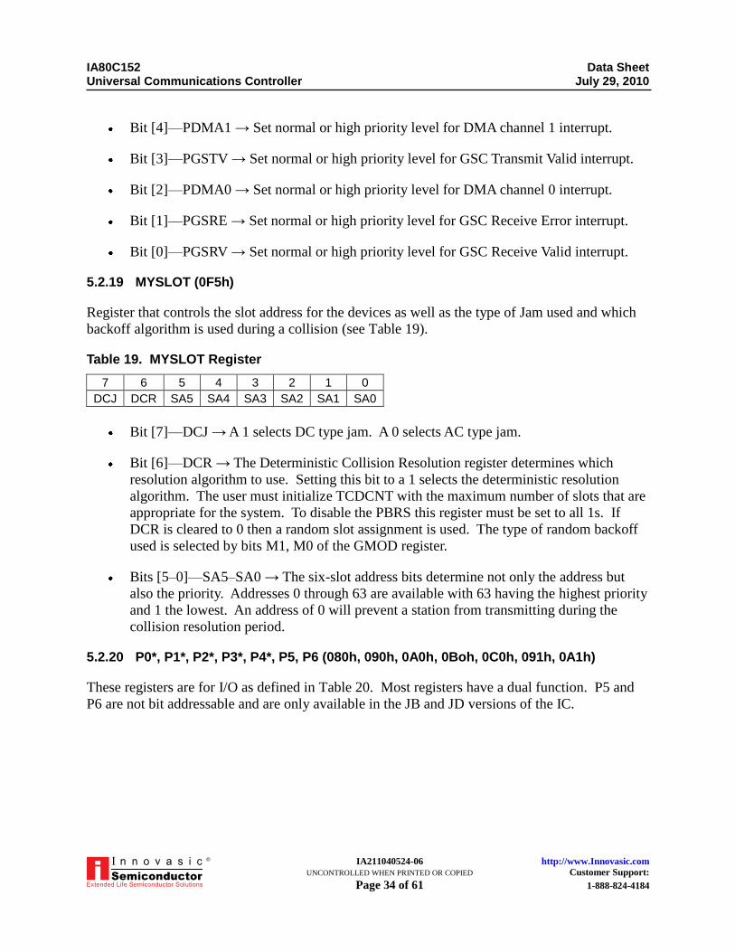
5.2.19 MYSLOT (0F5h)
Register that controls the slot address for the devices as well as the type of Jam used and which
backoff algorithm is used during a collision (see Table 19).
Table 19. MYSLOT Register
7 6 5 4 3 2 1 0
DCJ DCR SA5 SA4 SA3 SA2 SA1 SA0
Bit [7]—DCJ → A 1 selects DC type jam. A 0 selects AC type jam.
Bit [6]—DCR → The Deterministic Collision Resolution register determines which
resolution algorithm to use. Setting this bit to a 1 selects the deterministic resolution
algorithm. The user must initialize TCDCNT with the maximum number of slots that are
appropriate for the system. To disable the PBRS this register must be set to all 1s. If
DCR is cleared to 0 then a random slot assignment is used. The type of random backoff
used is selected by bits M1, M0 of the GMOD register.
Bits [5–0]—SA5–SA0 → The six-slot address bits determine not only the address but
also the priority. Addresses 0 through 63 are available with 63 having the highest priority
and 1 the lowest. An address of 0 will prevent a station from transmitting during the
collision resolution period.
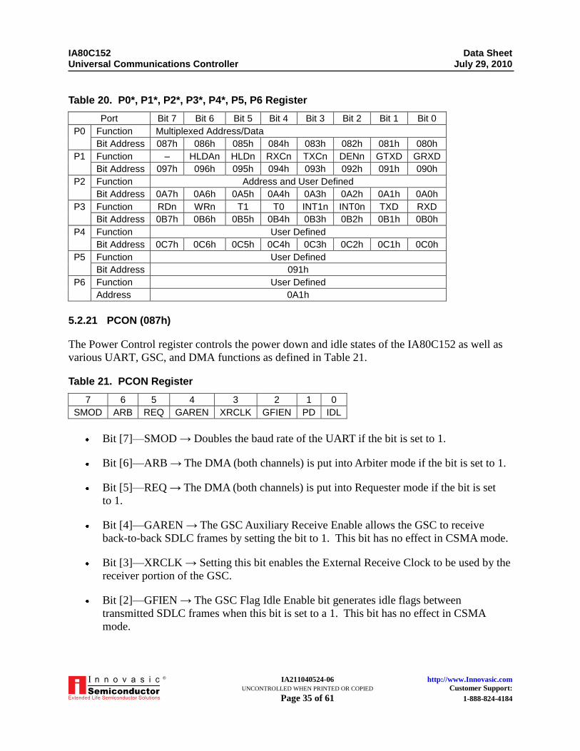
5.2.20 P0*, P1*, P2*, P3*, P4*, P5, P6 (080h, 090h, 0A0h, 0Boh, 0C0h, 091h, 0A1h)
These registers are for I/O as defined in Table 20. Most registers have a dual function. P5 and
P6 are not bit addressable and are only available in the JB and JD versions of the IC.
IA80C152 Data Sheet Universal Communications Controller July 29, 2010
IA211040524-06 http://www.Innovasic.com UNCONTROLLED WHEN PRINTED OR COPIED Customer Support: Page 35 of 61 1-888-824-4184
®
Table 20. P0*, P1*, P2*, P3*, P4*, P5, P6 Register
Port Bit 7 Bit 6 Bit 5 Bit 4 Bit 3 Bit 2 Bit 1 Bit 0
P0 Function Multiplexed Address/Data
Bit Address 087h 086h 085h 084h 083h 082h 081h 080h
P1 Function – HLDAn HLDn RXCn TXCn DENn GTXD GRXD
Bit Address 097h 096h 095h 094h 093h 092h 091h 090h
P2 Function Address and User Defined
Bit Address 0A7h 0A6h 0A5h 0A4h 0A3h 0A2h 0A1h 0A0h
P3 Function RDn WRn T1 T0 INT1n INT0n TXD RXD
Bit Address 0B7h 0B6h 0B5h 0B4h 0B3h 0B2h 0B1h 0B0h
P4 Function User Defined
Bit Address 0C7h 0C6h 0C5h 0C4h 0C3h 0C2h 0C1h 0C0h
P5 Function User Defined
Bit Address 091h
P6 Function User Defined
Address 0A1h
5.2.21 PCON (087h)
The Power Control register controls the power down and idle states of the IA80C152 as well as
various UART, GSC, and DMA functions as defined in Table 21.
Table 21. PCON Register
7 6 5 4 3 2 1 0
SMOD ARB REQ GAREN XRCLK GFIEN PD IDL
Bit [7]—SMOD → Doubles the baud rate of the UART if the bit is set to 1.
Bit [6]—ARB → The DMA (both channels) is put into Arbiter mode if the bit is set to 1.
Bit [5]—REQ → The DMA (both channels) is put into Requester mode if the bit is set
to 1.
Bit [4]—GAREN → The GSC Auxiliary Receive Enable allows the GSC to receive
back-to-back SDLC frames by setting the bit to 1. This bit has no effect in CSMA mode.
Bit [3]—XRCLK → Setting this bit enables the External Receive Clock to be used by the
receiver portion of the GSC.
Bit [2]—GFIEN → The GSC Flag Idle Enable bit generates idle flags between
transmitted SDLC frames when this bit is set to a 1. This bit has no effect in CSMA
mode.
IA80C152 Data Sheet Universal Communications Controller July 29, 2010
IA211040524-06 http://www.Innovasic.com UNCONTROLLED WHEN PRINTED OR COPIED Customer Support: Page 36 of 61 1-888-824-4184
®
Bit [1]—PD → The Power Down bit puts the IA80C152 into the power down power
saving mode by setting this bit to a 1.
Bit [0]—IDL → The Idle bit puts the IA80C152 into the idle power saving mode by
setting this bit to a 1.
5.2.22 PRBS (0E4h)
This register contains the pseudo-random number to be used in the CSMA/CD backoff
algorithm. The number is generated by using a feedback shift register clocked by the CPU phase
clocks. Writing all 1s to this register will cause the register to freeze at all 1s. Writing any other
value to it will cause it to start again. A read of this register will not always give the seed value
due to the register being clocked by the CPUs phase clocks.
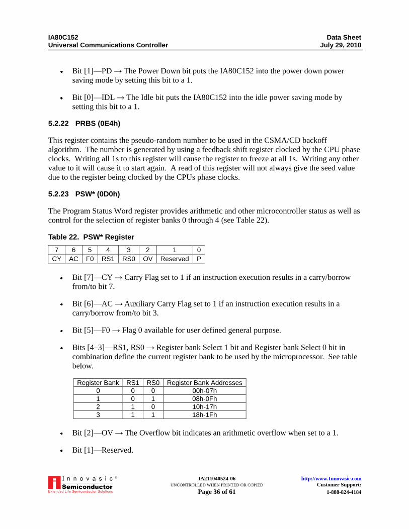
5.2.23 PSW* (0D0h)
The Program Status Word register provides arithmetic and other microcontroller status as well as
control for the selection of register banks 0 through 4 (see Table 22).
Table 22. PSW* Register
7 6 5 4 3 2 1 0
CY AC F0 RS1 RS0 OV Reserved P
Bit [7]—CY → Carry Flag set to 1 if an instruction execution results in a carry/borrow
from/to bit 7.
Bit [6]—AC → Auxiliary Carry Flag set to 1 if an instruction execution results in a
carry/borrow from/to bit 3.
Bit [5]—F0 → Flag 0 available for user defined general purpose.
Bits [4–3]—RS1, RS0 → Register bank Select 1 bit and Register bank Select 0 bit in
combination define the current register bank to be used by the microprocessor. See table
below.
Register Bank RS1 RS0 Register Bank Addresses
0 0 0 00h-07h
1 0 1 08h-0Fh
2 1 0 10h-17h
3 1 1 18h-1Fh
Bit [2]—OV → The Overflow bit indicates an arithmetic overflow when set to a 1.
Bit [1]—Reserved.
IA80C152 Data Sheet Universal Communications Controller July 29, 2010
IA211040524-06 http://www.Innovasic.com UNCONTROLLED WHEN PRINTED OR COPIED Customer Support: Page 37 of 61 1-888-824-4184
®
Bit [0]—P → Parity flag set or cleared by the hardware each instruction to indicate odd
or even number of 1s in the accumulator.
5.2.24 RFIFO (0F4h)
This is a three-byte buffer which points to the oldest data in the buffer. The buffer is loaded with
receive data every time the GSC receiver receives a new byte of data.
5.2.25 RSTAT* (0E8h)
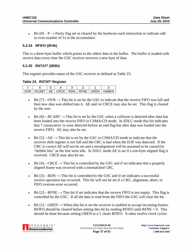
This register provides status of the GSC receiver as defined in Table 23.
Table 23. RSTAT* Register
7 6 5 4 3 2 1 0
OVR RCABT AE CRCE RDN RFNE GREN HABEN
Bit [7]—OVR → This bit is set by the GSC to indicate that the receive FIFO was full and
then new data was shifted into it. AE and /or CRCE may also be set. This flag is cleared
by the user.
Bit [6]—RCABT → This bit is set by the GSC when a collision is detected after data has
been loaded into the receive FIFO in CSMA/CD mode. In SDLC mode this bit indicates
that 7 consecutive 1s were detected before an end flag but after data was loaded into the
receive FIFO. AE may also be set.
Bit [5]—AE → This bit is set by the GSC in CSMA/CD mode to indicate that the
receiver shift register is not full and the CRC is bad when the EOF was detected. If the
CRC is correct AE will not be set and a misalignment will be assumed to be caused by
―dribble bits‖ as the line went idle. In SDLC mode AE is set if a non-byte aligned flag is
received. CRCE may also be set.
Bit [4]—CRCE → This bit is controlled by the GSC and if set indicates that a properly
aligned frame was received with a mismatched CRC.
Bit [3]—RDN → This bit is controlled by the GSC and if set indicates a successful
receive operation has occurred. This bit will not be set if a CRC, alignment, abort, or
FIFO overrun error occurred.
Bit [2]—RFNE → This bit if set indicates that the receive FIFO is not empty. This flag is
controlled by the GSC. If all the data is read from the FIFO the GSC will clear the bit.
Bit [1]—GREN → When this bit is set the receiver is enabled to accept incoming frames.
RFIFO should be cleared before setting this bit by reading RFIFO until RFNE = 0. This
should be done because setting GREN to a 1 clears RFIFO. It takes twelve clock cycles
IA80C152 Data Sheet Universal Communications Controller July 29, 2010
IA211040524-06 http://www.Innovasic.com UNCONTROLLED WHEN PRINTED OR COPIED Customer Support: Page 38 of 61 1-888-824-4184
®
for the status of RFNE to be updated after a read of RFIFO. Setting GREN also clears
RDN, CRCE, AE and RCABT. GREN is cleared by hardware at the end of a reception
or if receive errors are encountered. The user is responsible for setting this bit to a 1.
The user or the GSC can set this bit to a 0. In CSMA/CD mode the status of GREN has
no effect on whether the receiver detects a collision because the receiver always
monitors the receive pin.
Bit [0]—HABEN → The Hardware Based Acknowledge Enable when set to a 1 enables
this feature.
5.2.26 SARL0, SARH0 (0A2h, 0A3h)
Source address register low and high bytes for DMA channel 0. The two registers provide a
16-bit value representing the address of the source for a DMA transfer via channel 0. Valid
address range is from 0 to 65535.
5.2.27 SARL1, SARH1 (0B2h, 0B3h)
Source address register low and high bytes for DMA channel 1. The two registers provide a
16-bit value representing the address of the source for a DMA transfer via channel 1. Valid
address range is from 0 to 65535.
5.2.28 SBUF (099h)
Writes to this register load the transmit register, and reads access the receive register of the LSC.
5.2.29 SCON* (098h)
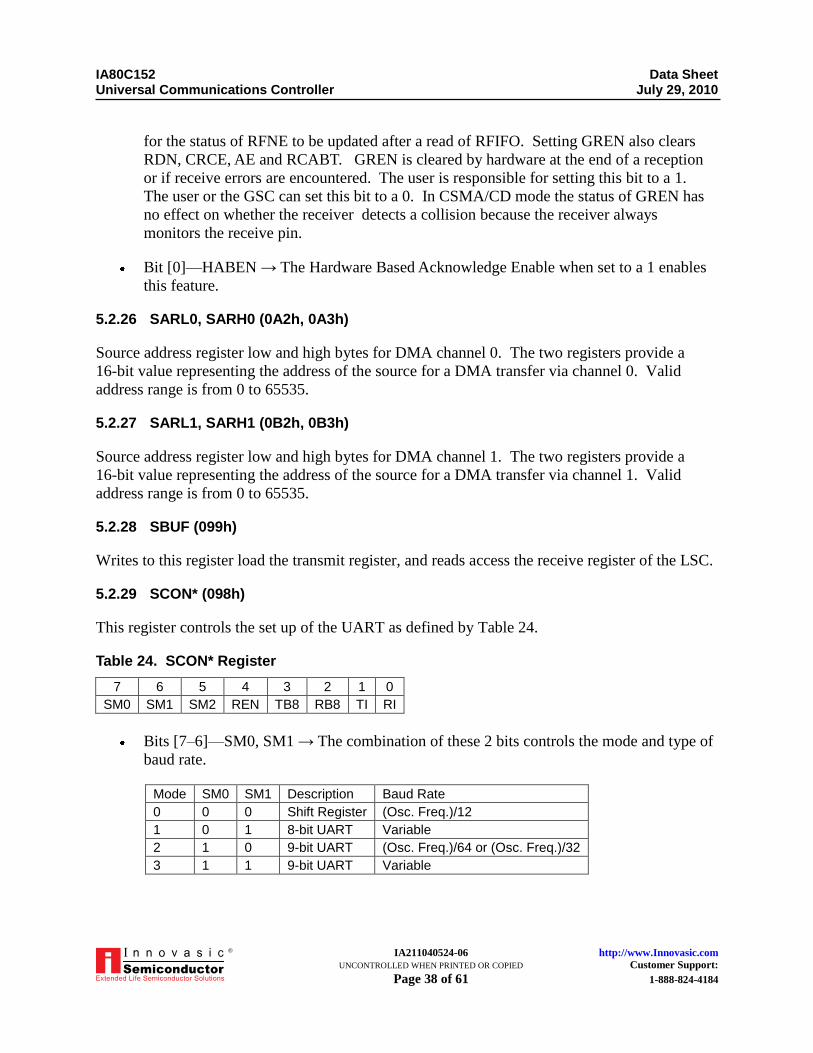
This register controls the set up of the UART as defined by Table 24.
Table 24. SCON* Register
7 6 5 4 3 2 1 0
SM0 SM1 SM2 REN TB8 RB8 TI RI
Bits [7–6]—SM0, SM1 → The combination of these 2 bits controls the mode and type of
baud rate.
Mode SM0 SM1 Description Baud Rate
0 0 0 Shift Register (Osc. Freq.)/12
1 0 1 8-bit UART Variable
2 1 0 9-bit UART (Osc. Freq.)/64 or (Osc. Freq.)/32
3 1 1 9-bit UART Variable
IA80C152 Data Sheet Universal Communications Controller July 29, 2010
IA211040524-06 http://www.Innovasic.com UNCONTROLLED WHEN PRINTED OR COPIED Customer Support: Page 39 of 61 1-888-824-4184
®
Bit [5]—SM2 → When this bit is set and the UART mode is 1, RI will not be activated
unless a valid stop bit is received. When this bit is set and the UART mode is 2 or 3, RI
will not be activated if the 9th bit is 0. In mode 0 SM2 should be set to 0.
Bit [4]—REN → Setting this bit enables the UART to receive. Clearing this bit disables
UART reception.
Bit [3]—TB8 → In modes 2 and 3, the value of this bit is transmitted during the 9th bit
time. This bit is set or cleared by software.
Bit [2]—RB8 → In modes 2 and 3, this bit is the value of the 9th bit that was received by
the UART. In mode 1 with SM2 = 1, this bit is the value of the stop bit received by the
UART. In mode 0 RB8 is not used.
Bit [2]—TI → Transmit Interrupt flag set by hardware at the end of the 8th bit in mode 0
or at the beginning of the stop bit in modes 1, 2, or 3. This bit must be cleared by
software to clear the interrupt.
Bit [0]—RI → Receive Interrupt flag set by hardware at the end of the 8th bit in mode 0
or halfway through the stop bit in modes 1, 2, or 3. This bit must be cleared by software
to clear the interrupt.
5.2.30 SLOTTM (0B4h)
Determines the length of the slot time in CSMA/CD mode. A slot time equals SLOTTM *
(1/baud rate). Reads from this location are unreliable because this register is clocked
asynchronously to the CPU. Loading a value of 0 results in a slot time of 256 bit times.
5.2.31 SP (081h)
This register is the stack pointer. Its value points to the memory location that is the beginning of
the stack.
5.2.32 TCDCNT (0D4h)
If probabilistic CSMA/CD is used this register contains the number of collisions. The user must
clear this register before transmitting a new frame so the GSC can distinguish between a new
frame and the retransmit of a frame. In deterministic backoff mode TCDCNT is used to hold the
maximum number of slots.
5.2.33 TCON* (088h)
This register controls the operation of the Timers 0 and 1 and External Interrupts 0 and 1 as
defined by Table 25.
IA80C152 Data Sheet Universal Communications Controller July 29, 2010
IA211040524-06 http://www.Innovasic.com UNCONTROLLED WHEN PRINTED OR COPIED Customer Support: Page 40 of 61 1-888-824-4184
®
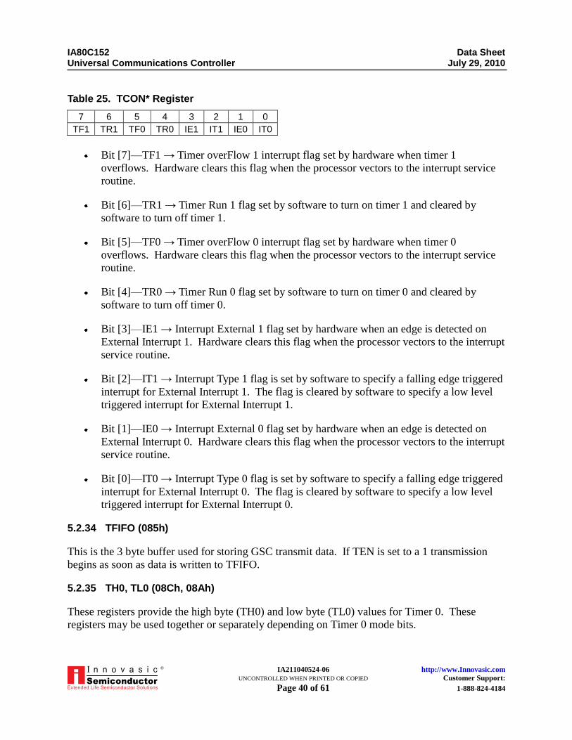
Table 25. TCON* Register
7 6 5 4 3 2 1 0
TF1 TR1 TF0 TR0 IE1 IT1 IE0 IT0
Bit [7]—TF1 → Timer overFlow 1 interrupt flag set by hardware when timer 1
overflows. Hardware clears this flag when the processor vectors to the interrupt service
routine.
Bit [6]—TR1 → Timer Run 1 flag set by software to turn on timer 1 and cleared by
software to turn off timer 1.
Bit [5]—TF0 → Timer overFlow 0 interrupt flag set by hardware when timer 0
overflows. Hardware clears this flag when the processor vectors to the interrupt service
routine.
Bit [4]—TR0 → Timer Run 0 flag set by software to turn on timer 0 and cleared by
software to turn off timer 0.
Bit [3]—IE1 → Interrupt External 1 flag set by hardware when an edge is detected on
External Interrupt 1. Hardware clears this flag when the processor vectors to the interrupt
service routine.
Bit [2]—IT1 → Interrupt Type 1 flag is set by software to specify a falling edge triggered
interrupt for External Interrupt 1. The flag is cleared by software to specify a low level
triggered interrupt for External Interrupt 1.
Bit [1]—IE0 → Interrupt External 0 flag set by hardware when an edge is detected on
External Interrupt 0. Hardware clears this flag when the processor vectors to the interrupt
service routine.
Bit [0]—IT0 → Interrupt Type 0 flag is set by software to specify a falling edge triggered
interrupt for External Interrupt 0. The flag is cleared by software to specify a low level
triggered interrupt for External Interrupt 0.
5.2.34 TFIFO (085h)
This is the 3 byte buffer used for storing GSC transmit data. If TEN is set to a 1 transmission
begins as soon as data is written to TFIFO.
5.2.35 TH0, TL0 (08Ch, 08Ah)
These registers provide the high byte (TH0) and low byte (TL0) values for Timer 0. These
registers may be used together or separately depending on Timer 0 mode bits.
IA80C152 Data Sheet Universal Communications Controller July 29, 2010
IA211040524-06 http://www.Innovasic.com UNCONTROLLED WHEN PRINTED OR COPIED Customer Support: Page 41 of 61 1-888-824-4184
®
5.2.36 TH1, TL1 (08Dh, 08Bh)
These registers provide the high byte (TH0) and low byte (TL0) values for Timer 0. These
registers may be used together or separately depending on Timer 0 mode bits.
5.2.37 TMOD (089h)
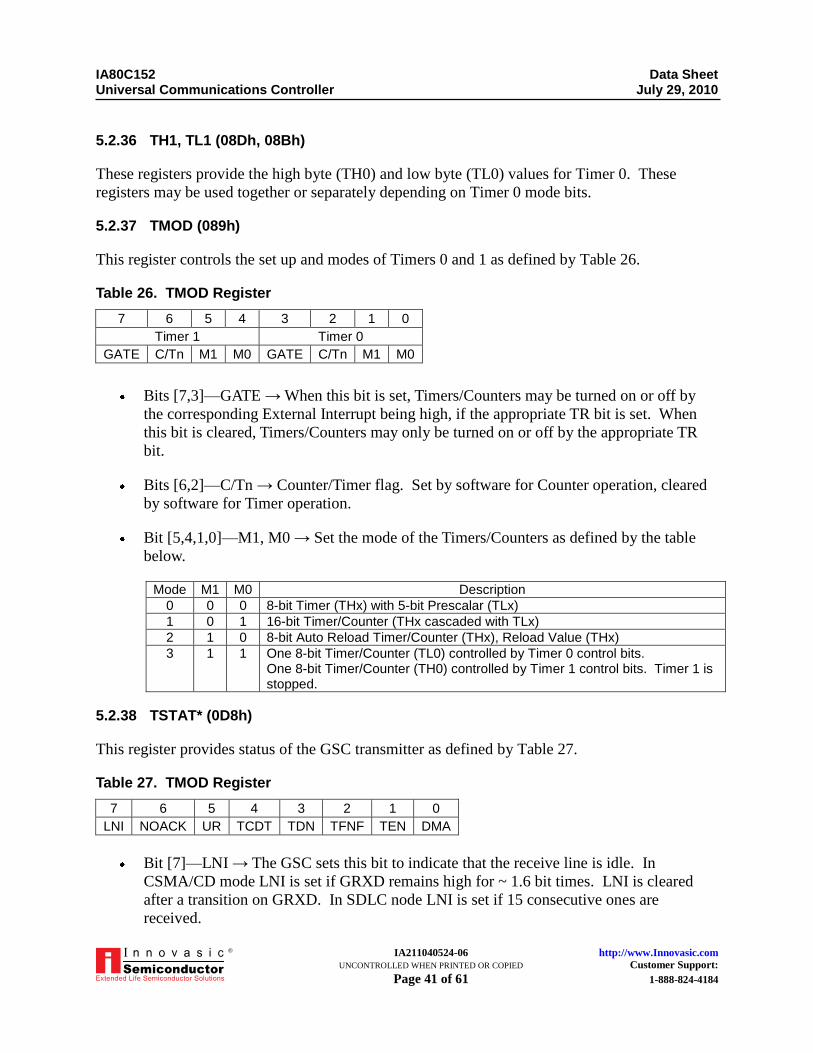
This register controls the set up and modes of Timers 0 and 1 as defined by Table 26.
Table 26. TMOD Register
7 6 5 4 3 2 1 0
Timer 1 Timer 0
GATE C/Tn M1 M0 GATE C/Tn M1 M0
Bits [7,3]—GATE → When this bit is set, Timers/Counters may be turned on or off by
the corresponding External Interrupt being high, if the appropriate TR bit is set. When
this bit is cleared, Timers/Counters may only be turned on or off by the appropriate TR
bit.
Bits [6,2]—C/Tn → Counter/Timer flag. Set by software for Counter operation, cleared
by software for Timer operation.
Bit [5,4,1,0]—M1, M0 → Set the mode of the Timers/Counters as defined by the table
below.
Mode M1 M0 Description
0 0 0 8-bit Timer (THx) with 5-bit Prescalar (TLx)
1 0 1 16-bit Timer/Counter (THx cascaded with TLx)
2 1 0 8-bit Auto Reload Timer/Counter (THx), Reload Value (THx)
3 1 1 One 8-bit Timer/Counter (TL0) controlled by Timer 0 control bits. One 8-bit Timer/Counter (TH0) controlled by Timer 1 control bits. Timer 1 is stopped.
5.2.38 TSTAT* (0D8h)
This register provides status of the GSC transmitter as defined by Table 27.
Table 27. TMOD Register
7 6 5 4 3 2 1 0
LNI NOACK UR TCDT TDN TFNF TEN DMA
Bit [7]—LNI → The GSC sets this bit to indicate that the receive line is idle. In
CSMA/CD mode LNI is set if GRXD remains high for ~ 1.6 bit times. LNI is cleared
after a transition on GRXD. In SDLC node LNI is set if 15 consecutive ones are
received.
IA80C152 Data Sheet Universal Communications Controller July 29, 2010
IA211040524-06 http://www.Innovasic.com UNCONTROLLED WHEN PRINTED OR COPIED Customer Support: Page 42 of 61 1-888-824-4184
®
Bit [6]—NOACK → The GSC sets this bit to indicate that an acknowledge was not
received for the previous frame. This bit will be set only if HABEN is set and no
acknowledge is received before the end of the IFS. NOACK will not be set following a
broadcast or a multi-cast packet.
Bit [5]—UR → The GSC sets this bit to indicate that in DMA mode the last bit was
shifted out of the transmit register and that the DMA byte count did not equal 0. When
this occurs the transmitter stops without sending the CRC and the end flag.
Bit [4]—TCDT → The GSC sets this bit to indicate that the transmission stopped due to a
collision. The bit is set by a collision occurring during the data, the CRC or if there are
more than 8 collisions.
Bit [3]—TDN → The GSC sets this bit to indicate that a frame transmission completed
successfully. If HABEN is set, TDN will not be set until the end of the IFS so that the
acknowledge can be checked. TDN will not be set if an acknowledge is expected but not
received. An acknowledge will not be expected after a broadcast or a multi-cast packet.
Bit [2]—TFNF → If this bit is a 1 TFIFO is not full and new data may be written to it.
Bit [1]—TEN → When TEN is set it will cause TDN, UR, TCDT and NOACK to be
reset and the TFIFO to be cleared. The transmitter will clear TEN after a successful
transmission, a collision during data, CRC or end flag. The user sets the bit and the user
of the GSC can clear the bit. If the bit is cleared during a transmission the transmit pin
goes to a high level. This is the method used to send an abort character in SDLC. DEN
is also forced to a high level. An end of transmission occurs whenever the TFIFO is
emptied.
Bit [0]—DMA → If this bit is set it indicates that the DMA channels are used to service
the RFIFO and TFIFO and that GSC interrupts occur on TDN and RDN. If set it also
enables UR to become set. If this bit is cleared it indicates that the GSC is operating in
normal mode and interrupts occur on TFNF and RFNE.
5.3 Power Conservation Modes
There are 2 power conservation modes identified as Idle Mode and Power Down Mode. The
IA80C152 pins will have values according to the Table 28 below.
Idle Mode is entered through software control of the PCON register. Idle halts processor
execution and the DMA. The GSC continues to operate to the extent that it can without the
processor or DMA servicing its requests. Idle mode is exited upon receipt of any enabled
interrupt or invoking a hardware reset.
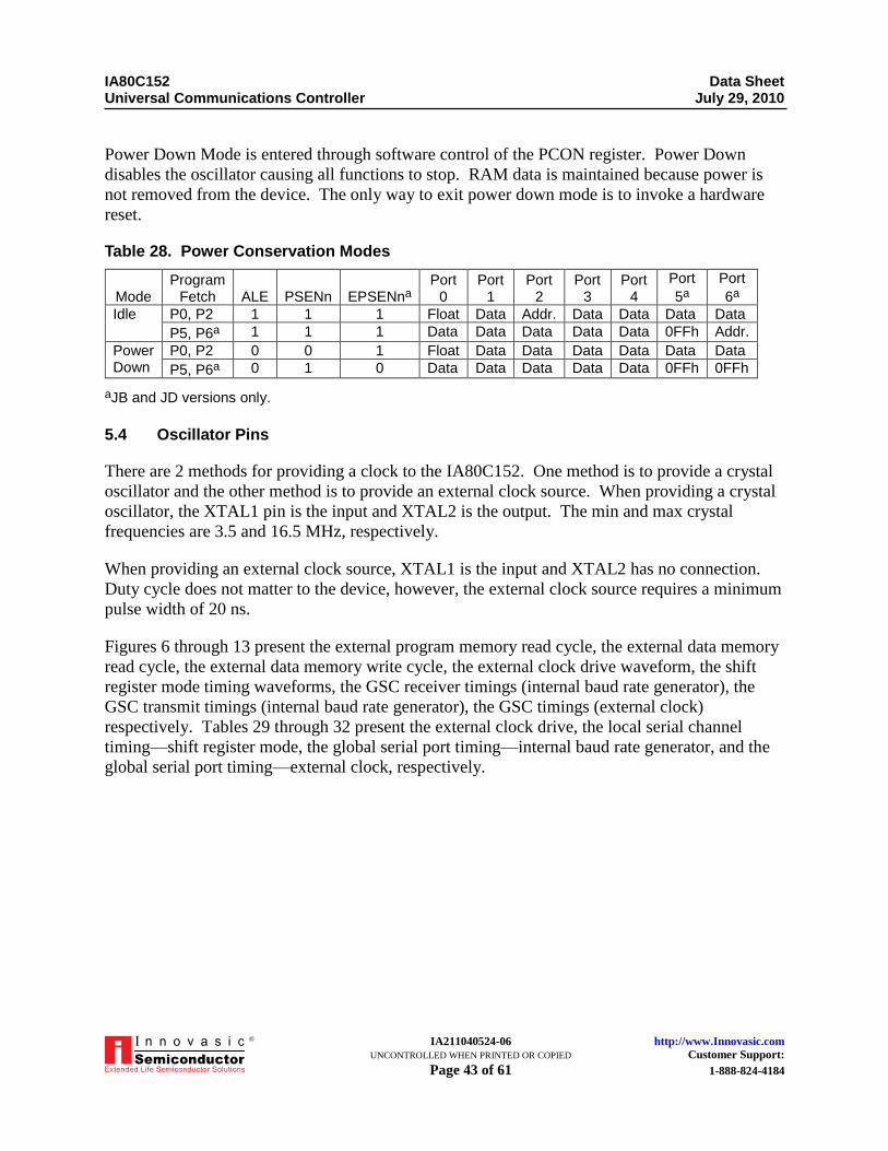
IA80C152 Data Sheet Universal Communications Controller July 29, 2010
IA211040524-06 http://www.Innovasic.com UNCONTROLLED WHEN PRINTED OR COPIED Customer Support: Page 43 of 61 1-888-824-4184
®
Power Down Mode is entered through software control of the PCON register. Power Down
disables the oscillator causing all functions to stop. RAM data is maintained because power is
not removed from the device. The only way to exit power down mode is to invoke a hardware
reset.
Table 28. Power Conservation Modes
Mode Program
Fetch ALE PSENn EPSENna Port
0 Port
1 Port
2 Port
3 Port
4
Port
5a
Port
6a
Idle P0, P2 1 1 1 Float Data Addr. Data Data Data Data
P5, P6a 1 1 1 Data Data Data Data Data 0FFh Addr.
Power Down
P0, P2 0 0 1 Float Data Data Data Data Data Data
P5, P6a 0 1 0 Data Data Data Data Data 0FFh 0FFh
aJB and JD versions only.
5.4 Oscillator Pins
There are 2 methods for providing a clock to the IA80C152. One method is to provide a crystal
oscillator and the other method is to provide an external clock source. When providing a crystal
oscillator, the XTAL1 pin is the input and XTAL2 is the output. The min and max crystal
frequencies are 3.5 and 16.5 MHz, respectively.
When providing an external clock source, XTAL1 is the input and XTAL2 has no connection.
Duty cycle does not matter to the device, however, the external clock source requires a minimum
pulse width of 20 ns.
Figures 6 through 13 present the external program memory read cycle, the external data memory
read cycle, the external data memory write cycle, the external clock drive waveform, the shift
register mode timing waveforms, the GSC receiver timings (internal baud rate generator), the
GSC transmit timings (internal baud rate generator), the GSC timings (external clock)
respectively. Tables 29 through 32 present the external clock drive, the local serial channel
timing—shift register mode, the global serial port timing—internal baud rate generator, and the
global serial port timing—external clock, respectively.
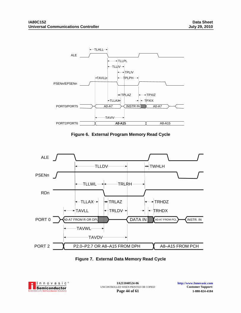
IA80C152 Data Sheet Universal Communications Controller July 29, 2010
IA211040524-06 http://www.Innovasic.com UNCONTROLLED WHEN PRINTED OR COPIED Customer Support: Page 44 of 61 1-888-824-4184
®
ALE
PSENn/EPSENn
PORT0/PORT5
PORT2/PORT6
A0-A7 INSTR IN A0-A7
A8-A15 A8-A15 A8-A15
TLHLL
TLLPL
TPLPH TAVLL
TLLIV
TPLIV
TPLAZ
TLLAX TPXIX
TPXIZ
TAVIV
Figure 6. External Program Memory Read Cycle
Figure 7. External Data Memory Read Cycle
ALE
PSENn
RDn
PORT 0
PORT 2
A0-A7 FROM R OR DPL DATA IN A0-A7 FROM PCL INSTR. IN
P2.0–P2.7 OR A8–A15 FROM DPH A8–A15 FROM PCH
TWHLH TLLDV
TLLWL TRLRH
TAVLL
TLLAX
TRLDV
TRLAZ
TRHDX
TRHDZ
TAVDV
TAVWL
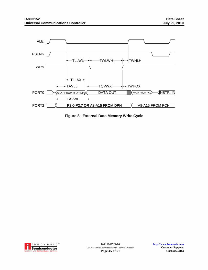
IA80C152 Data Sheet Universal Communications Controller July 29, 2010
IA211040524-06 http://www.Innovasic.com UNCONTROLLED WHEN PRINTED OR COPIED Customer Support: Page 45 of 61 1-888-824-4184
®
ALE
PSENn
WRn
PORT0
PORT2
A0-A7 FROM R OR DPL DATA OUT A0-A7 FROM PCL INSTR. IN
P2.0-P2.7 OR A8-A15 FROM DPH A8-A15 FROM PCH P2.0-P2.7 OR A8-A15 FROM DPH
TWHLH TLLWL TWLWH
TQVWX TAVLL
TLLAX
TWHQX
TAVWL
Figure 8. External Data Memory Write Cycle
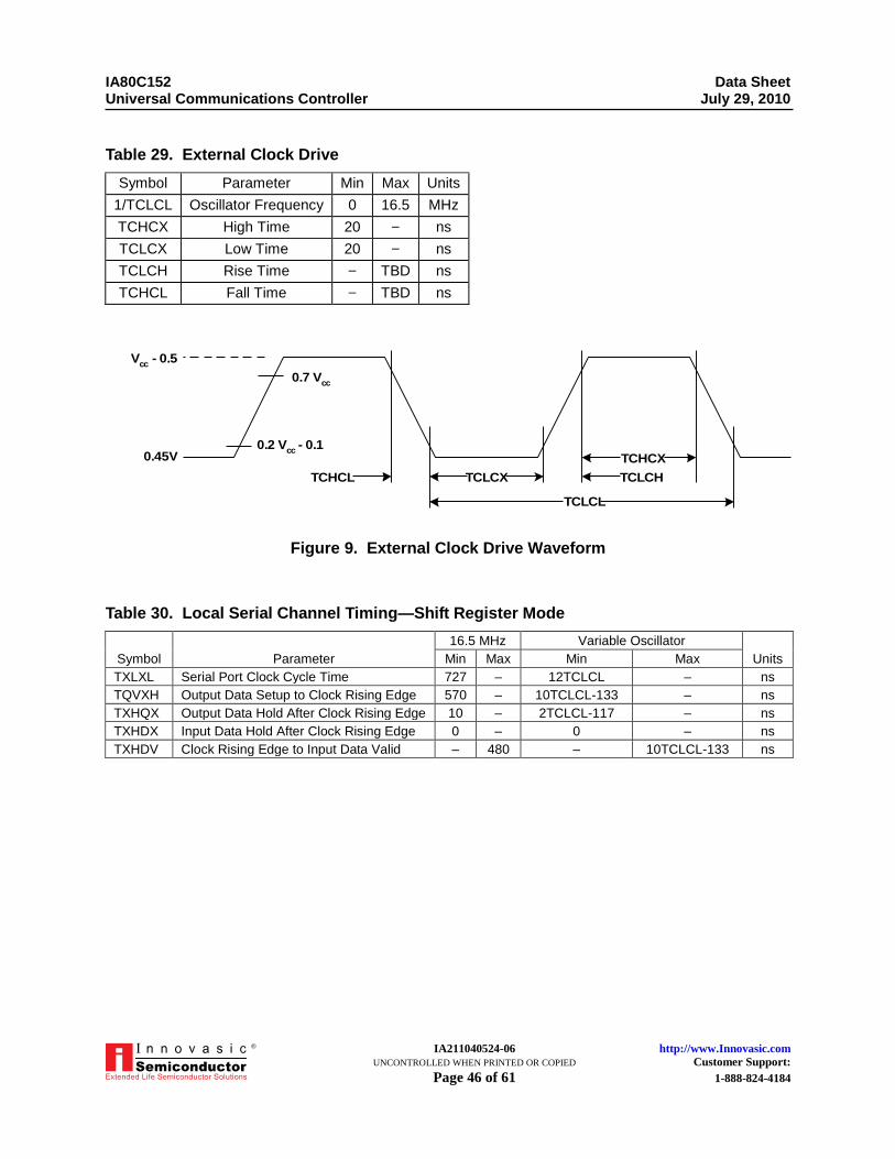
IA80C152 Data Sheet Universal Communications Controller July 29, 2010
IA211040524-06 http://www.Innovasic.com UNCONTROLLED WHEN PRINTED OR COPIED Customer Support: Page 46 of 61 1-888-824-4184
®
Table 29. External Clock Drive
Symbol Parameter Min Max Units
1/TCLCL Oscillator Frequency 0 16.5 MHz
TCHCX High Time 20 – ns
TCLCX Low Time 20 – ns
TCLCH Rise Time – TBD ns
TCHCL Fall Time – TBD ns
Vcc
- 0.5
0.7 Vcc
0.2 Vcc
- 0.10.45V
TCHCL TCLCX
TCHCX
TCLCH
TCLCL
Figure 9. External Clock Drive Waveform
Table 30. Local Serial Channel Timing—Shift Register Mode
Symbol Parameter
16.5 MHz Variable Oscillator
Units Min Max Min Max
TXLXL Serial Port Clock Cycle Time 727 – 12TCLCL – ns
TQVXH Output Data Setup to Clock Rising Edge 570 – 10TCLCL-133 – ns
TXHQX Output Data Hold After Clock Rising Edge 10 – 2TCLCL-117 – ns
TXHDX Input Data Hold After Clock Rising Edge 0 – 0 – ns
TXHDV Clock Rising Edge to Input Data Valid – 480 – 10TCLCL-133 ns
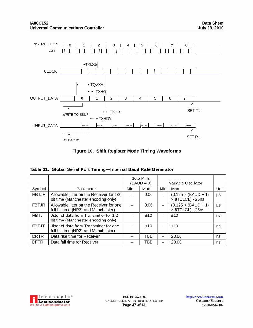
IA80C152 Data Sheet Universal Communications Controller July 29, 2010
IA211040524-06 http://www.Innovasic.com UNCONTROLLED WHEN PRINTED OR COPIED Customer Support: Page 47 of 61 1-888-824-4184
®
VALID VALID VALID VALID
TXLXL
TXHQX
TQVXH
TXHDX
TXHDV
| 0 | | | | | | | | | 1 2 3 4 5 6 7 8
|____________|
|_________| ^ |
WRITE TO SBUF
CLEAR R1 ^ |
^ |
^ |
SET T1
SET R1
INSTRUCTION
ALE
CLOCK
OUTPUT_DATA
INPUT_DATA
0 1 2 3 4 5 6 7 7
VALID VALID VALID VALID VALID
Figure 10. Shift Register Mode Timing Waveforms
Table 31. Global Serial Port Timing—Internal Baud Rate Generator
Symbol Parameter
16.5 MHz (BAUD = 0) Variable Oscillator
Unit Min Max Min Max
HBTJR Allowable jitter on the Receiver for 1/2 bit time (Manchester encoding only)
– 0.06 – (0.125 × (BAUD + 1) × 8TCLCL) - 25ns
µs
FBTJR Allowable jitter on the Receiver for one full bit time (NRZI and Manchester)
– 0.06 – (0.125 × (BAUD + 1) × 8TCLCL) - 25ns
µs
HBTJT Jitter of data from Transmitter for 1/2 bit time (Manchester encoding only)
– ±10 – ±10 ns
FBTJT Jitter of data from Transmitter for one full bit time (NRZI and Manchester)
– ±10 – ±10 ns
DRTR Data rise time for Receiver – TBD – 20.00 ns
DFTR Data fall time for Receiver – TBD – 20.00 ns
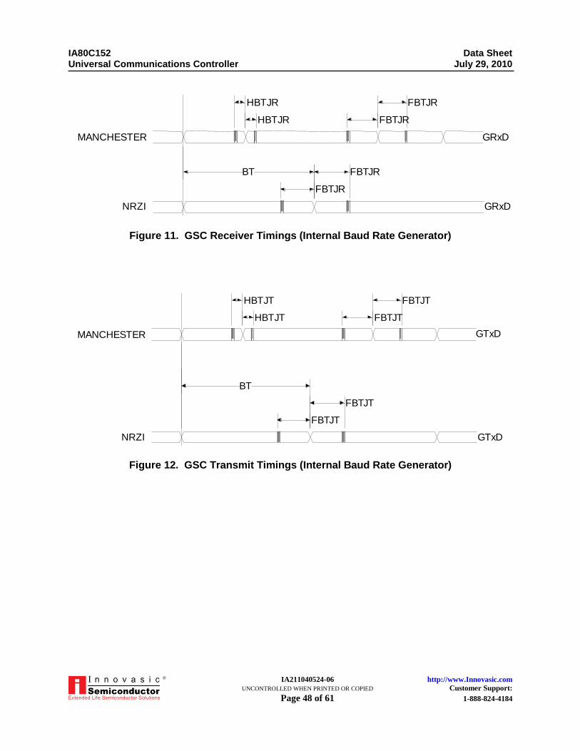
IA80C152 Data Sheet Universal Communications Controller July 29, 2010
IA211040524-06 http://www.Innovasic.com UNCONTROLLED WHEN PRINTED OR COPIED Customer Support: Page 48 of 61 1-888-824-4184
®
MANCHESTER
NRZI
BT
HBTJR
HBTJR FBTJR
FBTJR
FBTJR
FBTJR
GRxD
GRxD
Figure 11. GSC Receiver Timings (Internal Baud Rate Generator)
MANCHESTER
NRZI
BT
HBTJT FBTJT
FBTJT
FBTJT
FBTJT
HBTJT
GTxD
GTxD
Figure 12. GSC Transmit Timings (Internal Baud Rate Generator)
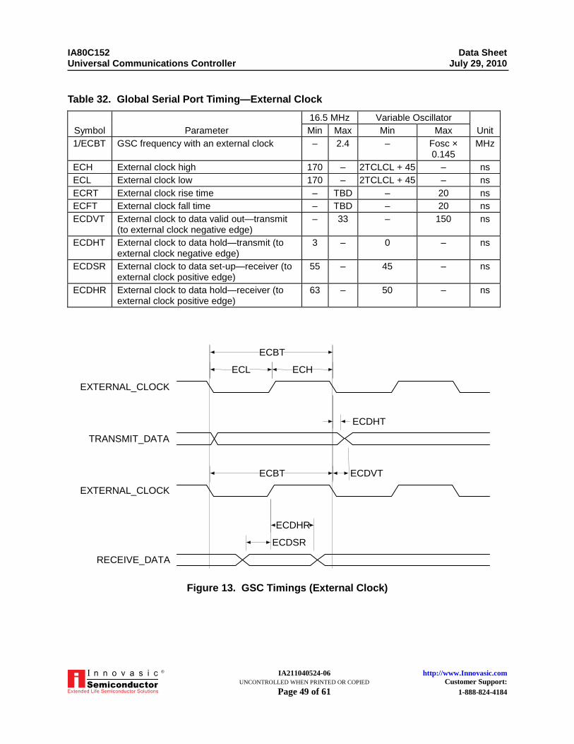
IA80C152 Data Sheet Universal Communications Controller July 29, 2010
IA211040524-06 http://www.Innovasic.com UNCONTROLLED WHEN PRINTED OR COPIED Customer Support: Page 49 of 61 1-888-824-4184
®
Table 32. Global Serial Port Timing—External Clock
Symbol Parameter
16.5 MHz Variable Oscillator
Unit Min Max Min Max
1/ECBT GSC frequency with an external clock – 2.4 – Fosc × 0.145
MHz
ECH External clock high 170 – 2TCLCL + 45 – ns
ECL External clock low 170 – 2TCLCL + 45 – ns
ECRT External clock rise time – TBD – 20 ns
ECFT External clock fall time – TBD – 20 ns
ECDVT External clock to data valid out—transmit (to external clock negative edge)
– 33 – 150 ns
ECDHT External clock to data hold—transmit (to external clock negative edge)
3 – 0 – ns
ECDSR External clock to data set-up—receiver (to external clock positive edge)
55 – 45 – ns
ECDHR External clock to data hold—receiver (to external clock positive edge)
63 – 50 – ns
Figure 13. GSC Timings (External Clock)
EXTERNAL_CLOCK
TRANSMIT_DATA
EXTERNAL_CLOCK
RECEIVE_DATA
ECBT
ECBT
ECL ECH
ECDHT
ECDVT
ECDSR
ECDHR
IA80C152 Data Sheet Universal Communications Controller July 29, 2010
IA211040524-06 http://www.Innovasic.com UNCONTROLLED WHEN PRINTED OR COPIED Customer Support: Page 50 of 61 1-888-824-4184
®
6. Instruction Set Summary Table
Table 33 provides a summary of the instruction set organized by hexadecimal opcode. Please
refer to the original Intel Data Book for individual instruction set details.
Table 33. Instruction Set Summary
Opcode Mnemonic
00 H NOP
01 H AJMP addr11
02 H LJMP addr16
03 H RR A
04 H INC A
05 H INC direct
06 H INC @R0
07 H INC @R1
08 H INC R0
09 H INC R1
0A H INC R2
0B H INC R3
0C H INC R4
0D H INC R5
0E H INC R6
0F H INC R7
10 H JBC bit,rel
11 H ACALL addr11
12 H LCALL addr16
13 H RRC A
14 H DEC A
15 H DEC direct
16 H DEC @R0
17 H DEC @R1
18 H DEC R0
19 H DEC R1
1A H DEC R2
1B H DEC R3
1C H DEC R4
1D H DEC R5
1E H DEC R6
1F H DEC R7
20 H JB bit.rel
21 H AJMP addr11
22 H RET
23 H RL A
24 H ADD A,#data
25 H ADD A,direct
26 H ADD A,@R0
27 H ADD A,@R1
28 H ADD A,R0
IA80C152 Data Sheet Universal Communications Controller July 29, 2010
IA211040524-06 http://www.Innovasic.com UNCONTROLLED WHEN PRINTED OR COPIED Customer Support: Page 51 of 61 1-888-824-4184
®
Table 33. Instruction Set Summary (Continued)
Opcode Mnemonic
29 H ADD A,R1
2A H ADD A,R2
2B H ADD A,R3
2C H ADD A,R4
2D H ADD A,R5
2E H ADD A,R6
2F H ADD A,R7
30 H JNB bit.rel
31 H ACALL addr11
32 H RETI
33 H RLC A
34 H ADDC A,#data
35 H ADDC A,direct
36 H ADDC A,@R0
37 H ADDC A,@R1
38 H ADDC A,R0
39 H ADDC A,R1
3A H ADDC A,R2
3B H ADDC A,R3
3C H ADDC A,R4
3D H ADDC A,R5
3E H ADDC A,R6
3F H ADDC A,R7
40 H JC rel
41 H AJMP addr11
42 H ORL direct,A
43 H ORL direct,#data
44 H ORL A,#data
45 H ORL A,direct
46 H ORL A,@R0
47 H ORL A,@R1
48 H ORL A,R0
49 H ORL A,R1
4A H ORL A,R2
4B H ORL A,R3
4C H ORL A,R4
4D H ORL A,R5
4E H ORL A,R6
4F H ORL A,R7
50 H JNC rel
51 H ACALL addr11
52 H ANL direct,A
53 H ANL direct,#data
54 H ANL A,#data
55 H ANL A,direct
56 H ANL A,@R0
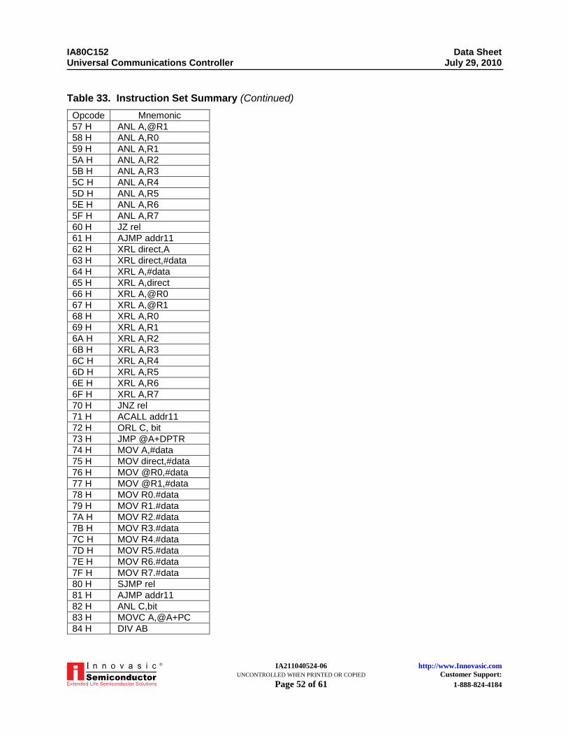
IA80C152 Data Sheet Universal Communications Controller July 29, 2010
IA211040524-06 http://www.Innovasic.com UNCONTROLLED WHEN PRINTED OR COPIED Customer Support: Page 52 of 61 1-888-824-4184
®
Table 33. Instruction Set Summary (Continued)
Opcode Mnemonic
57 H ANL A,@R1
58 H ANL A,R0
59 H ANL A,R1
5A H ANL A,R2
5B H ANL A,R3
5C H ANL A,R4
5D H ANL A,R5
5E H ANL A,R6
5F H ANL A,R7
60 H JZ rel
61 H AJMP addr11
62 H XRL direct,A
63 H XRL direct,#data
64 H XRL A,#data
65 H XRL A,direct
66 H XRL A,@R0
67 H XRL A,@R1
68 H XRL A,R0
69 H XRL A,R1
6A H XRL A,R2
6B H XRL A,R3
6C H XRL A,R4
6D H XRL A,R5
6E H XRL A,R6
6F H XRL A,R7
70 H JNZ rel
71 H ACALL addr11
72 H ORL C, bit
73 H JMP @A+DPTR
74 H MOV A,#data
75 H MOV direct,#data
76 H MOV @R0,#data
77 H MOV @R1,#data
78 H MOV R0.#data
79 H MOV R1.#data
7A H MOV R2.#data
7B H MOV R3.#data
7C H MOV R4.#data
7D H MOV R5.#data
7E H MOV R6.#data
7F H MOV R7.#data
80 H SJMP rel
81 H AJMP addr11
82 H ANL C,bit
83 H MOVC A,@A+PC
84 H DIV AB
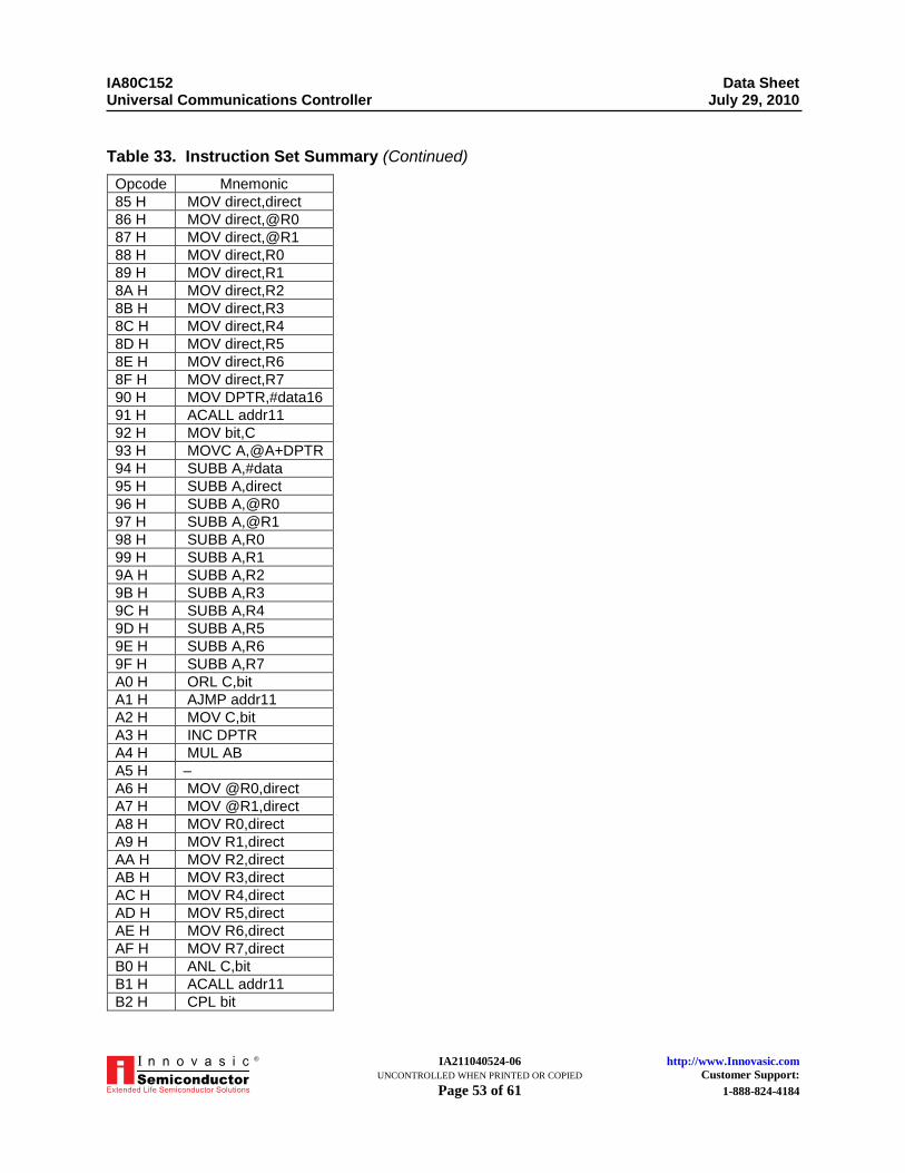
IA80C152 Data Sheet Universal Communications Controller July 29, 2010
IA211040524-06 http://www.Innovasic.com UNCONTROLLED WHEN PRINTED OR COPIED Customer Support: Page 53 of 61 1-888-824-4184
®
Table 33. Instruction Set Summary (Continued)
Opcode Mnemonic
85 H MOV direct,direct
86 H MOV direct,@R0
87 H MOV direct,@R1
88 H MOV direct,R0
89 H MOV direct,R1
8A H MOV direct,R2
8B H MOV direct,R3
8C H MOV direct,R4
8D H MOV direct,R5
8E H MOV direct,R6
8F H MOV direct,R7
90 H MOV DPTR,#data16
91 H ACALL addr11
92 H MOV bit,C
93 H MOVC A,@A+DPTR
94 H SUBB A,#data
95 H SUBB A,direct
96 H SUBB A,@R0
97 H SUBB A,@R1
98 H SUBB A,R0
99 H SUBB A,R1
9A H SUBB A,R2
9B H SUBB A,R3
9C H SUBB A,R4
9D H SUBB A,R5
9E H SUBB A,R6
9F H SUBB A,R7
A0 H ORL C,bit
A1 H AJMP addr11
A2 H MOV C,bit
A3 H INC DPTR
A4 H MUL AB
A5 H –
A6 H MOV @R0,direct
A7 H MOV @R1,direct
A8 H MOV R0,direct
A9 H MOV R1,direct
AA H MOV R2,direct
AB H MOV R3,direct
AC H MOV R4,direct
AD H MOV R5,direct
AE H MOV R6,direct
AF H MOV R7,direct
B0 H ANL C,bit
B1 H ACALL addr11
B2 H CPL bit
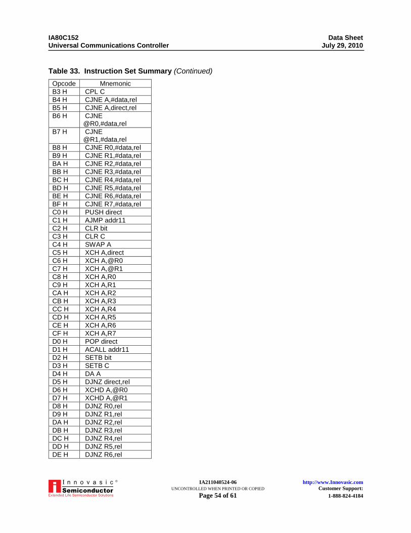
IA80C152 Data Sheet Universal Communications Controller July 29, 2010
IA211040524-06 http://www.Innovasic.com UNCONTROLLED WHEN PRINTED OR COPIED Customer Support: Page 54 of 61 1-888-824-4184
®
Table 33. Instruction Set Summary (Continued)
Opcode Mnemonic
B3 H CPL C
B4 H CJNE A,#data,rel
B5 H CJNE A,direct,rel
B6 H CJNE @R0,#data,rel
B7 H CJNE @R1,#data,rel
B8 H CJNE R0,#data,rel
B9 H CJNE R1,#data,rel
BA H CJNE R2,#data,rel
BB H CJNE R3,#data,rel
BC H CJNE R4,#data,rel
BD H CJNE R5,#data,rel
BE H CJNE R6,#data,rel
BF H CJNE R7,#data,rel
C0 H PUSH direct
C1 H AJMP addr11
C2 H CLR bit
C3 H CLR C
C4 H SWAP A
C5 H XCH A,direct
C6 H XCH A,@R0
C7 H XCH A,@R1
C8 H XCH A,R0
C9 H XCH A,R1
CA H XCH A,R2
CB H XCH A,R3
CC H XCH A,R4
CD H XCH A,R5
CE H XCH A,R6
CF H XCH A,R7
D0 H POP direct
D1 H ACALL addr11
D2 H SETB bit
D3 H SETB C
D4 H DA A
D5 H DJNZ direct,rel
D6 H XCHD A,@R0
D7 H XCHD A,@R1
D8 H DJNZ R0,rel
D9 H DJNZ R1,rel
DA H DJNZ R2,rel
DB H DJNZ R3,rel
DC H DJNZ R4,rel
DD H DJNZ R5,rel
DE H DJNZ R6,rel
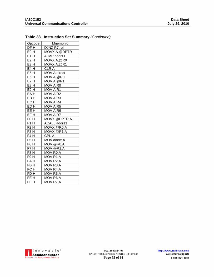
IA80C152 Data Sheet Universal Communications Controller July 29, 2010
IA211040524-06 http://www.Innovasic.com UNCONTROLLED WHEN PRINTED OR COPIED Customer Support: Page 55 of 61 1-888-824-4184
®
Table 33. Instruction Set Summary (Continued)
Opcode Mnemonic
DF H DJNZ R7,rel
E0 H MOVX A,@DPTR
E1 H AJMP addr11
E2 H MOVX A,@R0
E3 H MOVX A,@R1
E4 H CLR A
E5 H MOV A,direct
E6 H MOV A,@R0
E7 H MOV A,@R1
E8 H MOV A,R0
E9 H MOV A,R1
EA H MOV A,R2
EB H MOV A,R3
EC H MOV A,R4
ED H MOV A,R5
EE H MOV A,R6
EF H MOV A,R7
F0 H MOVX @DPTR,A
F1 H ACALL addr11
F2 H MOVX @R0,A
F3 H MOVX @R1,A
F4 H CPL A
F5 H MOV direct,A
F6 H MOV @R0,A
F7 H MOV @R1,A
F8 H MOV R0,A
F9 H MOV R1,A
FA H MOV R2,A
FB H MOV R3,A
FC H MOV R4,A
FD H MOV R5,A
FE H MOV R6,A
FF H MOV R7,A
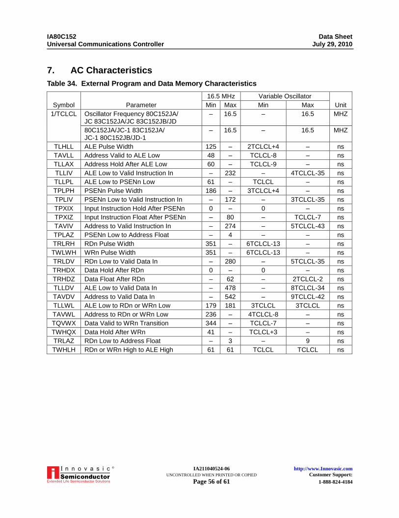
IA80C152 Data Sheet Universal Communications Controller July 29, 2010
IA211040524-06 http://www.Innovasic.com UNCONTROLLED WHEN PRINTED OR COPIED Customer Support: Page 56 of 61 1-888-824-4184
®
7. AC Characteristics
Table 34. External Program and Data Memory Characteristics
Symbol Parameter
16.5 MHz Variable Oscillator
Unit Min Max Min Max
1/TCLCL Oscillator Frequency 80C152JA/ JC 83C152JA/JC 83C152JB/JD
– 16.5 – 16.5 MHZ
80C152JA/JC-1 83C152JA/ JC-1 80C152JB/JD-1
– 16.5 – 16.5 MHZ
TLHLL ALE Pulse Width 125 – 2TCLCL+4 – ns
TAVLL Address Valid to ALE Low 48 – TCLCL-8 – ns
TLLAX Address Hold After ALE Low 60 – TCLCL-9 – ns
TLLIV ALE Low to Valid Instruction In – 232 – 4TCLCL-35 ns
TLLPL ALE Low to PSENn Low 61 – TCLCL – ns
TPLPH PSENn Pulse Width 186 – 3TCLCL+4 – ns
TPLIV PSENn Low to Valid Instruction In – 172 – 3TCLCL-35 ns
TPXIX Input Instruction Hold After PSENn 0 – 0 – ns
TPXIZ Input Instruction Float After PSENn – 80 – TCLCL-7 ns
TAVIV Address to Valid Instruction In – 274 – 5TCLCL-43 ns
TPLAZ PSENn Low to Address Float – 4 – – ns
TRLRH RDn Pulse Width 351 – 6TCLCL-13 – ns
TWLWH WRn Pulse Width 351 – 6TCLCL-13 – ns
TRLDV RDn Low to Valid Data In – 280 – 5TCLCL-35 ns
TRHDX Data Hold After RDn 0 – 0 – ns
TRHDZ Data Float After RDn – 62 – 2TCLCL-2 ns
TLLDV ALE Low to Valid Data In – 478 – 8TCLCL-34 ns
TAVDV Address to Valid Data In – 542 – 9TCLCL-42 ns
TLLWL ALE Low to RDn or WRn Low 179 181 3TCLCL 3TCLCL ns
TAVWL Address to RDn or WRn Low 236 – 4TCLCL-8 – ns
TQVWX Data Valid to WRn Transition 344 – TCLCL-7 – ns
TWHQX Data Hold After WRn 41 – TCLCL+3 – ns
TRLAZ RDn Low to Address Float – 3 – 9 ns
TWHLH RDn or WRn High to ALE High 61 61 TCLCL TCLCL ns
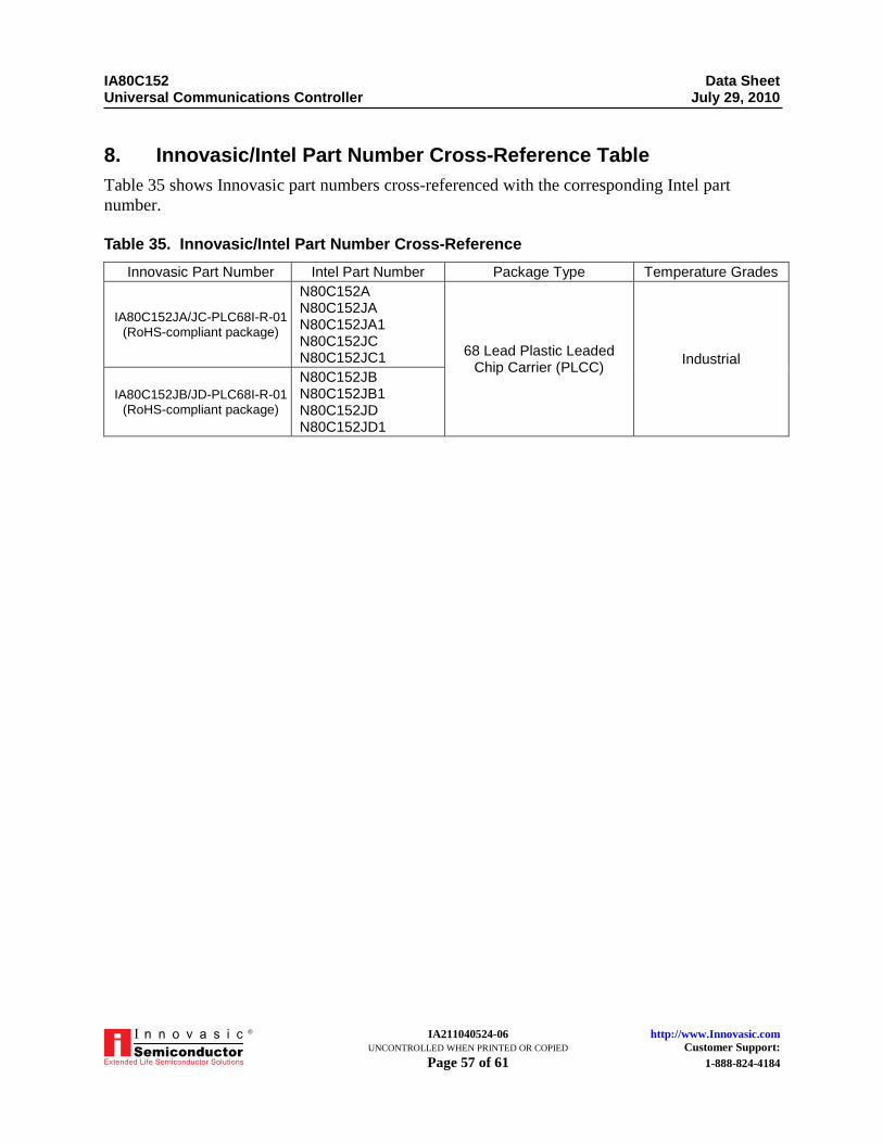
IA80C152 Data Sheet Universal Communications Controller July 29, 2010
IA211040524-06 http://www.Innovasic.com UNCONTROLLED WHEN PRINTED OR COPIED Customer Support: Page 57 of 61 1-888-824-4184
®
8. Innovasic/Intel Part Number Cross-Reference Table
Table 35 shows Innovasic part numbers cross-referenced with the corresponding Intel part
number.
Table 35. Innovasic/Intel Part Number Cross-Reference
Innovasic Part Number Intel Part Number Package Type Temperature Grades
IA80C152JA/JC-PLC68I-R-01 (RoHS-compliant package)
N80C152A N80C152JA N80C152JA1 N80C152JC N80C152JC1
68 Lead Plastic Leaded Chip Carrier (PLCC)
Industrial
IA80C152JB/JD-PLC68I-R-01 (RoHS-compliant package)
N80C152JB N80C152JB1 N80C152JD N80C152JD1
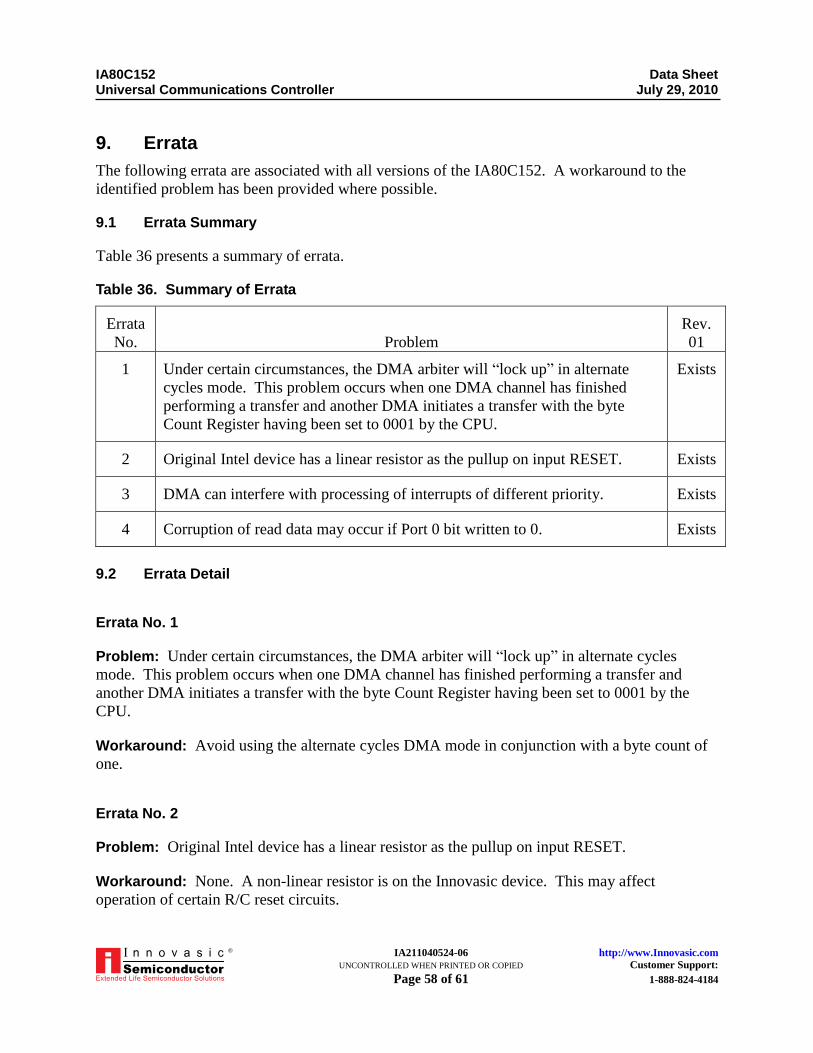
IA80C152 Data Sheet Universal Communications Controller July 29, 2010
IA211040524-06 http://www.Innovasic.com UNCONTROLLED WHEN PRINTED OR COPIED Customer Support: Page 58 of 61 1-888-824-4184
®
9. Errata
The following errata are associated with all versions of the IA80C152. A workaround to the
identified problem has been provided where possible.
9.1 Errata Summary
Table 36 presents a summary of errata.
Table 36. Summary of Errata
Errata
No. Problem
Rev.
01
1 Under certain circumstances, the DMA arbiter will ―lock up‖ in alternate
cycles mode. This problem occurs when one DMA channel has finished
performing a transfer and another DMA initiates a transfer with the byte
Count Register having been set to 0001 by the CPU.
Exists
2 Original Intel device has a linear resistor as the pullup on input RESET. Exists
3 DMA can interfere with processing of interrupts of different priority. Exists
4 Corruption of read data may occur if Port 0 bit written to 0. Exists
9.2 Errata Detail
Errata No. 1
Problem: Under certain circumstances, the DMA arbiter will ―lock up‖ in alternate cycles
mode. This problem occurs when one DMA channel has finished performing a transfer and
another DMA initiates a transfer with the byte Count Register having been set to 0001 by the
CPU.
Workaround: Avoid using the alternate cycles DMA mode in conjunction with a byte count of
one.
Errata No. 2
Problem: Original Intel device has a linear resistor as the pullup on input RESET.
Workaround: None. A non-linear resistor is on the Innovasic device. This may affect
operation of certain R/C reset circuits.
IA80C152 Data Sheet Universal Communications Controller July 29, 2010
IA211040524-06 http://www.Innovasic.com UNCONTROLLED WHEN PRINTED OR COPIED Customer Support: Page 59 of 61 1-888-824-4184
®
Errata No. 3
Problem: DMA can interfere with processing of interrupts of different priority.
Description: The following sequence of events must occur for this issue to occur:
1. A low-priority (associated priority bit not set) interrupt is accepted by the processor, but
vector fetch is delayed by a DMA cycle.
2. During DMA cycle, a high-priority (associated priority bit set) interrupt is accepted.
3. After DMA cycle, the high-priority vector is fetched. No further processing of any low-
priority interrupts will occur.
Workaround: Use inherent prioritization of interrupts (all interrupts set to high or low priority
only) if DMA is enabled.
Errata No. 4
Problem: Corruption of read data may occur if Port 0 bit written to 0.
Description: If any bit in Port 0 is written to a 0 while the device is configured to use P0 as
address/data bus, corruption of read data may occur.
Workaround: Write all Port 0 register bits to a 1 while using P0 as address/data bus.
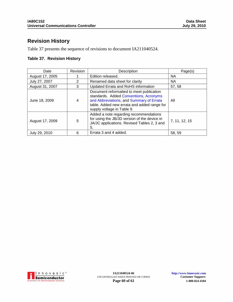
IA80C152 Data Sheet Universal Communications Controller July 29, 2010
IA211040524-06 http://www.Innovasic.com UNCONTROLLED WHEN PRINTED OR COPIED Customer Support: Page 60 of 61 1-888-824-4184
®
Revision History
Table 37 presents the sequence of revisions to document IA211040524.
Table 37. Revision History
Date Revision Description Page(s)
August 17, 2005 1 Edition released. NA
July 27, 2007 2 Renamed data sheet for clarity NA
August 31, 2007 3 Updated Errata and RoHS information 57, 58
June 18, 2009 4
Document reformatted to meet publication standards. Added Conventions, Acronyms and Abbreviations, and Summary of Errata table. Added new errata and added range for supply voltage in Table 9.
All
August 17, 2009 5
Added a note regarding recommendations for using the JB/JD version of the device in JA/JC applications. Revised Tables 2, 3 and 5.
7, 11, 12, 15
July 29, 2010 6 Errata 3 and 4 added. 58, 59
IA80C152 Data Sheet Universal Communications Controller July 29, 2010
IA211040524-06 http://www.Innovasic.com UNCONTROLLED WHEN PRINTED OR COPIED Customer Support: Page 61 of 61 1-888-824-4184
®
10. For Additional Information
The IA80C152 is a ―plug-and-play‖ drop-in replacement for the original Intel 80C152.
Innovasic produces replacement ICs using its MILES, or Managed IC Lifetime Extension
System, cloning technology. This technology produces replacement ICs far more complex than
―emulation‖ while ensuring they are compatible with the original IC. MILES captures the design
of a clone so it can be produced even as silicon technology advances. MILES also verifies the
clone against the original IC so that even the ―undocumented features‖ are duplicated. This data
sheet presents engineering information about the IA80C152 including functional and I/O
descriptions, electrical characteristics, and applicable timing.
The Innovasic Support Team wants its information to be complete, accurate, useful, and easy to
understand. Please feel free to contact experts at Innovasic with suggestions, comments, or
questions at any time.
Innovasic Support Team
3737 Princeton NE
Suite 130
Albuquerque, NM 87107
(505) 883-5263
Fax: (505) 883-5477
Toll Free: (888) 824-4184
E-mail: [email protected]
Website: http://www.Innovasic.com