Embed Size (px)
Citation preview


I hereby declare that I have read through this report entitle “A Study On Current Carrying
Capacity Of Single Layer PCB” and found that has comply the partial fulfilment for
awarding the degree of Bachelor of Electrical Engineering (Industrial Power).
Signature : ………………………..
Supervisor’s name : ………………………..
Date : ………………………..
A STUDY ON CURRENT CARRYING CAP A CITY OF SINGLE LAYER PCB
MUHAMMAD A'ZIM HAKIM BIN SHAHARBUDIN
A report submitted in partial fulf"illment of the requirements for the degree
of Electrical Engineering (Industrial Power)
Faculty of Electrical Engineering
UNJVERSITI TEKNIKAL MALAYSIA MELAKA
JUN2012


i
ACKNOWLEDGEMENT
I would like to take this opportunity to express my gratitude to all the parties that
have been assisting me throughout the duration of my final year project report.
First and foremost, I would like to shower a million thanks to my supervisor, Miss
Arfah Binti Ahmad who has been of outmost help and patience. From the first I was started
my final year project, until the end, she has been my source of motivation, inspiration, and
my guiding light. All the input toward the meeting with her has tremendously benefited me
in various aspects and kept in a corner of my mind at all times while developing this
project successfully.
Last but not least I would like to thank all my family members and friends who
have been extremely supportive throughout the duration of the entire project and helping
me to complete my final year project report.
ii
ABSTRACT
Realizing the increasing importance and demand of a single layer Printed Circuit
Board (PCB) in high current carrying capacity is subject of a closer research. This report
address on correlations between electrical current and temperature rise on PCB traces. A
temperature rise or thermal management is one on of the most important consideration on
PCB design that can brings damage to the board if the PCB traces is exposed to a higher
temperature than its limits. To prevent this problem, the period of erosion of copper track
of the PCB will be estimated from a series of analysis of temperature rise in a single layer
PCB. The relation between current and temperature rise in the copper trace of single layer
PCB with different width and condition of the trace will be determine. The aim of this
research is to determine a relation between current and temperature rise under performance
on PCB board. The method to perform this experiment is using current injection from
electrical device into PCB trace and the heat will be captured by using a FLIR thermal
imager. Finally, data obtained will be analyzed by using statistical approach.

iii
ABSTRAK
Projek ini berkaitan dengan mengkaji keupayaan pengaliran arus (CCC) bagi dua
lapisan papan litar bercetak (PCB) dengan menggunakan pendekatan statistik. Sejak
beberapa tahun kebelakangan ini, reka bentuk PCB seperti komputer riba telah menjadi
semakin padat dengan pengecilan saiz dan kepadatan elektronik. Oleh itu, ia adalah
penting untuk merekabentuk pengalir PCB bagi tujuan tersebut. Tujuan projek ini adalah
untuk menentukan faktor-faktor yang mempengaruhi keupayaan pengaliran arus dan
kelesapan haba serta hubungan antara pembolehubah-pembolehubah ini. Projek ini
tertumpu kepada dua lapisan PCB, arus masukan pada pengalir, kelebaran pengalir, dan
sudut pengalir. Faktor-faktor yang tetap pula adalah panjang pengalir dan suhu bilik. Untuk
reka bentuk PCB pula, perisian PCB Express digunakan untuk memudahkan dan
menjimatkan masa untuk proses mereka-bentuk kelebaran dan sudut pengalir yang diingini
dalam kajian ini. Selepas reka bentuk PCB telah dibuat, PCB tersebut akan menjalani
proses goresan untuk membuang pengalir-pengalir lebihan yang tidak digunakan atas
papan. Ketika eksperimen, arus akan dialirkan ke pengalir pada PCB. Selepas 10 minit,
suhu pada pengalir pada PCB akan stabil dan data akan diambil menggunakan FLIR
Thermal Imager. Untuk memastikan yang data adalah tepat, data perlulah diambil sebayak
5 kali untuk setiap pengalir pada PCB. Kenaikan suhu pengalir pada PCB adalah
disebabkan oleh beberapa parameter dan beberapa parameter juga tidak memberi kesan
kepada kenaikan suhu pengalir. Ia menghuraikan tentang hubung kait diantara arus elektrik
dan kenaikan suhu pengalir. Apabila terdapat kenaikan suhu disebabkan pengagihan dan
kelesapan haba semasa aliran arus yang melalui pengalir PCB, ini boleh menyebabkan
PCB gagal untuk beroperasi seperti biasa dan mengakibatkan kemusnahan bagi operasi
PCB.

iv
TABLE OF CONTENT
CHAPTER TITLE PAGE
ACKNOWLEDGEMENT I
ABSTRACT II
TABLE OF CONTENT IV
LIST OF FIGURES VI
LIST OF TABLES VII
1 INTRODUCTION 1
1.1 Background 1
1.2 Problem Statement 2
1.3 Project objective 3
1.4 Project scope 3
2 LITERATURE REVIEW 4
2.1 Introduction 5
2.2 Current Carrying Capacity 5
2.3 IPC (Interconnecting and Packaging Electronic Circuit) standard 8
2.4 Characterization of FR4 PCB 10
2.5 Thermal Design Guideline 11
2.5.1 Discussion on new design guideline 11
2.5.2 Corner effect 14
2.6 Literature review discussion 15
3 METHODOLOGY 16
3.1 Introduction 16
3.2 Methodology chart 16
3.2.1 Method 1: Find Source and Study 18
3.2.2 Method 2: Design PCB 18
3.2.3 Third step: Experiment and Data Captured 21

v
4 RESULT AND ANALYSIS 23
4.1 Introduction 23
4.2 Lab testing 23
4.2.1 Straight line trace 24
4.2.2 Bended corner trace 25
4.3 Simulate Data 26
4.4 Analysis of Current, ΔT and width for straight line 28
4.4.1 Model fitting test 28
4.4.2 Straight Line before improvement 29
4.4.3 Straight line after improvement 32
4.4.4 Model Accuracy 35
4.5 Analysis of Current, ΔT and width for bended corner 37
4.5.1 Bended corner before improvement 38
4.5.2 Bended corner after improvement 41
4.5.3 Model Accuracy 44
5 CONCLUSION AND RECOMMENDATION 45
5.1 Introduction 45
5.2 Conclusion 45
5.3 Recommendation 47
REFERENCE 48
6 APPENDIX 49

vi
LIST OF FIGURES
FIGURE TITLE PAGE
Figure 2.1 K-Chart Map 4
Figure 2.2 Infrared thermal imaging copper conductor 7
Figure 2.3 Conductor width to cross-section relationship 8
Figure 2.4 Flaw in IPC Standard 9
Figure 2.5 A Portion of board used in IPC-TM650 12
Figure 2.6 Heat transferred in Single Layer and Double layer [6] 13
Figure 2.7 Proposed test board configuration for bended traces with round corner 14
Figure 3.1 Methodology Flow Chart 17
Figure 3.2 PCB design printed on tracing paper 19
Figure 3.3 Exposed the PCB to UV ray 19
Figure 3.4 Copper trace after etching process 20
Figure 3.5 The set-up experiment 21
Figure 3.6 Dual-Tracking DC Power Supply 22
Figure 3.7 FLIR i5 thermal imager 22
Figure 4.1 Result of 1A Single Line 24
Figure 4.2 Result of 3A Bended Corner 25
Figure 4.3 3D Graph for Straight Line 27
Figure 4.4 Regression Analysis for straight line 29
Figure 4.5 Normal probability plot of residual 31
Figure 4.6 Regression Analysis for straight line after improvement 32
Figure 4.7 Normal probability plot of residual after improvement 34
Figure 4.8 Current Estimation Graph 36
Figure 4.9 3D surface plot for bended corner 37
Figure 4.10 Minitab output for bended corner before improvement 38
Figure 4.11 Normal probability plot of bended corner before improvement 40
Figure 4.12 Minitab output for bended corner after improvement 41
Figure 4.13 Normal probability plot after improvement 43
Figure 4.14 Estimation current with valid data 44

vii
LIST OF TABLES
TABLE TITLE PAGE
Table 2.1 Some of the common PCB material types 10
Table 2.2 Measured Temperature of Trace on PCB with M=0 and M=40mm[6] 12
Table 4.1 Data with Current Estimation 35

1
1 CHAPTER 1
INTRODUCTION
1.1 Background
In recent years, the design of Printed Circuit Board (PCB) current carrying capacity
such as personal computer (PC) has become increasingly dense with miniaturization of
electronic packaging. At the same time, the speed of a digital electronic device used
increase make more electrical current must be delivered to the device, typically via a PCB.
This imposes certain limitation and critical requirement. Multi-media portable device such
as hand phone and tablet phone which comes with less weight and smaller size is
increasing the demand and provides an extra problem for PCB design.
Thermal management is one of the most important considerations in PCB design.
The heat is distributed and dissipated during current flow which may potentially result in
PCB fail to operate normally. This situation requires scheduled preventive maintenance
activities as well as high operation cost. By predicting the temperature rise on the current
carrying capacity of PCB, a failure on the PCB or malfunction of an electronic device can
be minimized.
Prediction of the temperature rise on the PCB involves an experiment and
calculations. Constructing the prototype PCB and performing an experiment with the
prototype board in a laboratory is the best and most accurate method, but result in time
consuming and money costly. However, to obtained data sometimes it is restricted for
certain design of PCB and required a repeated experiment with different PCB design.
Thus, other design alternatives which also inexpensive and less time consuming should be
employed.
2
One of the alternative methods is by using statistical approach such as data analysis
technique. This technique generally requires complete parameters to obtain a perfect
solution. For problem of temperature rise on PCB which involving a complex geometries,
loading and material properties, it is generally not possible to obtain a solution using this
method. Beside, this method is valid for infinite number of location on the PCB. Hence, it
is required to employ alternate method which is data analysis technique such as linear
regression analysis.
1.2 Problem Statement
According to Institute for Interconnecting and Packaging Electronic Circuits (IPC)
standard, the current carrying capacity of PCB traces represent the maximum electrical
current that can be carried continuously by a trace without causing an objectionable
degradation of electrical or mechanical properties of the devices. When current flowing
through the copper trace and the current will generates heat in the copper will causes a
deposition of thermal energy in that copper. The heat then will create a temperature rise
between the trace and the surrounding environment (others microelectronic components).
Hence, if the trace is exposed to a higher temperature than its limitation, the PCB could
damage or worst case the PCB will explode and the electronic device will be caught on
fire. This happen because the heat from the copper traces is not dissipated properly from
the copper traces itself.
However, the relationship between current and temperature rise in PCB just not
depend on the trace copper. There are a lot more variable that may have a significant
impact on the PCB current carrying capacity. Some of those variables are PCB size and
thickness, number of traces that are involved in current carrying, trace separation, presence
or absence of the ground and/or power copper lane and system cooling condition. Only a
few variables will be studying the relationship between current and temperature rise such
as single layer PCB, copper width and straight or bended corner line. This parameter is one
of the problems for the industrial because PCB is widely used in all electrical devices with
high current carrying capacity flow through the PCB board. As the problem keep remains
exist there should be solutions on how to determine the best temperature for PCB board.

3
1.3 Project objective
There are three objectives that need to be achieved to complete this project which are
1) To study current distribution and heat dissipation of current carrying capacity.
2) To build a PCB board for data collection.
3) To develop statistical equation for modelling ideal temperature on PCB.
1.4 Project scope
This study focuses only on a single layer PCB. The base material of the board is
FR4 Glass-Epoxy Single Sided. The size of the board is 150mm (width) x 300mm (length).
The trace spacing of the copper is not fixed with the other copper traces. According to the
journal by Mike Jouppi’s on his journal regarding current carrying capacity. Literally, there
are two types of parameters that are identified to get the relationship between current and
temperature rise.
The parameters are copper trace and trace condition which straight line or bended
corner. The copper width that has been investigating is 0.06 inch, 0.08 inch and 0.10 inch.
As the bended corner is about 110°, 130° and 150°. The current ranging from 0-5 Ampere
was injected to each trace line and bended copper. Thus, the selected injected current has
been decided is 1A, 3A and 5A to get a better result and easy to analysis the data. The data
which had obtained from the experiment was analyzed using statistical software which is
Minitab.

4
2 CHAPTER 2
LITERATURE REVIEW
Figure 2.1 K-Chart Map
Current Carrying Capacity
Printed Circuit Board
Single Layer
Double Layer
Size
Thickness
Copper
Copper Width
Copper Trace
Number Of Trace
Trace Condition
Straight Corner
Thermal Management

5
2.1 Introduction
This chapter highlight the past studies related to this project and background
theory.
2.2 Current Carrying Capacity
Thermal management is an important design consideration in modern electronic
packaging according to a journal written by Tsung-Yu Pan titled “Current Carrying of
Copper Conductors in printed Wiring Boards” [1]. The author state that the requirement of
the current carrying capacity of copper conductors on the surface of a printed wiring board
due to temperature rise has not been studied thoroughly since the generic handbook data
being published. In this journal, the author discuss more about the effect of thermal
management of the copper conductors on Printed Wiring Board (PWB) or what they called
now is Printed Circuit Board (PCB) having a different dimensions and arrangement. The
author also stated that the experiment is used an infrared thermal as experiment basis. Then
finite element analysis will be applied to correlate temperature rise versus conductor
dimension and spacing, current amount and board dimensions.
Thermal resistance, Rt, has been widely used to described the thermal characteristic
of electronic packaging. Rt is defined as:
(2.1)
where ΔT = temperature increase in °C,
Q = heat flow rate in Watt,
Rt = thermal resistance in °C/Watt, which is a parameter analogous to
electrical resistance.

6
To consider the heat management of copper conductor, a heat sink is not often
considered because a copper conductor is usually having a big effect to PCB. So Rt is a
combination of
i. Conduction through the board.
ii. Free air convection near the conductor and board surface
iii. Radiation into the surrounding component.
The heat flow, Q for the copper conductor is provided by an electrical current flow
through the conductor. Q is proportional to current I and resistance Re.
(2.2)
where I = current in ampere,
Re = electric resistance in Ω
(2.3)
where Ρ = electric resistivity in Ω-mm,
ℓ = length of the conductor in mm,
t = thickness of the conductor in mm,
w = width of the conductor in mm.
Therefore, (2.4)

7
Figure 2.2 shows the temperature distribution on the PCB board surface across the
conductor with current range of 1 to 3 ampere. It shows that thermal resistance Rt is not
constant throughout the whole temperature range. This is because to the fact that Rt is a
combination of conduction, free convection and radiation. Basically conduction through
the board is always constant for different ambient temperature.
Figure 2.2 Infrared thermal imaging copper conductor

8
2.3 IPC (Interconnecting and Packaging Electronic Circuit) standard
The first standard chart that is often referred to is IPC 2152 performed by the
National Bureau of Standards in 1956 [2]. According to the journal, this standard was
established when printed circuit industry was in its infancy and when a guide for sizing
conductor was first required. The original charts were developed from two different board
materials, primarily XXXP (phenolic) and epoxy. These boards were 1/16 and 1/32 inch
thick, had ½ oz, 1 oz, 2 oz and 3 oz copper conductor and some of the board had copper
plane on one side of the board. The first parameters that been investigated by IPC are
board material property, board thickness, copper weight and copper plane were influence
trace temperature [2].
Figure 2.3 Conductor width to cross-section relationship
9
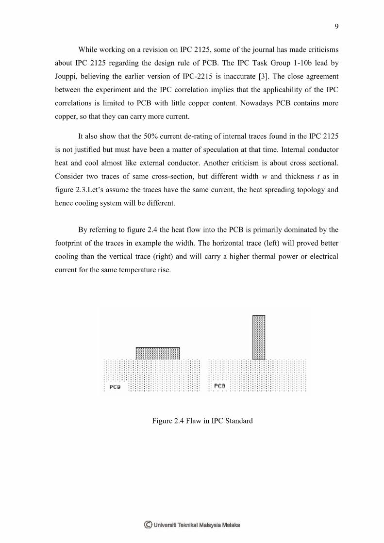
While working on a revision on IPC 2125, some of the journal has made criticisms
about IPC 2125 regarding the design rule of PCB. The IPC Task Group 1-10b lead by
Jouppi, believing the earlier version of IPC-2215 is inaccurate [3]. The close agreement
between the experiment and the IPC correlation implies that the applicability of the IPC
correlations is limited to PCB with little copper content. Nowadays PCB contains more
copper, so that they can carry more current.
It also show that the 50% current de-rating of internal traces found in the IPC 2125
is not justified but must have been a matter of speculation at that time. Internal conductor
heat and cool almost like external conductor. Another criticism is about cross sectional.
Consider two traces of same cross-section, but different width w and thickness t as in
figure 2.3.Let’s assume the traces have the same current, the heat spreading topology and
hence cooling system will be different.
By referring to figure 2.4 the heat flow into the PCB is primarily dominated by the
footprint of the traces in example the width. The horizontal trace (left) will proved better
cooling than the vertical trace (right) and will carry a higher thermal power or electrical
current for the same temperature rise.
Figure 2.4 Flaw in IPC Standard
10
2.4 Characterization of FR4 PCB
Based on the literature review, there have been few attempted studies that were
conducted on characterizing certain types of FR-4 laminates and assessing the impact of
lead-free soldering assembly conditions on reliability of printed circuit boards. To date, no
comprehensive report is available on the effect of lead-free soldering exposures on
laminate material properties. Furthermore, a wide variety of laminate types that are
commercialized as ‘Lead-free process compatible’ are available recently and selection of
appropriate laminates has been a challenge for the electronic industry.
An insight into the laminate material constituents and variations in their material
properties due to lead-free soldering exposures is essential in the selection of appropriate
laminate materials. The broad objective is to characterize a wide range of commercially
available FR-4 PCB laminate materials and investigate the effects of lead-free processing
on the thermo mechanical, physical, and chemical properties. The analysis is aimed at
correlating the properties to the material constituents of laminates [4].
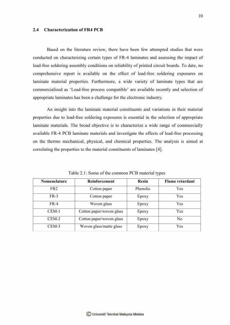
Table 2.1: Some of the common PCB material types
Nomenclature Reinforcement Resin Flame retardant
FR2 Cotton paper Phenolic Yes
FR-3 Cotton paper Epoxy Yes
FR-4 Woven glass Epoxy Yes
CEM-1 Cotton paper/woven glass Epoxy Yes
CEM-2 Cotton paper/woven glass Epoxy No
CEM-3 Woven glass/matte glass Epoxy Yes

11
2.5 Thermal Design Guideline
A thermal design guideline which is able to reliably predict the current carrying
capacity (CCC) of PCB trace will be a valuable to PCB engineer. Thus, according to YI
Wang [5] in her paper describes several design guidelines for the trace CCC. YI Wang also
mention some of limitation to PCB design characterized dense component and high current
applied to today’s PCB. Hence, the new methods for developing a new design guidelines
which are more efficient for today’s PCB design has been introduced. As mention in the
second review before, many experiment and research on PCB copper trace, thermal
management has been done by referring to the IPC standard and IPC has come up with
IPC-2125 which is expected to be more precise and comprehensive guideline in
determining PCB design. The differences between YI Wang PCB design and IPC-2125
design, which is has a flaw on designing PCB are:
1) All guidelines are based on PCB with large area space. This can hardly be found in
today’s PCB
2) Single layer, multi-layers, trace corner, copper width is prevalent in PCB with more
component density and high current density.
2.5.1 Discussion on new design guideline
All those guidelines gradually improved on the reliability and applicability of PCB
design but none dwell on the fact that modern PCB has limited bare space. In practical,
trace spacing (D) is much less than 30.5mm and sometimes less that 1mm [5].
1) To create a new standard for CCC on PCB board
2) To formulate a new PCB trace thermal design guideline which is applicable and
reliable for high power density
3) The influence of single and multi layer
4) The corner effect on current carrying capacity
5) Methods for temperature measurement
12
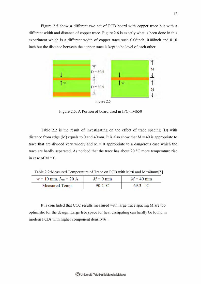
Figure 2.5 show a different two set of PCB board with copper trace but with a
different width and distance of copper trace. Figure 2.6 is exactly what is been done in this
experiment which is a different width of copper trace such 0.06inch, 0.08inch and 0.10
inch but the distance between the copper trace is kept to be level of each other.
Figure 2.5
Figure 2.5: A Portion of board used in IPC-TM650
Table 2.2 is the result of investigating on the effect of trace spacing (D) with
distance from edge (M) equals to 0 and 40mm. It is also show that M = 40 is appropriate to
trace that are divided very widely and M = 0 appropriate to a dangerous case which the
trace are hardly separated. As noticed that the trace has about 20 °C more temperature rise
in case of M = 0.
Table 2.2:Measured Temperature of Trace on PCB with M=0 and M=40mm[5]
It is concluded that CCC results measured with large trace spacing M are too
optimistic for the design. Large free space for heat dissipating can hardly be found in
modern PCBs with higher component density[6].