Embed Size (px)
Citation preview
Hybrid Memory Cube Specification 1.0
©2013 Altera Corporation, ARM Ltd., Hewlett-Packard Company, International Business Machines Corporation, Micron Technology, Inc., Open-Silicon, Inc., Samsung Electronics Co., Ltd., SK Hynix, Inc., and Xilinx, Inc.
All rights reserved. Hybrid Memory Cube Consortium
Hybrid Memory CubeHMC Memory Features
Hybrid Memory Cube
HMC Memory Features• Configured with independent memory vaults• Built-in memory controller for each vault
– Automatic refresh control over all temperatures• Internal ECC data correction• Advanced RAS features including data scrubbing• Post-assembly repair capability• In-field repair for ultimate reliability
HMC Interface Features• 10 Gbps, 12.5 Gbps, or 15 Gbps SerDes I/O interface• Multiple 16-lane, full-duplex serialized links
– Half-width link (8-lane) configuration also sup-ported
• Packet-based data/command interface• Supports 16, 32, 48, 64, 80, 96, 112, and 128 byte
references per request• Error detection (cyclic redundancy check [CRC]) for
packets with automatic retry• Power management supported per link• Through-silicon via (TSV) technology• Built-in self-test (BIST)• JTAG interface (IEEE 1149.1-2001, 1149.6)
©2012 Altera Corporation, ARM Ltd., Hewlett-Packard CompTechnology, Inc., Open-Silicon, Inc., Samsung Electronics Co., Lt
Hybrid Memory Cube Con
PDF: 09005aef84936aaf/Source: 09005aef84936abbhmc_gen2_hmcc_1.fm - Rev. 1.0 1/13 EN 1
DescriptionA hybrid memory cube (HMC) is a single package con-taining multiple memory die and one logic die, all stacked together using through-silicon via (TSV) tech-nology.
Scope of Specification• Section 1: HMC Architecture Overview• Sections 2-16: Common Protocol• Section 17-19: Electrical and Physical Link
Specifications for HMC-15G-SR (short reach)• Section 20-21: Electrical and Physical Link
Specifications for HMC-10G-USR (ultra short reach)
any, International Business Machines Corporation, Micron d., SK Hynix, Inc., and Xilinx, Inc. All rights reserved. sortium
The Hybrid Memory Cube Consortium reserves the right to change specifications without notice.
Hybrid Memory CubeTable of Contents
Table of Contents1 HMC Architecture . . . . . . . . . . . . . . . . . . . . . . . . . . . . . . . . . . . . . . . . . . . . . . . . . . . . . . . . . . . . . . . . . . . . . . . . . . . . . . . . . . .8
1.1 HMC Architecture . . . . . . . . . . . . . . . . . . . . . . . . . . . . . . . . . . . . . . . . . . . . . . . . . . . . . . . . . . . . . . . . . . . . . . . . . . . . . . .81.2 Logic Base Architecture . . . . . . . . . . . . . . . . . . . . . . . . . . . . . . . . . . . . . . . . . . . . . . . . . . . . . . . . . . . . . . . . . . . . . . . . . .9
2 Pin Descriptions . . . . . . . . . . . . . . . . . . . . . . . . . . . . . . . . . . . . . . . . . . . . . . . . . . . . . . . . . . . . . . . . . . . . . . . . . . . . . . . . . . .113 Link Data Transmission. . . . . . . . . . . . . . . . . . . . . . . . . . . . . . . . . . . . . . . . . . . . . . . . . . . . . . . . . . . . . . . . . . . . . . . . . . . . .134 Logical Sub-Block of Physical Layer . . . . . . . . . . . . . . . . . . . . . . . . . . . . . . . . . . . . . . . . . . . . . . . . . . . . . . . . . . . . . . . . . .14
4.1 Link Serialization. . . . . . . . . . . . . . . . . . . . . . . . . . . . . . . . . . . . . . . . . . . . . . . . . . . . . . . . . . . . . . . . . . . . . . . . . . . . . . .144.2 Scrambling and Descrambling. . . . . . . . . . . . . . . . . . . . . . . . . . . . . . . . . . . . . . . . . . . . . . . . . . . . . . . . . . . . . . . . . . .154.3 Lane Run Length Limitation. . . . . . . . . . . . . . . . . . . . . . . . . . . . . . . . . . . . . . . . . . . . . . . . . . . . . . . . . . . . . . . . . . . . .174.4 Lane Reversal . . . . . . . . . . . . . . . . . . . . . . . . . . . . . . . . . . . . . . . . . . . . . . . . . . . . . . . . . . . . . . . . . . . . . . . . . . . . . . . . . .184.5 Lane Polarity . . . . . . . . . . . . . . . . . . . . . . . . . . . . . . . . . . . . . . . . . . . . . . . . . . . . . . . . . . . . . . . . . . . . . . . . . . . . . . . . . .18
5 Chaining . . . . . . . . . . . . . . . . . . . . . . . . . . . . . . . . . . . . . . . . . . . . . . . . . . . . . . . . . . . . . . . . . . . . . . . . . . . . . . . . . . . . . . . . . .196 Power-On and Initialization . . . . . . . . . . . . . . . . . . . . . . . . . . . . . . . . . . . . . . . . . . . . . . . . . . . . . . . . . . . . . . . . . . . . . . . . .217 Power State Management . . . . . . . . . . . . . . . . . . . . . . . . . . . . . . . . . . . . . . . . . . . . . . . . . . . . . . . . . . . . . . . . . . . . . . . . . . .248 Link Layer . . . . . . . . . . . . . . . . . . . . . . . . . . . . . . . . . . . . . . . . . . . . . . . . . . . . . . . . . . . . . . . . . . . . . . . . . . . . . . . . . . . . . . . . .279 Transaction Layer . . . . . . . . . . . . . . . . . . . . . . . . . . . . . . . . . . . . . . . . . . . . . . . . . . . . . . . . . . . . . . . . . . . . . . . . . . . . . . . . . .28
9.1 Memory Addressing . . . . . . . . . . . . . . . . . . . . . . . . . . . . . . . . . . . . . . . . . . . . . . . . . . . . . . . . . . . . . . . . . . . . . . . . . . . .299.1.1 Memory Addressing Granularity . . . . . . . . . . . . . . . . . . . . . . . . . . . . . . . . . . . . . . . . . . . . . . . . . . . . . . . . . . . . .309.1.2 Memory Address-to-Link Mapping . . . . . . . . . . . . . . . . . . . . . . . . . . . . . . . . . . . . . . . . . . . . . . . . . . . . . . . . . .309.1.3 Default Address-Map Mode Table – 4-link Devices . . . . . . . . . . . . . . . . . . . . . . . . . . . . . . . . . . . . . . . . . . . .329.1.4 Default Address-Map Mode Table – 8-link Devices . . . . . . . . . . . . . . . . . . . . . . . . . . . . . . . . . . . . . . . . . . . .339.1.5 Address Mapping Mode Register. . . . . . . . . . . . . . . . . . . . . . . . . . . . . . . . . . . . . . . . . . . . . . . . . . . . . . . . . . . . .349.1.6 DRAM Addressing. . . . . . . . . . . . . . . . . . . . . . . . . . . . . . . . . . . . . . . . . . . . . . . . . . . . . . . . . . . . . . . . . . . . . . . . . .34
9.2 Packet Length. . . . . . . . . . . . . . . . . . . . . . . . . . . . . . . . . . . . . . . . . . . . . . . . . . . . . . . . . . . . . . . . . . . . . . . . . . . . . . . . . .349.3 Packet Flow Control . . . . . . . . . . . . . . . . . . . . . . . . . . . . . . . . . . . . . . . . . . . . . . . . . . . . . . . . . . . . . . . . . . . . . . . . . . . .359.4 Tagging . . . . . . . . . . . . . . . . . . . . . . . . . . . . . . . . . . . . . . . . . . . . . . . . . . . . . . . . . . . . . . . . . . . . . . . . . . . . . . . . . . . . . . .359.5 Packet Integrity . . . . . . . . . . . . . . . . . . . . . . . . . . . . . . . . . . . . . . . . . . . . . . . . . . . . . . . . . . . . . . . . . . . . . . . . . . . . . . . .369.6 Request Packets. . . . . . . . . . . . . . . . . . . . . . . . . . . . . . . . . . . . . . . . . . . . . . . . . . . . . . . . . . . . . . . . . . . . . . . . . . . . . . . .37
9.6.1 Request Header Layout . . . . . . . . . . . . . . . . . . . . . . . . . . . . . . . . . . . . . . . . . . . . . . . . . . . . . . . . . . . . . . . . . . . . .379.6.2 Request Tail Layout . . . . . . . . . . . . . . . . . . . . . . . . . . . . . . . . . . . . . . . . . . . . . . . . . . . . . . . . . . . . . . . . . . . . . . . .38
9.7 Response Packets . . . . . . . . . . . . . . . . . . . . . . . . . . . . . . . . . . . . . . . . . . . . . . . . . . . . . . . . . . . . . . . . . . . . . . . . . . . . . .389.8 Flow Packets. . . . . . . . . . . . . . . . . . . . . . . . . . . . . . . . . . . . . . . . . . . . . . . . . . . . . . . . . . . . . . . . . . . . . . . . . . . . . . . . . . .439.9 Poisoned Packets. . . . . . . . . . . . . . . . . . . . . . . . . . . . . . . . . . . . . . . . . . . . . . . . . . . . . . . . . . . . . . . . . . . . . . . . . . . . . . .439.10 Request Commands . . . . . . . . . . . . . . . . . . . . . . . . . . . . . . . . . . . . . . . . . . . . . . . . . . . . . . . . . . . . . . . . . . . . . . . . . . .44
9.10.1 READ and WRITE Request Commands . . . . . . . . . . . . . . . . . . . . . . . . . . . . . . . . . . . . . . . . . . . . . . . . . . . . . .459.10.2 POSTED WRITE Request Commands . . . . . . . . . . . . . . . . . . . . . . . . . . . . . . . . . . . . . . . . . . . . . . . . . . . . . . .459.10.3 ATOMIC Request Commands . . . . . . . . . . . . . . . . . . . . . . . . . . . . . . . . . . . . . . . . . . . . . . . . . . . . . . . . . . . . . .45
9.10.3.1 Dual 8-Byte Add Immediate. . . . . . . . . . . . . . . . . . . . . . . . . . . . . . . . . . . . . . . . . . . . . . . . . . . . . . . . . . . .469.10.3.2 Single 16-Byte Add Immediate . . . . . . . . . . . . . . . . . . . . . . . . . . . . . . . . . . . . . . . . . . . . . . . . . . . . . . . . .46
9.10.4 MODE READ and WRITE Request Commands . . . . . . . . . . . . . . . . . . . . . . . . . . . . . . . . . . . . . . . . . . . . . . .479.10.5 BIT WRITE Command . . . . . . . . . . . . . . . . . . . . . . . . . . . . . . . . . . . . . . . . . . . . . . . . . . . . . . . . . . . . . . . . . . . . .47
9.11 Response Commands . . . . . . . . . . . . . . . . . . . . . . . . . . . . . . . . . . . . . . . . . . . . . . . . . . . . . . . . . . . . . . . . . . . . . . . . .489.11.1 READ and MODE READ Response Command. . . . . . . . . . . . . . . . . . . . . . . . . . . . . . . . . . . . . . . . . . . . . . . .489.11.2 WRITE and MODE WRITE Response Command. . . . . . . . . . . . . . . . . . . . . . . . . . . . . . . . . . . . . . . . . . . . . .499.11.3 ERROR Response Command . . . . . . . . . . . . . . . . . . . . . . . . . . . . . . . . . . . . . . . . . . . . . . . . . . . . . . . . . . . . . . .49
9.12 Flow Commands . . . . . . . . . . . . . . . . . . . . . . . . . . . . . . . . . . . . . . . . . . . . . . . . . . . . . . . . . . . . . . . . . . . . . . . . . . . . . .499.12.1 NULL Command. . . . . . . . . . . . . . . . . . . . . . . . . . . . . . . . . . . . . . . . . . . . . . . . . . . . . . . . . . . . . . . . . . . . . . . . . .509.12.2 RETRY POINTER RETURN (PRET) Command. . . . . . . . . . . . . . . . . . . . . . . . . . . . . . . . . . . . . . . . . . . . . . . .509.12.3 TOKEN RETURN (TRET) Command . . . . . . . . . . . . . . . . . . . . . . . . . . . . . . . . . . . . . . . . . . . . . . . . . . . . . . . .509.12.4 INIT RETRY (IRTRY) Command . . . . . . . . . . . . . . . . . . . . . . . . . . . . . . . . . . . . . . . . . . . . . . . . . . . . . . . . . . . .50
9.13 Valid Field Command Summary . . . . . . . . . . . . . . . . . . . . . . . . . . . . . . . . . . . . . . . . . . . . . . . . . . . . . . . . . . . . . . . .50
PDF: 09005aef84936aaf/Source: 09005aef84936abb The Hybrid Memory Cube Consortium reserves the right to change specifications without notice.hmc_gen2_TOC.fm - Rev. 1.0 1/13 EN 2
Hybrid Memory CubeTable of Contents
9.14 Transaction Layer Initialization. . . . . . . . . . . . . . . . . . . . . . . . . . . . . . . . . . . . . . . . . . . . . . . . . . . . . . . . . . . . . . . . .5110 Configuration and Status Registers. . . . . . . . . . . . . . . . . . . . . . . . . . . . . . . . . . . . . . . . . . . . . . . . . . . . . . . . . . . . . . . . . .5211 Link Retry . . . . . . . . . . . . . . . . . . . . . . . . . . . . . . . . . . . . . . . . . . . . . . . . . . . . . . . . . . . . . . . . . . . . . . . . . . . . . . . . . . . . . . . .61
11.1 Retry Pointer Description . . . . . . . . . . . . . . . . . . . . . . . . . . . . . . . . . . . . . . . . . . . . . . . . . . . . . . . . . . . . . . . . . . . . . .6211.2 Link Master Retry Functions . . . . . . . . . . . . . . . . . . . . . . . . . . . . . . . . . . . . . . . . . . . . . . . . . . . . . . . . . . . . . . . . . . .63
11.2.1 Forward Retry Pointer Generation . . . . . . . . . . . . . . . . . . . . . . . . . . . . . . . . . . . . . . . . . . . . . . . . . . . . . . . . . .6411.2.2 Packet Sequence Number Generation . . . . . . . . . . . . . . . . . . . . . . . . . . . . . . . . . . . . . . . . . . . . . . . . . . . . . . .6411.2.3 Forward Retry Pointer Reception and Embedding . . . . . . . . . . . . . . . . . . . . . . . . . . . . . . . . . . . . . . . . . . . .6511.2.4 Return Retry Pointer Reception. . . . . . . . . . . . . . . . . . . . . . . . . . . . . . . . . . . . . . . . . . . . . . . . . . . . . . . . . . . . .6511.2.5 Link Master Sequences . . . . . . . . . . . . . . . . . . . . . . . . . . . . . . . . . . . . . . . . . . . . . . . . . . . . . . . . . . . . . . . . . . . .65
11.2.5.1 StartRetry Sequence. . . . . . . . . . . . . . . . . . . . . . . . . . . . . . . . . . . . . . . . . . . . . . . . . . . . . . . . . . . . . . . . . . .6511.2.5.2 LinkRetry Sequence . . . . . . . . . . . . . . . . . . . . . . . . . . . . . . . . . . . . . . . . . . . . . . . . . . . . . . . . . . . . . . . . . . .67
11.3 Link Slave Retry Functions . . . . . . . . . . . . . . . . . . . . . . . . . . . . . . . . . . . . . . . . . . . . . . . . . . . . . . . . . . . . . . . . . . . . .6911.3.1 Packet CRC/Sequence Check. . . . . . . . . . . . . . . . . . . . . . . . . . . . . . . . . . . . . . . . . . . . . . . . . . . . . . . . . . . . . . .69
11.3.1.1 FRP and RRP Extraction . . . . . . . . . . . . . . . . . . . . . . . . . . . . . . . . . . . . . . . . . . . . . . . . . . . . . . . . . . . . . . .6911.3.2 Error Abort Mode . . . . . . . . . . . . . . . . . . . . . . . . . . . . . . . . . . . . . . . . . . . . . . . . . . . . . . . . . . . . . . . . . . . . . . . . .6911.3.3 IRTRY Packet Operation . . . . . . . . . . . . . . . . . . . . . . . . . . . . . . . . . . . . . . . . . . . . . . . . . . . . . . . . . . . . . . . . . . .6911.3.4 Resumption of Normal Packet Stream after the Retry Sequence. . . . . . . . . . . . . . . . . . . . . . . . . . . . . . . .71
11.4 Retry Pointer Loop Time . . . . . . . . . . . . . . . . . . . . . . . . . . . . . . . . . . . . . . . . . . . . . . . . . . . . . . . . . . . . . . . . . . . . . . .7111.5 Link Flow Control During Retry. . . . . . . . . . . . . . . . . . . . . . . . . . . . . . . . . . . . . . . . . . . . . . . . . . . . . . . . . . . . . . . . .7211.6 Example Implementation Link Error and Retry Sequence . . . . . . . . . . . . . . . . . . . . . . . . . . . . . . . . . . . . . . . . .72
12 Warm Reset . . . . . . . . . . . . . . . . . . . . . . . . . . . . . . . . . . . . . . . . . . . . . . . . . . . . . . . . . . . . . . . . . . . . . . . . . . . . . . . . . . . . . .7413 Retraining . . . . . . . . . . . . . . . . . . . . . . . . . . . . . . . . . . . . . . . . . . . . . . . . . . . . . . . . . . . . . . . . . . . . . . . . . . . . . . . . . . . . . . . .74
13.1 Retraining a Link with High Error Rate . . . . . . . . . . . . . . . . . . . . . . . . . . . . . . . . . . . . . . . . . . . . . . . . . . . . . . . . . .7413.2 Host Recovery after Link Retry Fails . . . . . . . . . . . . . . . . . . . . . . . . . . . . . . . . . . . . . . . . . . . . . . . . . . . . . . . . . . . . .75
14 Functional Characteristics . . . . . . . . . . . . . . . . . . . . . . . . . . . . . . . . . . . . . . . . . . . . . . . . . . . . . . . . . . . . . . . . . . . . . . . . .7614.1 Packet Ordering and Data Consistency . . . . . . . . . . . . . . . . . . . . . . . . . . . . . . . . . . . . . . . . . . . . . . . . . . . . . . . . . .7614.2 Data Access Performance Considerations. . . . . . . . . . . . . . . . . . . . . . . . . . . . . . . . . . . . . . . . . . . . . . . . . . . . . . . .7614.3 Vault ECC and Reference Error Detection. . . . . . . . . . . . . . . . . . . . . . . . . . . . . . . . . . . . . . . . . . . . . . . . . . . . . . . .7714.4 Refresh. . . . . . . . . . . . . . . . . . . . . . . . . . . . . . . . . . . . . . . . . . . . . . . . . . . . . . . . . . . . . . . . . . . . . . . . . . . . . . . . . . . . . . .7714.5 Scrubbing . . . . . . . . . . . . . . . . . . . . . . . . . . . . . . . . . . . . . . . . . . . . . . . . . . . . . . . . . . . . . . . . . . . . . . . . . . . . . . . . . . . .7714.6 Response Open Loop Mode . . . . . . . . . . . . . . . . . . . . . . . . . . . . . . . . . . . . . . . . . . . . . . . . . . . . . . . . . . . . . . . . . . . .78
15 JTAG Interface . . . . . . . . . . . . . . . . . . . . . . . . . . . . . . . . . . . . . . . . . . . . . . . . . . . . . . . . . . . . . . . . . . . . . . . . . . . . . . . . . . . .7915.1 Disabling the JTAG Feature . . . . . . . . . . . . . . . . . . . . . . . . . . . . . . . . . . . . . . . . . . . . . . . . . . . . . . . . . . . . . . . . . . . .7915.2 Test Access Port (TAP) . . . . . . . . . . . . . . . . . . . . . . . . . . . . . . . . . . . . . . . . . . . . . . . . . . . . . . . . . . . . . . . . . . . . . . . . .79
15.2.1 Test Clock (TCK) . . . . . . . . . . . . . . . . . . . . . . . . . . . . . . . . . . . . . . . . . . . . . . . . . . . . . . . . . . . . . . . . . . . . . . . . . .7915.2.2 Test Mode Select (TMS). . . . . . . . . . . . . . . . . . . . . . . . . . . . . . . . . . . . . . . . . . . . . . . . . . . . . . . . . . . . . . . . . . . .7915.2.3 Test Reset (TRST_N). . . . . . . . . . . . . . . . . . . . . . . . . . . . . . . . . . . . . . . . . . . . . . . . . . . . . . . . . . . . . . . . . . . . . . .7915.2.4 Test Data-In (TDI) . . . . . . . . . . . . . . . . . . . . . . . . . . . . . . . . . . . . . . . . . . . . . . . . . . . . . . . . . . . . . . . . . . . . . . . .7915.2.5 Test Data-Out (TDO) . . . . . . . . . . . . . . . . . . . . . . . . . . . . . . . . . . . . . . . . . . . . . . . . . . . . . . . . . . . . . . . . . . . . . .80
15.3 TAP Controller . . . . . . . . . . . . . . . . . . . . . . . . . . . . . . . . . . . . . . . . . . . . . . . . . . . . . . . . . . . . . . . . . . . . . . . . . . . . . . . .8015.3.1 Test-Logic-Reset . . . . . . . . . . . . . . . . . . . . . . . . . . . . . . . . . . . . . . . . . . . . . . . . . . . . . . . . . . . . . . . . . . . . . . . . . .8015.3.2 Run-Test/Idle . . . . . . . . . . . . . . . . . . . . . . . . . . . . . . . . . . . . . . . . . . . . . . . . . . . . . . . . . . . . . . . . . . . . . . . . . . . .8015.3.3 Select-DR-Scan . . . . . . . . . . . . . . . . . . . . . . . . . . . . . . . . . . . . . . . . . . . . . . . . . . . . . . . . . . . . . . . . . . . . . . . . . . .8015.3.4 Capture-DR . . . . . . . . . . . . . . . . . . . . . . . . . . . . . . . . . . . . . . . . . . . . . . . . . . . . . . . . . . . . . . . . . . . . . . . . . . . . . .8015.3.5 Shift-DR . . . . . . . . . . . . . . . . . . . . . . . . . . . . . . . . . . . . . . . . . . . . . . . . . . . . . . . . . . . . . . . . . . . . . . . . . . . . . . . . .8015.3.6 Exit1-DR, Pause-DR, and Exit2-DR. . . . . . . . . . . . . . . . . . . . . . . . . . . . . . . . . . . . . . . . . . . . . . . . . . . . . . . . . .8015.3.7 Update-DR . . . . . . . . . . . . . . . . . . . . . . . . . . . . . . . . . . . . . . . . . . . . . . . . . . . . . . . . . . . . . . . . . . . . . . . . . . . . . . .8015.3.8 Instruction Register States . . . . . . . . . . . . . . . . . . . . . . . . . . . . . . . . . . . . . . . . . . . . . . . . . . . . . . . . . . . . . . . . .80
15.4 Performing a TAP RESET. . . . . . . . . . . . . . . . . . . . . . . . . . . . . . . . . . . . . . . . . . . . . . . . . . . . . . . . . . . . . . . . . . . . . . .8115.5 TAP Registers . . . . . . . . . . . . . . . . . . . . . . . . . . . . . . . . . . . . . . . . . . . . . . . . . . . . . . . . . . . . . . . . . . . . . . . . . . . . . . . . .81
15.5.1 Instruction Register . . . . . . . . . . . . . . . . . . . . . . . . . . . . . . . . . . . . . . . . . . . . . . . . . . . . . . . . . . . . . . . . . . . . . . .8215.5.2 Bypass Register . . . . . . . . . . . . . . . . . . . . . . . . . . . . . . . . . . . . . . . . . . . . . . . . . . . . . . . . . . . . . . . . . . . . . . . . . . .82
PDF: 09005aef84936aaf/Source: 09005aef84936abb The Hybrid Memory Cube Consortium reserves the right to change specifications without notice.hmc_gen2_TOC.fm - Rev. 1.0 1/13 EN 3
Hybrid Memory CubeTable of Contents
15.5.3 Identification (ID) Register . . . . . . . . . . . . . . . . . . . . . . . . . . . . . . . . . . . . . . . . . . . . . . . . . . . . . . . . . . . . . . . . .8215.5.4 Boundary Scan Register. . . . . . . . . . . . . . . . . . . . . . . . . . . . . . . . . . . . . . . . . . . . . . . . . . . . . . . . . . . . . . . . . . . .8215.5.5 CADATA Register . . . . . . . . . . . . . . . . . . . . . . . . . . . . . . . . . . . . . . . . . . . . . . . . . . . . . . . . . . . . . . . . . . . . . . . . .82
15.6 TAP Instruction Set. . . . . . . . . . . . . . . . . . . . . . . . . . . . . . . . . . . . . . . . . . . . . . . . . . . . . . . . . . . . . . . . . . . . . . . . . . . .8215.6.1 Overview . . . . . . . . . . . . . . . . . . . . . . . . . . . . . . . . . . . . . . . . . . . . . . . . . . . . . . . . . . . . . . . . . . . . . . . . . . . . . . . . .8215.6.2 EXTEST . . . . . . . . . . . . . . . . . . . . . . . . . . . . . . . . . . . . . . . . . . . . . . . . . . . . . . . . . . . . . . . . . . . . . . . . . . . . . . . . . .8315.6.3 EXTEST_PULSE & EXTEST_TRAIN . . . . . . . . . . . . . . . . . . . . . . . . . . . . . . . . . . . . . . . . . . . . . . . . . . . . . . . . . .8315.6.4 HIGH-Z . . . . . . . . . . . . . . . . . . . . . . . . . . . . . . . . . . . . . . . . . . . . . . . . . . . . . . . . . . . . . . . . . . . . . . . . . . . . . . . . . .8315.6.5 CLAMP . . . . . . . . . . . . . . . . . . . . . . . . . . . . . . . . . . . . . . . . . . . . . . . . . . . . . . . . . . . . . . . . . . . . . . . . . . . . . . . . . .8315.6.6 SAMPLE/PRELOAD . . . . . . . . . . . . . . . . . . . . . . . . . . . . . . . . . . . . . . . . . . . . . . . . . . . . . . . . . . . . . . . . . . . . . . .8315.6.7 IDCODE . . . . . . . . . . . . . . . . . . . . . . . . . . . . . . . . . . . . . . . . . . . . . . . . . . . . . . . . . . . . . . . . . . . . . . . . . . . . . . . . .8315.6.8 BYPASS . . . . . . . . . . . . . . . . . . . . . . . . . . . . . . . . . . . . . . . . . . . . . . . . . . . . . . . . . . . . . . . . . . . . . . . . . . . . . . . . . .8315.6.9 CFG_RDA . . . . . . . . . . . . . . . . . . . . . . . . . . . . . . . . . . . . . . . . . . . . . . . . . . . . . . . . . . . . . . . . . . . . . . . . . . . . . . . .8415.6.10 CFG_WRA . . . . . . . . . . . . . . . . . . . . . . . . . . . . . . . . . . . . . . . . . . . . . . . . . . . . . . . . . . . . . . . . . . . . . . . . . . . . . . .8415.6.11 Reserved for Future Use . . . . . . . . . . . . . . . . . . . . . . . . . . . . . . . . . . . . . . . . . . . . . . . . . . . . . . . . . . . . . . . . . .84
15.7 JTAG Configuration Register Write and Status Register Read. . . . . . . . . . . . . . . . . . . . . . . . . . . . . . . . . . . . . . .8416 I2C Interface. . . . . . . . . . . . . . . . . . . . . . . . . . . . . . . . . . . . . . . . . . . . . . . . . . . . . . . . . . . . . . . . . . . . . . . . . . . . . . . . . . . . . .8917 HMC-15G-SR Electrical Specifications. . . . . . . . . . . . . . . . . . . . . . . . . . . . . . . . . . . . . . . . . . . . . . . . . . . . . . . . . . . . . . .92
17.1 Absolute Maximum Ratings . . . . . . . . . . . . . . . . . . . . . . . . . . . . . . . . . . . . . . . . . . . . . . . . . . . . . . . . . . . . . . . . . . . .9217.2 DC Operating Conditions . . . . . . . . . . . . . . . . . . . . . . . . . . . . . . . . . . . . . . . . . . . . . . . . . . . . . . . . . . . . . . . . . . . . . .93
18 HMC-15G-SR Physical Link Specifications . . . . . . . . . . . . . . . . . . . . . . . . . . . . . . . . . . . . . . . . . . . . . . . . . . . . . . . . . . .9518.1 Physical Link Electrical Interface. . . . . . . . . . . . . . . . . . . . . . . . . . . . . . . . . . . . . . . . . . . . . . . . . . . . . . . . . . . . . . . .95
18.1.1 Termination Configurations . . . . . . . . . . . . . . . . . . . . . . . . . . . . . . . . . . . . . . . . . . . . . . . . . . . . . . . . . . . . . . .9518.2 Equalization Schemes . . . . . . . . . . . . . . . . . . . . . . . . . . . . . . . . . . . . . . . . . . . . . . . . . . . . . . . . . . . . . . . . . . . . . . . . .9818.3 Link Bit Rate . . . . . . . . . . . . . . . . . . . . . . . . . . . . . . . . . . . . . . . . . . . . . . . . . . . . . . . . . . . . . . . . . . . . . . . . . . . . . . . . . .9818.4 High Speed Signaling Parameters . . . . . . . . . . . . . . . . . . . . . . . . . . . . . . . . . . . . . . . . . . . . . . . . . . . . . . . . . . . . . . .9918.5 Non-High Speed Link Parameters. . . . . . . . . . . . . . . . . . . . . . . . . . . . . . . . . . . . . . . . . . . . . . . . . . . . . . . . . . . . . 10218.6 Impedance Calibration . . . . . . . . . . . . . . . . . . . . . . . . . . . . . . . . . . . . . . . . . . . . . . . . . . . . . . . . . . . . . . . . . . . . . . 104
19 Packages for HMC-15G-SR Devices . . . . . . . . . . . . . . . . . . . . . . . . . . . . . . . . . . . . . . . . . . . . . . . . . . . . . . . . . . . . . . . 10520 HMC-10G-USR Electrical Specifications . . . . . . . . . . . . . . . . . . . . . . . . . . . . . . . . . . . . . . . . . . . . . . . . . . . . . . . . . . . 107
20.1 Absolute Maximum Ratings . . . . . . . . . . . . . . . . . . . . . . . . . . . . . . . . . . . . . . . . . . . . . . . . . . . . . . . . . . . . . . . . . . 10720.2 DC Operating Conditions . . . . . . . . . . . . . . . . . . . . . . . . . . . . . . . . . . . . . . . . . . . . . . . . . . . . . . . . . . . . . . . . . . . . 108
21 HMC-10G-USR Physical Link Specifications . . . . . . . . . . . . . . . . . . . . . . . . . . . . . . . . . . . . . . . . . . . . . . . . . . . . . . . 10921.1 Physical Link Electrical Interface. . . . . . . . . . . . . . . . . . . . . . . . . . . . . . . . . . . . . . . . . . . . . . . . . . . . . . . . . . . . . . 109
21.1.1 Termination Configuration . . . . . . . . . . . . . . . . . . . . . . . . . . . . . . . . . . . . . . . . . . . . . . . . . . . . . . . . . . . . . . 10921.2 Link Bit Rate . . . . . . . . . . . . . . . . . . . . . . . . . . . . . . . . . . . . . . . . . . . . . . . . . . . . . . . . . . . . . . . . . . . . . . . . . . . . . . . . 11121.3 High Speed Signaling Parameters . . . . . . . . . . . . . . . . . . . . . . . . . . . . . . . . . . . . . . . . . . . . . . . . . . . . . . . . . . . . . 111
21.3.1 HMC-USR TX Signaling Specifications . . . . . . . . . . . . . . . . . . . . . . . . . . . . . . . . . . . . . . . . . . . . . . . . . . . . 11121.3.1.1 HMC-USR TX Return Loss . . . . . . . . . . . . . . . . . . . . . . . . . . . . . . . . . . . . . . . . . . . . . . . . . . . . . . . . . . . 11121.3.1.2 HMC-USR TX Jitter. . . . . . . . . . . . . . . . . . . . . . . . . . . . . . . . . . . . . . . . . . . . . . . . . . . . . . . . . . . . . . . . . . 111
21.3.2 HMC-USR Supported Channels . . . . . . . . . . . . . . . . . . . . . . . . . . . . . . . . . . . . . . . . . . . . . . . . . . . . . . . . . . 11321.3.3 HMC-USR RX Signaling Specifications . . . . . . . . . . . . . . . . . . . . . . . . . . . . . . . . . . . . . . . . . . . . . . . . . . . . 115
21.3.3.1 Jitter Model . . . . . . . . . . . . . . . . . . . . . . . . . . . . . . . . . . . . . . . . . . . . . . . . . . . . . . . . . . . . . . . . . . . . . . . . 11621.4 Non-High Speed Link Parameters. . . . . . . . . . . . . . . . . . . . . . . . . . . . . . . . . . . . . . . . . . . . . . . . . . . . . . . . . . . . . 117
21.4.1 PLL Reference Clock. . . . . . . . . . . . . . . . . . . . . . . . . . . . . . . . . . . . . . . . . . . . . . . . . . . . . . . . . . . . . . . . . . . . . 11822 Appendix A: Glossary of Terms . . . . . . . . . . . . . . . . . . . . . . . . . . . . . . . . . . . . . . . . . . . . . . . . . . . . . . . . . . . . . . . . . . . 12023 Revision History . . . . . . . . . . . . . . . . . . . . . . . . . . . . . . . . . . . . . . . . . . . . . . . . . . . . . . . . . . . . . . . . . . . . . . . . . . . . . . . . 121
PDF: 09005aef84936aaf/Source: 09005aef84936abb The Hybrid Memory Cube Consortium reserves the right to change specifications without notice.hmc_gen2_TOC.fm - Rev. 1.0 1/13 EN 4
PDF: 09005aef84936aaf/Source: 09005aef84936abb The Hybrid Memory Cube Consortium reserves the right to change specifications without notice.hmc_gen2_LOF.fm - Rev. 1.0 1/13 EN 5
Hybrid Memory CubeList of Figures
List of FiguresFigure 1: Example HMC Organization . . . . . . . . . . . . . . . . . . . . . . . . . . . . . . . . . . . . . . . . . . . . . . . . . . . . . . . . . . . . . . .8Figure 2: HMC Block Diagram Example Implementation (4-link HMC configuration). . . . . . . . . . . . . . . . . . . . .9Figure 3: Link Data Transmission Implementation Example . . . . . . . . . . . . . . . . . . . . . . . . . . . . . . . . . . . . . . . . . .13Figure 4: Scrambler and Descrambler Paths from Requester to Responder . . . . . . . . . . . . . . . . . . . . . . . . . . . . .15Figure 5: Scrambler Logic . . . . . . . . . . . . . . . . . . . . . . . . . . . . . . . . . . . . . . . . . . . . . . . . . . . . . . . . . . . . . . . . . . . . . . . . .16Figure 6: Example of Chaining Topology . . . . . . . . . . . . . . . . . . . . . . . . . . . . . . . . . . . . . . . . . . . . . . . . . . . . . . . . . . . .19Figure 7: HMC Initialization Flowchart . . . . . . . . . . . . . . . . . . . . . . . . . . . . . . . . . . . . . . . . . . . . . . . . . . . . . . . . . . . . .22Figure 8: Initialization Timing . . . . . . . . . . . . . . . . . . . . . . . . . . . . . . . . . . . . . . . . . . . . . . . . . . . . . . . . . . . . . . . . . . . . .23Figure 9: Sleep Mode Entry and Exit (Single Link Only) . . . . . . . . . . . . . . . . . . . . . . . . . . . . . . . . . . . . . . . . . . . . . . .25Figure 10: Simultaneous Transition of Four Host Links to Sleep Mode, Entry into Down Mode and
Return to Active Mode (Single HMC, Four Link Example) . . . . . . . . . . . . . . . . . . . . . . . . . . . . . . . . . . . .26Figure 11: Packet Layouts. . . . . . . . . . . . . . . . . . . . . . . . . . . . . . . . . . . . . . . . . . . . . . . . . . . . . . . . . . . . . . . . . . . . . . . . . . .28Figure 12: Request Packet Header Layout . . . . . . . . . . . . . . . . . . . . . . . . . . . . . . . . . . . . . . . . . . . . . . . . . . . . . . . . . . . .37Figure 13: Request Packet Tail Layout. . . . . . . . . . . . . . . . . . . . . . . . . . . . . . . . . . . . . . . . . . . . . . . . . . . . . . . . . . . . . . . .38Figure 14: Response Packet Header Layout . . . . . . . . . . . . . . . . . . . . . . . . . . . . . . . . . . . . . . . . . . . . . . . . . . . . . . . . . . .38Figure 15: Response Packet Tail Layout . . . . . . . . . . . . . . . . . . . . . . . . . . . . . . . . . . . . . . . . . . . . . . . . . . . . . . . . . . . . . .39Figure 16: Configuration and Status Register Access . . . . . . . . . . . . . . . . . . . . . . . . . . . . . . . . . . . . . . . . . . . . . . . . . . .53Figure 17: Implementation Example of Link Retry Block Diagram . . . . . . . . . . . . . . . . . . . . . . . . . . . . . . . . . . . . . .62Figure 18: Implementation Example of a Retry Buffer . . . . . . . . . . . . . . . . . . . . . . . . . . . . . . . . . . . . . . . . . . . . . . . . .63Figure 19: Warm Reset Flow Chart . . . . . . . . . . . . . . . . . . . . . . . . . . . . . . . . . . . . . . . . . . . . . . . . . . . . . . . . . . . . . . . . . . .74Figure 20: Host Recovery after Link Retry Fails . . . . . . . . . . . . . . . . . . . . . . . . . . . . . . . . . . . . . . . . . . . . . . . . . . . . . . . .75Figure 21: TAP Controller State Diagram . . . . . . . . . . . . . . . . . . . . . . . . . . . . . . . . . . . . . . . . . . . . . . . . . . . . . . . . . . . . .81Figure 22: TAP Controller Block Diagram. . . . . . . . . . . . . . . . . . . . . . . . . . . . . . . . . . . . . . . . . . . . . . . . . . . . . . . . . . . . .81Figure 23: JTAG Configuration Register Write Flow Chart . . . . . . . . . . . . . . . . . . . . . . . . . . . . . . . . . . . . . . . . . . . . . .84Figure 24: JTAG Status Register Read Flow Chart . . . . . . . . . . . . . . . . . . . . . . . . . . . . . . . . . . . . . . . . . . . . . . . . . . . . . .85Figure 25: JTAG Operation – Loading Instruction Code and Shifting Out Data. . . . . . . . . . . . . . . . . . . . . . . . . . . .86Figure 26: TAP Timing. . . . . . . . . . . . . . . . . . . . . . . . . . . . . . . . . . . . . . . . . . . . . . . . . . . . . . . . . . . . . . . . . . . . . . . . . . . . . .87Figure 27: I2C Block Diagram . . . . . . . . . . . . . . . . . . . . . . . . . . . . . . . . . . . . . . . . . . . . . . . . . . . . . . . . . . . . . . . . . . . . . . .89Figure 28: I2C State Diagram . . . . . . . . . . . . . . . . . . . . . . . . . . . . . . . . . . . . . . . . . . . . . . . . . . . . . . . . . . . . . . . . . . . . . . . .90Figure 29: I2C Register Accessibility. . . . . . . . . . . . . . . . . . . . . . . . . . . . . . . . . . . . . . . . . . . . . . . . . . . . . . . . . . . . . . . . . .90Figure 30: I2C Packet Protocol Key . . . . . . . . . . . . . . . . . . . . . . . . . . . . . . . . . . . . . . . . . . . . . . . . . . . . . . . . . . . . . . . . . .91Figure 31: Configuration Register WRITE and READ Commands. . . . . . . . . . . . . . . . . . . . . . . . . . . . . . . . . . . . . . . .91Figure 32: VDDPLLX Filtering Requirement . . . . . . . . . . . . . . . . . . . . . . . . . . . . . . . . . . . . . . . . . . . . . . . . . . . . . . . . . .94Figure 33: HMC Tx Driving Host Rx - Example #1 . . . . . . . . . . . . . . . . . . . . . . . . . . . . . . . . . . . . . . . . . . . . . . . . . . . . .95Figure 34: HMC Tx Driving Host Rx - Example #2 . . . . . . . . . . . . . . . . . . . . . . . . . . . . . . . . . . . . . . . . . . . . . . . . . . . . .96Figure 35: HMC Tx Driving Host Rx with External AC Coupling Present . . . . . . . . . . . . . . . . . . . . . . . . . . . . . . . . .96Figure 36: Host Tx Driving HMC Rx Without External AC Coupling . . . . . . . . . . . . . . . . . . . . . . . . . . . . . . . . . . . . .97Figure 37: Host Tx Driving HMC Rx With External AC Coupling. . . . . . . . . . . . . . . . . . . . . . . . . . . . . . . . . . . . . . . . .97Figure 38: Receiver Sinusoidal Jitter Tolerance. . . . . . . . . . . . . . . . . . . . . . . . . . . . . . . . . . . . . . . . . . . . . . . . . . . . . . 102Figure 39: HMC Package Drawing (4-Link HMC-15G-SR Device) . . . . . . . . . . . . . . . . . . . . . . . . . . . . . . . . . . . . . 105Figure 40: HMC Ballout for 4-link HMC-15G-SR . . . . . . . . . . . . . . . . . . . . . . . . . . . . . . . . . . . . . . . . . . . . . . . . . . . . 106Figure 41: HMC-USR Tx Driving Host Rx . . . . . . . . . . . . . . . . . . . . . . . . . . . . . . . . . . . . . . . . . . . . . . . . . . . . . . . . . . . 110Figure 42: Host Tx Driving HMC-USR Rx . . . . . . . . . . . . . . . . . . . . . . . . . . . . . . . . . . . . . . . . . . . . . . . . . . . . . . . . . . . 110Figure 43: Example HMC-USR Implementation. . . . . . . . . . . . . . . . . . . . . . . . . . . . . . . . . . . . . . . . . . . . . . . . . . . . . 113Figure 44: Example Insertion Loss Plots for Recommended HMC-10G-USR Applications . . . . . . . . . . . . . . . 114Figure 45: Illustration of Determining Insertion Loss Deviation (ILDhb) . . . . . . . . . . . . . . . . . . . . . . . . . . . . . . . 115
Hybrid Memory CubeList of Tables
List of TablesTable 1: HMC Configurations . . . . . . . . . . . . . . . . . . . . . . . . . . . . . . . . . . . . . . . . . . . . . . . . . . . . . . . . . . . . . . . . . . . . .10Table 2: Pin Descriptions . . . . . . . . . . . . . . . . . . . . . . . . . . . . . . . . . . . . . . . . . . . . . . . . . . . . . . . . . . . . . . . . . . . . . . . . .11Table 3: Unit Interval FLIT Bit Positions for Full-Width Configuration . . . . . . . . . . . . . . . . . . . . . . . . . . . . . . . . .14Table 4: Unit Interval FLIT Bit Positions for Half-Width Configuration . . . . . . . . . . . . . . . . . . . . . . . . . . . . . . . .14Table 5: Scrambler Logic Seed Values . . . . . . . . . . . . . . . . . . . . . . . . . . . . . . . . . . . . . . . . . . . . . . . . . . . . . . . . . . . . . .17Table 6: TS1 Definition . . . . . . . . . . . . . . . . . . . . . . . . . . . . . . . . . . . . . . . . . . . . . . . . . . . . . . . . . . . . . . . . . . . . . . . . . . .17Table 7: TS1 Training Sequence Example. . . . . . . . . . . . . . . . . . . . . . . . . . . . . . . . . . . . . . . . . . . . . . . . . . . . . . . . . . .17Table 8: Link Power States and Conditions . . . . . . . . . . . . . . . . . . . . . . . . . . . . . . . . . . . . . . . . . . . . . . . . . . . . . . . . .25Table 9: Addressing Definitions . . . . . . . . . . . . . . . . . . . . . . . . . . . . . . . . . . . . . . . . . . . . . . . . . . . . . . . . . . . . . . . . . . .31Table 10: Default Address Map Mode Table. . . . . . . . . . . . . . . . . . . . . . . . . . . . . . . . . . . . . . . . . . . . . . . . . . . . . . . . . .32Table 11: Default Address Map Mode Table. . . . . . . . . . . . . . . . . . . . . . . . . . . . . . . . . . . . . . . . . . . . . . . . . . . . . . . . . .33Table 12: Request Packet Header Fields . . . . . . . . . . . . . . . . . . . . . . . . . . . . . . . . . . . . . . . . . . . . . . . . . . . . . . . . . . . . .37Table 13: Request Packet Tail Fields . . . . . . . . . . . . . . . . . . . . . . . . . . . . . . . . . . . . . . . . . . . . . . . . . . . . . . . . . . . . . . . .38Table 14: Response Packet Header Fields . . . . . . . . . . . . . . . . . . . . . . . . . . . . . . . . . . . . . . . . . . . . . . . . . . . . . . . . . . . .39Table 15: Response Packet Tail Fields . . . . . . . . . . . . . . . . . . . . . . . . . . . . . . . . . . . . . . . . . . . . . . . . . . . . . . . . . . . . . . .39Table 16: ERRSTAT[6:0] Bit Definitions. . . . . . . . . . . . . . . . . . . . . . . . . . . . . . . . . . . . . . . . . . . . . . . . . . . . . . . . . . . . . .40Table 17: Transaction Layer – Request Commands . . . . . . . . . . . . . . . . . . . . . . . . . . . . . . . . . . . . . . . . . . . . . . . . . . .44Table 18: Operands from DRAM . . . . . . . . . . . . . . . . . . . . . . . . . . . . . . . . . . . . . . . . . . . . . . . . . . . . . . . . . . . . . . . . . . . .46Table 19: Immediate Operands Included in Atomic Request Data Payload . . . . . . . . . . . . . . . . . . . . . . . . . . . . . .46Table 20: Operand from DRAM. . . . . . . . . . . . . . . . . . . . . . . . . . . . . . . . . . . . . . . . . . . . . . . . . . . . . . . . . . . . . . . . . . . . .46Table 21: Immediate Operand Included in Atomic Request Data Payload . . . . . . . . . . . . . . . . . . . . . . . . . . . . . . .46Table 22: Mode Request Addressing . . . . . . . . . . . . . . . . . . . . . . . . . . . . . . . . . . . . . . . . . . . . . . . . . . . . . . . . . . . . . . . .47Table 23: Valid Data Bytes . . . . . . . . . . . . . . . . . . . . . . . . . . . . . . . . . . . . . . . . . . . . . . . . . . . . . . . . . . . . . . . . . . . . . . . . .47Table 24: Request Packet Bytes to be Written . . . . . . . . . . . . . . . . . . . . . . . . . . . . . . . . . . . . . . . . . . . . . . . . . . . . . . . .48Table 25: Transaction Layer – Response Commands . . . . . . . . . . . . . . . . . . . . . . . . . . . . . . . . . . . . . . . . . . . . . . . . . .48Table 26: Flow Commands. . . . . . . . . . . . . . . . . . . . . . . . . . . . . . . . . . . . . . . . . . . . . . . . . . . . . . . . . . . . . . . . . . . . . . . . .50Table 27: Valid Field and Command Summary Table . . . . . . . . . . . . . . . . . . . . . . . . . . . . . . . . . . . . . . . . . . . . . . . . .50Table 28: External Data Register 0 . . . . . . . . . . . . . . . . . . . . . . . . . . . . . . . . . . . . . . . . . . . . . . . . . . . . . . . . . . . . . . . . . .54Table 29: External Data Register 1 . . . . . . . . . . . . . . . . . . . . . . . . . . . . . . . . . . . . . . . . . . . . . . . . . . . . . . . . . . . . . . . . . .54Table 30: External Data Register 2 . . . . . . . . . . . . . . . . . . . . . . . . . . . . . . . . . . . . . . . . . . . . . . . . . . . . . . . . . . . . . . . . . .54Table 31: External Data Register 3 . . . . . . . . . . . . . . . . . . . . . . . . . . . . . . . . . . . . . . . . . . . . . . . . . . . . . . . . . . . . . . . . . .54Table 32: External Request Register . . . . . . . . . . . . . . . . . . . . . . . . . . . . . . . . . . . . . . . . . . . . . . . . . . . . . . . . . . . . . . . . .54Table 33: Global Configuration . . . . . . . . . . . . . . . . . . . . . . . . . . . . . . . . . . . . . . . . . . . . . . . . . . . . . . . . . . . . . . . . . . . . .56Table 34: Link Configuration . . . . . . . . . . . . . . . . . . . . . . . . . . . . . . . . . . . . . . . . . . . . . . . . . . . . . . . . . . . . . . . . . . . . . . .56Table 35: Link Run Length Limit . . . . . . . . . . . . . . . . . . . . . . . . . . . . . . . . . . . . . . . . . . . . . . . . . . . . . . . . . . . . . . . . . . . .56Table 36: Link Retry . . . . . . . . . . . . . . . . . . . . . . . . . . . . . . . . . . . . . . . . . . . . . . . . . . . . . . . . . . . . . . . . . . . . . . . . . . . . . . .57Table 37: Input Buffer Token Count. . . . . . . . . . . . . . . . . . . . . . . . . . . . . . . . . . . . . . . . . . . . . . . . . . . . . . . . . . . . . . . . .57Table 38: Address Configuration. . . . . . . . . . . . . . . . . . . . . . . . . . . . . . . . . . . . . . . . . . . . . . . . . . . . . . . . . . . . . . . . . . . .58Table 39: Vault Control Register . . . . . . . . . . . . . . . . . . . . . . . . . . . . . . . . . . . . . . . . . . . . . . . . . . . . . . . . . . . . . . . . . . . .58Table 40: Features . . . . . . . . . . . . . . . . . . . . . . . . . . . . . . . . . . . . . . . . . . . . . . . . . . . . . . . . . . . . . . . . . . . . . . . . . . . . . . . .59Table 41: Revisions and Vendor ID. . . . . . . . . . . . . . . . . . . . . . . . . . . . . . . . . . . . . . . . . . . . . . . . . . . . . . . . . . . . . . . . . .60Table 42: Retry Pointer Loop Time Implementation Example. . . . . . . . . . . . . . . . . . . . . . . . . . . . . . . . . . . . . . . . . .71Table 43: CADATA Register . . . . . . . . . . . . . . . . . . . . . . . . . . . . . . . . . . . . . . . . . . . . . . . . . . . . . . . . . . . . . . . . . . . . . . . .82Table 44: JTAG Voltage and Timing Parameters . . . . . . . . . . . . . . . . . . . . . . . . . . . . . . . . . . . . . . . . . . . . . . . . . . . . . .87Table 45: Identification Register Definitions . . . . . . . . . . . . . . . . . . . . . . . . . . . . . . . . . . . . . . . . . . . . . . . . . . . . . . . . .87Table 46: Scan Register Sizes . . . . . . . . . . . . . . . . . . . . . . . . . . . . . . . . . . . . . . . . . . . . . . . . . . . . . . . . . . . . . . . . . . . . . . .88Table 47: Instruction Codes . . . . . . . . . . . . . . . . . . . . . . . . . . . . . . . . . . . . . . . . . . . . . . . . . . . . . . . . . . . . . . . . . . . . . . . .88Table 48: Absolute Maximum Ratings . . . . . . . . . . . . . . . . . . . . . . . . . . . . . . . . . . . . . . . . . . . . . . . . . . . . . . . . . . . . . . .92Table 49: Maximum Current Conditions . . . . . . . . . . . . . . . . . . . . . . . . . . . . . . . . . . . . . . . . . . . . . . . . . . . . . . . . . . . .92Table 50: DC Electrical Characteristics . . . . . . . . . . . . . . . . . . . . . . . . . . . . . . . . . . . . . . . . . . . . . . . . . . . . . . . . . . . . . .93Table 51: Synchronous Link Bit Rate Specifications. . . . . . . . . . . . . . . . . . . . . . . . . . . . . . . . . . . . . . . . . . . . . . . . . . .98
PDF: 09005aef84936aaf/Source: 09005aef84936abb The Hybrid Memory Cube Consortium reserves the right to change specifications without notice.hmc_gen2_LOT.fm - Rev. 1.0 1/13 EN 6
Hybrid Memory CubeList of Tables
Table 52: TX Signaling Parameters . . . . . . . . . . . . . . . . . . . . . . . . . . . . . . . . . . . . . . . . . . . . . . . . . . . . . . . . . . . . . . . . . .99Table 53: RX Signaling Parameters . . . . . . . . . . . . . . . . . . . . . . . . . . . . . . . . . . . . . . . . . . . . . . . . . . . . . . . . . . . . . . . . 101Table 54: Initialization Timing Parameters . . . . . . . . . . . . . . . . . . . . . . . . . . . . . . . . . . . . . . . . . . . . . . . . . . . . . . . . 102Table 55: Link Power Management Parameters . . . . . . . . . . . . . . . . . . . . . . . . . . . . . . . . . . . . . . . . . . . . . . . . . . . . 103Table 56: Reference Clock Parameters. . . . . . . . . . . . . . . . . . . . . . . . . . . . . . . . . . . . . . . . . . . . . . . . . . . . . . . . . . . . . 103Table 57: Absolute Maximum Ratings . . . . . . . . . . . . . . . . . . . . . . . . . . . . . . . . . . . . . . . . . . . . . . . . . . . . . . . . . . . . . 107Table 58: Maximum Current Conditions . . . . . . . . . . . . . . . . . . . . . . . . . . . . . . . . . . . . . . . . . . . . . . . . . . . . . . . . . . 107Table 59: DC Electrical Characteristics . . . . . . . . . . . . . . . . . . . . . . . . . . . . . . . . . . . . . . . . . . . . . . . . . . . . . . . . . . . . 108Table 60: Source Synchronous Link Bit Rate Specification. . . . . . . . . . . . . . . . . . . . . . . . . . . . . . . . . . . . . . . . . . . 111Table 61: HMC-USR TX Signaling Parameters. . . . . . . . . . . . . . . . . . . . . . . . . . . . . . . . . . . . . . . . . . . . . . . . . . . . . . 112Table 62: HMC-USR Channel Parameters . . . . . . . . . . . . . . . . . . . . . . . . . . . . . . . . . . . . . . . . . . . . . . . . . . . . . . . . . 115Table 63: HMC-USR RX Signaling Parameters. . . . . . . . . . . . . . . . . . . . . . . . . . . . . . . . . . . . . . . . . . . . . . . . . . . . . . 116Table 64: Initialization Timing Parameters . . . . . . . . . . . . . . . . . . . . . . . . . . . . . . . . . . . . . . . . . . . . . . . . . . . . . . . . 117Table 65: Link Power Management Parameters . . . . . . . . . . . . . . . . . . . . . . . . . . . . . . . . . . . . . . . . . . . . . . . . . . . . 117Table 66: Reference Clock Parameters. . . . . . . . . . . . . . . . . . . . . . . . . . . . . . . . . . . . . . . . . . . . . . . . . . . . . . . . . . . . . 119Table 67: Glossary of Terms . . . . . . . . . . . . . . . . . . . . . . . . . . . . . . . . . . . . . . . . . . . . . . . . . . . . . . . . . . . . . . . . . . . . . . 120
PDF: 09005aef84936aaf/Source: 09005aef84936abb The Hybrid Memory Cube Consortium reserves the right to change specifications without notice.hmc_gen2_LOT.fm - Rev. 1.0 1/13 EN 7
Hybrid Memory CubeHMC Architecture
1 HMC Architecture
1.1 HMC Architecture
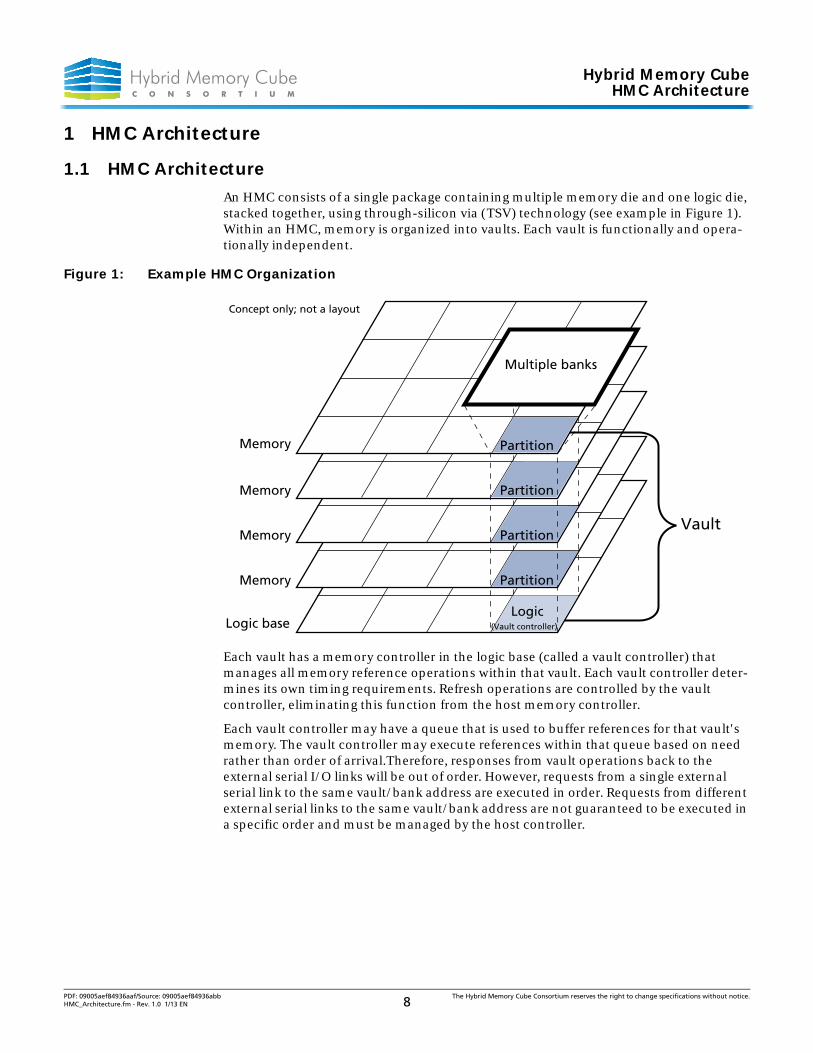
An HMC consists of a single package containing multiple memory die and one logic die, stacked together, using through-silicon via (TSV) technology (see example in Figure 1). Within an HMC, memory is organized into vaults. Each vault is functionally and opera-tionally independent.
Figure 1: Example HMC Organization
Each vault has a memory controller in the logic base (called a vault controller) that manages all memory reference operations within that vault. Each vault controller deter-mines its own timing requirements. Refresh operations are controlled by the vault controller, eliminating this function from the host memory controller.
Each vault controller may have a queue that is used to buffer references for that vault's memory. The vault controller may execute references within that queue based on need rather than order of arrival.Therefore, responses from vault operations back to the external serial I/O links will be out of order. However, requests from a single external serial link to the same vault/bank address are executed in order. Requests from different external serial links to the same vault/bank address are not guaranteed to be executed in a specific order and must be managed by the host controller.
Multiple banks
Memory
Memory
Memory
Memory
Logic base
Vault
Concept only; not a layout
Partition
Partition
Partition
Partition
(Vault controller)
Logic
PDF: 09005aef84936aaf/Source: 09005aef84936abb The Hybrid Memory Cube Consortium reserves the right to change specifications without notice.HMC_Architecture.fm - Rev. 1.0 1/13 EN 8
Hybrid Memory CubeHMC Architecture
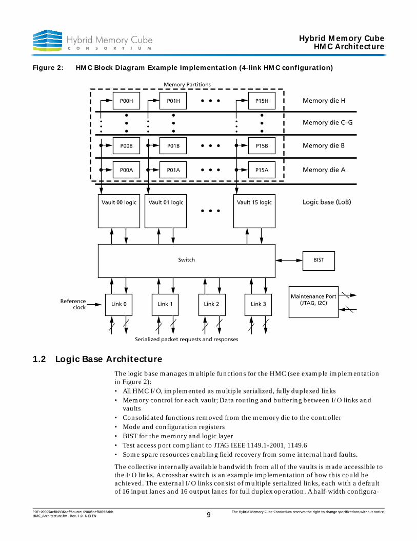
Figure 2: HMC Block Diagram Example Implementation (4-link HMC configuration)
1.2 Logic Base Architecture
The logic base manages multiple functions for the HMC (see example implementation in Figure 2):• All HMC I/O, implemented as multiple serialized, fully duplexed links• Memory control for each vault; Data routing and buffering between I/O links and
vaults• Consolidated functions removed from the memory die to the controller• Mode and configuration registers• BIST for the memory and logic layer• Test access port compliant to JTAG IEEE 1149.1-2001, 1149.6• Some spare resources enabling field recovery from some internal hard faults.
The collective internally available bandwidth from all of the vaults is made accessible to the I/O links. A crossbar switch is an example implementation of how this could be achieved. The external I/O links consist of multiple serialized links, each with a default of 16 input lanes and 16 output lanes for full duplex operation. A half-width configura-
Vault 00 logic
Link 0 Link 1 Link 2
Vault 01 logic Vault 15 logic Logic base (LoB)
BIST
Maintenance Port(JTAG, I2C)Reference
clock
Switch
Serialized packet requests and responses
Link 3
P00B
P00A
P01B
P01A
P15B
P15A
P00H P01H P15H
Memory die B
Memory die A
Memory die H
Memory die C–G
Memory Partitions
PDF: 09005aef84936aaf/Source: 09005aef84936abb The Hybrid Memory Cube Consortium reserves the right to change specifications without notice.HMC_Architecture.fm - Rev. 1.0 1/13 EN 9
Hybrid Memory CubeHMC Architecture
tion is also supported, comprised of 8 input lanes and 8 output lanes per link. Each lane direction in each link has additional power-down signals for power management. The following configurations are those supported within this specification.
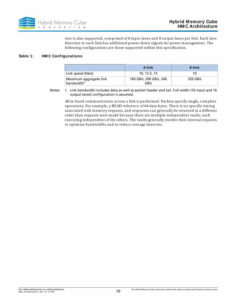
Table 1: HMC Configurations
Notes: 1. Link bandwidth includes data as well as packet header and tail. Full-width (16 input and 16 output lanes) configuration is assumed.
All in-band communication across a link is packetized. Packets specify single, complete operations. For example, a READ reference of 64 data bytes. There is no specific timing associated with memory requests, and responses can generally be returned in a different order than requests were made because there are multiple independent vaults, each executing independent of the others. The vaults generally reorder their internal requests to optimize bandwidths and to reduce average latencies.
4-link 8-link
Link speed (Gb/s) 10, 12.5, 15 10
Maximum aggregate link bandwidth1
160 GB/s, 200 GB/s, 240 GB/s
320 GB/s
PDF: 09005aef84936aaf/Source: 09005aef84936abb The Hybrid Memory Cube Consortium reserves the right to change specifications without notice.HMC_Architecture.fm - Rev. 1.0 1/13 EN 10
Hybrid Memory CubePin Descriptions
2 Pin Descriptions
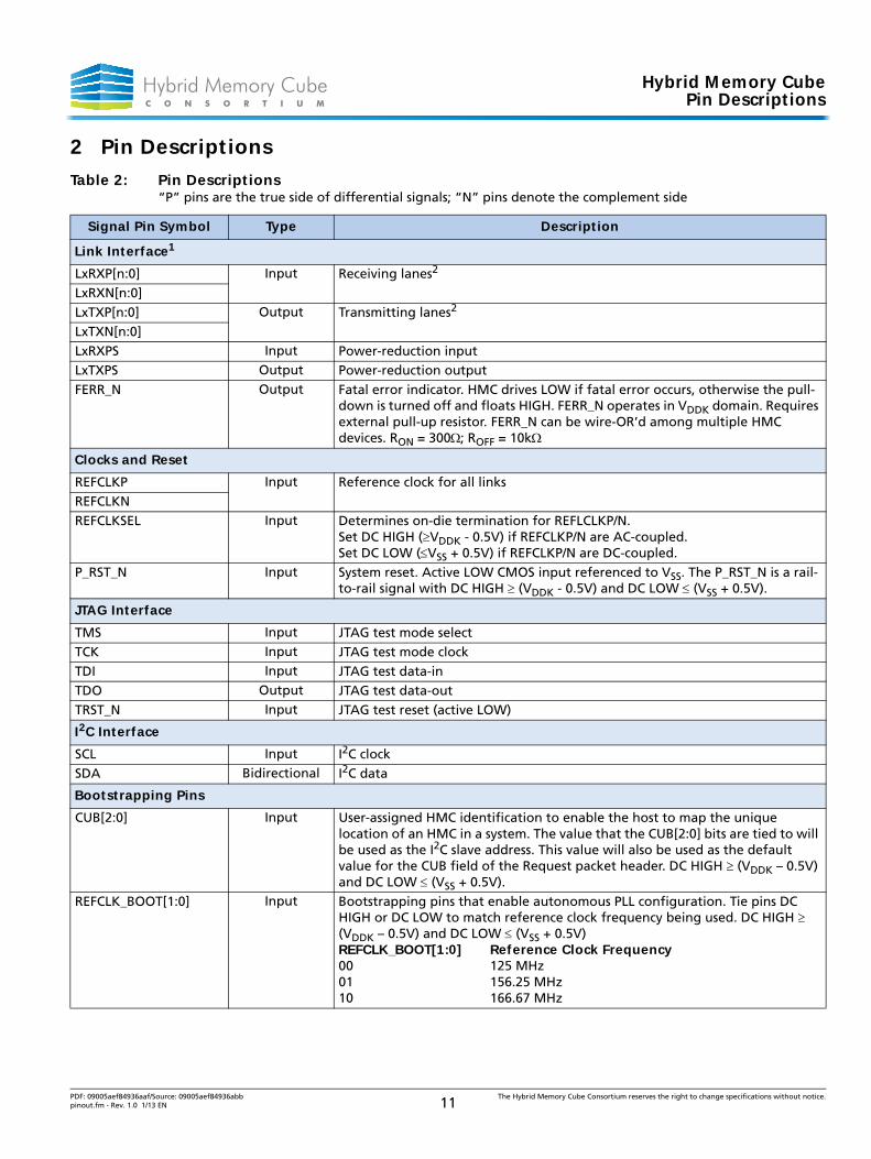
Table 2: Pin Descriptions“P” pins are the true side of differential signals; “N” pins denote the complement side
Signal Pin Symbol Type Description
Link Interface1
LxRXP[n:0] Input Receiving lanes2
LxRXN[n:0]LxTXP[n:0] Output Transmitting lanes2
LxTXN[n:0]LxRXPS Input Power-reduction inputLxTXPS Output Power-reduction outputFERR_N Output Fatal error indicator. HMC drives LOW if fatal error occurs, otherwise the pull-
down is turned off and floats HIGH. FERR_N operates in VDDK domain. Requires external pull-up resistor. FERR_N can be wire-OR’d among multiple HMC devices. RON = 300; ROFF = 10k
Clocks and Reset
REFCLKP Input Reference clock for all linksREFCLKNREFCLKSEL Input Determines on-die termination for REFLCLKP/N.
Set DC HIGH (VDDK - 0.5V) if REFCLKP/N are AC-coupled.Set DC LOW (VSS + 0.5V) if REFCLKP/N are DC-coupled.
P_RST_N Input System reset. Active LOW CMOS input referenced to VSS. The P_RST_N is a rail-to-rail signal with DC HIGH (VDDK - 0.5V) and DC LOW (VSS + 0.5V).
JTAG Interface
TMS Input JTAG test mode selectTCK Input JTAG test mode clockTDI Input JTAG test data-inTDO Output JTAG test data-outTRST_N Input JTAG test reset (active LOW)
I2C Interface
SCL Input I2C clockSDA Bidirectional I2C data
Bootstrapping Pins
CUB[2:0] Input User-assigned HMC identification to enable the host to map the unique location of an HMC in a system. The value that the CUB[2:0] bits are tied to will be used as the I2C slave address. This value will also be used as the default value for the CUB field of the Request packet header. DC HIGH (VDDK – 0.5V) and DC LOW (VSS + 0.5V).
REFCLK_BOOT[1:0] Input Bootstrapping pins that enable autonomous PLL configuration. Tie pins DC HIGH or DC LOW to match reference clock frequency being used. DC HIGH (VDDK – 0.5V) and DC LOW (VSS + 0.5V)REFCLK_BOOT[1:0] Reference Clock Frequency00 125 MHz01 156.25 MHz10 166.67 MHz
PDF: 09005aef84936aaf/Source: 09005aef84936abb The Hybrid Memory Cube Consortium reserves the right to change specifications without notice.pinout.fm - Rev. 1.0 1/13 EN 11
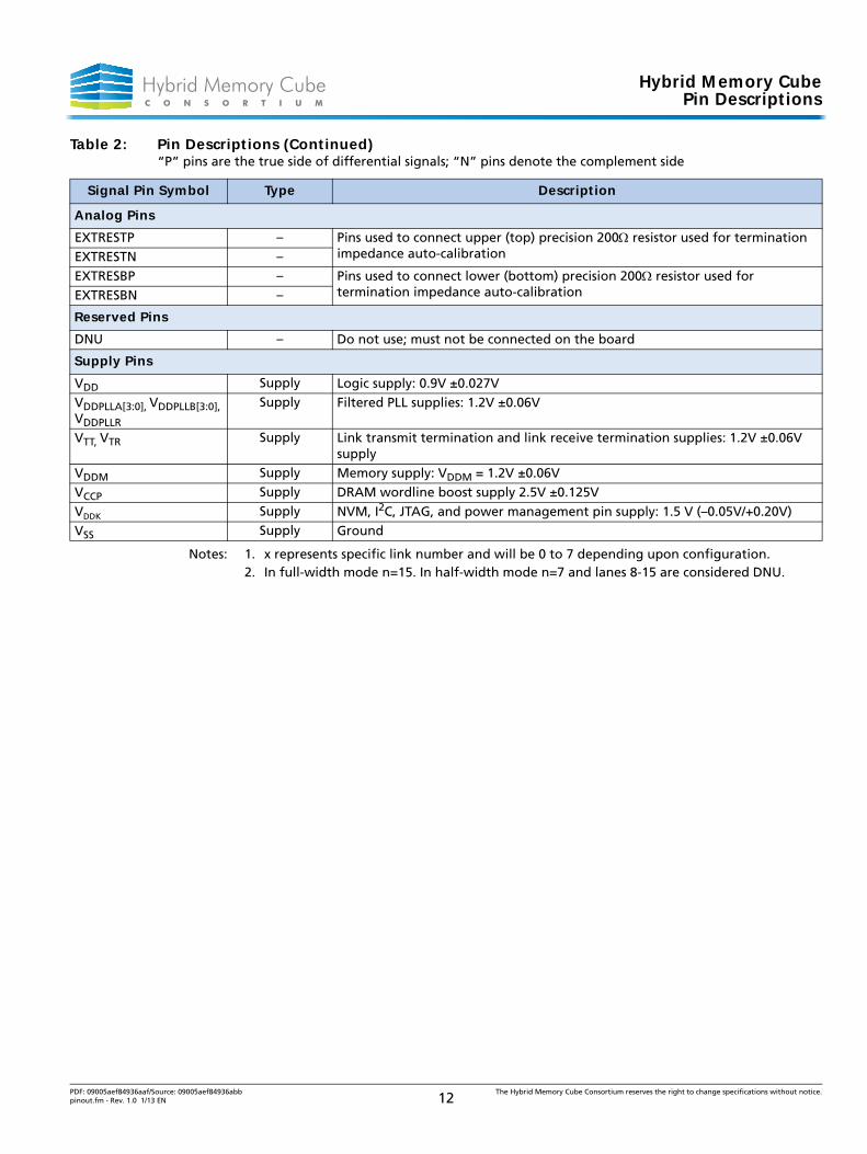
Hybrid Memory CubePin Descriptions
Notes: 1. x represents specific link number and will be 0 to 7 depending upon configuration.2. In full-width mode n=15. In half-width mode n=7 and lanes 8-15 are considered DNU.
Analog Pins
EXTRESTP – Pins used to connect upper (top) precision 200 resistor used for termination impedance auto-calibrationEXTRESTN –
EXTRESBP – Pins used to connect lower (bottom) precision 200 resistor used for termination impedance auto-calibrationEXTRESBN –
Reserved Pins
DNU – Do not use; must not be connected on the board
Supply Pins
VDD Supply Logic supply: 0.9V ±0.027VVDDPLLA[3:0], VDDPLLB[3:0], VDDPLLR
Supply Filtered PLL supplies: 1.2V ±0.06V
VTT, VTR Supply Link transmit termination and link receive termination supplies: 1.2V ±0.06V supply
VDDM Supply Memory supply: VDDM = 1.2V ±0.06VVCCP Supply DRAM wordline boost supply 2.5V ±0.125VVDDK Supply NVM, I2C, JTAG, and power management pin supply: 1.5 V (–0.05V/+0.20V)VSS Supply Ground
Table 2: Pin Descriptions (Continued)“P” pins are the true side of differential signals; “N” pins denote the complement side
Signal Pin Symbol Type Description
PDF: 09005aef84936aaf/Source: 09005aef84936abb The Hybrid Memory Cube Consortium reserves the right to change specifications without notice.pinout.fm - Rev. 1.0 1/13 EN 12
PDF: 09005aef84936aaf/Source: 09005aef84936abb The Hybrid Memory Cube Consortium reserves the right to change specifications without notice.Link_Data.fm - Rev. 1.0 1/13 EN 13
Hybrid Memory CubeLink Data Transmission
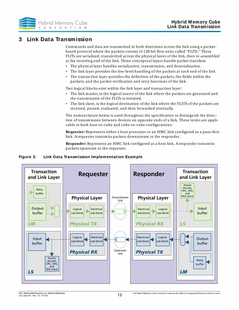
3 Link Data TransmissionCommands and data are transmitted in both directions across the link using a packet-based protocol where the packets consist of 128-bit flow units called “FLITs.” These FLITs are serialized, transmitted across the physical lanes of the link, then re-assembled at the receiving end of the link. Three conceptual layers handle packet transfers: • The physical layer handles serialization, transmission, and deserialization.• The link layer provides the low-level handling of the packets at each end of the link.• The transaction layer provides the definition of the packets, the fields within the
packets, and the packet verification and retry functions of the link.
Two logical blocks exist within the link layer and transaction layer:• The link master, is the logical source of the link where the packets are generated and
the transmission of the FLITs is initiated. • The link slave, is the logical destination of the link where the FLITS of the packets are
received, parsed, evaluated, and then forwarded internally.
The nomenclature below is used throughout the specification to distinguish the direc-tion of transmission between devices on opposite ends of a link. These terms are appli-cable to both host-to-cube and cube-to-cube configurations.
Requester: Represents either a host processor or an HMC link configured as a pass-thru link. A requester transmits packets downstream to the responder.
Responder: Represents an HMC link configured as a host link. A responder transmits packets upstream to the requester.
Figure 3: Link Data Transmission Implementation Example
Inputbuffer
Electricalsub-block
Packetdecode,
CRC, LNG,and
SEQ check
Logicalsub-block
LSPhysical RX
Physical Layer
Outputbuffer
Electricalsub-block
Retrybuffer
Logicalsub-block
LM
Physical TX
Responder Transactionand Link Layer
Outputbuffer
Logicalsub-block
Retrybuffer
Electricalsub-block
Upstreamlink
Downstreamlink
LM Physical TX
Physical Layer
Inputbuffer
Logicalsub-block
Packetdecode,
CRC, LNG,and
SEQ check
Electricalsub-block
LS
Physical RX
RequesterTransactionand Link Layer
Hybrid Memory CubeLogical Sub-Block of Physical Layer
4 Logical Sub-Block of Physical LayerThe transfer of information across the links consists of 128-bit FLITs. Each FLIT takes the following path through the serial link:1. 128-bit FLITs are generated by the link master and sent in parallel to the transmitting
logical sub-block in the physical layer.2. The transmitting logical sub-block serializes each FLIT and drives it across the link
interface in a bit-serial form on each of the lanes.3. The receiving logical sub-block deserializes each lane and recreates the 128-bit paral-
lel FLIT. Receive deserializer FLIT alignment is achieved during link initialization.4. The 128-bit parallel FLIT is sent to the link layer link slave section.
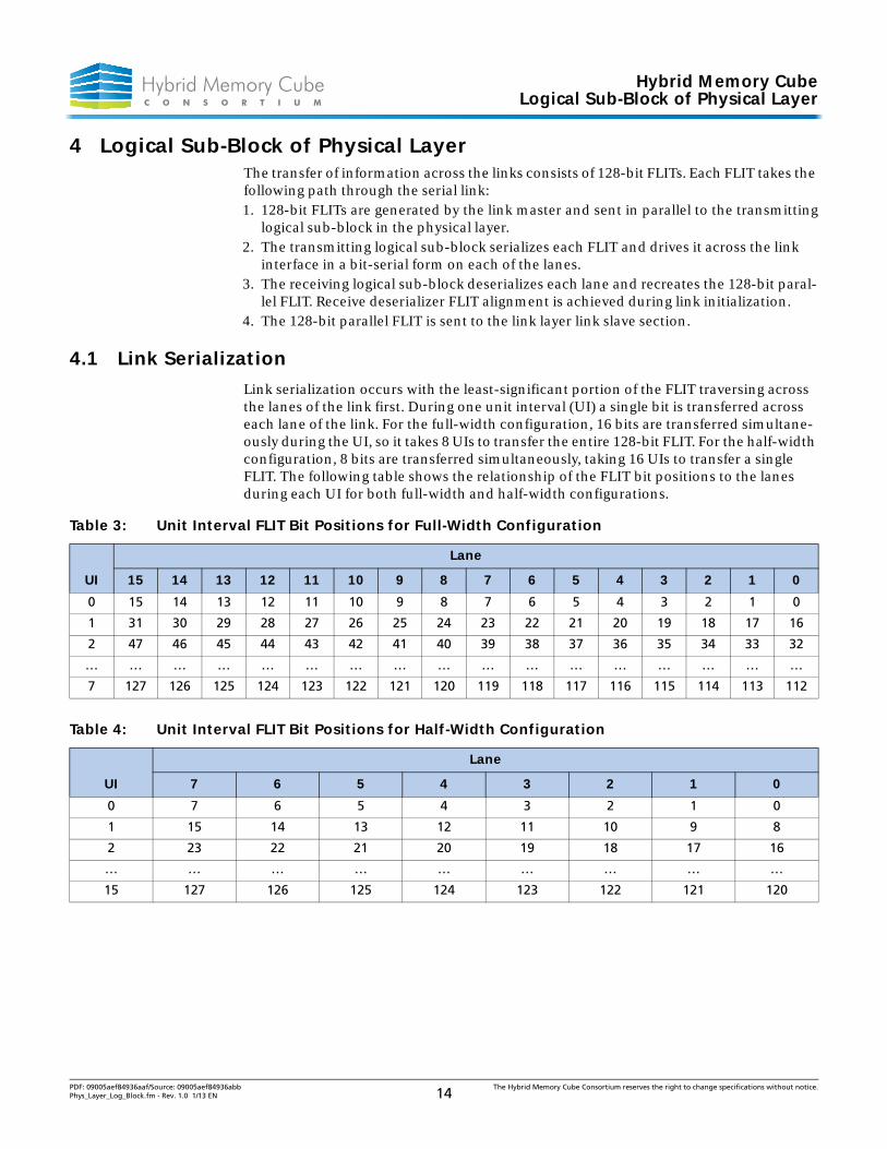
4.1 Link Serialization
Link serialization occurs with the least-significant portion of the FLIT traversing across the lanes of the link first. During one unit interval (UI) a single bit is transferred across each lane of the link. For the full-width configuration, 16 bits are transferred simultane-ously during the UI, so it takes 8 UIs to transfer the entire 128-bit FLIT. For the half-width configuration, 8 bits are transferred simultaneously, taking 16 UIs to transfer a single FLIT. The following table shows the relationship of the FLIT bit positions to the lanes during each UI for both full-width and half-width configurations.
Table 3: Unit Interval FLIT Bit Positions for Full-Width Configuration
UI
Lane
15 14 13 12 11 10 9 8 7 6 5 4 3 2 1 0
0 15 14 13 12 11 10 9 8 7 6 5 4 3 2 1 0
1 31 30 29 28 27 26 25 24 23 22 21 20 19 18 17 16
2 47 46 45 44 43 42 41 40 39 38 37 36 35 34 33 32
… … … … … … … … … … … … … … … … …
7 127 126 125 124 123 122 121 120 119 118 117 116 115 114 113 112
Table 4: Unit Interval FLIT Bit Positions for Half-Width Configuration
UI
Lane
7 6 5 4 3 2 1 0
0 7 6 5 4 3 2 1 0
1 15 14 13 12 11 10 9 8
2 23 22 21 20 19 18 17 16
… … … … … … … … …
15 127 126 125 124 123 122 121 120
PDF: 09005aef84936aaf/Source: 09005aef84936abb The Hybrid Memory Cube Consortium reserves the right to change specifications without notice.Phys_Layer_Log_Block.fm - Rev. 1.0 1/13 EN 14
Hybrid Memory CubeLogical Sub-Block of Physical Layer
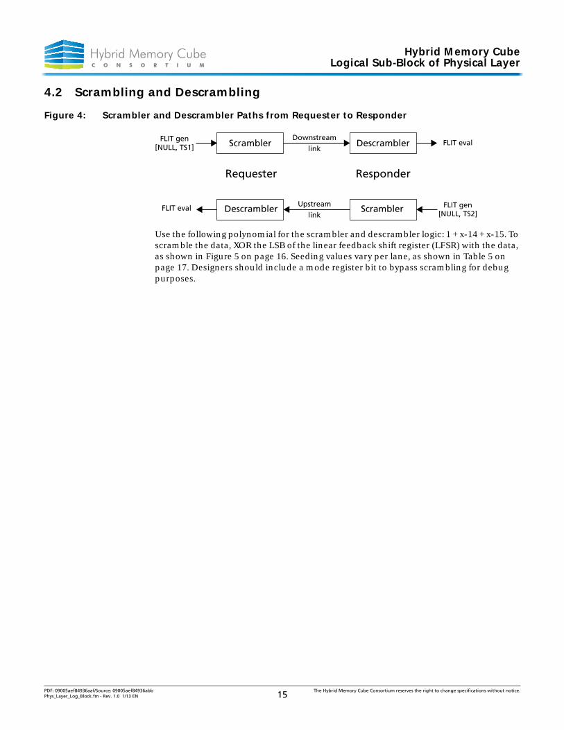
4.2 Scrambling and Descrambling
Figure 4: Scrambler and Descrambler Paths from Requester to Responder
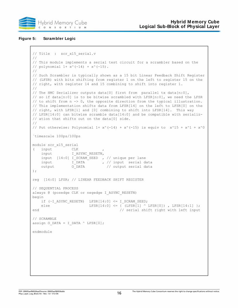
Use the following polynomial for the scrambler and descrambler logic: 1 + x-14 + x-15. To scramble the data, XOR the LSB of the linear feedback shift register (LFSR) with the data, as shown in Figure 5 on page 16. Seeding values vary per lane, as shown in Table 5 on page 17. Designers should include a mode register bit to bypass scrambling for debug purposes.
Scrambler Descrambler
Descrambler
Requester Responder
FLIT gen[NULL, TS1]
Downstream
link
Upstream
linkFLIT gen
[NULL, TS2]
FLIT eval
FLIT eval Scrambler
PDF: 09005aef84936aaf/Source: 09005aef84936abb The Hybrid Memory Cube Consortium reserves the right to change specifications without notice.Phys_Layer_Log_Block.fm - Rev. 1.0 1/13 EN 15
Hybrid Memory CubeLogical Sub-Block of Physical Layer
Figure 5: Scrambler Logic
// Title : scr_x15_serial.v//// This module implements a serial test circuit for a scrambler based on the// polynomial 1+ x^(-14) + x^(-15). //// Such Scrambler is typically shown as a 15 bit Linear Feedback Shift Register// (LFSR) with bits shifting from register 1 on the left to register 15 on the // right, with register 14 and 15 combining to shift into register 1. // // The HMC Serializer outputs data[0] first from parallel tx data[n:0], // so if data[n:0] is to be bitwise scrambled with LFSR[n:0], we need the LFSR // to shift from n -> 0, the opposite direction from the typical illustration. // This implementation shifts data from LFSR[14] on the left to LFSR[0] on the // right, with LFSR[1] and [0] combining to shift into LFSR[14]. This way // LFSR[14:0] can bitwise scramble data[14:0] and be compatible with serializ-// ation that shifts out on the data[0] side.//// Put otherwise: Polynomial 1+ x^(-14) + x^(-15) is equiv to x^15 + x^1 + x^0
`timescale 100ps/100ps
module scr_x15_serial ( input CLK , input I_ASYNC_RESETN, input [14:0] I_SCRAM_SEED , // unique per lane input I_DATA , // input serial data output O_DATA // output serial data);
reg [14:0] LFSR; // LINEAR FEEDBACK SHIFT REGISTER
// SEQUENTIAL PROCESS always @ (posedge CLK or negedge I_ASYNC_RESETN)begin if (~I_ASYNC_RESETN) LFSR[14:0] <= I_SCRAM_SEED; else LFSR[14:0] <= { (LFSR[1] ^ LFSR[0]) , LFSR[14:1] };end // serial shift right with left input
// SCRAMBLEassign O_DATA = I_DATA ^ LFSR[0];
endmodule
PDF: 09005aef84936aaf/Source: 09005aef84936abb The Hybrid Memory Cube Consortium reserves the right to change specifications without notice.Phys_Layer_Log_Block.fm - Rev. 1.0 1/13 EN 16
Hybrid Memory CubeLogical Sub-Block of Physical Layer
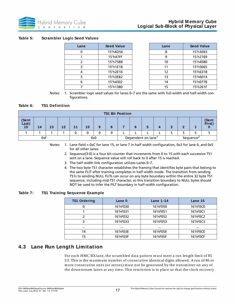
Notes: 1. Scrambler logic seed values for lanes 0–7 are the same with full-width and half-width con-figurations.
Notes: 1. Lane field = 0xC for lane 15, or lane 7 in half width configuration, 0x3 for lane 0, and 0x5 for all other lanes.
2. Sequence[3:0] is a four bit counter that increments from 0 to 15 with each successive TS1 sent on a lane. Sequence value will roll back to 0 after 15 is reached.
3. The half width link configuration utilizes Lanes 0–7.4. The two byte TS1 character establishes the framing that identifies byte pairs that belong to
the same FLIT after training completes in half-width mode. The transition from sending TS1s to sending NULL FLITs can occur on any byte boundary within the entire 32 byte TS1 sequence, including mid-TS1 character, so this transition boundary to NULL bytes should NOT be used to infer the FILT boundary in half-width configuration.
4.3 Lane Run Length Limitation
For each HMC RX lane, the scrambled data pattern must meet a run length limit of 85 UI. This is the maximum number of consecutive identical digits allowed. A run of 86 or more consecutive ones (or zeroes) must not be generated by the transmitter on any of the downstream lanes at any time. This restriction is in place so that the clock recovery
Table 5: Scrambler Logic Seed Values
Lane Seed Value Lane Seed Value
0 15’h4D56 8 15’h3EB31 15’h47FF 9 15’h27692 15’h75B8 10 15’h45803 15’h1E18 11 15’h56654 15’h2E10 12 15’h63185 15’h3EB2 13 15’h60146 15’h4302 14 15’h077B7 15’h1380 15 15’h261F
Table 6: TS1 Definition
TS1 Bit Position
(Sent Last)
15 14 13 12 11 10 9 8 7 6 5 4 3 2 1
(Sent First)
0
1 1 1 1 0 0 0 0 L L L L S S S S0xF 0x0 Dependent on lane1 Sequence2
Table 7: TS1 Training Sequence Example
TS1 Ordering Lane 0 Lane 1–14 Lane 15
0 16'hF030 16'hF050 16'hF0C01 16'hF031 16'hF051 16'hF0C12 16'hF032 16'hF052 16'hF0C23 16'hF033 16'hF053 16'hF0C3... ... ... ...14 16'hF03E 16'hF05E 16'hF0CE15 16'hF03F 16'hF05F 16'hF0CF
PDF: 09005aef84936aaf/Source: 09005aef84936abb The Hybrid Memory Cube Consortium reserves the right to change specifications without notice.Phys_Layer_Log_Block.fm - Rev. 1.0 1/13 EN 17
Hybrid Memory CubeLogical Sub-Block of Physical Layer
circuit at each HMC RX lane meets its minimum required transition density to assure correct data alignment. This restriction does not require a particular implementation of the transmitter logic, as long as the run length limit is met at the HMC RX lane inputs.
Although a given host may not have a run length limit on the scrambled upstream data, the HMC is designed to meet run length limitations of 85 UI on each lane at all times. This is implemented through the HMC’s ability to monitor the scrambled data at each TX lane. If the scrambled TX data on any lane exceeds 85 consecutive digits, the TX scramble logic forces at least one transition. Forcing a transition corrupts the upstream response and results in a link retry (see 11 “Link Retry” on page 61). The probability of such an event is approximately 2-80 for random payload data. The HMC run length limi-tation feature may be disabled within the mode register.
4.4 Lane Reversal
In order to accommodate different external link routing topologies, the RX logical sub-block has the capability to reverse the lane bit number assignment. Lane reversal at the HMC is detected during initialization when receiving the TS1 training sequence and is automatically compensated for by logic in each receiving logical sub-block that reas-signs external Lane 0 to connect to Lane 15 internally, Lane 1 to connect to Lane 14 inter-nally, and so on. Once lane ordering is detected and set by the HMC logical sub-block, it remains unchanged thereafter. The lane reversal mode does not have to be the same for both directions of the link. An HMC component may have one or more links with lane reversal enabled at their respective receivers. The host is responsible for any implemen-tation of lane reversal from the upstream lanes.
4.5 Lane Polarity
In order to accommodate different external Link routing topologies, the RX logical sub-block has the capability to logically invert the received data on a lane-by-lane basis. The polarity is determined during link initialization and remains unchanged thereafter. The training sequence is used to infer polarity at the HMC receiver. The requester is respon-sible for any implementation of lane polarity inversion from upstream lanes.
PDF: 09005aef84936aaf/Source: 09005aef84936abb The Hybrid Memory Cube Consortium reserves the right to change specifications without notice.Phys_Layer_Log_Block.fm - Rev. 1.0 1/13 EN 18
Hybrid Memory CubeChaining
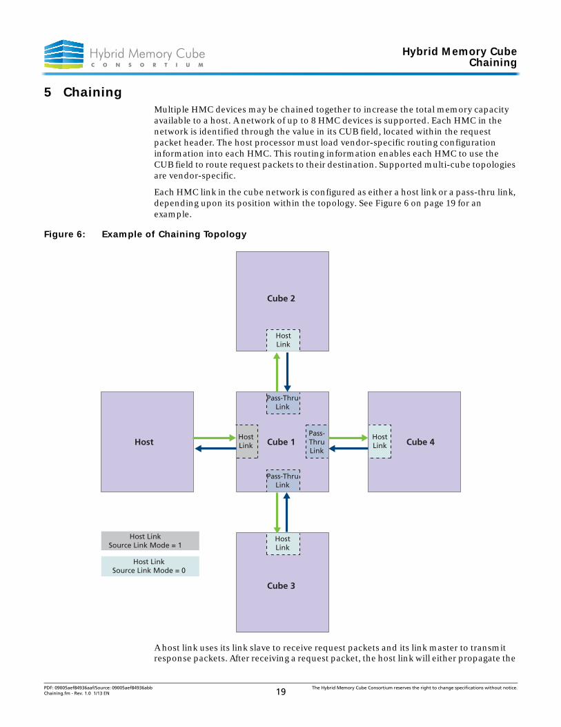
5 ChainingMultiple HMC devices may be chained together to increase the total memory capacity available to a host. A network of up to 8 HMC devices is supported. Each HMC in the network is identified through the value in its CUB field, located within the request packet header. The host processor must load vendor-specific routing configuration information into each HMC. This routing information enables each HMC to use the CUB field to route request packets to their destination. Supported multi-cube topologies are vendor-specific.
Each HMC link in the cube network is configured as either a host link or a pass-thru link, depending upon its position within the topology. See Figure 6 on page 19 for an example.
Figure 6: Example of Chaining Topology
A host link uses its link slave to receive request packets and its link master to transmit response packets. After receiving a request packet, the host link will either propagate the
Cube 1 Cube 4
Cube 3
Host
Cube 2
HostLink
Host LinkSource Link Mode = 1
Host LinkSource Link Mode = 0
Pass-ThruLink
Pass-ThruLink
Pass-ThruLink
HostLink
HostLink
HostLink
PDF: 09005aef84936aaf/Source: 09005aef84936abb The Hybrid Memory Cube Consortium reserves the right to change specifications without notice.Chaining.fm - Rev. 1.0 1/13 EN 19
Hybrid Memory CubeChaining
packet to its own internal vault destination (if the value in the CUB field matches its pro-grammed cube ID) or forward it towards its destination in another HMC via a link con-figured as a pass-thru link.
A pass-thru link uses its link master to transmit the request packet towards its destina-tion cube, and its link slave to receive response packets destined for the host processor.
The HMC link connected directly to the host processor must be configured as a host link in source mode. The link slave of the host link in source mode has the responsibility to generate and insert a unique value into the source link identifier (SLID) field within the tail of each request packet. The unique SLID value is used to identify the source link for response routing. The SLID value does not serve any function within the request packet other than to traverse the cube network to its destination vault where it is then inserted into the header of the corresponding response packet. The host processor must load vendor-specific routing configuration information into each HMC. This routing infor-mation enables each HMC to use the SLID value to route response packets to their desti-nation. Only a host link in source mode will generate a SLID for each request packet. On the opposite side of a pass-thru link is a host link that is NOT in source mode. This host link operates with the same characteristics as the host link in source mode except that it does not generate and insert a new value into the SLID field within a request packet. All link slaves in pass-thru mode use the SLID value generated by the host link in source mode for response routing purposes only. The SLID fields within the request packet tail and the response packet header are considered ‘Don’t Care’ by the host processor.
PDF: 09005aef84936aaf/Source: 09005aef84936abb The Hybrid Memory Cube Consortium reserves the right to change specifications without notice.Chaining.fm - Rev. 1.0 1/13 EN 20
Hybrid Memory CubePower-On and Initialization
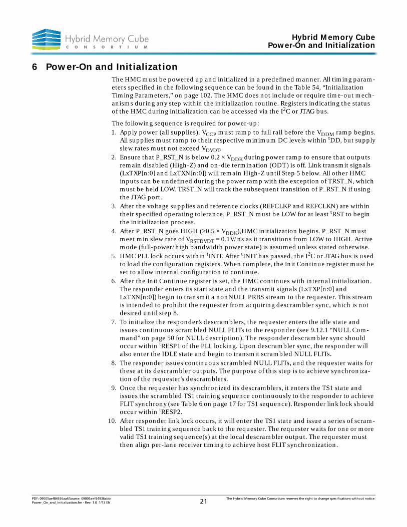
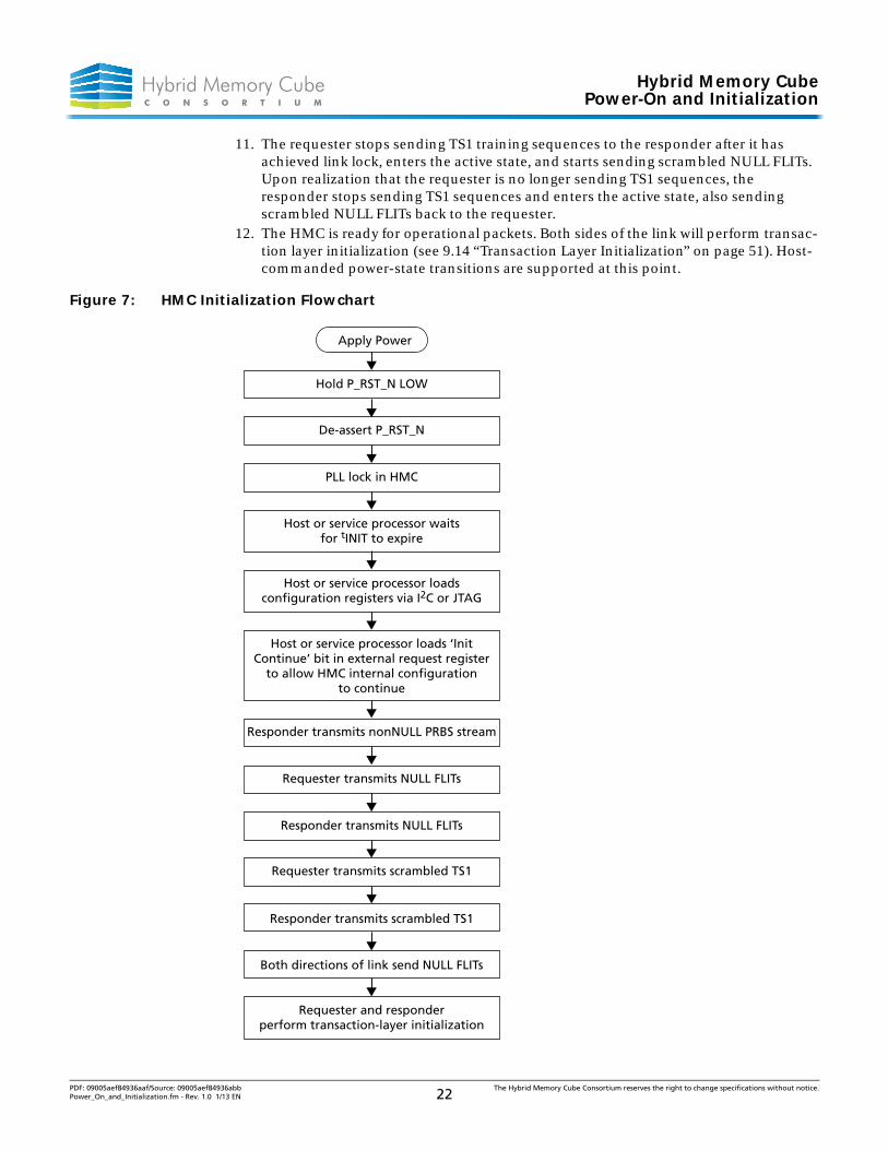
6 Power-On and InitializationThe HMC must be powered up and initialized in a predefined manner. All timing param-eters specified in the following sequence can be found in the Table 54, “Initialization Timing Parameters,” on page 102. The HMC does not include or require time-out mech-anisms during any step within the initialization routine. Registers indicating the status of the HMC during initialization can be accessed via the I2C or JTAG bus.
The following sequence is required for power-up:1. Apply power (all supplies). VCCP must ramp to full rail before the VDDM ramp begins.
All supplies must ramp to their respective minimum DC levels within tDD, but supplyslew rates must not exceed VDVDT.
2. Ensure that P_RST_N is below 0.2 × VDDK during power ramp to ensure that outputs remain disabled (High-Z) and on-die termination (ODT) is off. Link transmit signals (LxTXP[n:0] and LxTXN[n:0]) will remain High-Z until Step 5 below. All other HMC inputs can be undefined during the power ramp with the exception of TRST_N, which must be held LOW. TRST_N will track the subsequent transition of P_RST_N if using the JTAG port.
3. After the voltage supplies and reference clocks (REFCLKP and REFCLKN) are within their specified operating tolerance, P_RST_N must be LOW for at least tRST to begin the initialization process.
4. After P_RST_N goes HIGH (0.5 × VDDK),HMC initialization begins. P_RST_N must meet min slew rate of VRSTDVDT = 0.1V/ns as it transitions from LOW to HIGH. Active mode (full-power/high bandwidth power state) is assumed unless stated otherwise.
5. HMC PLL lock occurs within tINIT. After tINIT has passed, the I2C or JTAG bus is used to load the configuration registers. When complete, the Init Continue register must be set to allow internal configuration to continue.
6. After the Init Continue register is set, the HMC continues with internal initialization. The responder enters its start state and the transmit signals (LxTXP[n:0] and LxTXN[n:0]) begin to transmit a nonNULL PRBS stream to the requester. This stream is intended to prohibit the requester from acquiring descrambler sync, which is not desired until step 8.
7. To initialize the responder’s descramblers, the requester enters the idle state and issues continuous scrambled NULL FLITs to the responder (see 9.12.1 “NULL Com-mand” on page 50 for NULL description). The responder descrambler sync should occur within tRESP1 of the PLL locking. Upon descrambler sync, the responder will also enter the IDLE state and begin to transmit scrambled NULL FLITs.
8. The responder issues continuous scrambled NULL FLITs, and the requester waits for these at its descrambler outputs. The purpose of this step is to achieve synchroniza-tion of the requester’s descramblers.
9. Once the requester has synchronized its descramblers, it enters the TS1 state and issues the scrambled TS1 training sequence continuously to the responder to achieve FLIT synchrony (see Table 6 on page 17 for TS1 sequence). Responder link lock should occur within tRESP2.
10. After responder link lock occurs, it will enter the TS1 state and issue a series of scram-bled TS1 training sequence back to the requester. The requester waits for one or more valid TS1 training sequence(s) at the local descrambler output. The requester must then align per-lane receiver timing to achieve host FLIT synchronization.
PDF: 09005aef84936aaf/Source: 09005aef84936abb The Hybrid Memory Cube Consortium reserves the right to change specifications without notice.Power_On_and_Initialization.fm - Rev. 1.0 1/13 EN 21
Hybrid Memory CubePower-On and Initialization
11. The requester stops sending TS1 training sequences to the responder after it has achieved link lock, enters the active state, and starts sending scrambled NULL FLITs. Upon realization that the requester is no longer sending TS1 sequences, the responder stops sending TS1 sequences and enters the active state, also sending scrambled NULL FLITs back to the requester.
12. The HMC is ready for operational packets. Both sides of the link will perform transac-tion layer initialization (see 9.14 “Transaction Layer Initialization” on page 51). Host-commanded power-state transitions are supported at this point.
Figure 7: HMC Initialization Flowchart
Apply Power
Hold P_RST_N LOW
De-assert P_RST_N
PLL lock in HMC
Host or service processor waitsfor tINIT to expire
Host or service processor loadsconfiguration registers via I2C or JTAG
Host or service processor loads ‘InitContinue’ bit in external request register
to allow HMC internal configurationto continue
Responder transmits nonNULL PRBS stream
Requester transmits NULL FLITs
Responder transmits NULL FLITs
Requester transmits scrambled TS1
Responder transmits scrambled TS1
Both directions of link send NULL FLITs
Requester and responderperform transaction-layer initialization
PDF: 09005aef84936aaf/Source: 09005aef84936abb The Hybrid Memory Cube Consortium reserves the right to change specifications without notice.Power_On_and_Initialization.fm - Rev. 1.0 1/13 EN 22
Hybrid Memory CubePower-On and Initialization
Figure 8: Initialization Timing
Notes: 1. Data on links is scrambled.
Supply voltages
Downstream link(toward responder)
REFCLKP
P_RST_N
Upstream link(toward requester)
tDD
tRST
tRESP1
tINIT
I2C or JTAGbus
tRESP2
High-Z
NULL
Configuration Register Load
TS1 NULL
TS1 NULL
TRET Packets
TRET PacketsNULLPRBS
PDF: 09005aef84936aaf/Source: 09005aef84936abb The Hybrid Memory Cube Consortium reserves the right to change specifications without notice.Power_On_and_Initialization.fm - Rev. 1.0 1/13 EN 23

Hybrid Memory CubePower State Management
7 Power State ManagementEach link can independently be set into a lower power state through the usage of the power state management pins, LxRXPS and LxTXPS. Each of the links can be set into a low-power state, sleep mode, as well as a minimum power state called down mode.
Power is reduced when sleep mode is entered from normal operation (active mode) through the disablement of the link’s high-speed SerDes circuitry. After a link has been initialized and is in active mode, the requester can transition its power state manage-ment pin, LxTXPS, from HIGH to LOW to put the opposite side of the link (responder) into sleep mode. As it begins to enter sleep mode, the responder will transition it’s LxTXPS from HIGH to LOW within the tPST specified timing. Values for tPST and all other power state management related timing can be found in Table 55, “Link Power Management Parameters,” on page 103. Transition of the responder’s LxTXPS will initiate the requester’s Rx and Tx lanes to enter into sleep mode as well. It is the responsi-bility of the host to quiesce traffic (ensure closure on all in-flight transactions) prior to exiting active mode link state. The responder’s link logic is not responsible for in-flight transactions when LxRXPS goes from 1 to 0.
Down mode allows a link to go to an even lower power state than sleep mode by disabling both the high-speed SerDes circuitry as well as the link’s PLLs. A link enters down mode if its corresponding LxRXPS signal is LOW when the P_RST_N signal transi-tions from LOW to HIGH either during initialization or a reset event. The HMC can be configured so that all of its links will enter down mode after the last link in active mode transitions to sleep mode. In this setting, any link already in sleep mode when the last link exits active mode will be transitioned to down mode to further reduce power consumption. Transitioning any links from sleep mode to down mode will take up to 150µs (represented by tSD specification).
When all links exit active mode and transition to down mode, the HMC enters a self refresh state. Although not accessible from the links, data stored within the memory is still maintained . Upon entering self refresh the HMC must stay in this state for a minimum of 1ms (tSREF). This is measured from the time the HMC’s last link transitions its LxRXPS LOW (entering self refresh) to its first LxRXPS to transition HIGH (entering active mode).
All links will independently respond to power state control; however, in the event of simultaneous power state transitions, the HMC will stagger transitions between active mode and sleep modes in order to avoid supply voltage shifts. The amount of stagger time incurred is defined by the tSS specification. Multiply tSS by n - 1 to determine when the final link will transition states, where n equals the number of simultaneous link tran-sitions. For example, if the requester sets its L0TXPS, L1TXPS, L2TXPS, and L3TXPS to 0 at the same time, it will take 1.5µs for the HMC to transition all four links into sleep mode (tSS × 3). This is also true for links exiting sleep mode and entering active mode. As an example, if L0RXPS and L1RXPS transition from LOW to HIGH at the same time, the second links will not start the transition to active mode until up to 500ns later (tSS × 1).
The transition of a link to active mode from either sleep mode or down mode requires a re-initialization sequence as illustrated in Figure 9.
Bringing a link up from down mode into active mode requires additional time to complete the HSS PLL self-calibration as is specified by tPSC (see Note 3 of Figure 9).
PDF: 09005aef84936aaf/Source: 09005aef84936abb The Hybrid Memory Cube Consortium reserves the right to change specifications without notice.power_state_management.fm - Rev. 1.0 1/13 EN 24
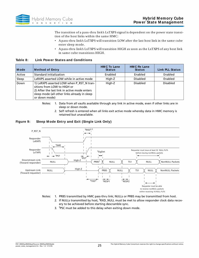
Hybrid Memory CubePower State Management
The transition of a pass-thru link’s LxTXPS signal is dependent on the power state transi-tion of the host links within the same HMC: • A pass-thru link’s LxTXPS will transition LOW after the last host link in the same cube
enter sleep mode.• A pass-thru link’s LxTXPS will transition HIGH as soon as the LxTXPS of any host link
in same cube transitions HIGH.
Notes: 1. Data from all vaults available through any link in active mode, even if other links are in sleep or down mode.
2. Self refresh is entered when all links exit active mode whereby data in HMC memory is retained but unavailable.
Figure 9: Sleep Mode Entry and Exit (Single Link Only)
Notes: 1. PRBS transmitted by HMC pass-thru link; NULLs or PRBS may be transmitted from host.2. If NULLs transmitted by host, tRXD_NULL must be met to allow responder clock data recov-
ery to be achieved before starting descramble sync.3. tPSC must be added to this delay when exiting down mode.
Table 8: Link Power States and Conditions
Mode Method of EntryHMC Tx Lane
StatusHMC Rx Lane
Status Link PLL Status
Active Standard initialization Enabled Enabled Enabled
Sleep LxRXPS asserted LOW while in active mode High-Z Disabled Enabled
Down 1) LxRXPS asserted LOW when P_RST_N tran-sitions from LOW to HIGH or2) After the last link in active mode enters sleep mode (all other links already in sleep or down mode)
High-Z Disabled Disabled
ResponderLxRXPS
P_RST_N
ResponderLxTXPS
NULL PRBS
PRBS1
NULL
NULL
NULL NonNULL Packets
NonNULL PacketsTS1
TS1High-Z
tPST
tSME
Upstream Link(Toward requester)
NULL NULLHigh-ZDownstream Link
(Toward responder)
tPST
tSigDet
tRESP1tTXD3
tRXD2,3
tRESP2
Requester must issue at least 32 NULL FLITs
before issuing nonNULL packets
Requester must be able
to receive nonNULL packets
within receiving 16 NULL FLITs
PDF: 09005aef84936aaf/Source: 09005aef84936abb The Hybrid Memory Cube Consortium reserves the right to change specifications without notice.power_state_management.fm - Rev. 1.0 1/13 EN 25
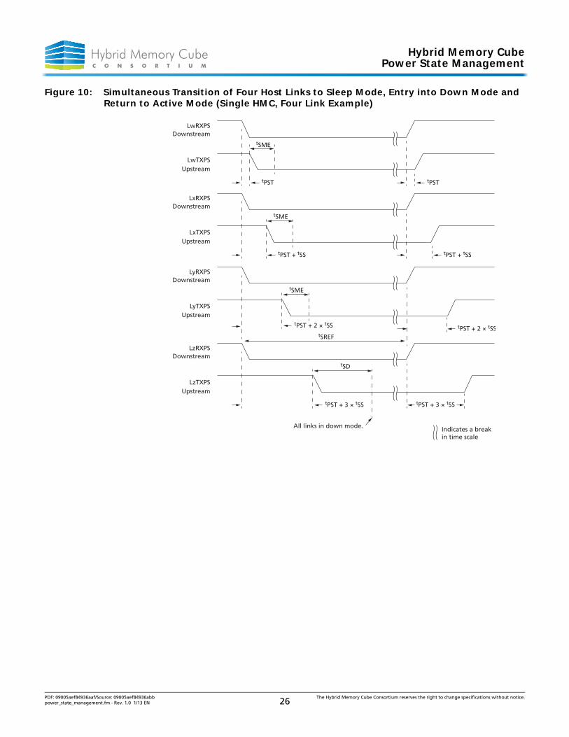
Hybrid Memory CubePower State Management
Figure 10: Simultaneous Transition of Four Host Links to Sleep Mode, Entry into Down Mode and Return to Active Mode (Single HMC, Four Link Example)
tPST
tSME
tPST
LwRXPS
LwTXPS
Downstream
Upstream
tPST + tSS
tSME
tSME
tSREF
LxRXPS
LxTXPS
Downstream
Upstream
tPST + 2 × tSS tPST + 2 × tSS
Indicates a break in time scale
LyRXPS
LyTXPS
Downstream
Upstream
tPST + tSS
tSD
tPST + 3 × tSS
All links in down mode.
tPST + 3 × tSS
LzRXPS
LzTXPS
Downstream
Upstream
PDF: 09005aef84936aaf/Source: 09005aef84936abb The Hybrid Memory Cube Consortium reserves the right to change specifications without notice.power_state_management.fm - Rev. 1.0 1/13 EN 26
PDF: 09005aef84936aaf/Source: 09005aef84936abb The Hybrid Memory Cube Consortium reserves the right to change specifications without notice.Link_Layer.fm - Rev. 1.0 1/13 EN 27
Hybrid Memory CubeLink Layer
8 Link LayerThe link layer handles communication across the link not associated with the transac-tion layer. This consists of the transmission of NULL FLITs and flow packets.
All FLITs of a packet must be transmitted sequentially, without interruption, across the link. NULL FLITs are generated at the link layer when no other packets are being transmitted. A NULL FLIT is an all-zeros pattern that is scrambled prior to transmission. Any number of packets can be streamed back-to-back across the link, or they can be separated by NULL FLITs, depending upon system traffic and transaction layer flow control. There is no minimum or maximum requirement associated with the number of NULL FLITs transmitted between packets. NULL FLITs are not subject to flow control. The first nonzero FLIT following a NULL FLIT is considered to be the first FLIT of a packet. Note that data FLITs within a packet may be all zeros, but these lie between a header FLIT and a tail FLIT.
Flow packets are generated by the link master to pass flow control and retry control commands to the opposite side of the link. Flow packets are sent when no other link traffic is occurring or when a link retry sequence is to be initiated. Flow packets are single-FLIT packets with no data payload and are not subject to flow control. Flow packets utilize the same header and tail format as request packets, but are not consid-ered requests, and do not have corresponding response commands. See Section 8.12, “Flow Commands” for specifics on the commands transmitted with flow packets.
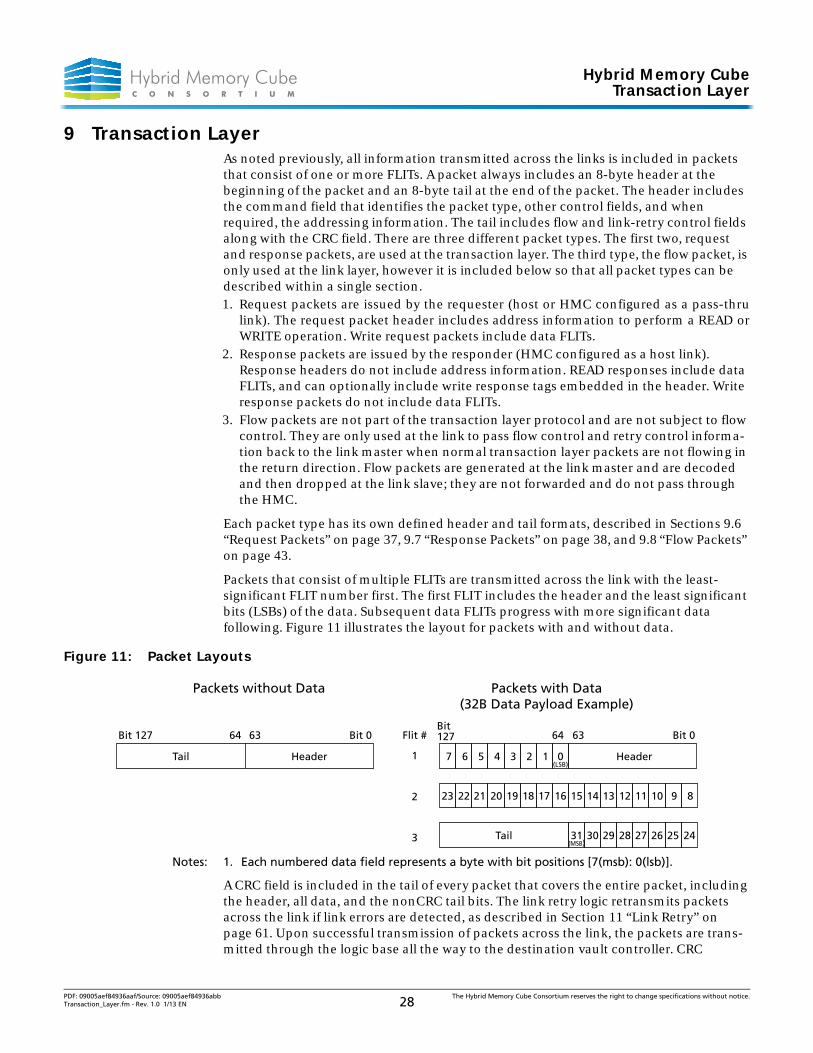
Hybrid Memory CubeTransaction Layer
9 Transaction LayerAs noted previously, all information transmitted across the links is included in packets that consist of one or more FLITs. A packet always includes an 8-byte header at the beginning of the packet and an 8-byte tail at the end of the packet. The header includes the command field that identifies the packet type, other control fields, and when required, the addressing information. The tail includes flow and link-retry control fields along with the CRC field. There are three different packet types. The first two, request and response packets, are used at the transaction layer. The third type, the flow packet, is only used at the link layer, however it is included below so that all packet types can be described within a single section.1. Request packets are issued by the requester (host or HMC configured as a pass-thru
link). The request packet header includes address information to perform a READ orWRITE operation. Write request packets include data FLITs.
2. Response packets are issued by the responder (HMC configured as a host link). Response headers do not include address information. READ responses include data FLITs, and can optionally include write response tags embedded in the header. Write response packets do not include data FLITs.
3. Flow packets are not part of the transaction layer protocol and are not subject to flow control. They are only used at the link to pass flow control and retry control informa-tion back to the link master when normal transaction layer packets are not flowing in the return direction. Flow packets are generated at the link master and are decoded and then dropped at the link slave; they are not forwarded and do not pass through the HMC.
Each packet type has its own defined header and tail formats, described in Sections 9.6 “Request Packets” on page 37, 9.7 “Response Packets” on page 38, and 9.8 “Flow Packets” on page 43.
Packets that consist of multiple FLITs are transmitted across the link with the least-significant FLIT number first. The first FLIT includes the header and the least significant bits (LSBs) of the data. Subsequent data FLITs progress with more significant data following. Figure 11 illustrates the layout for packets with and without data.
Figure 11: Packet Layouts
Notes: 1. Each numbered data field represents a byte with bit positions [7(msb): 0(lsb)].
A CRC field is included in the tail of every packet that covers the entire packet, including the header, all data, and the nonCRC tail bits. The link retry logic retransmits packets across the link if link errors are detected, as described in Section 11 “Link Retry” on page 61. Upon successful transmission of packets across the link, the packets are trans-mitted through the logic base all the way to the destination vault controller. CRC
Packets without Data Packets with Data(32B Data Payload Example)
Tail Header
Bit 127 Bit 06364
7 Header
Tail
Bit127 Bit 06364Flit #
1
2
3
6 5 4 3 2 1 0(LSB)
23 22 21 20 19 18 17 16 15 14 13 12 11 10 9 8
31(MSB)
30 29 28 27 26 25 24
PDF: 09005aef84936aaf/Source: 09005aef84936abb The Hybrid Memory Cube Consortium reserves the right to change specifications without notice.Transaction_Layer.fm - Rev. 1.0 1/13 EN 28
Hybrid Memory CubeTransaction Layer
provides command and data through-checking to the destination vault controller. ECC provides error coverage of the data from the vault controller to and from the DRAM arrays. Thus, data is protected along the entire path to and from the memory device. If the vault controller detects a correctable error, error correction is executed before the data is returned. If an uncorrectable error is detected, an error status is returned in the response packet back to the requester.
The CRC algorithm used on the HMC is the Koopman CRC-32K. This algorithm was chosen for the HMC because of its balance of coverage and ease of implementation. The polynomial for this algorithm is:
x32 + x30 + x29 + x28 + x26 + x20 + x19 + x17 + x16 + x15 + x11 + x10 + x7 + x6 + x4 + x2 + x + 1
The CRC calculation operates on the LSB of the packet first. The packet CRC calculation must insert 0s in place of the 32-bits representing the CRC field before generating or checking the CRC. For example, when generating CRC for a packet, bits [63: 32] of the Tail presented to the CRC generator should be all zeros. The output of the CRC generator will have a 32-bit CRC value that will then be inserted in bits [63:32] of the Tail before forwarding that FLIT of the packet. When checking CRC for a packet, the CRC field should be removed from bits [63:32] of the Tail and replaced with 32-bits of zeros, then presented to the CRC checker. The output of the CRC checker will have a 32-bit CRC value that can be compared with the CRC value that was removed from the tail. If the two compare, the CRC check indicates no bit failures within the packet.
Overall packet lengths are from 1 to 9 FLITs. Write request packets and read response packets will contain from 16B to 128B of data between the header and the tail.
All requests are operationally closed as follows: • Request packets are uniquely identified with a tag field embedded in the packet.• All read request packets have a corresponding read response packet returned to the
requesting link that includes the corresponding request tag and requested data.• Normal write request packets are acknowledged either with an explicit write response
packet that includes the write request’s tag, or optionally with the write request tag embedded in the TGA field of a read response packet.– This positive acknowledgment provides an indication to the requesting processor
that the request has been executed without error.• As the HMC does not use the TAG field of posted write requests, the host can populate
this field with any value.• If unrecoverable errors occur in the request path, they are captured in the error status
that is included in the response packet.• If unrecoverable errors occur in the request path for posted write requests, an error
response packet is returned to the requester indicating an error.
Flow packets are not considered a request, they do not have a valid tag, and they do not have a corresponding response packet.
The flow of request packets and response packets are managed with tokens, described in Section 9.3 “Packet Flow Control” on page 35. Flow packets have no flow control and can be sent at any time by the link master.
9.1 Memory Addressing
A request packet header includes a address field of 34 bits for internal memory addressing within the HMC. This includes vault, bank, and DRAM address bits. The 4-link configurations currently defined will provide a total of up to 4GB of addressable
PDF: 09005aef84936aaf/Source: 09005aef84936abb The Hybrid Memory Cube Consortium reserves the right to change specifications without notice.Transaction_Layer.fm - Rev. 1.0 1/13 EN 29
Hybrid Memory CubeTransaction Layer
memory locations within one HMC. This requires the lower 32 address bits of the 34-bit field; the upper 2 bits are for future expansion and are ignored by the HMC. The 8-link configurations currently defined will provide a total of up to 8GB of addressable memory locations within one HMC. This requires the lower 33 address bits of the 34-bit field; the upper bit is for future expansion and are ignored by the HMC.
The user can select a specific address mapping scheme so that access of the HMC vaults and banks is optimized for the characteristics of the request address stream. If the request address stream is either random or generally sequential from the low-order address bits, the host can choose to use one of the default address map modes offered in the HMC (See Table 10, “Default Address Map Mode Table,” on page 32). The default address mapping is based on the maximum block size chosen in the address map mode register. It maps the vault address toward the less significant address bits, followed by the bank address just above the vault address. This address mapping algorithm is referred to as “low interleave,” and forces sequential addressing to be spread across different vaults and then across different banks within a vault, thus avoiding bank conflicts. A request stream that has a truly random address pattern is not sensitive to the specific method of address mapping.
9.1.1 Memory Addressing Granularity
The HMC supports READ and WRITE data block accesses with 16-byte granularity from 16B to the value of the maximum block size setting (32B, 64B, or 128B). The maximum block size is set with the Address Configuration register. See 14.2 “Data Access Perfor-mance Considerations” on page 76 for information on how to select maximum block size such that it optimizes performance in a given system. The maximum block size specified in the address map mode register determines the number of bits within the byte address field, of which the four LSBs are ignored due to the 16-byte granularity (an exception is the BIT WRITE command, explained on page 47). The 4 LSBs of the byte address may be used for future density expansion if 16B block aligned access is preserved. Details for address expansion are outside the scope of this specification version. The remaining upper bits of the byte address indicate the starting 16-byte boundary when accessing a portion or all of the block. The vault controller uses these upper bits of the byte address as part of its DRAM column addressing. If the starting 16-byte address in conjunction with the data access length of the request causes the access to go past the end of the maximum block size boundary, the DRAM column addressing will wrap within the maximum block size and continue. For example, if the maximum block size is 64 bytes and a 48-byte READ command is received starting at byte 32, the DRAM access will occur starting at byte 32 up to byte 63, then continue at byte 0 up to byte 15.
9.1.2 Memory Address-to-Link Mapping
Each link is associated with four local vaults that are referred to as a quadrant. Access from a link to a local quadrant may have lower latency than to a link outside the quad-rant. Bits within the vault address designate both the specific quadrant and the vaults within that quadrant. See Table 9 for the specific vault addressing of 4-link and 8-link devices.
PDF: 09005aef84936aaf/Source: 09005aef84936abb The Hybrid Memory Cube Consortium reserves the right to change specifications without notice.Transaction_Layer.fm - Rev. 1.0 1/13 EN 30
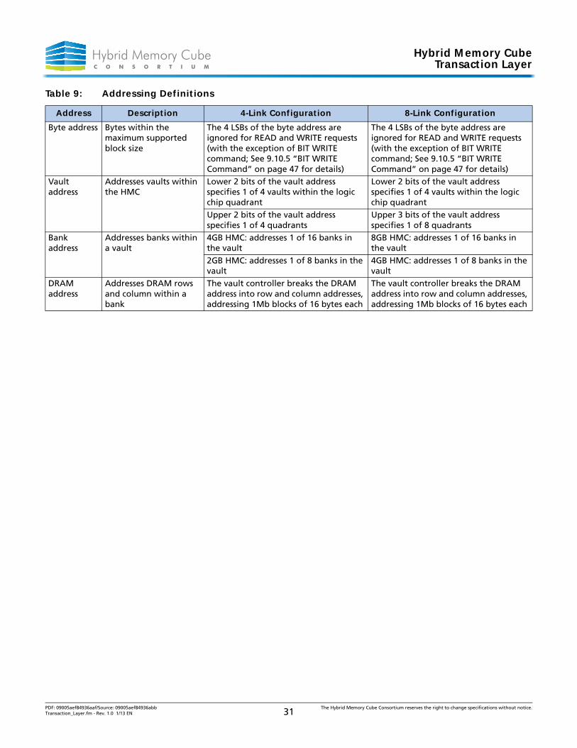
Hybrid Memory CubeTransaction Layer
Table 9: Addressing Definitions
Address Description 4-Link Configuration 8-Link Configuration
Byte address Bytes within the maximum supported block size
The 4 LSBs of the byte address are ignored for READ and WRITE requests (with the exception of BIT WRITE command; See 9.10.5 “BIT WRITE Command” on page 47 for details)
The 4 LSBs of the byte address are ignored for READ and WRITE requests (with the exception of BIT WRITE command; See 9.10.5 “BIT WRITE Command” on page 47 for details)
Vault address
Addresses vaults within the HMC
Lower 2 bits of the vault address specifies 1 of 4 vaults within the logic chip quadrant
Lower 2 bits of the vault address specifies 1 of 4 vaults within the logic chip quadrant
Upper 2 bits of the vault address specifies 1 of 4 quadrants
Upper 3 bits of the vault address specifies 1 of 8 quadrants
Bank address
Addresses banks within a vault
4GB HMC: addresses 1 of 16 banks in the vault
8GB HMC: addresses 1 of 16 banks in the vault
2GB HMC: addresses 1 of 8 banks in the vault
4GB HMC: addresses 1 of 8 banks in the vault
DRAM address
Addresses DRAM rows and column within a bank
The vault controller breaks the DRAM address into row and column addresses, addressing 1Mb blocks of 16 bytes each
The vault controller breaks the DRAM address into row and column addresses, addressing 1Mb blocks of 16 bytes each
PDF: 09005aef84936aaf/Source: 09005aef84936abb The Hybrid Memory Cube Consortium reserves the right to change specifications without notice.Transaction_Layer.fm - Rev. 1.0 1/13 EN 31

Hybrid Memory CubeTransaction Layer
9.1.3 Default Address-Map Mode Table – 4-link Devices
Table 10: Default Address Map Mode Table
Request Address
Bit
2GB – 4 Link Device 4GB – 4 Link Device
32-Byte Max Block Size
64-Byte Max Block Size
128-Byte Max Block Size
32-Byte Max Block Size
64-Byte Max Block Size
128-Byte Max Block Size
33 Ignored Ignored Ignored Ignored Ignored Ignored
32 Ignored Ignored Ignored Ignored Ignored Ignored
31 Ignored Ignored Ignored DRAM[19] DRAM[19] DRAM[19]
30 DRAM[19] DRAM[19] DRAM[19] DRAM[18] DRAM[18] DRAM[18]
29 DRAM[18] DRAM[18] DRAM[18] DRAM[17] DRAM[17] DRAM[17]
28 DRAM[17] DRAM[17] DRAM[17] DRAM[16] DRAM[16] DRAM[16]
27 DRAM[16] DRAM[16] DRAM[16] DRAM[15] DRAM[15] DRAM[15]
26 DRAM[15] DRAM[15] DRAM[15] DRAM[14] DRAM[14] DRAM[14]
25 DRAM[14] DRAM[14] DRAM[14] DRAM[13] DRAM[13] DRAM[13]
24 DRAM[13] DRAM[13] DRAM[13] DRAM[12] DRAM[12] DRAM[12]
23 DRAM[12] DRAM[12] DRAM[12] DRAM[11] DRAM[11] DRAM[11]
22 DRAM[11] DRAM[11] DRAM[11] DRAM[10] DRAM[10] DRAM[10]
21 DRAM[10] DRAM[10] DRAM[10] DRAM[9] DRAM[9] DRAM[9]
20 DRAM[9] DRAM[9] DRAM[9] DRAM[8] DRAM[8] DRAM[8]
19 DRAM[8] DRAM[8] DRAM[8] DRAM[7] DRAM[7] DRAM[7]
18 DRAM[7] DRAM[7] DRAM[7] DRAM[6] DRAM[6] DRAM[6]
17 DRAM[6] DRAM[6] DRAM[6] DRAM[5] DRAM[5] DRAM[5]
16 DRAM[5] DRAM[5] DRAM[5] DRAM[4] DRAM[4] DRAM[4]
15 DRAM[4] DRAM[4] DRAM[4] DRAM[3] DRAM[3] DRAM[3]
14 DRAM[3] DRAM[3] DRAM[3] DRAM[2] DRAM[2] Bank[3]
13 DRAM[2] DRAM[2] Bank[2] DRAM[1] Bank[3] Bank[2]
12 DRAM[1] Bank[2] Bank[1] Bank[3] Bank[2] Bank[1]
11 Bank[2] Bank[1] Bank[0] Bank[2] Bank[1] Bank[0]
10 Bank[1] Bank[0] Vault[3] Bank[1] Bank[0] Vault[3]
9 Bank[0] Vault[3] Vault[2] Bank[0] Vault[3] Vault[2]
8 Vault[3] Vault[2] Vault[1] Vault[3] Vault[2] Vault[1]
7 Vault[2] Vault[1] Vault[0] Vault[2] Vault[1] Vault[0]
6 Vault[1] Vault[0] Byte[6], DRAM[2] Vault[1] Vault[0] Byte[6], DRAM[2]
5 Vault[0] Byte[5], DRAM[1] Byte[5], DRAM[1] Vault[0] Byte[5], DRAM[1] Byte[5], DRAM[1]
4 Byte[4], DRAM[0] Byte[4], DRAM[0] Byte[4], DRAM[0] Byte[4], DRAM[0] Byte[4], DRAM[0] Byte[4], DRAM[0]
3 Byte[3] = Ignored Byte[3] = Ignored Byte[3] = Ignored Byte[3] = Ignored Byte[3] = Ignored Byte[3] = Ignored
2 Byte[2] = Ignored Byte[2] = Ignored Byte[2] = Ignored Byte[2] = Ignored Byte[2] = Ignored Byte[2] = Ignored
1 Byte[1] = Ignored Byte[1] = Ignored Byte[1] = Ignored Byte[1] = Ignored Byte[1] = Ignored Byte[1] = Ignored
0 Byte[0] = Ignored Byte[0] = Ignored Byte[0] = Ignored Byte[0] = Ignored Byte[0] = Ignored Byte[0] = Ignored
PDF: 09005aef84936aaf/Source: 09005aef84936abb The Hybrid Memory Cube Consortium reserves the right to change specifications without notice.Transaction_Layer.fm - Rev. 1.0 1/13 EN 32
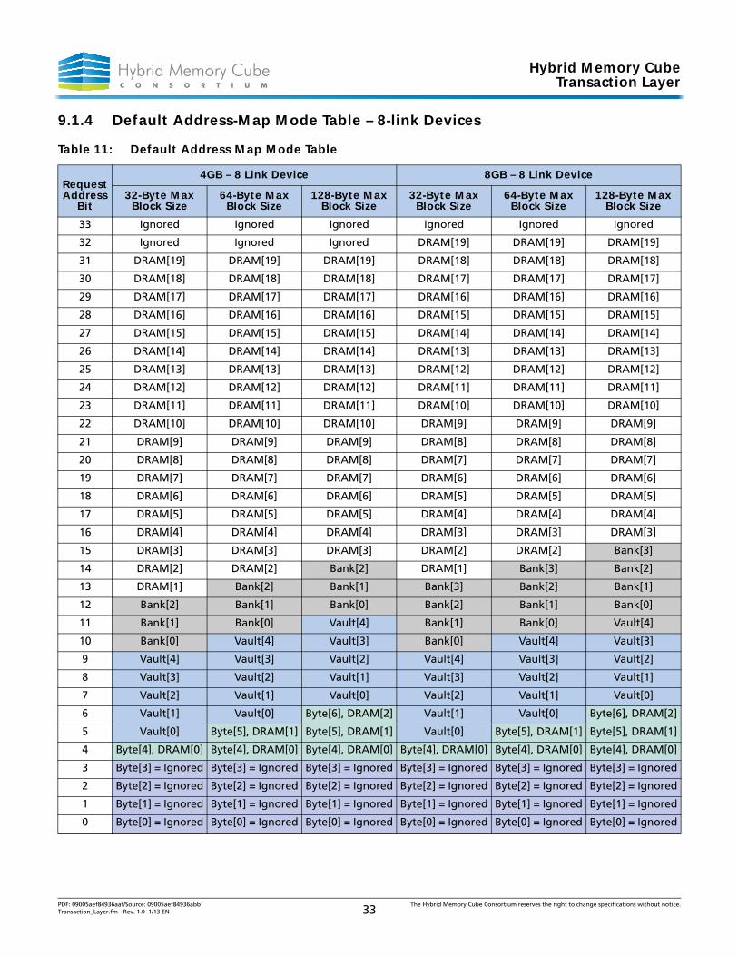
Hybrid Memory CubeTransaction Layer
9.1.4 Default Address-Map Mode Table – 8-link Devices
Table 11: Default Address Map Mode Table
Request Address
Bit
4GB – 8 Link Device 8GB – 8 Link Device
32-Byte Max Block Size
64-Byte Max Block Size
128-Byte Max Block Size
32-Byte Max Block Size
64-Byte Max Block Size
128-Byte Max Block Size
33 Ignored Ignored Ignored Ignored Ignored Ignored
32 Ignored Ignored Ignored DRAM[19] DRAM[19] DRAM[19]
31 DRAM[19] DRAM[19] DRAM[19] DRAM[18] DRAM[18] DRAM[18]
30 DRAM[18] DRAM[18] DRAM[18] DRAM[17] DRAM[17] DRAM[17]
29 DRAM[17] DRAM[17] DRAM[17] DRAM[16] DRAM[16] DRAM[16]
28 DRAM[16] DRAM[16] DRAM[16] DRAM[15] DRAM[15] DRAM[15]
27 DRAM[15] DRAM[15] DRAM[15] DRAM[14] DRAM[14] DRAM[14]
26 DRAM[14] DRAM[14] DRAM[14] DRAM[13] DRAM[13] DRAM[13]
25 DRAM[13] DRAM[13] DRAM[13] DRAM[12] DRAM[12] DRAM[12]
24 DRAM[12] DRAM[12] DRAM[12] DRAM[11] DRAM[11] DRAM[11]
23 DRAM[11] DRAM[11] DRAM[11] DRAM[10] DRAM[10] DRAM[10]
22 DRAM[10] DRAM[10] DRAM[10] DRAM[9] DRAM[9] DRAM[9]
21 DRAM[9] DRAM[9] DRAM[9] DRAM[8] DRAM[8] DRAM[8]
20 DRAM[8] DRAM[8] DRAM[8] DRAM[7] DRAM[7] DRAM[7]
19 DRAM[7] DRAM[7] DRAM[7] DRAM[6] DRAM[6] DRAM[6]
18 DRAM[6] DRAM[6] DRAM[6] DRAM[5] DRAM[5] DRAM[5]
17 DRAM[5] DRAM[5] DRAM[5] DRAM[4] DRAM[4] DRAM[4]
16 DRAM[4] DRAM[4] DRAM[4] DRAM[3] DRAM[3] DRAM[3]
15 DRAM[3] DRAM[3] DRAM[3] DRAM[2] DRAM[2] Bank[3]
14 DRAM[2] DRAM[2] Bank[2] DRAM[1] Bank[3] Bank[2]
13 DRAM[1] Bank[2] Bank[1] Bank[3] Bank[2] Bank[1]
12 Bank[2] Bank[1] Bank[0] Bank[2] Bank[1] Bank[0]
11 Bank[1] Bank[0] Vault[4] Bank[1] Bank[0] Vault[4]
10 Bank[0] Vault[4] Vault[3] Bank[0] Vault[4] Vault[3]
9 Vault[4] Vault[3] Vault[2] Vault[4] Vault[3] Vault[2]
8 Vault[3] Vault[2] Vault[1] Vault[3] Vault[2] Vault[1]
7 Vault[2] Vault[1] Vault[0] Vault[2] Vault[1] Vault[0]
6 Vault[1] Vault[0] Byte[6], DRAM[2] Vault[1] Vault[0] Byte[6], DRAM[2]
5 Vault[0] Byte[5], DRAM[1] Byte[5], DRAM[1] Vault[0] Byte[5], DRAM[1] Byte[5], DRAM[1]
4 Byte[4], DRAM[0] Byte[4], DRAM[0] Byte[4], DRAM[0] Byte[4], DRAM[0] Byte[4], DRAM[0] Byte[4], DRAM[0]
3 Byte[3] = Ignored Byte[3] = Ignored Byte[3] = Ignored Byte[3] = Ignored Byte[3] = Ignored Byte[3] = Ignored
2 Byte[2] = Ignored Byte[2] = Ignored Byte[2] = Ignored Byte[2] = Ignored Byte[2] = Ignored Byte[2] = Ignored
1 Byte[1] = Ignored Byte[1] = Ignored Byte[1] = Ignored Byte[1] = Ignored Byte[1] = Ignored Byte[1] = Ignored
0 Byte[0] = Ignored Byte[0] = Ignored Byte[0] = Ignored Byte[0] = Ignored Byte[0] = Ignored Byte[0] = Ignored
PDF: 09005aef84936aaf/Source: 09005aef84936abb The Hybrid Memory Cube Consortium reserves the right to change specifications without notice.Transaction_Layer.fm - Rev. 1.0 1/13 EN 33
Hybrid Memory CubeTransaction Layer
9.1.5 Address Mapping Mode Register
The address mapping mode register provides user control of mapping portions of the ADRS field within the header of request packets to the vault and bank addresses. When using default address-mapping, the address mapping mode field should be set based on specific system requirements. See Section 14.2 “Data Access Performance Consider-ations” on page 76 for details.
In addition to the default address mapping algorithms, user-defined fields are provided for the user to specify a unique mapping algorithm. There is a user-defined field for the vault address and the bank address. Each field holds a 5-bit encoded value pointing to the corresponding bit position in the ADRS field of the request packet header. This represents the LSB that will be used for the vault or bank address, with the more signifi-cant bits of the subaddress coming from the bit positions immediately above it in the request header ADRS field. When operating with the user-defined modes, it is the user’s responsibility to set the user-defined encoded fields so that the vault and bank addresses do not overlap each other or overlap the byte address within the request header ADRS field. Note that the byte address is always fixed at the LSBs of the request header ADRS field. The user must also be aware that the number of bits in the bank address is depen-dent upon the size of the HMC. The remaining bits of the request ADRS field not speci-fied as the vault and bank addresses become the DRAM address. See Section 10 “Configuration and Status Registers” for more details on user-defined address mapping.
The address map mode register is writable via the MODE WRITE command or via the maintenance interface (I2C or JTAG bus). Note that because the MAX block size is defaulted to 64 bytes, the host boot block code must either be compatible (issue requests of 64 bytes or smaller) or issue a MODE WRITE command to change the MAX block size.
9.1.6 DRAM Addressing
Each bank in the HMC contains 16,777,216 memory bytes (16 MB). A WRITE or READ command to a bank accesses 32 bytes of data for each column fetch. The bank configu-ration is identical in all specified HMC configurations.
9.2 Packet Length
As noted previously, packets are always multiples of 16-byte FLITs. Within each packet header there is a length (LNG) field that indicates the total number of FLITs in the packet. A packet that contains no data FLITs would have LNG = 1; this represents the single FLIT holding the 8-byte header and 8-byte tail. When generating response packets, the necessary data size is determined from the CMD field in the corresponding request packet. Specific packet lengths are provided in the Tables 17, 25, and 26.
A Duplicate Length (DLN) field is included within each packet header to provide addi-tional packet integrity. The value of DLN must equal that of LNG within a packet. The DLN field is compared to the LNG field prior to the CRC being checked. Note that LNG enables the packet parser to determine the location of the CRC field (where a value of 1 points to the current FLIT). A miscompare of DLN and LNG is treated like a CRC check and will trigger the link retry mechanism. If LNG does not equal DLN when the packet is generated at the host, link retries will be unsuccessful and a fatal error will result.
PDF: 09005aef84936aaf/Source: 09005aef84936abb The Hybrid Memory Cube Consortium reserves the right to change specifications without notice.Transaction_Layer.fm - Rev. 1.0 1/13 EN 34
Hybrid Memory CubeTransaction Layer
9.3 Packet Flow Control
Flow control occurs in both directions on each link. The flow of transaction layer packets is managed with token counts. Each token represents the storage to hold one FLIT (16 bytes). The link slave input buffer temporarily stores transaction layer packets as they are received from the link. (Note that flow packets are not stored in the input buffer, and therefore, are not subject to flow control.) The minimum size of this buffer must be equal to or greater than the number of FLITs in a single packet of the largest supported length, but in general can hold several of the largest packets to enable a constant flow across the link. The available space in this input buffer is represented in a token count register at the link master. This gives the link master knowledge of the available buffering at the other end of the link and the ability to evaluate whether there is enough buffer space to receive every FLIT of the next packet to be transmitted.
The token count register is loaded during the initialization sequence with the maximum number of tokens representing the available buffer space at the link slave when it is empty. As the link master sends each transaction layer packet across the link, it must decrement the token count register by the number of FLITs in the transmitted packet. As the packet is received and stored in the input buffer, its FLITs use up the space repre-sented by the decremented value of token count register at the link master. As each packet is read out of the input buffer, it is forwarded to a destination, and its FLIT loca-tion is freed up. This requires a mechanism to return packet tokens to the link trans-mitter, using the opposite link direction. The input buffer control logic sends a count (representing the number of FLITs that were read out of the input buffer when the packet was forwarded) to the local (adjacent) link master. This count is returned in the return token count (RTC) field of the next possible packet traveling in the opposite direc-tion on the link. At the link slave, the RTC field is extracted from the incoming packet and sent back to the original link transmitter where its value is added to the current value of the token count register. If no transaction layer packet traffic is occurring in the return direction, the link master must create a flow packet known as a token return (TRET) to return the token. TRET is described in 9.12.3 “TOKEN RETURN (TRET) Command” on page 50.
Appropriate sizing of the link slave input buffer requires weighing the trade-offs between latency, throughput, silicon real-estate, and routability. If there is a temporary pause in the packet forwarding priority at the output of the input buffer (internal switch conflicts, or destination vault flow control), a packet might not be emptied from the input buffer. This would cause a pause in the return of the tokens. As long as this is infrequent and the input buffer is sized to accommodate it, the packet flow will not be disrupted unless the link is running at 100% busy. If the input buffer is empty, a specific implementation may choose to bypass the input buffer and forward a packet immediately to its destination. In this case, the tokens for the packet would be immediately returned to the link master.
As noted previously, the link master must not transmit a packet if there is insufficient space in the input buffer at the other end of the link. The LNG field within the header of each outgoing packet must be compared to the token count register to determine whether the packet should be transmitted or the packet stream should be paused.
9.4 Tagging
Operational closure for requests is accomplished using the tag fields in request and response packets. The tag value remains associated with the request until a response is received indicating that the request has been executed. Tags in READ requests are returned with the respective read data in the read response packet header. Write
PDF: 09005aef84936aaf/Source: 09005aef84936abb The Hybrid Memory Cube Consortium reserves the right to change specifications without notice.Transaction_Layer.fm - Rev. 1.0 1/13 EN 35
Hybrid Memory CubeTransaction Layer
response tags are returned either within a write response packet, or optionally within the return tag A (TGA) field of any other response packet being returned to the same source link. If the feature is not supported, the corresponding bits within response packets will be specified as reserved. In the case of posted write requests, because no response is returned and the HMC does not use the TAG field of posted write requests, the host can populate this field with any value. Note that when multiple host links are connected to the HMC, each response packet will be returned on the same link as its associated request. This keeps the tag range independent for each host link.
Tag fields in packets are nine bits long, which is enough space for 512 tags. All tags are available for use. Tag assignment and reassignment are managed by the host. There is no required algorithm to assign tag values to requests. HMC does not use the tag for internal control or identification, only for copying the tag from the request packet to the response packet.
Tags are assigned by control logic at the host link master and must not be used in another request packet until a response tag with the same tag number is returned to that host link. Other host links will use the same tag range of 512 tags, but they are uniquely identified by their association with each different host link. Thus, the total maximum number of unique tags is 512 times the number of host links. For example, if four links are connected from an HMC to the host, there are 2048 usable tags for requests to the HMC. As an implementation example, a host control logic might decide to provide a time-out capability for every transaction to determine whether a request or response packet has been lost or corrupted, preventing the tag from being returned. The timer in this implementation example would consider link retry periods that occur to account for response packets that are delayed, but still returned.
9.5 Packet Integrity
The integrity of the packet contents is maintained with the CRC field in the tail of every packet. Because the entire packet (including header and tail) is transmitted from the source link all of the way to the destination vault, CRC is used to detect failures that occur not only on transmission across the link, but along the entire path. Note that CRC may be regenerated along the path if flow control fields within the header or tail change. CRC regeneration is done in an overlapped fashion with respect to a CRC check to ensure that no single point of failure will go undetected.
There may be cases when the first FLITs of a packet are forwarded before the tail is received and the CRC is checked. This may occur in the HMC’s link slave after a request packet crosses a link and is done to avoid adding latency in the packet path. If the packet is found to have a CRC error as it passes through the link slave, the packet is “poisoned," meaning that a destination, in this case a vault controller, will recognize it as nonfunc-tional and will not use it. The link slave poisons the packet by inverting a recalculated value of the CRC and inserting that into the tail in place of the errored CRC. Another example of a forwarded poisoned packet is the case in which DRAM errors occur and are internally retried. If a parity error occurs on the command or address from the vault controller to the DRAM, a response packet may be generated and transmission back to the requester could be started before the parity error is detected. In this case, the CRC in the tail of the response packet will be poisoned, meaning the vault controller will invert the CRC and insert it into the tail of the packet. Consequently, the requester may receive the poisoned packet and must drop it. The vault controller will retry the DRAM request, and upon a successful DRAM access, another response packet will be generated to replace the poisoned one.
PDF: 09005aef84936aaf/Source: 09005aef84936abb The Hybrid Memory Cube Consortium reserves the right to change specifications without notice.Transaction_Layer.fm - Rev. 1.0 1/13 EN 36
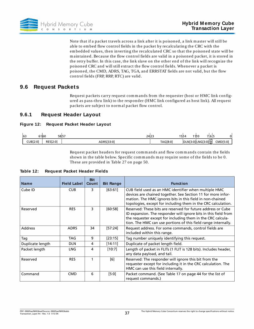
Hybrid Memory CubeTransaction Layer
Note that if a packet travels across a link after it is poisoned, a link master will still be able to embed flow control fields in the packet by recalculating the CRC with the embedded values, then inverting the recalculated CRC so that the poisoned state will be maintained. Because the flow control fields are valid in a poisoned packet, it is stored in the retry buffer. In this case, the link slave on the other end of the link will recognize the poisoned CRC and will still extract the flow control fields. Whenever a packet is poisoned, the CMD, ADRS, TAG, TGA, and ERRSTAT fields are not valid, but the flow control fields (FRP, RRP, RTC) are valid.
9.6 Request Packets
Request packets carry request commands from the requester (host or HMC link config-ured as pass-thru link) to the responder (HMC link configured as host link). All request packets are subject to normal packet flow control.
9.6.1 Request Header Layout
Figure 12: Request Packet Header Layout
Request packet headers for request commands and flow commands contain the fields shown in the table below. Specific commands may require some of the fields to be 0. These are provided in Table 27 on page 50.
Table 12: Request Packet Header Fields
Name Field LabelBit
Count Bit Range Function
Cube ID CUB 3 [63:61] CUB field used as an HMC identifier when multiple HMC devices are chained together. See Section 11 for more infor-mation. The HMC ignores bits in this field in non-chained topologies, except for including them in the CRC calculation.
Reserved RES 3 [60:58] Reserved: These bits are reserved for future address or Cube ID expansion. The responder will ignore bits in this field from the requester except for including them in the CRC calcula-tion. The HMC can use portions of this field range internally.
Address ADRS 34 [57:24] Request address. For some commands, control fields are included within this range.
Tag TAG 9 [23:15] Tag number uniquely identifying this request.Duplicate length DLN 4 [14:11] Duplicate of packet length field.Packet length LNG 4 [10:7] Length of packet in FLITs (1 FLIT is 128 bits). Includes header,
any data payload, and tail.Reserved RES 1 [6] Reserved: The responder will ignore this bit from the
requester except for including it in the CRC calculation. The HMC can use this field internally.
Command CMD 6 [5:0] Packet command. (See Table 17 on page 44 for the list of request commands.)
60 58 57 24 23 15 101114 07 6 5
ADRS[33:0]RES[2:0]
63 61
CUB[2:0] TAG[8:0] DLN[3:0] LNG[3:0] CMD[5:0]RES
PDF: 09005aef84936aaf/Source: 09005aef84936abb The Hybrid Memory Cube Consortium reserves the right to change specifications without notice.Transaction_Layer.fm - Rev. 1.0 1/13 EN 37
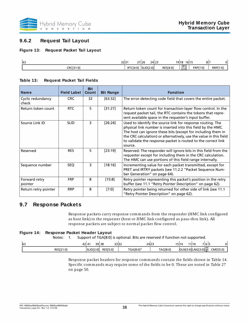
Hybrid Memory CubeTransaction Layer
9.6.2 Request Tail Layout
Figure 13: Request Packet Tail Layout
9.7 Response Packets
Response packets carry response commands from the responder (HMC link configured as host link) to the requester (host or HMC link configured as pass-thru link). All response packets are subject to normal packet flow control.
Figure 14: Response Packet Header LayoutNotes: 1. Support of TGA[8:0] is optional. Bits are reserved if function not supported.
Response packet headers for response commands contain the fields shown in Table 14. Specific commands may require some of the fields to be 0. These are noted in Table 27 on page 50.
Table 13: Request Packet Tail Fields
Name Field LabelBit
Count Bit Range Function
Cyclic redundancy check
CRC 32 [63:32] The error-detecting code field that covers the entire packet.
Return token count RTC 5 [31:27] Return token count for transaction-layer flow control. In the request packet tail, the RTC contains the tokens that repre-sent available space in the requester’s input buffer.
Source Link ID SLID 3 [26:24] Used to identify the source link for response routing. The physical link number is inserted into this field by the HMC. The host can ignore these bits (except for including them in the CRC calculation) or alternatively, use the value in this field to validate the response packet is routed to the correct link source.
Reserved RES 5 [23:19] Reserved: The responder will ignore bits in this field from the requester except for including them in the CRC calculation. The HMC can use portions of this field range internally.
Sequence number SEQ 3 [18:16] Incrementing value for each packet transmitted, except for PRET and IRTRY packets (see 11.2.2 “Packet Sequence Num-ber Generation” on page 64).
Forward retry pointer
FRP 8 [15:8] Retry pointer representing this packet’s position in the retry buffer (see 11.1 “Retry Pointer Description” on page 62).
Return retry pointer RRP 8 [7:0] Retry pointer being returned for other side of link (see 11.1 “Retry Pointer Description” on page 62).
63 32 31 26 24 2327 15161819 078
CRC[31:0] RTC[4:0] SLID[2:0] RES[4:0]SEQ[2:0] FRP[7:0] RRP[7:0]
63 3338394142 32 24 101115 14 023 567
RES[5:0]RES[21:0] SLID[2:0] TGA[8:0]1 TAG[8:0] DLN[3:0] LNG[3:0] CMD[5:0]RES
PDF: 09005aef84936aaf/Source: 09005aef84936abb The Hybrid Memory Cube Consortium reserves the right to change specifications without notice.Transaction_Layer.fm - Rev. 1.0 1/13 EN 38
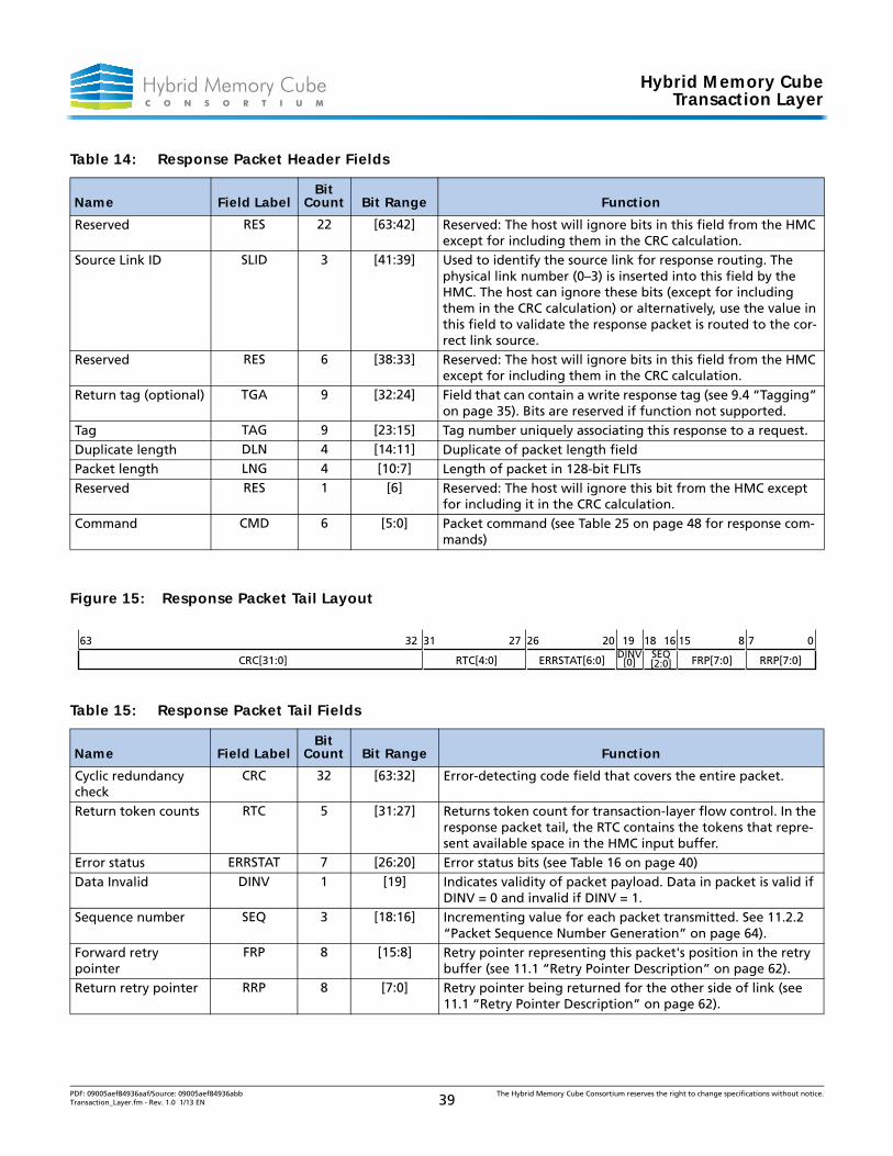
Hybrid Memory CubeTransaction Layer
Figure 15: Response Packet Tail Layout
Table 14: Response Packet Header Fields
Name Field LabelBit
Count Bit Range Function
Reserved RES 22 [63:42] Reserved: The host will ignore bits in this field from the HMC except for including them in the CRC calculation.
Source Link ID SLID 3 [41:39] Used to identify the source link for response routing. The physical link number (0–3) is inserted into this field by the HMC. The host can ignore these bits (except for including them in the CRC calculation) or alternatively, use the value in this field to validate the response packet is routed to the cor-rect link source.
Reserved RES 6 [38:33] Reserved: The host will ignore bits in this field from the HMC except for including them in the CRC calculation.
Return tag (optional) TGA 9 [32:24] Field that can contain a write response tag (see 9.4 “Tagging” on page 35). Bits are reserved if function not supported.
Tag TAG 9 [23:15] Tag number uniquely associating this response to a request.Duplicate length DLN 4 [14:11] Duplicate of packet length fieldPacket length LNG 4 [10:7] Length of packet in 128-bit FLITsReserved RES 1 [6] Reserved: The host will ignore this bit from the HMC except
for including it in the CRC calculation.Command CMD 6 [5:0] Packet command (see Table 25 on page 48 for response com-
mands)
Table 15: Response Packet Tail Fields
Name Field LabelBit
Count Bit Range Function
Cyclic redundancy check
CRC 32 [63:32] Error-detecting code field that covers the entire packet.
Return token counts RTC 5 [31:27] Returns token count for transaction-layer flow control. In the response packet tail, the RTC contains the tokens that repre-sent available space in the HMC input buffer.
Error status ERRSTAT 7 [26:20] Error status bits (see Table 16 on page 40)Data Invalid DINV 1 [19] Indicates validity of packet payload. Data in packet is valid if
DINV = 0 and invalid if DINV = 1.Sequence number SEQ 3 [18:16] Incrementing value for each packet transmitted. See 11.2.2
“Packet Sequence Number Generation” on page 64).Forward retry pointer
FRP 8 [15:8] Retry pointer representing this packet's position in the retry buffer (see 11.1 “Retry Pointer Description” on page 62).
Return retry pointer RRP 8 [7:0] Retry pointer being returned for the other side of link (see 11.1 “Retry Pointer Description” on page 62).
63 32 31 1516181920 02627 78
CRC[31:0] RTC[4:0]DINV
[0]ERRSTAT[6:0]SEQ[2:0] FRP[7:0] RRP[7:0]
PDF: 09005aef84936aaf/Source: 09005aef84936abb The Hybrid Memory Cube Consortium reserves the right to change specifications without notice.Transaction_Layer.fm - Rev. 1.0 1/13 EN 39
Hybrid Memory CubeTransaction Layer
The ERRSTAT field included in the response tail is valid for all read, write, and error responses. All bits in the ERRSTAT field being zero indicates a normal response with no errors or flags. There are 6 different error and flag categories defined by ERRSTAT[6:4] bits. The unique error or flag descriptions within each category indicate a specific error or item that requires attention. Additional status on errors or flags can be obtained by accessing internal status registers using the MODE READ command or sideband (I2C or JTAG). Table 16 shows the error categories and descriptions along with the method of response (read/write response packet or error response packet).
Table 16: ERRSTAT[6:0] Bit Definitions
ERRSTAT Bit
Description Response Packet Type6 5 4 3 2 1 0
0 0 0 0 0 0 0 No errors/conditionsWarnings
0 0 0 0 0 0 1 Operational temperature threshold: The internal temperature sensors in the HMC have reached the upper limits of operational temperature.
Error response packet(TAG = CUB number)
0 0 0 0 0 1 0 Host token overflow warning: The host sent more than 1023 tokens to the HMC on a link.
0 0 0 0 1 0 0 Repair information (optional): Remaining repair resources have fallen below a minimum threshold.
0 0 0 0 1 0 1 Repair warning (optional): There are one or more regions of memory that have no available repair resources left.
0 0 0 0 1 1 0 Repair alarm: A request has encountered a hard SBE or MUE, and there are no repair resources available.
DRAM Errors0 0 1 0 0 0 0 SBE occurred (this status is normally disabled) -
Data is corrected before being returned to the requester. the SBE is scrubbed and tested to determine if it is a hard error, in which case it is dynamically repaired.
Read or write response packet(TAG = tag of corresponding request)
0 0 1 1 1 1 1 MUE has occurred - this indicates that a multiple uncorrectable error has occurred in the DRAM for read data. The DINV (data invalid) flag will also be active. Can also be unsolicited if MUE encountered during patrol scrub.
Link Errors
PDF: 09005aef84936aaf/Source: 09005aef84936abb The Hybrid Memory Cube Consortium reserves the right to change specifications without notice.Transaction_Layer.fm - Rev. 1.0 1/13 EN 40

Hybrid Memory CubeTransaction Layer
0 1 0 0 0 0 0 Link 0 retry successful: Link 0 has successfully recovered from a link error by executing one or more link retries (within the retry attempt limit).
Error response packet(TAG = CUB number)
0 1 0 0 0 0 1 Link 1retry successful: Link 1 has successfully recovered from a link error by executing one or more link retries (within the retry attempt limit).
0 1 0 0 0 1 0 Link 2 retry successful: Link 2 has successfully recovered from a link error by executing one or more link retries (within the retry attempt limit).
0 1 0 0 0 1 1 Link 3 retry successful: Link 3 has successfully recovered from a link error by executing one or more link retries (within the retry attempt limit).
0 1 0 0 1 0 0 Link 4 retry successful: Link 4 has successfully recovered from a link error by executing one or more link retries (within the retry attempt limit).
0 1 0 0 1 0 1 Link 5 retry successful: Link 5 has successfully recovered from a link error by executing one or more link retries (within the retry attempt limit).
0 1 0 0 1 1 0 Link 6 retry successful: Link 6 has successfully recovered from a link error by executing one or more link retries (within the retry attempt limit).
0 1 0 0 1 1 1 Link 7 retry successful: Link7 has successfully recovered from a link error by executing one or more link retries (within the retry attempt limit).
Error response packet(TAG = CUB number)
Protocol Errors0 1 1 0 0 0 0 Invalid command: An unsupported command
existed in a request packet. Write response packet(TAG = tag of corresponding request)
0 1 1 0 0 0 1 Invalid length: An invalid length was specified for the given command in a request packet.
Read response packet(TAG = tag of corresponding request)
Vault Critical Errors
Table 16: ERRSTAT[6:0] Bit Definitions (Continued)
ERRSTAT Bit
Description Response Packet Type6 5 4 3 2 1 0
PDF: 09005aef84936aaf/Source: 09005aef84936abb The Hybrid Memory Cube Consortium reserves the right to change specifications without notice.Transaction_Layer.fm - Rev. 1.0 1/13 EN 41
Hybrid Memory CubeTransaction Layer
1 1 0 0 0 0 0 Vault 0 critical error: Command/Address parity error has not cleared after the command/address retry count threshold has been met. Vault 0 command execution is halted until a reset is performed.
Error response packet(TAG = CUB number)
1 1 0 0 0 0 1 Vault 1 critical error1 1 0 0 0 1 0 Vault 2 critical error1 1 0 0 0 1 1 Vault 3 critical error1 1 0 0 1 0 0 Vault 4 critical error1 1 0 0 1 0 1 Vault 5 critical error1 1 0 0 1 1 0 Vault 6 critical error1 1 0 0 1 1 1 Vault 7 critical error1 1 0 1 0 0 0 Vault 8 critical error1 1 0 1 0 0 1 Vault 9 critical error1 1 0 1 0 1 0 Vault 10 critical error1 1 0 1 0 1 1 Vault 11 critical error1 1 0 1 1 0 0 Vault 12 critical error1 1 0 1 1 0 1 Vault 13 critical error1 1 0 1 1 1 0 Vault 14 critical error1 1 0 1 1 1 1 Vault 15 critical error1 0 1 0 0 0 0 Vault 16 critical error (8-link device only)1 0 1 ... ... ... ... Vault 17–30 (8-link device only); Increment
ERRSTAT[3:0] sequentially for each incrementing vault.
1 0 1 1 1 1 1 Vault 31 (8-link device only)Fatal Errors
1 1 1 0 0 0 0 Link 0 retry failed and was unsuccessful after the retry limit was reached.
Error response packet(TAG = CUB number)
1 1 1 0 0 0 1 Link 1 retry failed and was unsuccessful after the retry limit was reached.
1 1 1 0 0 1 0 Link 2 retry failed and was unsuccessful after the retry limit was reached.
1 1 1 0 0 1 1 Link 3 retry failed and was unsuccessful after the retry limit was reached.
1 1 1 0 1 0 0 Link 4 retry failed and was unsuccessful after the retry limit was reached.
1 1 1 0 1 0 1 Link 5 retry failed and was unsuccessful after the retry limit was reached.
1 1 1 0 1 1 0 Link 6 retry failed and was unsuccessful after the retry limit was reached.
1 1 1 0 1 1 1 Link 7 retry failed and was unsuccessful after the retry limit was reached.
Table 16: ERRSTAT[6:0] Bit Definitions (Continued)
ERRSTAT Bit
Description Response Packet Type6 5 4 3 2 1 0
PDF: 09005aef84936aaf/Source: 09005aef84936abb The Hybrid Memory Cube Consortium reserves the right to change specifications without notice.Transaction_Layer.fm - Rev. 1.0 1/13 EN 42
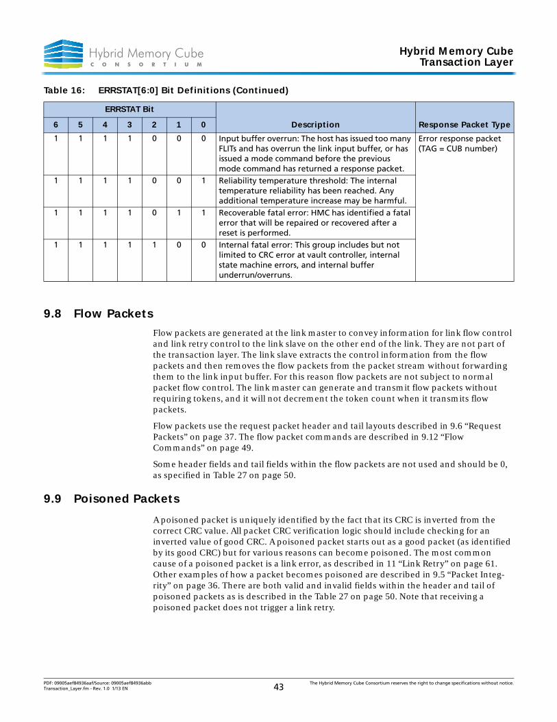
Hybrid Memory CubeTransaction Layer
9.8 Flow Packets
Flow packets are generated at the link master to convey information for link flow control and link retry control to the link slave on the other end of the link. They are not part of the transaction layer. The link slave extracts the control information from the flow packets and then removes the flow packets from the packet stream without forwarding them to the link input buffer. For this reason flow packets are not subject to normal packet flow control. The link master can generate and transmit flow packets without requiring tokens, and it will not decrement the token count when it transmits flow packets.
Flow packets use the request packet header and tail layouts described in 9.6 “Request Packets” on page 37. The flow packet commands are described in 9.12 “Flow Commands” on page 49.
Some header fields and tail fields within the flow packets are not used and should be 0, as specified in Table 27 on page 50.
9.9 Poisoned Packets
A poisoned packet is uniquely identified by the fact that its CRC is inverted from the correct CRC value. All packet CRC verification logic should include checking for an inverted value of good CRC. A poisoned packet starts out as a good packet (as identified by its good CRC) but for various reasons can become poisoned. The most common cause of a poisoned packet is a link error, as described in 11 “Link Retry” on page 61. Other examples of how a packet becomes poisoned are described in 9.5 “Packet Integ-rity” on page 36. There are both valid and invalid fields within the header and tail of poisoned packets as is described in the Table 27 on page 50. Note that receiving a poisoned packet does not trigger a link retry.
1 1 1 1 0 0 0 Input buffer overrun: The host has issued too many FLITs and has overrun the link input buffer, or has issued a mode command before the previous mode command has returned a response packet.
Error response packet(TAG = CUB number)
1 1 1 1 0 0 1 Reliability temperature threshold: The internal temperature reliability has been reached. Any additional temperature increase may be harmful.
1 1 1 1 0 1 1 Recoverable fatal error: HMC has identified a fatal error that will be repaired or recovered after a reset is performed.
1 1 1 1 1 0 0 Internal fatal error: This group includes but not limited to CRC error at vault controller, internal state machine errors, and internal buffer underrun/overruns.
Table 16: ERRSTAT[6:0] Bit Definitions (Continued)
ERRSTAT Bit
Description Response Packet Type6 5 4 3 2 1 0
PDF: 09005aef84936aaf/Source: 09005aef84936abb The Hybrid Memory Cube Consortium reserves the right to change specifications without notice.Transaction_Layer.fm - Rev. 1.0 1/13 EN 43
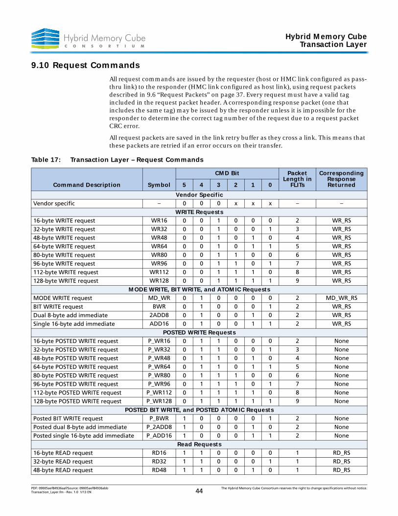
Hybrid Memory CubeTransaction Layer
9.10 Request Commands
All request commands are issued by the requester (host or HMC link configured as pass-thru link) to the responder (HMC link configured as host link), using request packets described in 9.6 “Request Packets” on page 37. Every request must have a valid tag included in the request packet header. A corresponding response packet (one that includes the same tag) may be issued by the responder unless it is impossible for the responder to determine the correct tag number of the request due to a request packet CRC error.
All request packets are saved in the link retry buffer as they cross a link. This means that these packets are retried if an error occurs on their transfer.
Table 17: Transaction Layer – Request Commands
Command Description Symbol
CMD Bit Packet Length in
FLITs
Corresponding Response Returned5 4 3 2 1 0
Vendor SpecificVendor specific – 0 0 0 x x x – –
WRITE Requests16-byte WRITE request WR16 0 0 1 0 0 0 2 WR_RS
32-byte WRITE request WR32 0 0 1 0 0 1 3 WR_RS
48-byte WRITE request WR48 0 0 1 0 1 0 4 WR_RS
64-byte WRITE request WR64 0 0 1 0 1 1 5 WR_RS
80-byte WRITE request WR80 0 0 1 1 0 0 6 WR_RS
96-byte WRITE request WR96 0 0 1 1 0 1 7 WR_RS
112-byte WRITE request WR112 0 0 1 1 1 0 8 WR_RS
128-byte WRITE request WR128 0 0 1 1 1 1 9 WR_RS
MODE WRITE, BIT WRITE, and ATOMIC RequestsMODE WRITE request MD_WR 0 1 0 0 0 0 2 MD_WR_RS
BIT WRITE request BWR 0 1 0 0 0 1 2 WR_RS
Dual 8-byte add immediate 2ADD8 0 1 0 0 1 0 2 WR_RS
Single 16-byte add immediate ADD16 0 1 0 0 1 1 2 WR_RS
POSTED WRITE Requests16-byte POSTED WRITE request P_WR16 0 1 1 0 0 0 2 None
32-byte POSTED WRITE request P_WR32 0 1 1 0 0 1 3 None
48-byte POSTED WRITE request P_WR48 0 1 1 0 1 0 4 None
64-byte POSTED WRITE request P_WR64 0 1 1 0 1 1 5 None
80-byte POSTED WRITE request P_WR80 0 1 1 1 0 0 6 None
96-byte POSTED WRITE request P_WR96 0 1 1 1 0 1 7 None
112-byte POSTED WRITE request P_WR112 0 1 1 1 1 0 8 None
128-byte POSTED WRITE request P_WR128 0 1 1 1 1 1 9 None
POSTED BIT WRITE, and POSTED ATOMIC RequestsPosted BIT WRITE request P_BWR 1 0 0 0 0 1 2 None
Posted dual 8-byte add immediate P_2ADD8 1 0 0 0 1 0 2 None
Posted single 16-byte add immediate P_ADD16 1 0 0 0 1 1 2 None
Read Requests16-byte READ request RD16 1 1 0 0 0 0 1 RD_RS
32-byte READ request RD32 1 1 0 0 0 1 1 RD_RS
48-byte READ request RD48 1 1 0 0 1 0 1 RD_RS
PDF: 09005aef84936aaf/Source: 09005aef84936abb The Hybrid Memory Cube Consortium reserves the right to change specifications without notice.Transaction_Layer.fm - Rev. 1.0 1/13 EN 44
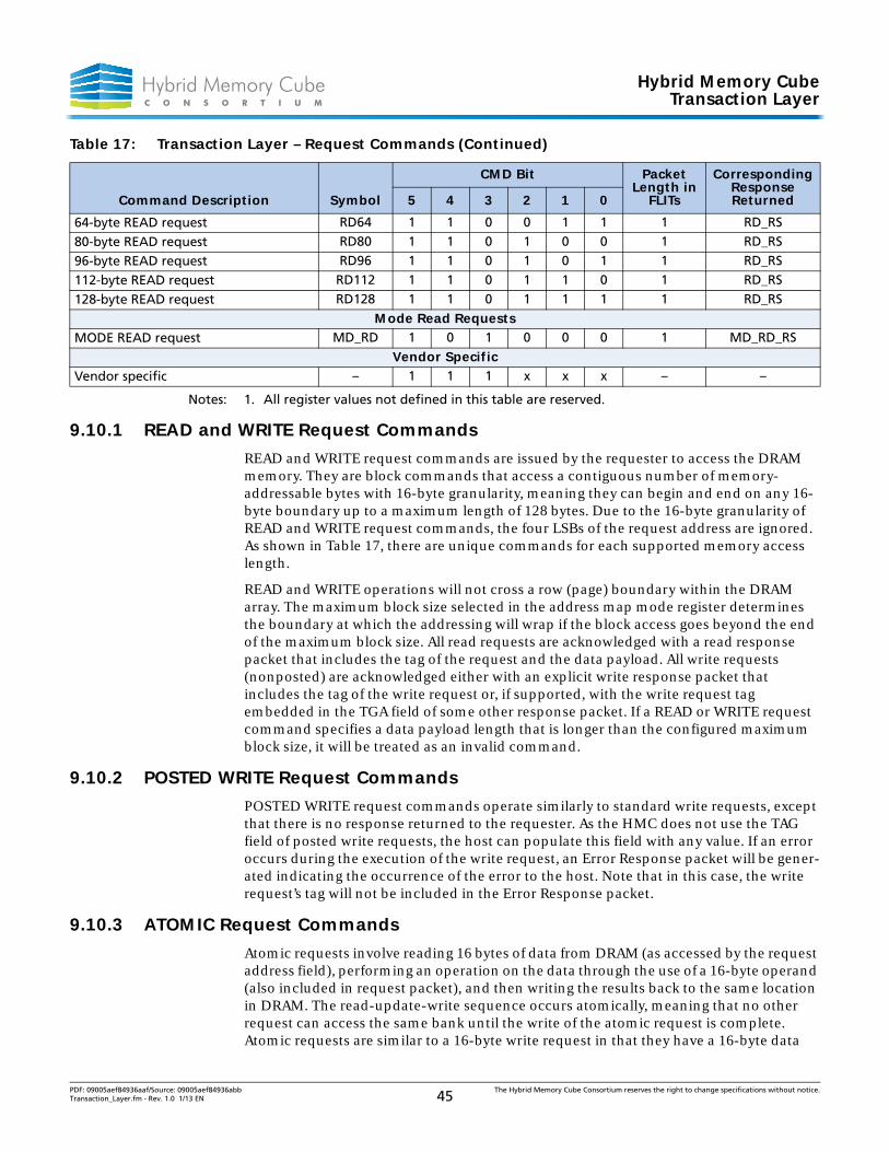
Hybrid Memory CubeTransaction Layer
Notes: 1. All register values not defined in this table are reserved.
9.10.1 READ and WRITE Request Commands
READ and WRITE request commands are issued by the requester to access the DRAM memory. They are block commands that access a contiguous number of memory-addressable bytes with 16-byte granularity, meaning they can begin and end on any 16-byte boundary up to a maximum length of 128 bytes. Due to the 16-byte granularity of READ and WRITE request commands, the four LSBs of the request address are ignored. As shown in Table 17, there are unique commands for each supported memory access length.
READ and WRITE operations will not cross a row (page) boundary within the DRAM array. The maximum block size selected in the address map mode register determines the boundary at which the addressing will wrap if the block access goes beyond the end of the maximum block size. All read requests are acknowledged with a read response packet that includes the tag of the request and the data payload. All write requests (nonposted) are acknowledged either with an explicit write response packet that includes the tag of the write request or, if supported, with the write request tag embedded in the TGA field of some other response packet. If a READ or WRITE request command specifies a data payload length that is longer than the configured maximum block size, it will be treated as an invalid command.
9.10.2 POSTED WRITE Request Commands
POSTED WRITE request commands operate similarly to standard write requests, except that there is no response returned to the requester. As the HMC does not use the TAG field of posted write requests, the host can populate this field with any value. If an error occurs during the execution of the write request, an Error Response packet will be gener-ated indicating the occurrence of the error to the host. Note that in this case, the write request’s tag will not be included in the Error Response packet.
9.10.3 ATOMIC Request Commands
Atomic requests involve reading 16 bytes of data from DRAM (as accessed by the request address field), performing an operation on the data through the use of a 16-byte operand (also included in request packet), and then writing the results back to the same location in DRAM. The read-update-write sequence occurs atomically, meaning that no other request can access the same bank until the write of the atomic request is complete. Atomic requests are similar to a 16-byte write request in that they have a 16-byte data
64-byte READ request RD64 1 1 0 0 1 1 1 RD_RS
80-byte READ request RD80 1 1 0 1 0 0 1 RD_RS
96-byte READ request RD96 1 1 0 1 0 1 1 RD_RS
112-byte READ request RD112 1 1 0 1 1 0 1 RD_RS
128-byte READ request RD128 1 1 0 1 1 1 1 RD_RS
Mode Read RequestsMODE READ request MD_RD 1 0 1 0 0 0 1 MD_RD_RS
Vendor SpecificVendor specific – 1 1 1 x x x – –
Table 17: Transaction Layer – Request Commands (Continued)
Command Description Symbol
CMD Bit Packet Length in
FLITs
Corresponding Response Returned5 4 3 2 1 0
PDF: 09005aef84936aaf/Source: 09005aef84936abb The Hybrid Memory Cube Consortium reserves the right to change specifications without notice.Transaction_Layer.fm - Rev. 1.0 1/13 EN 45
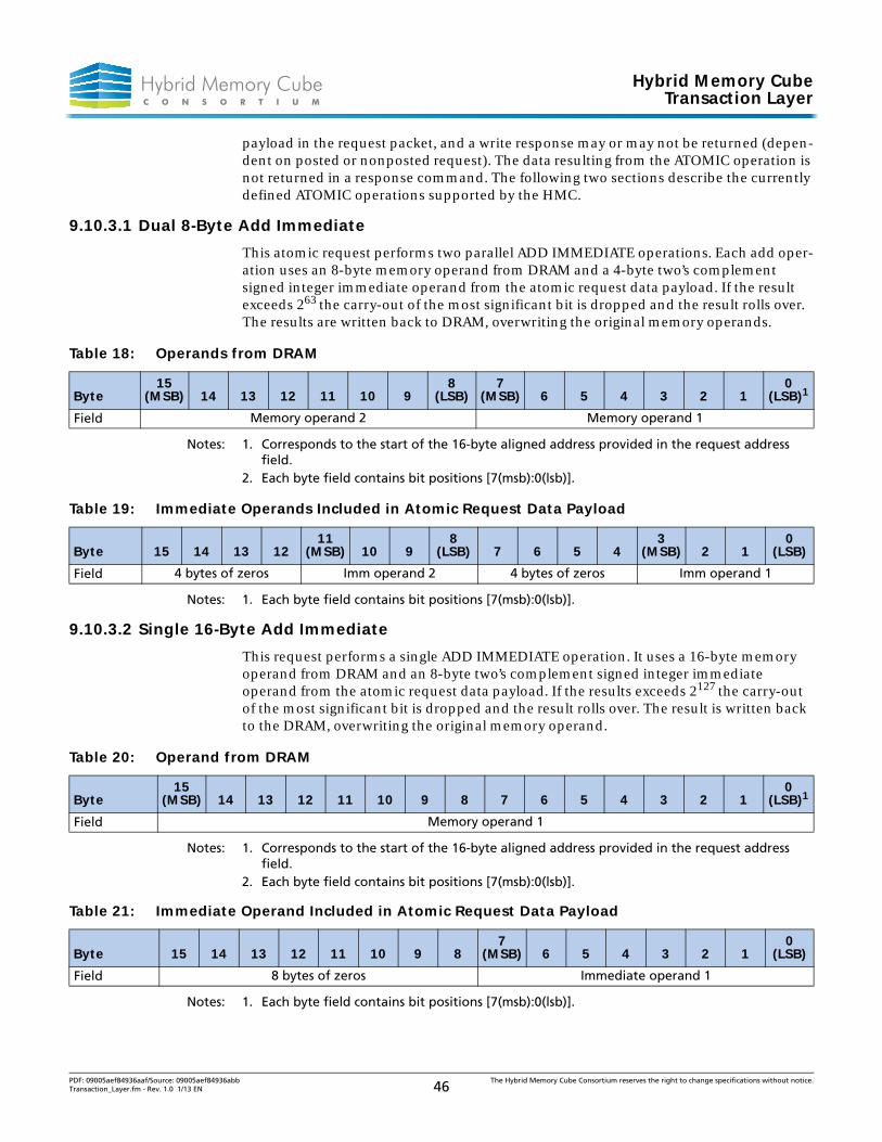
Hybrid Memory CubeTransaction Layer
payload in the request packet, and a write response may or may not be returned (depen-dent on posted or nonposted request). The data resulting from the ATOMIC operation is not returned in a response command. The following two sections describe the currently defined ATOMIC operations supported by the HMC.
9.10.3.1 Dual 8-Byte Add Immediate
This atomic request performs two parallel ADD IMMEDIATE operations. Each add oper-ation uses an 8-byte memory operand from DRAM and a 4-byte two’s complement signed integer immediate operand from the atomic request data payload. If the result exceeds 263 the carry-out of the most significant bit is dropped and the result rolls over. The results are written back to DRAM, overwriting the original memory operands.
Notes: 1. Corresponds to the start of the 16-byte aligned address provided in the request address field.
2. Each byte field contains bit positions [7(msb):0(lsb)].
Notes: 1. Each byte field contains bit positions [7(msb):0(lsb)].
9.10.3.2 Single 16-Byte Add Immediate
This request performs a single ADD IMMEDIATE operation. It uses a 16-byte memory operand from DRAM and an 8-byte two’s complement signed integer immediate operand from the atomic request data payload. If the results exceeds 2127 the carry-out of the most significant bit is dropped and the result rolls over. The result is written back to the DRAM, overwriting the original memory operand.
Notes: 1. Corresponds to the start of the 16-byte aligned address provided in the request address field.
2. Each byte field contains bit positions [7(msb):0(lsb)].
Notes: 1. Each byte field contains bit positions [7(msb):0(lsb)].
Table 18: Operands from DRAM
Byte15
(MSB) 14 13 12 11 10 98
(LSB)7
(MSB) 6 5 4 3 2 10
(LSB)1
Field Memory operand 2 Memory operand 1
Table 19: Immediate Operands Included in Atomic Request Data Payload
Byte 15 14 13 1211
(MSB) 10 98
(LSB) 7 6 5 43
(MSB) 2 10
(LSB)
Field 4 bytes of zeros Imm operand 2 4 bytes of zeros Imm operand 1
Table 20: Operand from DRAM
Byte15
(MSB) 14 13 12 11 10 9 8 7 6 5 4 3 2 10
(LSB)1
Field Memory operand 1
Table 21: Immediate Operand Included in Atomic Request Data Payload
Byte 15 14 13 12 11 10 9 87
(MSB) 6 5 4 3 2 10
(LSB)
Field 8 bytes of zeros Immediate operand 1
PDF: 09005aef84936aaf/Source: 09005aef84936abb The Hybrid Memory Cube Consortium reserves the right to change specifications without notice.Transaction_Layer.fm - Rev. 1.0 1/13 EN 46
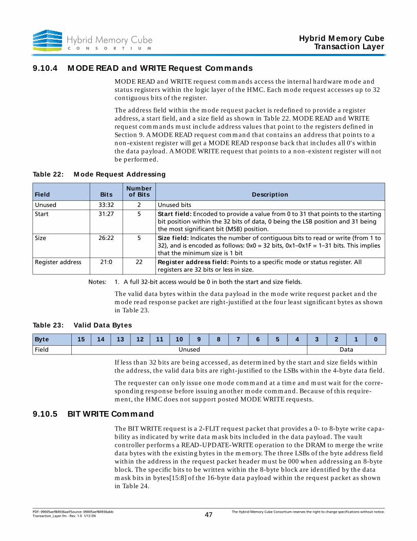
Hybrid Memory CubeTransaction Layer
9.10.4 MODE READ and WRITE Request Commands
MODE READ and WRITE request commands access the internal hardware mode and status registers within the logic layer of the HMC. Each mode request accesses up to 32 contiguous bits of the register.
The address field within the mode request packet is redefined to provide a register address, a start field, and a size field as shown in Table 22. MODE READ and WRITE request commands must include address values that point to the registers defined in Section 9. A MODE READ request command that contains an address that points to a non-existent register will get a MODE READ response back that includes all 0's within the data payload. A MODE WRITE request that points to a non-existent register will not be performed.
Notes: 1. A full 32-bit access would be 0 in both the start and size fields.
The valid data bytes within the data payload in the mode write request packet and the mode read response packet are right-justified at the four least significant bytes as shown in Table 23.
If less than 32 bits are being accessed, as determined by the start and size fields within the address, the valid data bits are right-justified to the LSBs within the 4-byte data field.
The requester can only issue one mode command at a time and must wait for the corre-sponding response before issuing another mode command. Because of this require-ment, the HMC does not support posted MODE WRITE requests.
9.10.5 BIT WRITE Command
The BIT WRITE request is a 2-FLIT request packet that provides a 0- to 8-byte write capa-bility as indicated by write data mask bits included in the data payload. The vault controller performs a READ-UPDATE-WRITE operation to the DRAM to merge the write data bytes with the existing bytes in the memory. The three LSBs of the byte address field within the address in the request packet header must be 000 when addressing an 8-byte block. The specific bits to be written within the 8-byte block are identified by the data mask bits in bytes[15:8] of the 16-byte data payload within the request packet as shown in Table 24.
Table 22: Mode Request Addressing
Field BitsNumber of Bits Description
Unused 33:32 2 Unused bitsStart 31:27 5 Start field: Encoded to provide a value from 0 to 31 that points to the starting
bit position within the 32 bits of data, 0 being the LSB position and 31 being the most significant bit (MSB) position.
Size 26:22 5 Size field: Indicates the number of contiguous bits to read or write (from 1 to 32), and is encoded as follows: 0x0 = 32 bits, 0x1–0x1F = 1–31 bits. This implies that the minimum size is 1 bit
Register address 21:0 22 Register address field: Points to a specific mode or status register. All registers are 32 bits or less in size.
Table 23: Valid Data Bytes
Byte 15 14 13 12 11 10 9 8 7 6 5 4 3 2 1 0
Field Unused Data
PDF: 09005aef84936aaf/Source: 09005aef84936abb The Hybrid Memory Cube Consortium reserves the right to change specifications without notice.Transaction_Layer.fm - Rev. 1.0 1/13 EN 47
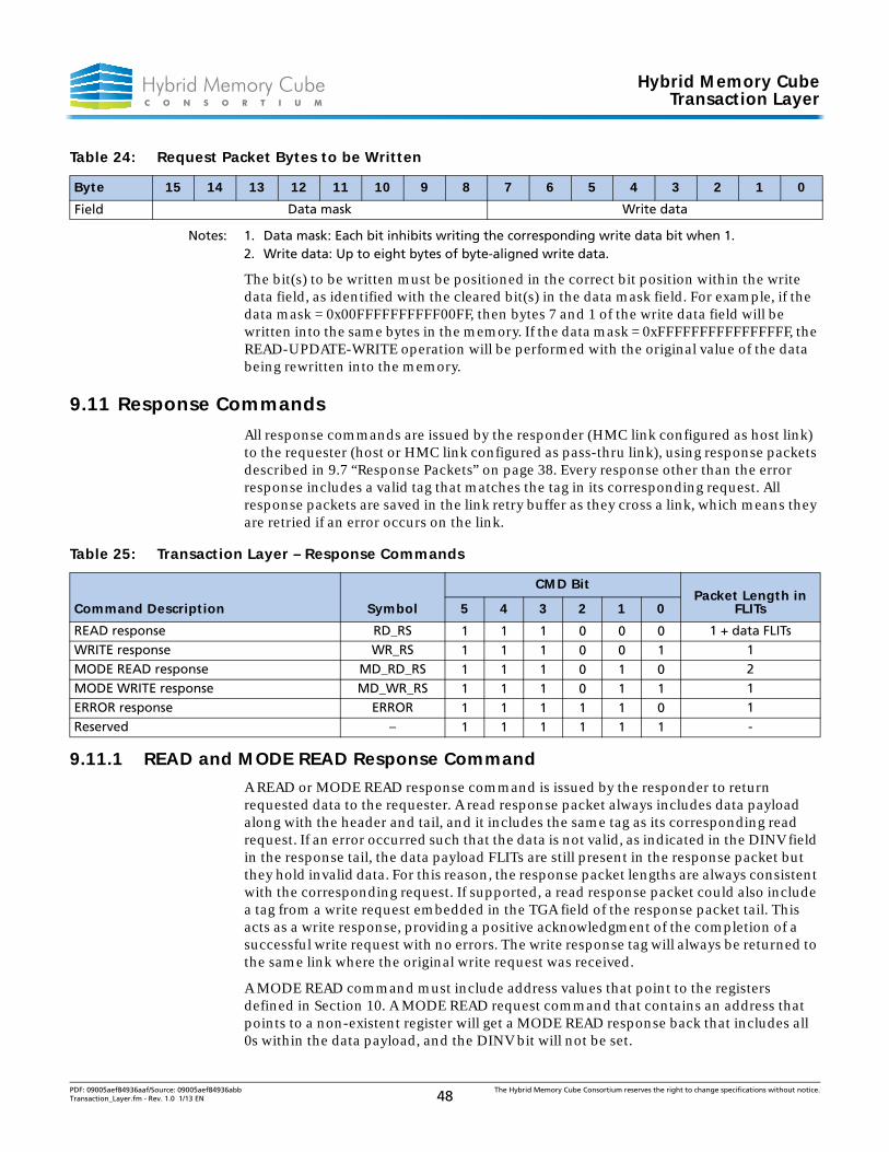
Hybrid Memory CubeTransaction Layer
Notes: 1. Data mask: Each bit inhibits writing the corresponding write data bit when 1. 2. Write data: Up to eight bytes of byte-aligned write data.
The bit(s) to be written must be positioned in the correct bit position within the write data field, as identified with the cleared bit(s) in the data mask field. For example, if the data mask = 0x00FFFFFFFFFF00FF, then bytes 7 and 1 of the write data field will be written into the same bytes in the memory. If the data mask = 0xFFFFFFFFFFFFFFFF, the READ-UPDATE-WRITE operation will be performed with the original value of the data being rewritten into the memory.
9.11 Response Commands
All response commands are issued by the responder (HMC link configured as host link) to the requester (host or HMC link configured as pass-thru link), using response packets described in 9.7 “Response Packets” on page 38. Every response other than the error response includes a valid tag that matches the tag in its corresponding request. All response packets are saved in the link retry buffer as they cross a link, which means they are retried if an error occurs on the link.
9.11.1 READ and MODE READ Response Command
A READ or MODE READ response command is issued by the responder to return requested data to the requester. A read response packet always includes data payload along with the header and tail, and it includes the same tag as its corresponding read request. If an error occurred such that the data is not valid, as indicated in the DINV field in the response tail, the data payload FLITs are still present in the response packet but they hold invalid data. For this reason, the response packet lengths are always consistent with the corresponding request. If supported, a read response packet could also include a tag from a write request embedded in the TGA field of the response packet tail. This acts as a write response, providing a positive acknowledgment of the completion of a successful write request with no errors. The write response tag will always be returned to the same link where the original write request was received.
A MODE READ command must include address values that point to the registers defined in Section 10. A MODE READ request command that contains an address that points to a non-existent register will get a MODE READ response back that includes all 0s within the data payload, and the DINV bit will not be set.
Table 24: Request Packet Bytes to be Written
Byte 15 14 13 12 11 10 9 8 7 6 5 4 3 2 1 0
Field Data mask Write data
Table 25: Transaction Layer – Response Commands
Command Description Symbol
CMD BitPacket Length in
FLITs5 4 3 2 1 0
READ response RD_RS 1 1 1 0 0 0 1 + data FLITsWRITE response WR_RS 1 1 1 0 0 1 1MODE READ response MD_RD_RS 1 1 1 0 1 0 2MODE WRITE response MD_WR_RS 1 1 1 0 1 1 1ERROR response ERROR 1 1 1 1 1 0 1Reserved – 1 1 1 1 1 1 -
PDF: 09005aef84936aaf/Source: 09005aef84936abb The Hybrid Memory Cube Consortium reserves the right to change specifications without notice.Transaction_Layer.fm - Rev. 1.0 1/13 EN 48
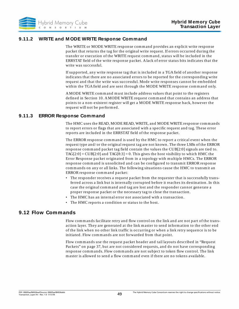
Hybrid Memory CubeTransaction Layer
9.11.2 WRITE and MODE WRITE Response Command
The WRITE or MODE WRITE response command provides an explicit write response packet that returns the tag for the original write request. If errors occurred during the transfer or execution of the WRITE request command, status will be included in the ERRSTAT field of the write response packet. A lack of error status bits indicates that the write was successful.
If supported, any write response tag that is included in a TGA field of another response indicates that there are no associated errors to be reported for the corresponding write request and that the write was successful. Mode write responses cannot be embedded within the TGA field and are sent through the MODE WRITE response command only.
A MODE WRITE command must include address values that point to the registers defined in Section 10. A MODE WRITE request command that contains an address that points to a non-existent register will get a MODE WRITE response back, however the request will not be performed.
9.11.3 ERROR Response Command
The HMC uses the READ, MODE READ, WRITE, and MODE WRITE response commands to report errors or flags that are associated with a specific request and tag. These error reports are included in the ERRSTAT field of the response packet.
The ERROR response command is used by the HMC to report a critical event when the request type and/or the original request tag are not known. The three LSBs of the ERROR response command packet tag field contain the values the CUB[2:0] signals are tied to. TAG[2:0] = CUB[2:0] and TAG[8:3] = 0. This gives the host visibility to which HMC the Error Response packet originated from in a topology with multiple HMCs. The ERROR response command is unsolicited and can be configured to transmit ERROR response commands on any or all links. The following situations cause the HMC to transmit an ERROR response command packet:• The responder receives a request packet from the requester that is successfully trans-
ferred across a link but is internally corrupted before it reaches its destination. In this case the original command and tag are lost and the responder cannot generate a proper response packet or the necessary tag to close the transaction.
• The HMC has an internal error not associated with a transaction. • The HMC reports a condition or status to the host.
9.12 Flow Commands
Flow commands facilitate retry and flow control on the link and are not part of the trans-action layer. They are generated at the link master to send information to the other end of the link when no other link traffic is occurring or when a link retry sequence is to be initiated. Flow commands are not forwarded from that point.
Flow commands use the request packet header and tail layouts described in “Request Packets” on page 37, but are not considered requests, and do not have corresponding response commands. Flow commands are not subject to token flow control. The link master is allowed to send a flow command even if there are no tokens available.
PDF: 09005aef84936aaf/Source: 09005aef84936abb The Hybrid Memory Cube Consortium reserves the right to change specifications without notice.Transaction_Layer.fm - Rev. 1.0 1/13 EN 49
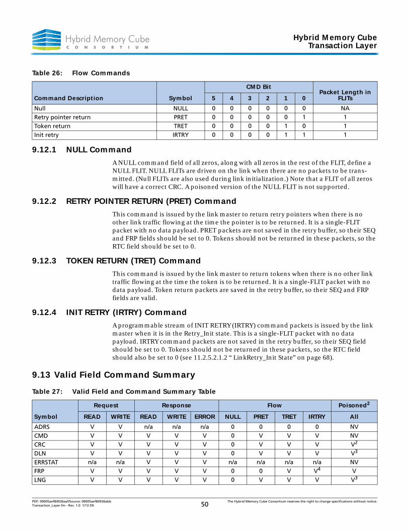
Hybrid Memory CubeTransaction Layer
9.12.1 NULL Command
A NULL command field of all zeros, along with all zeros in the rest of the FLIT, define a NULL FLIT. NULL FLITs are driven on the link when there are no packets to be trans-mitted. (Null FLITs are also used during link initialization.) Note that a FLIT of all zeros will have a correct CRC. A poisoned version of the NULL FLIT is not supported.
9.12.2 RETRY POINTER RETURN (PRET) Command
This command is issued by the link master to return retry pointers when there is no other link traffic flowing at the time the pointer is to be returned. It is a single-FLIT packet with no data payload. PRET packets are not saved in the retry buffer, so their SEQ and FRP fields should be set to 0. Tokens should not be returned in these packets, so the RTC field should be set to 0.
9.12.3 TOKEN RETURN (TRET) Command
This command is issued by the link master to return tokens when there is no other link traffic flowing at the time the token is to be returned. It is a single-FLIT packet with no data payload. Token return packets are saved in the retry buffer, so their SEQ and FRP fields are valid.
9.12.4 INIT RETRY (IRTRY) Command
A programmable stream of INIT RETRY (IRTRY) command packets is issued by the link master when it is in the Retry_Init state. This is a single-FLIT packet with no data payload. IRTRY command packets are not saved in the retry buffer, so their SEQ field should be set to 0. Tokens should not be returned in these packets, so the RTC field should also be set to 0 (see 11.2.5.2.1.2 “ LinkRetry_Init State” on page 68).
9.13 Valid Field Command Summary
Table 26: Flow Commands
Command Description Symbol
CMD BitPacket Length in
FLITs5 4 3 2 1 0
Null NULL 0 0 0 0 0 0 NA
Retry pointer return PRET 0 0 0 0 0 1 1
Token return TRET 0 0 0 0 1 0 1
Init retry IRTRY 0 0 0 0 1 1 1
Table 27: Valid Field and Command Summary Table
Symbol
Request Response Flow Poisoned2
READ WRITE READ WRITE ERROR NULL PRET TRET IRTRY All
ADRS V V n/a n/a n/a 0 0 0 0 NV
CMD V V V V V 0 V V V NV
CRC V V V V V 0 V V V V2
DLN V V V V V 0 V V V V3
ERRSTAT n/a n/a V V V n/a n/a n/a n/a NV
FRP V V V V V 0 0 V V4 V
LNG V V V V V 0 V V V V3
PDF: 09005aef84936aaf/Source: 09005aef84936abb The Hybrid Memory Cube Consortium reserves the right to change specifications without notice.Transaction_Layer.fm - Rev. 1.0 1/13 EN 50
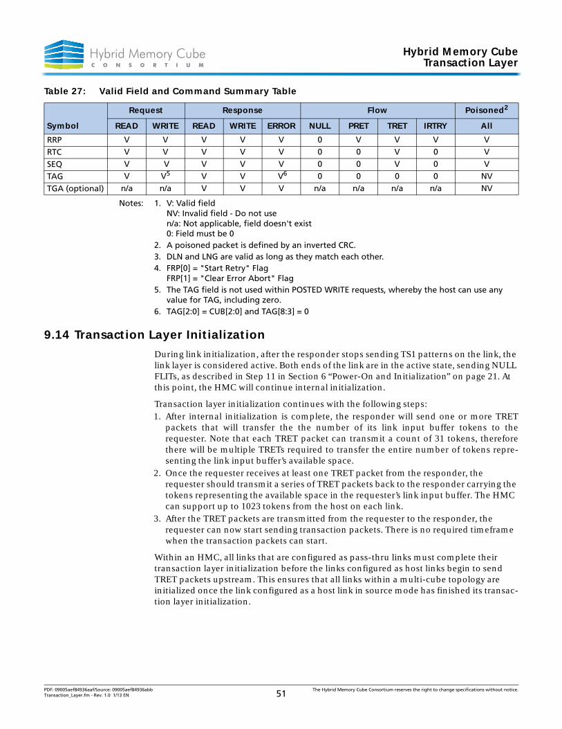
Hybrid Memory CubeTransaction Layer
Notes: 1. V: Valid fieldNV: Invalid field - Do not usen/a: Not applicable, field doesn't exist0: Field must be 0
2. A poisoned packet is defined by an inverted CRC.3. DLN and LNG are valid as long as they match each other.4. FRP[0] = "Start Retry" Flag
FRP[1] = "Clear Error Abort" Flag5. The TAG field is not used within POSTED WRITE requests, whereby the host can use any
value for TAG, including zero.6. TAG[2:0] = CUB[2:0] and TAG[8:3] = 0
9.14 Transaction Layer Initialization
During link initialization, after the responder stops sending TS1 patterns on the link, the link layer is considered active. Both ends of the link are in the active state, sending NULL FLITs, as described in Step 11 in Section 6 “Power-On and Initialization” on page 21. At this point, the HMC will continue internal initialization.
Transaction layer initialization continues with the following steps:1. After internal initialization is complete, the responder will send one or more TRET
packets that will transfer the the number of its link input buffer tokens to therequester. Note that each TRET packet can transmit a count of 31 tokens, thereforethere will be multiple TRETs required to transfer the entire number of tokens repre-senting the link input buffer’s available space.
2. Once the requester receives at least one TRET packet from the responder, the requester should transmit a series of TRET packets back to the responder carrying the tokens representing the available space in the requester’s link input buffer. The HMC can support up to 1023 tokens from the host on each link.
3. After the TRET packets are transmitted from the requester to the responder, the requester can now start sending transaction packets. There is no required timeframe when the transaction packets can start.
Within an HMC, all links that are configured as pass-thru links must complete their transaction layer initialization before the links configured as host links begin to send TRET packets upstream. This ensures that all links within a multi-cube topology are initialized once the link configured as a host link in source mode has finished its transac-tion layer initialization.
RRP V V V V V 0 V V V V
RTC V V V V V 0 0 V 0 V
SEQ V V V V V 0 0 V 0 V
TAG V V5 V V V6 0 0 0 0 NV
TGA (optional) n/a n/a V V V n/a n/a n/a n/a NV
Table 27: Valid Field and Command Summary Table
Symbol
Request Response Flow Poisoned2
READ WRITE READ WRITE ERROR NULL PRET TRET IRTRY All
PDF: 09005aef84936aaf/Source: 09005aef84936abb The Hybrid Memory Cube Consortium reserves the right to change specifications without notice.Transaction_Layer.fm - Rev. 1.0 1/13 EN 51
Hybrid Memory CubeConfiguration and Status Registers
10 Configuration and Status RegistersThere are two methods supported for accessing the HMC configuration and status regis-ters:
Direct access: This type of access uses the in-band MODE WRITE and MODE READ request commands or the sideband (JTAG/I2C) to directly read or write the configura-tion and status registers. Tables 33–41 contain the configuration and status registers accessible by direct access that are supported by this specification. All other register functions are considered vendor specific.
Indirect access through the external data interface (ERI): This type of access utilizes four External Data Registers (see Tables 28–31) and an External Request Register (see Table 32) to indirectly access the HMC configuration and status registers. The external data and request registers are accessible through MODE WRITE and MODE READ requests or sideband (JTAG/I2C). Specific configuration and status registers accessible through the ERI are not contained within this specification, only the framework to enable this type of register access. See Figure 16 on page 53 for the steps required to access the configuration and status registers through the ERI.
PDF: 09005aef84936aaf/Source: 09005aef84936abb The Hybrid Memory Cube Consortium reserves the right to change specifications without notice.Transaction_Layer.fm - Rev. 1.0 1/13 EN 52
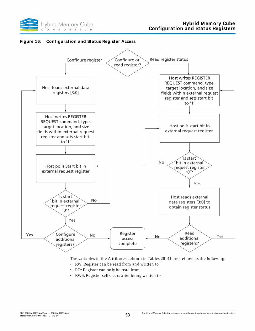
Hybrid Memory CubeConfiguration and Status Registers
Figure 16: Configuration and Status Register Access
The variables in the Attributes column in Tables 28–41 are defined as the following:• RW: Register can be read from and written to• RO: Register can only be read from• RWS: Register self clears after being written to
Host loads external dataregisters [3:0]
Read register statusConfigure register
Host writes REGISTERREQUEST command, type,target location, and size
fields within external requestregister and sets start bit
to ‘1’
Host polls Start bit inexternal request register
Is startbit in external
request register‘0’?
Configureadditionalregisters?
Registeraccess
complete
No
No
Yes
Yes
Host writes REGISTERREQUEST command, type,target location, and size
fields within external requestregister and sets start bit
to ‘1’
Host polls start bit inexternal request register
Is startbit in external
request register‘0’?
Readadditionalregisters?
Yes
No
Configure or read register?
Host reads externaldata registers [3:0] toobtain register status
YesNo
PDF: 09005aef84936aaf/Source: 09005aef84936abb The Hybrid Memory Cube Consortium reserves the right to change specifications without notice.Transaction_Layer.fm - Rev. 1.0 1/13 EN 53
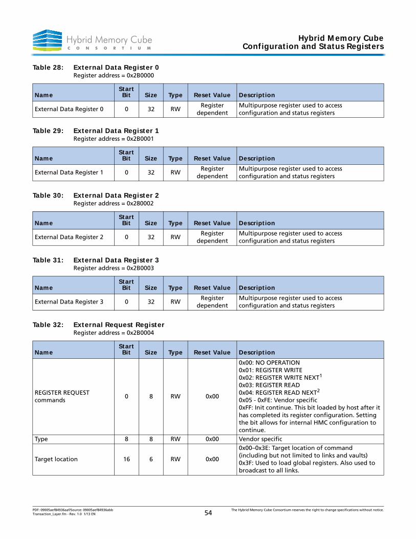
Hybrid Memory CubeConfiguration and Status Registers
Table 28: External Data Register 0Register address = 0x2B0000
NameStart Bit Size Type Reset Value Description
External Data Register 0 0 32 RWRegister
dependentMultipurpose register used to access configuration and status registers
Table 29: External Data Register 1Register address = 0x2B0001
NameStart Bit Size Type Reset Value Description
External Data Register 1 0 32 RWRegister
dependentMultipurpose register used to access configuration and status registers
Table 30: External Data Register 2Register address = 0x280002
NameStart Bit Size Type Reset Value Description
External Data Register 2 0 32 RWRegister
dependentMultipurpose register used to access configuration and status registers
Table 31: External Data Register 3Register address = 0x2B0003
NameStart Bit Size Type Reset Value Description
External Data Register 3 0 32 RWRegister
dependentMultipurpose register used to access configuration and status registers
Table 32: External Request RegisterRegister address = 0x2B0004
NameStart Bit Size Type Reset Value Description
REGISTER REQUEST commands
0 8 RW 0x00
0x00: NO OPERATION0x01: REGISTER WRITE0x02: REGISTER WRITE NEXT1 0x03: REGISTER READ0x04: REGISTER READ NEXT2
0x05 - 0xFE: Vendor specific0xFF: Init continue. This bit loaded by host after it has completed its register configuration. Setting the bit allows for internal HMC configuration to continue.
Type 8 8 RW 0x00 Vendor specific
Target location 16 6 RW 0x00
0x00–0x3E: Target location of command (including but not limited to links and vaults)0x3F: Used to load global registers. Also used to broadcast to all links.
PDF: 09005aef84936aaf/Source: 09005aef84936abb The Hybrid Memory Cube Consortium reserves the right to change specifications without notice.Transaction_Layer.fm - Rev. 1.0 1/13 EN 54
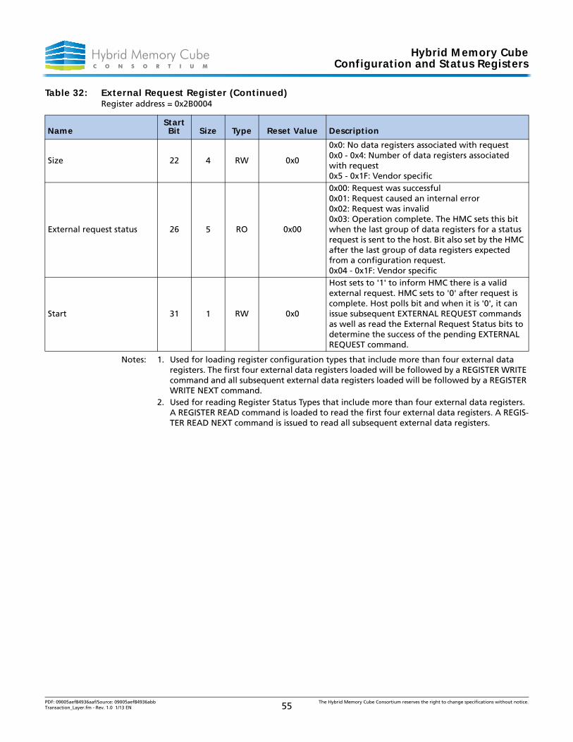
Hybrid Memory CubeConfiguration and Status Registers
Notes: 1. Used for loading register configuration types that include more than four external data registers. The first four external data registers loaded will be followed by a REGISTER WRITE command and all subsequent external data registers loaded will be followed by a REGISTER WRITE NEXT command.
2. Used for reading Register Status Types that include more than four external data registers. A REGISTER READ command is loaded to read the first four external data registers. A REGIS-TER READ NEXT command is issued to read all subsequent external data registers.
Size 22 4 RW 0x0
0x0: No data registers associated with request0x0 - 0x4: Number of data registers associated with request0x5 - 0x1F: Vendor specific
External request status 26 5 RO 0x00
0x00: Request was successful0x01: Request caused an internal error0x02: Request was invalid0x03: Operation complete. The HMC sets this bit when the last group of data registers for a status request is sent to the host. Bit also set by the HMC after the last group of data registers expected from a configuration request.0x04 - 0x1F: Vendor specific
Start 31 1 RW 0x0
Host sets to '1' to inform HMC there is a valid external request. HMC sets to '0' after request is complete. Host polls bit and when it is '0', it can issue subsequent EXTERNAL REQUEST commands as well as read the External Request Status bits to determine the success of the pending EXTERNAL REQUEST command.
Table 32: External Request Register (Continued)Register address = 0x2B0004
NameStart Bit Size Type Reset Value Description
PDF: 09005aef84936aaf/Source: 09005aef84936abb The Hybrid Memory Cube Consortium reserves the right to change specifications without notice.Transaction_Layer.fm - Rev. 1.0 1/13 EN 55
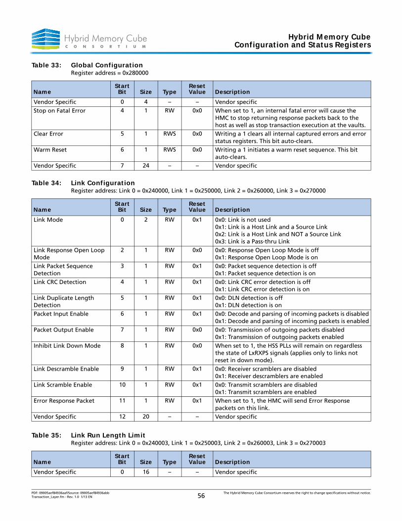
Hybrid Memory CubeConfiguration and Status Registers
Table 33: Global ConfigurationRegister address = 0x280000
NameStart Bit Size Type
ResetValue Description
Vendor Specific 0 4 – – Vendor specificStop on Fatal Error 4 1 RW 0x0 When set to 1, an internal fatal error will cause the
HMC to stop returning response packets back to the host as well as stop transaction execution at the vaults.
Clear Error 5 1 RWS 0x0 Writing a 1 clears all internal captured errors and error status registers. This bit auto-clears.
Warm Reset 6 1 RWS 0x0 Writing a 1 initiates a warm reset sequence. This bit auto-clears.
Vendor Specific 7 24 – – Vendor specific
Table 34: Link ConfigurationRegister address: Link 0 = 0x240000, Link 1 = 0x250000, Link 2 = 0x260000, Link 3 = 0x270000
NameStart Bit Size Type
ResetValue Description
Link Mode 0 2 RW 0x1 0x0: Link is not used0x1: Link is a Host Link and a Source Link0x2: Link is a Host Link and NOT a Source Link0x3: Link is a Pass-thru Link
Link Response Open Loop Mode
2 1 RW 0x0 0x0: Response Open Loop Mode is off0x1: Response Open Loop Mode is on
Link Packet Sequence Detection
3 1 RW 0x1 0x0: Packet sequence detection is off0x1: Packet sequence detection is on
Link CRC Detection 4 1 RW 0x1 0x0: Link CRC error detection is off0x1: Link CRC error detection is on
Link Duplicate Length Detection
5 1 RW 0x1 0x0: DLN detection is off0x1: DLN detection is on
Packet Input Enable 6 1 RW 0x1 0x0: Decode and parsing of incoming packets is disabled0x1: Decode and parsing of incoming packets is enabled
Packet Output Enable 7 1 RW 0x0 0x0: Transmission of outgoing packets disabled0x1: Transmission of outgoing packets enabled
Inhibit Link Down Mode 8 1 RW 0x0 When set to 1, the HSS PLLs will remain on regardless the state of LxRXPS signals (applies only to links not reset in down mode).
Link Descramble Enable 9 1 RW 0x1 0x0: Receiver scramblers are disabled0x1: Receiver descramblers are enabled
Link Scramble Enable 10 1 RW 0x1 0x0: Transmit scramblers are disabled0x1: Transmit scramblers are enabled
Error Response Packet 11 1 RW 0x1 When set to 1, the HMC will send Error Response packets on this link.
Vendor Specific 12 20 – – Vendor specific
Table 35: Link Run Length LimitRegister address: Link 0 = 0x240003, Link 1 = 0x250003, Link 2 = 0x260003, Link 3 = 0x270003
NameStart Bit Size Type
ResetValue Description
Vendor Specific 0 16 – – Vendor specific
PDF: 09005aef84936aaf/Source: 09005aef84936abb The Hybrid Memory Cube Consortium reserves the right to change specifications without notice.Transaction_Layer.fm - Rev. 1.0 1/13 EN 56
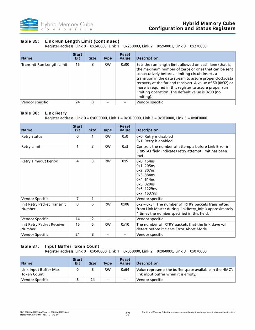
Hybrid Memory CubeConfiguration and Status Registers
Transmit Run Length Limit 16 8 RW 0x00 Sets the run length limit allowed on each lane (that is, the maximum number of zeros or ones that can be sent consecutively before a limiting circuit inserts a transition in the data stream to assure proper clock/data recovery at the far end receiver). A value of 50 (0x32) or more is required in this register to assure proper run limiting operation. The default value is 0x00 (no limiting).
Vendor specific 24 8 – – Vendor specific
Table 36: Link RetryRegister address: Link 0 = 0x0C0000, Link 1 = 0x0D0000, Link 2 = 0x0E0000, Link 3 = 0x0F0000
NameStart Bit Size Type
ResetValue Description
Retry Status 0 1 RW 0x0 0x0: Retry is disabled0x1: Retry is enabled
Retry Limit 1 3 RW 0x3 Controls the number of attempts before Link Error in ERRSTAT field indicates retry attempt limit has been met.
Retry Timeout Period 4 3 RW 0x5 0x0: 154ns0x1: 205ns0x2: 307ns0x3: 384ns0x4: 614ns0x5: 820ns0x6: 1229ns0x7: 1637ns
Vendor Specific 7 1 – – Vendor specificInit Retry Packet Transmit Number
8 6 RW 0x08 0x2 – 0x3F: The number of IRTRY packets transmitted from Link Master during LinkRetry_Init is approximately 4 times the number specified in this field.
Vendor Specific 14 2 – – Vendor specificInit Retry Packet Receive Number
16 6 RW 0x10 The number of IRTRY packets that the link slave will detect before it clears Error Abort Mode.
Vendor Specific 24 8 – – Vendor specific
Table 37: Input Buffer Token CountRegister address: Link 0 = 0x040000, Link 1 = 0x050000, Link 2 = 0x060000, Link 3 = 0x070000
NameStart Bit Size Type
ResetValue Description
Link Input Buffer Max Token Count
0 8 RW 0x64 Value represents the buffer space available in the HMC’s link input buffer when it is empty.
Vendor Specific 8 24 – – Vendor specific
Table 35: Link Run Length Limit (Continued)Register address: Link 0 = 0x240003, Link 1 = 0x250003, Link 2 = 0x260003, Link 3 = 0x270003
NameStart Bit Size Type
ResetValue Description
PDF: 09005aef84936aaf/Source: 09005aef84936abb The Hybrid Memory Cube Consortium reserves the right to change specifications without notice.Transaction_Layer.fm - Rev. 1.0 1/13 EN 57
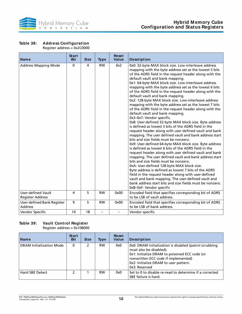
Hybrid Memory CubeConfiguration and Status Registers
Table 38: Address ConfigurationRegister address = 0x2C0000
NameStart Bit Size Type
ResetValue Description
Address Mapping Mode 0 4 RW 0x2 0x0: 32-byte MAX block size. Low-interleave address mapping with the byte address set as the lowest 5 bits of the ADRS field in the request header along with the default vault and bank mapping.0x1: 64-byte MAX block size. Low-interleave address mapping with the byte address set as the lowest 6 bits of the ADRS field in the request header along with the default vault and bank mapping.0x2: 128-byte MAX block size. Low-interleave address mapping with the byte address set as the lowest 7 bits of the ADRS field in the request header along with the default vault and bank mapping.0x3–0x7: Vendor specific.0x8: User-defined 32-byte MAX block size. Byte address is defined as lowest 5 bits of the ADRS field in the request header along with user defined vault and bank mapping. The user defined vault and bank address start bits and size fields must be nonzero.0x9: User-defined 64-byte MAX block size. Byte address is defined as lowest 6 bits of the ADRS field in the request header along with user defined vault and bank mapping. The user defined vault and bank address start bits and size fields must be nonzero.0xA: User-defined 128-byte MAX block size.Byte address is defined as lowest 7 bits of the ADRS field in the request header along with user-defined vault and bank mapping. The user-defined vault and bank address start bits and size fields must be nonzero.0xB–0xF: Vendor specific
User-defined Vault Register Address
4 5 RW 0x00 Encoded field that specifies corresponding bit of ADRS to be LSB of vault address.
User-defined Bank Register Address
9 5 RW 0x00 Encoded field that specifies corresponding bit of ADRS to be LSB of bank address.
Vendor Specific 14 18 – – Vendor specific
Table 39: Vault Control RegisterRegister address = 0x108000
NameStart Bit Size Type
ResetValue Description
DRAM Initialization Mode 0 2 RW 0x0 0x0: DRAM initialization is disabled (patrol scrubbing must also be disabled).0x1: Initialize DRAM to poisoned ECC code (or nonwritten ECC code if implemented)0x2: Initialize DRAM to user pattern.0x3: Reserved
Hard SBE Detect 2 1 RW 0x0 Set to 0 to disable re-read to determine if a corrected SBE failure is hard.
PDF: 09005aef84936aaf/Source: 09005aef84936abb The Hybrid Memory Cube Consortium reserves the right to change specifications without notice.Transaction_Layer.fm - Rev. 1.0 1/13 EN 58
Hybrid Memory CubeConfiguration and Status Registers
Demand Scrubbing 3 1 RW 0x1 Set to 0 to disable a scrub write to DRAM of corrected data when an SBE is detected on a transaction read request.
Patrol Scrubbing 4 1 RW 0x1 Set to 0 to disable a scrub write to DRAM of corrected data when an SBE is detected on a patrol read request.
Packet CRC Detection 5 1 RW 0x1 Set to 0 to disable the CRC check performed on incoming packets to the vault controllers. This allows the vault controller to execute request packets that have CRC errors.
Command/Address Retry Count
6 3 RW 0x1 When a command or address parity error is detected on DRAM commands, the vault controllers will perform up to the number of DRAM command retries specified in this field. If this field is 0, DRAM command retry is disabled.
Data ECC Correction 9 1 RW 0x1 Set to 1 to disable correction of a SBE if detected by the vault controller. Data from the DRAM will be returned unmodified in the response packet. Demand and patrol scrubbing are also disabled.
Vendor Specific 10 1 – – Vendor specificHard SBE Repair 11 1 RW 0x1 Set to 1 to invoke a dynamic repair operation when any
hard SBE is detected.Enable SBE Report 12 1 RW 0x1 Set to 1 to report any SBEs that occurred on a read
request within the ERRSTAT field of the read response.Vendor Specific 13 19 – – Vendor specific
Table 40: FeaturesRegister address = 0x2C0003
NameStart Bit Size Type
ResetValue Description
Cube Size 0 4 RO Product specific
0x00: 2GB0x01: 4GB0x02: 8GB0x03: 16GB0x4–0xF: Vendor specific
Number of Vaults 4 4 RO Product specific
0x0: 16 vaults0x1: 32 vaults0x2–0xF: Vendor specific
Number of Banks per Vault 8 4 RO Product specific
0x0: 8 banks0x1: 16 banks0x2–0xF: Vendor specific
PHY 12 4 RO Product specific
0x0: HMC-15G-SR0x1: HMC-10G-USR0x2–0xF: Vendor specific
Vendor Specific 16 16 – – Vendor specific
Table 39: Vault Control Register (Continued)Register address = 0x108000
NameStart Bit Size Type
ResetValue Description
PDF: 09005aef84936aaf/Source: 09005aef84936abb The Hybrid Memory Cube Consortium reserves the right to change specifications without notice.Transaction_Layer.fm - Rev. 1.0 1/13 EN 59

Hybrid Memory CubeConfiguration and Status Registers
Table 41: Revisions and Vendor IDRegister address = 0x2C0004
NameStart Bit Size Type
ResetValue Description
Vendor ID 0 8 RO Vendor specific
Vendor ID
Product Revision 8 8 RO Vendor specific
Product revision
Protocol Revision 16 8 RO Vendor specific
Protocol revision
PHY Revision 24 8 RO Vendor specific
PHY revision
PDF: 09005aef84936aaf/Source: 09005aef84936abb The Hybrid Memory Cube Consortium reserves the right to change specifications without notice.Transaction_Layer.fm - Rev. 1.0 1/13 EN 60
Hybrid Memory CubeLink Retry
11 Link Retry The link transmits data at a very high speed. The data transmission bit-failure rate requires a mechanism for correcting failures to increase system reliability and avail-ability. Link retry is a fault-tolerant feature that recovers the link when link errors occur. Link packet integrity is insured with a CRC code that resides in the tail of every packet. It covers all bits in the packet, including the header, any data payload, and the tail. CRC is generated at the link master before the packet bits are serialized and transmitted, and is checked at the link slave after the packet bits are received and deserialized. A mismatch indicates that some of the data within the packet has changed since the original CRC code was generated at the transmitting end of the link. An additional check is provided using an incrementing sequence number included in every packet. If the CRC check is successful upon receipt of the packet, the link slave will verify that the sequence number has a +1 value compared to the last successful packet received.
The link master saves a copy of each packet transmitted across the link. Each packet is held until an acknowledge occurs indicating that the packets have been received without errors. This acknowledgment comes from a retry pointer (included in every transmitted packet); it is returned to the link master embedded in packets traveling in the opposite direction on that link.
If the link slave detects a packet error, it enters error abort mode. This results in the failed packet being poisoned or dropped and all subsequent packets being dropped. Error Abort mode triggers the local link master to send a StartRetry flag back to the transmit-ting end using the other side of the link. The poisoned and dropped packets are then retransmitted by the link master during the retry sequence.
Figure 17 on page 62 illustrates an example implementation of the link retry blocks on both ends of a link. The forward retry pointer (FRP) and return retry pointer (RRP) extract and embed blocks are color coded to show the path the retry pointer takes for each link direction.
Note that the link is symmetrical and in the following discussions the requester can be either device A or device B. Similarly, the responder can be either device A or device B.
PDF: 09005aef84936aaf/Source: 09005aef84936abb The Hybrid Memory Cube Consortium reserves the right to change specifications without notice.Retry.fm - Rev. 1.0 1/13 EN 61
Hybrid Memory CubeLink Retry
Figure 17: Implementation Example of Link Retry Block Diagram
11.1 Retry Pointer Description
The retry pointer represents the packet's position in the retry buffer. The retry pointer transmitted with the packet points to the retry buffer location + 1 (to which the tail is being written). This is the starting address of the next packet to be transmitted.
There are two retry pointer versions: • The FRP as it travels in the forward direction on the link• The RRP, as the same retry pointer travels back on the other side of the link,
completing the round trip and eventually getting back to the retry buffer control logic in the link master
The FRP is sent with every packet that is part of the normal packet flow (other than IRTRY packets and PRET packets described later). Note that the retry buffer is addressed using FLIT addresses, and the retry pointer represents a FLIT position in the retry buffer. Even though a packet may be multiple FLITs, the retry pointer will always point to the header FLIT position of a packet.
Retrybuffer
Retrybuffer
FRPgen
FRPgen
OutputFIFO
OutputFIFO
InputFIFO
InputFIFO
TXSerDes
PhysicalTX
PhysicalRX
PhysicalRX
Retrycontrol
Retrycontrol
RRPembed
RRPembed
RRPextract
FRPextract
FRPextract
RRPextract
CRC, SEQCHK
CRC, SEQCHK
+
+
LM LS
LS LM
Greenpacket
FRP
RRP
Greenpacket
FRP
RRP
Bluepacket
RRP
FRP
Bluepacket
RRP
FRP
Device A Device B
Errorabortmode
Errorabortmode
StartRetry
StartRetry
PDF: 09005aef84936aaf/Source: 09005aef84936abb The Hybrid Memory Cube Consortium reserves the right to change specifications without notice.Retry.fm - Rev. 1.0 1/13 EN 62
Hybrid Memory CubeLink Retry
There are two pointer fields in the tail of a packet:• FRP field: This is the forward retry pointer as the packet is traveling in the forward
direction on the link. The FRP field is ignored in PRET packets and is redefined to contain two retry control flags in IRTRY packets.
• RRP field: This is the return retry pointer embedded in any packet traveling in the return direction of the link. If the return direction has no normal packet traffic, when an FRP is extracted in the local link slave and sent to the link master, a PRET packet is then created in the link master and the FRP is loaded into the RRP field. The RRP is not associated with the packet in which it is embedded, other than to “ride along” to get back to the other end of the link. The link is symmetrical in both directions, so RRPs are embedded in packet traffic moving in both directions. The RRP field of the packet is always valid, including IRTRY packets and PRET packets.
11.2 Link Master Retry Functions
Figure 18: Implementation Example of a Retry Buffer
In this implementation example, a retry buffer is used to save packets for potential retransmission if a link error occurs. The retry buffer relies on a write pointer and read pointer to track the status of the FLITs stored within it. The write pointer is advanced with valid outgoing FLITs as determined by the packet stream traveling out of the link master. As FLITs are written into the retry buffer, they are considered to be pending FLITs, because they may need to be re-transmitted if an error occurs. They remain pending FLITs until the read pointer is advanced past them, indicating that one or more returned retry pointers were received, representing a successful packet transmission.
The read pointer in this example is used to read data from the retry buffer during a retry sequence. If no errors occur, retry pointers are returned (RRPs) and used to advance the read pointer. As RRPs are received, the read pointer will rotate around the retry buffer address space, following the write pointer, and turn pending FLITs into retired FLITs.
RetiredFLITs
RetiredFLITs
PendingFLITs
n . . . .
8 7 6 5 4 3 2 1 0
Retry buffer read pointer
Retry buffer write pointer
FLIT in FLIT out
PDF: 09005aef84936aaf/Source: 09005aef84936abb The Hybrid Memory Cube Consortium reserves the right to change specifications without notice.Retry.fm - Rev. 1.0 1/13 EN 63
Hybrid Memory CubeLink Retry
Retired FLITs are unneeded residue FLITs that will eventually be overwritten by new pending FLITs as the write pointer advances and wraps around the retry buffer address space.
During a retry sequence, the read pointer is incremented until it equals the write pointer, indicating that all pending FLITs have been pulled out of the retry buffer and retrans-mitted across the link. All RRPs received during this period are saved in a read pointer hold register until all pending FLITs have been read out of the retry buffer. At the end of the LinkRetry_FLIT state (see 10.2.7.2.1.3 “LinkRetry_FLIT State”), as the retry control switches back to a flow of new packets, the latest value of the read pointer hold register is copied to the read pointer. This action may retire many of the pending FLITs. After the copy is made, any newly arrived RRPs are used to advance the read pointer directly, thus retiring more FLITs.
A threshold is implemented in this example to detect a near-full condition of the retry buffer. The near-full condition is detected by comparing the value of the write pointer to the read pointer. This threshold leaves enough room remaining in the retry buffer for the current packet in transmission to be completely saved in the retry buffer, without over-flow, when the near-full detection occurs. At this point, the link master will stop the packet flow to the link.
11.2.1 Forward Retry Pointer Generation
The link master generates the retry pointer and includes it in the FRP field in the tail of the packet being transmitted. The retry pointer is created by using the value where the tail FLIT of the packet is to be saved for potential retransmission, incrementing by +1, and loading it into the FRP field within the tail of the packet. This value points to the location where the header of the next packet to be transmitted will be saved. This FRP value must be included in the CRC generation, which is also loaded into the tail of the packet being transmitted. Note that the FRP field is valid for all packets that are saved for potential retransmission. All packets that are transmitted other than IRTRY, NULL, and PRET packets are saved until the success of their transmission has been acknowledged. If the original packet stream on the link included NULL FLITs between some of the packets, those NULL FLITs are not saved for potential retransmission. However, during a retry sequence, as the retried packet sequence is transmitted, NULL FLITs may be transmitted between packets.
11.2.2 Packet Sequence Number Generation
The link master generates a sequence number for every outgoing packet that is part of the normal packet flow and loads it into the SEQ field within the tail of the packet. The sequence number should be incremented by + 1 for every normal packet. The sequence number should increment by +1 for every packet that is saved for retransmission. It will not be generated for PRET or IRTRY packets, as these are not saved for retransmission. Any packets replayed during a retry sequence already have their sequence number embedded and are re-sent without updating the SEQ field.After the last retried packet is transmitted, the sequence number generator should increment for the next new packet that follows the retried packet stream. This accommodates a sequence checking across a retry sequence, verifying that all packets are sequential before, during, and after the retry sequence. The sequence number register in the link slave should be set to zero upon a cold or warm reset. The first packet sent from the link master after a cold or warm reset should contain a sequence number of 1.
PDF: 09005aef84936aaf/Source: 09005aef84936abb The Hybrid Memory Cube Consortium reserves the right to change specifications without notice.Retry.fm - Rev. 1.0 1/13 EN 64
Hybrid Memory CubeLink Retry
11.2.3 Forward Retry Pointer Reception and Embedding
One link master function is to return retry pointers that represent packets traveling in the opposite direction on the other side of the link. The link master captures the FRP from the link slave and then embeds it in the RRP field in the tail of the current or next packet being transmitted. At that point it becomes the return retry pointer. Transmitted packets may consist of multiple FLITs that span multiple core cycles, so one or more new FRPs could be received from the local link slave before the previous one has been embedded. In this case, the latest FRP overwrites the previous one. The link master does not have to embed every retry pointer received from the link slave; only the latest one, which supersedes any previous pointer.
If there is no forward traffic being transmitted by the link master when a retry pointer arrives from the link slave, the link master generates a single-FLIT retry pointer return (PRET) packet where it embeds the latest value of the retry pointer into the RRP field. The PRET packet generated for this purpose is not saved in the retry buffer.
If there are no FRPs being sent from the link slave to the link master, the last valid FRP value received from the link slave will be embedded in subsequent packets sent from the link master. However, in this case, no explicit PRET packets need to be generated if the last valid FRP value has been embedded in at least one packet.
The link master must always embed the current value of the retry pointer collection register into the RRP field of every non-NULL packet transmitted, including:• Normal transactional packets from the link output buffer• IRTRY packets transmitted during the StartRetry stream• IRTRY packets transmitted during the LinkRetry sequence• Pending packets transmitted during the LinkRetry_FLIT state of the LinkRetry
sequence. In this case, the old pointer values of the RRP field (previously transmitted) are overwritten by the latest pointer. The CRC must be recalculated for each packet due to the RRP change.
11.2.4 Return Retry Pointer Reception
The link master not only receives the FRPs for packets traveling in the opposite direction from the local link slave, as described in the previous section, but also receives RRPs from the local link slave. Receipt of an RRP completes the loop that the retry pointer travels and acts as an acknowledgement of the successful transmission of the associated packet.
11.2.5 Link Master Sequences
The link master provides one of two different sequences, depending on where the link error occurs, that interrupts the normal packet flow being transmitted from the link master. When only one link error occurs (the most likely case), the local link master adja-cent to the link slave that detected the error will execute the StartRetry sequence. The link master transmitting in the direction where the link error occurred will execute the LinkRetry sequence.
11.2.5.1 StartRetry Sequence
When a link slave detects an error, it sets “Error Abort Mode”, which is monitored by the local link master. When this signal activates, it triggers the local link master to initiate its StartRetry Sequence, which interrupts the normal transaction packet flow and transmits a programmable number of single-FLIT IRTRY packets. A packet currently being trans-mitted must be allowed to complete before starting the IRTRY stream. Within each of
PDF: 09005aef84936aaf/Source: 09005aef84936abb The Hybrid Memory Cube Consortium reserves the right to change specifications without notice.Retry.fm - Rev. 1.0 1/13 EN 65
Hybrid Memory CubeLink Retry
these IRTRY packets, the StartRetry flag is set with FRP[0]=1. This stream of IRTRY packets must be contiguous, meaning each IRTRY FLIT must be followed by the next IRTRY FLIT without the insertion of any other types of FLITs/packets, including NULL FLITs, for the duration of the stream. The transmission of the IRTRY stream follows these rules:• The link master should always embed the latest FRP it received into the RRP field of
each IRTRY packet as it does for any outgoing packet.• None of the IRTRY packets should be loaded into the Retry Buffer.
The execution of the StartRetry sequence also starts a Retry Timer. This is used to monitor the success of the link retry. If the link retry is unsuccessful and Error Abort Mode does not clear, the retry timer will time-out which will initiate the execution of another StartRetry sequence. This will continue until the number of retry attempts equals the retry attempt limit specified in the link retry control register.
11.2.5.1.1 StartRetry Sequence States
11.2.5.1.1.1StartRetry_Begin State
This state enables the completion of an in-flight packet transmission, after which the normal packet flow stops. The in-flight packet must also be saved for retransmission.
StartRetry_Begin State Control• Enter: When the link master detects the rising edge of the error abort mode signal
from the local link slave, OR when the retry timer expires and Error Abort Mode is set.
Actions:1. Allow any packet currently being transmitted to complete.2. Stop normal packet flow and enter StartRetry_Init state. This will force the packet
stream to be queued-up in the link output FIFO.• Exit: When the in-flight packet transmission is complete.
11.2.5.1.1.2StartRetry_Init State
In this state, the link master transmits a programmable number of single-FLIT IRTRY packets across the link. These packets are not saved for retransmission, thus their forward retry pointer and sequence number aren’t used. Within each IRTRY packet, Bit 0 of the FRP field is redefined to hold the StartRetry flag, which signals the other end of the link to initiate its LinkRetry sequence. The link master also embeds the last FRP value it received in the RRP field of every IRTRY packet. This stream of IRTRY packets accom-plishes the following:• It signals to the link slave on the far end of the link that this end detected a link error.• It provides the latest value of the retry pointer, embedded in the RRP field, to the other
end of the link.
StartRetry_Init State Control• Set: When StartRetry_Begin state clears• Action: Start transmission of contiguous stream of IRTRY packets that include the
StartRetry flag (FRP[0]=1). The number of packets is determined by the IRTRY packet transmit number field in the Link Retry Control Register. NULL FLITs must not be inserted between IRTRY packets.
• Clear: After the programmable number of IRTRY packets has been transmitted.
When the link master exits the StartRetry_Init state, it reverts back to its normal packet stream that has been accumulating in its link output buffer.
PDF: 09005aef84936aaf/Source: 09005aef84936abb The Hybrid Memory Cube Consortium reserves the right to change specifications without notice.Retry.fm - Rev. 1.0 1/13 EN 66
Hybrid Memory CubeLink Retry
11.2.5.1.2 Retry Timer
The Retry Timer monitors the success of the current retry attempt by timing the asser-tion of the Error Abort mode signal from the local link slave. The time required to complete a retry attempt which clears error abort mode is described in Section 10.5, Retry Latency.
The vast majority of link retries will be successful on the first retry attempt, in which case the Error Abort mode will clear out within the normal retry loop time, and the Retry Timer will not affect the delay of the overall retry operation. Given that the retry loop time is less than or equal to the retry buffer full period, the retry timer should be set to at least 3 times the retry buffer full period, as shown in the right most column of Table 42 on page 71, Retry Pointer Loop Time. This is to eliminate the possibility of issuing a second StartRetry before the first retry has a chance of completing during a multiple-error case where both sides of the link may be executing a link retry sequence, before the first Init_Retry/StartRetry stream is allowed to be transmitted.
11.2.5.1.2.1Retry Timer Algorithm
If Error_Abort_Mode = 0• Retry_Timer = 0• retry_attempts = 0• Retry_Timer_expired = 0
ElseIf Retry_Timer = Retry Timeout Period AND retry_attempts < retry_attempt_limit• Retry_Timer_expired = 1• Retry_attempts = Retry_attempts + 1• Retry_Timer = 0
Elseif retry_attempts = retry_attempt_limit• Set link_retry_failed
Else• Retry_Timer = Retry_Timer + 1• Retry_Timer_expired = 0
EndIF
11.2.5.2 LinkRetry Sequence
If the link master receives a StartRetry pulse from the local link slave, it is an indication that the link slave on the other end of the link detected an error, and the link master should initiate its LinkRetry sequence. This sequence will suspend the flow of packets from the link output buffer and send the packets currently being saved for re-transmis-sion.
11.2.5.2.1 LinkRetry Sequence States
The LinkRetry sequence includes three states: LinkRetry_Begin, LinkRetry_Init, and LinkRetry_FLIT. The LinkRetry_FLIT state may or may not be entered depending on if there are any packets to be retransmitted.
11.2.5.2.1.1 LinkRetry_Begin State
This state enables the completion of an in-flight packet transmission, after which the normal packet flow stops. The in-flight packet must also be saved for retransmission.
LinkRetry_Begin State Control
PDF: 09005aef84936aaf/Source: 09005aef84936abb The Hybrid Memory Cube Consortium reserves the right to change specifications without notice.Retry.fm - Rev. 1.0 1/13 EN 67
Hybrid Memory CubeLink Retry
• Enter: When the link master receives a StartRetry pulse from the local link slave.• Actions:
1. Enable the packet currently in transmission to complete.2. Stop normal packet flow and enter next retry state.
• Exit: When the in-flight packet transmission is complete.
11.2.5.2.1.2 LinkRetry_Init State
In this state, the link master transmits a programmable number of single-FLIT IRTRY packets across the link. Within each of these IRTRY packets, the ClearErrorAbort flag will be set (FRP[1]=1). These packets are not saved for retransmission, thus their Forward Retry Pointer and SEQ number are not used. The link master also embeds the last valid FRP it received from its local link slave in the RRP field of every IRTRY packet. The stream of IRTRY packets enables the following:• The ClearErrorAbort flag enables the link slave section on the far end of the link to
detect the link master is in the retry sequence.• It provides a period of time for the link slave to detect a number of good IRTRY
packets that establish confidence in the link.
11.2.5.2.1.3 LinkRetry_FLIT State
In this state, the link master transmits the packets currently being saved for retransmis-sion. These packets have already been transmitted but have been aborted at the receive end of the link. If an error occurs in a packet that this link master had previously trans-mitted, this state will be entered. If an error occurs only during the transmission of a stream of continuous NULL FLITs and there is not any FLITs currently saved for retrans-mission, this state will not be entered.
If the link master is retransmitting packets in the LinkRetry_FLIT state and it detects the assertion of the Error Abort mode signal, it can choose to either:1. Finish the LinkRetry_FLIT state and allow all packets to be retransmitted before send-
ing a stream of IRTRY packets with the StartRetry flag set.2. Pause the LinkRetry_FLIT state and send a stream of IRTRY packets with the
StartRetry flag set, and then revert back to the completion of the LinkRetry_FLIT state.
The HMC implementation completes the LinkRetry_FLIT state to empty the retry buffer, and then sends the stream of IRTRY packets.
LinkRetry_FLIT State Control• Enter: When LinkRetry_Init state clears AND there are packets currently saved for
retransmission.• Actions:
Retransmit all saved packets across the link. All packets retransmitted must have the latest valid FRP value received from the local link slave embedded into their RRP field.
• Exit: When all packets saved for retransmission have been sent to the link.
11.2.5.2.2 LinkRetry Sequence Exit
The link master exits the retry sequence from either the LinkRetry_Init state or the LinkRetry_FLIT state depending on whether there were packets saved for retransmission when the LinkRetry_Init state was exited. The normal packet stream may now resume.
PDF: 09005aef84936aaf/Source: 09005aef84936abb The Hybrid Memory Cube Consortium reserves the right to change specifications without notice.Retry.fm - Rev. 1.0 1/13 EN 68
Hybrid Memory CubeLink Retry
11.3 Link Slave Retry Functions
The link slave section parses incoming packets, performs the CRC and sequence check for each packet, and if no error forwards the packets to the internal destination. The link slave also extracts the FRP and RRP fields from each good packet and forwards those to the local (adjacent) link master section. When a link error occurs, the link slave goes into error abort mode, which stops the forwarding of the incoming packets. It also stops the forwarding of FRP and RRP pointers to the local link master. The assertion of error abort mode causes the local link master to transmit a stream of IRTRY packets to signal to the other end to activate its link retry sequence. When a link retry is in progress, the link slave detects and counts two different types of IRTRY packets, including those with the StartRetry flag set (FRP[0]=1) and those with the ClearErrorAbort flag set (FRP[1]=1).
11.3.1 Packet CRC/Sequence Check
As incoming packets flow through the link slave CRC is calculated from the header to the tail (inserting 0s into the CRC field) of every packet. As the tail passes through, the calcu-lated CRC is compared to the incoming CRC included in the tail of the packet. A mismatch indicates that bits in the packet have changed since the CRC was originally generated at the link master. If the calculated CRC compares correctly, an additional packet check is provided by extracting the packet sequence number out of the tail and comparing it with the saved value of the sequence number from the last successful packet. The sequence number should always be incremented by + 1 for a correct trans-mission of packets across the link.
11.3.1.1 FRP and RRP Extraction
If the incoming packet passes the CRC and sequence checks, and the link slave is not in error abort mode, the link slave extracts the values of the FRP and RRP fields and forwards them to the local link master section.
11.3.2 Error Abort Mode
If an LNG, CRC, or sequence error occurs on an incoming packet, the link slave executes the following actions:• The link slave sets the Error Abort mode. • The link slave drops or poisons the packet that had the CRC or sequence error.
Poisoning involves inverting the calculated CRC for the packet, so it will be dropped by a downstream receiver of the packet. This action is required because in the case of packets that may span multiple core cycles, the beginning of the packet may have been forwarded before the CRC check was performed at the tail, to minimize latency.
• During error abort mode, the link slave will drop (not forward) all subsequent packets following the packet that caused the error.
• During error abort mode the link slave normally does not extract values from the RRP, FRP, or RTC fields. There is one exception to this, which is described in 11.3.3 “IRTRY Packet Operation” on page 69.
• Error Abort mode is cleared by monitoring the IRTRY packets as described in 11.3.3 “IRTRY Packet Operation” on page 69.
11.3.3 IRTRY Packet Operation
When the link slave receives an IRTRY packet, it performs a LNG check and CRC check similar to checking any other incoming packet. The SEQ check is inhibited for IRTRY packets because they are not retried if they have a failure. A stream of multiple IRTRY packets up to a programmable threshold must be received before an action is performed
PDF: 09005aef84936aaf/Source: 09005aef84936abb The Hybrid Memory Cube Consortium reserves the right to change specifications without notice.Retry.fm - Rev. 1.0 1/13 EN 69
Hybrid Memory CubeLink Retry
so that a data payload that looks like an IRTRY packet arriving after a link error occurred doesn’t falsely trigger a retry action. Setting the IRTRY Packet Receiver Number register to expect 16 IRTRY packets is recommended as it allows the IRTRY packet stream to be longer than the longest normal transaction packet (9 FLITs), but short enough to mini-mize the latency of the retry sequence.
Each successfully received IRTRY packet will cause the link slave to increment one of two counters as described below. This occurs even if Error Abort mode is set. No IRTRY packets are forwarded beyond the link slave. If an IRTRY packet has a LNG error or CRC error, the link slave will set error abort mode if it is not already set.
The link slave decodes two types of IRTRY packets:1. StartRetry: IRTRY with FRP[0] = 1, indicating the StartRetry flag. In this case the link
slave will increment the StartRetry counter for each StartRetry flag that it receives in acontinuous stream of IRTRY packets. Once the counter reaches the threshold speci-fied in the Init_Retry Packet Receiver Number field of the link retry control register,the link slave will generate a StartRetry pulse that is sent to the local link master. Addi-tional StartRetry flags may arrive after the threshold is met if the transmitting linkmaster has its Init_Retry Packet Transmit Number programmed to be greater than thethreshold. These excess StartRetry flags should not affect the operation and shouldnot cause a second StartRetry pulse. If a FLIT or packet other than an IRTRY isreceived, the link slave will clear the StartRetry counter, which should arm the counterto begin counting again if additional IRTRY packets with the StartRetry flag set arrivelater. If the link slave detects a link error and sets Error Abort mode, it will also clearthe StartRetry counter. When receiving IRTRY packets with the StartRetry flag, thereare two cases of RRP extraction:1a. If error abort mode is not set, the link slave extracts an RRP out of every good
packet that it receives, including all IRTRY packets with the StartRetry flag set.These RRPs are sent to the local link master.
1b. When error abort mode is set, normally the link slave does not extract any retrypointers or tokens from incoming packets. There is one exception: If Error Abortmode is set and the link slave is receiving IRTRY packets with the StartRetry flag,this is a special case where a link error occurred on both sides of the link. The linkslave will count the StartRetry flags, and when reaching the threshold it willextract the RRP from the IRTRY packet that caused the threshold to be reached.The link slave will send this RRP along with the StartRetry pulse to the local linkmaster.
2. ClearErrorAbort : IRTRY with FRP[1] = 1, indicating the ClearErrorAbort flag. In this case the link slave will increment the ClearErrorAbort counter for each ClearEr-rorAbort flag that it receives in a continuous stream of IRTRY packets. Once the coun-ter reaches the threshold specified in the Init_Retry Packet Receiver Number field of the link retry control register, the link slave will clear error abort mode if it is currently set. It will also extract the RRP out of the IRTRY packet that reached the receiver num-ber threshold and send the RRP to the local link master. Additional IRTRY packets with the ClearErrorAbort flag set may arrive after the threshold is met if the transmit-ting link master has its Init_Retry Packet Transmit Number programmed to be greater than the threshold. Specific logical implementation may require more IRTRY packets with the ClearErrorAbort flag set to be transmitted than the link slave is expecting. These excess ClearErrorAbort flags will not affect the operation as long as Error Abort mode clears before a retried packet is received. The link slave should follow normal procedure and extract all RRPs after error abort mode clears and send them to the local link master. If a FLIT or packet other than an IRTRY is received, the link slave will clear the ClearErrorAbort counter, which should arm the counter to begin counting
PDF: 09005aef84936aaf/Source: 09005aef84936abb The Hybrid Memory Cube Consortium reserves the right to change specifications without notice.Retry.fm - Rev. 1.0 1/13 EN 70
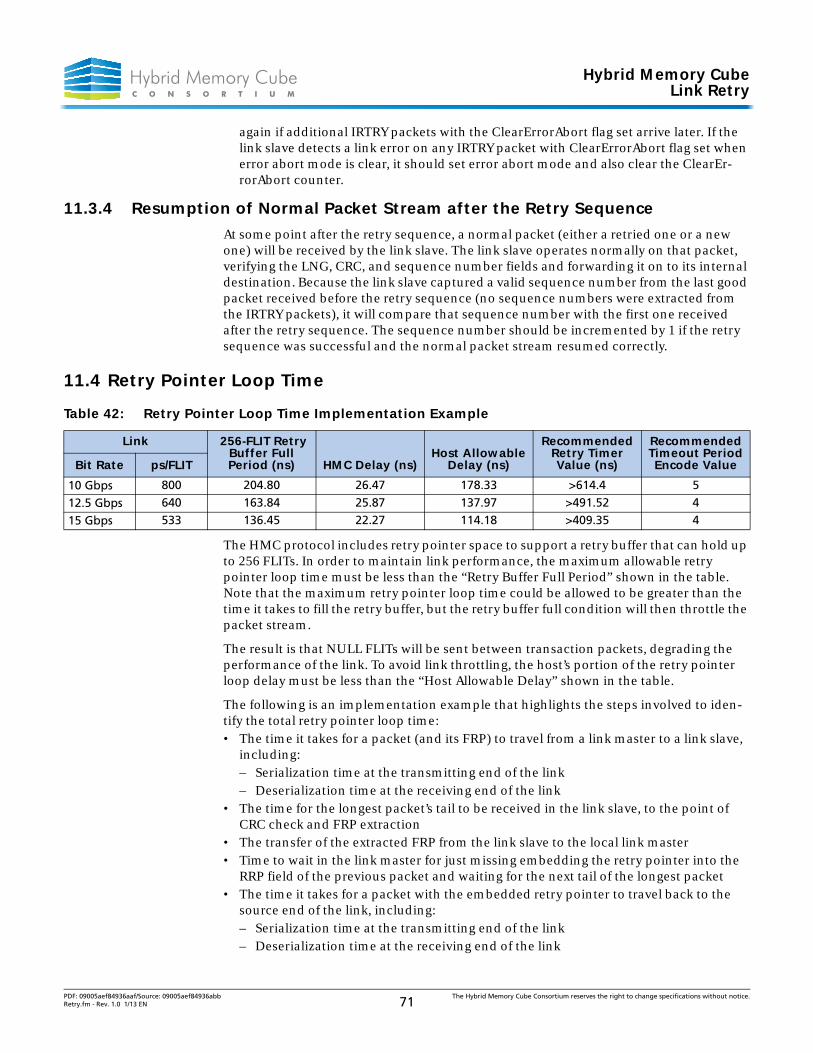
Hybrid Memory CubeLink Retry
again if additional IRTRY packets with the ClearErrorAbort flag set arrive later. If the link slave detects a link error on any IRTRY packet with ClearErrorAbort flag set when error abort mode is clear, it should set error abort mode and also clear the ClearEr-rorAbort counter.
11.3.4 Resumption of Normal Packet Stream after the Retry Sequence
At some point after the retry sequence, a normal packet (either a retried one or a new one) will be received by the link slave. The link slave operates normally on that packet, verifying the LNG, CRC, and sequence number fields and forwarding it on to its internal destination. Because the link slave captured a valid sequence number from the last good packet received before the retry sequence (no sequence numbers were extracted from the IRTRY packets), it will compare that sequence number with the first one received after the retry sequence. The sequence number should be incremented by 1 if the retry sequence was successful and the normal packet stream resumed correctly.
11.4 Retry Pointer Loop Time
The HMC protocol includes retry pointer space to support a retry buffer that can hold up to 256 FLITs. In order to maintain link performance, the maximum allowable retry pointer loop time must be less than the “Retry Buffer Full Period” shown in the table. Note that the maximum retry pointer loop time could be allowed to be greater than the time it takes to fill the retry buffer, but the retry buffer full condition will then throttle the packet stream.
The result is that NULL FLITs will be sent between transaction packets, degrading the performance of the link. To avoid link throttling, the host’s portion of the retry pointer loop delay must be less than the “Host Allowable Delay” shown in the table.
The following is an implementation example that highlights the steps involved to iden-tify the total retry pointer loop time:• The time it takes for a packet (and its FRP) to travel from a link master to a link slave,
including:– Serialization time at the transmitting end of the link– Deserialization time at the receiving end of the link
• The time for the longest packet’s tail to be received in the link slave, to the point of CRC check and FRP extraction
• The transfer of the extracted FRP from the link slave to the local link master• Time to wait in the link master for just missing embedding the retry pointer into the
RRP field of the previous packet and waiting for the next tail of the longest packet• The time it takes for a packet with the embedded retry pointer to travel back to the
source end of the link, including:– Serialization time at the transmitting end of the link– Deserialization time at the receiving end of the link
Table 42: Retry Pointer Loop Time Implementation Example
Link 256-FLIT Retry Buffer Full Period (ns) HMC Delay (ns)
Host Allowable Delay (ns)
Recommended Retry Timer Value (ns)
Recommended Timeout Period Encode ValueBit Rate ps/FLIT
10 Gbps 800 204.80 26.47 178.33 >614.4 5
12.5 Gbps 640 163.84 25.87 137.97 >491.52 4
15 Gbps 533 136.45 22.27 114.18 >409.35 4
PDF: 09005aef84936aaf/Source: 09005aef84936abb The Hybrid Memory Cube Consortium reserves the right to change specifications without notice.Retry.fm - Rev. 1.0 1/13 EN 71
Hybrid Memory CubeLink Retry
• Time for the longest packet’s tail to be received in the link slave, to the point of CRC check and RRP extraction
• The transfer of the RRP from the link slave to the local link master (the original trans-mitter in the first step)
11.5 Link Flow Control During Retry
When the normal packet stream is transmitted by the link master, it has already deter-mined that the link slave has enough buffer space in its buffers to accept all FLITs of the transmitted packets, as controlled by the return token count protocol. If a link error occurs and the packet stream is aborted during Error Abort mode in the link slave, the reserved space in the receive buffers still exists, and therefore, when those packets are retransmitted across the link, there is no need for any additional flow control, except for the following clarification. At the receiver, the link slave may poison the packet that has errored, but it has already propagated it forward into the receive buffer. Because this takes up some FLIT locations, the return token count control logic must not return the tokens for a poisoned packet. That packet will be retransmitted, and when it is finally loaded into the receive buffer with good CRC and propagated further, the tokens will be returned. All subsequent packets (after the errored one) dropped in the link slave will not be forwarded into the receive buffer, as a result, the buffer space will be available for those packets as they are retransmitted.
A consequence of forwarding the poisoned packet and not returning tokens until the packet is retransmitted successfully is as follows: The poisoned packet could have been the last packet that caused the full condition at the receive buffer, and then the receive buffer could be temporarily stalled due to downstream flow control. If this were the case, the failed packet would be the only packet to be transmitted. When the packet was retransmitted, there would be no room for that packet in the receive buffer. An easy solu-tion to this is to adjust the maximum tokens available for that receive buffer to 9 FLITs less than the actual buffer size. This accommodates an extra copy (the poisoned one) of the largest packet that could be retransmitted during a link retry.
11.6 Example Implementation Link Error and Retry Sequence
For the following example, refer to Figure 17 on page 62.
The green link master, upper left, transmits packets across the link to the green link slave in the upper right. The blue link master, lower right, transmits packets across the link to the blue link slave in the lower left.1. Successful green packets flowing from the green link master to the green link slave
across the top of the diagram. Green packets have green FRPs and blue RRPs embed-ded in them. Successful blue packets flowing from the blue link master to the blue linkslave across the bottom of the diagram. Blue packets have blue FRPs and green RRPsembedded in them.
2. An error occurs in the green packet stream across the top. The green link slave detects CRC error and sets error abort mode. The errored packet is poisoned and all following packets are dropped.
3. Flow of FRPs and RRPs stops from the green link slave to the blue link master.4. The blue link master receives the error abort mode signal from the green link slave,
suspends its normal packet stream from its output FIFO, and inserts a stream of IRTRY packets each with the StartRetry flag set (FRP[0] = 1). The blue link master embeds the latest FRP it received from the green link slave (via its retry pointer collec-tion register) into the RRP field of each IRTRY packet. The value embedded into the
PDF: 09005aef84936aaf/Source: 09005aef84936abb The Hybrid Memory Cube Consortium reserves the right to change specifications without notice.Retry.fm - Rev. 1.0 1/13 EN 72
Hybrid Memory CubeLink Retry
RRP field is the same as the FRP for the last good packet that was received at the green link slave before the link error occurred. After sending the stream of IRTRY packets, the blue link master resumes it normal packet stream from its output FIFO.
5. The blue link slave detects the IRTRY stream and counts the StartRetry flags. During this time it extracts the RRP and sends it to the green link master, which updates its retry buffer read pointer to point to the packet that had errored. When the IRTRY receive threshold is reached, the blue link slave sends a StartRetry pulse to the green link master.
6. The blue link slave continues to receive normal packets, forwarding them to its input FIFO, and extracts all RRPs, FRPs, and RTCs.
7. The green link master receives the StartRetry pulse which starts its retry sequence and enters into its LinkRetry_Begin state, finishes sending the current packet being trans-mitted from its output FIFO, then stops. That packet is the last packet that gets loaded into the retry buffer.
8. The green link master enters its LinkRetry_Init state and transmits a stream of IRTRY packets, each with the ClearErrorAbort flag set (FRP[1]=1). During this time, the green link master is receiving valid FRPs from the blue link slave (via its retry pointer collec-tion register), and it embeds those into the RRP field of every IRTRY packet.
9. The green link slave, currently in Error Abort mode, detects the stream of IRTRY pack-ets and counts the ClearErrorAbort flags. When it reaches the IRTRY receive threshold, it clears Error Abort mode. At that time it will begin extracting the RRPs from the IRTRY packet(s) and sends them to the blue link master.
10. The green link master enters its LinkRetry_FLIT state and transmits the pending packets from its retry buffer until its read pointer equals its write pointer. It continues to embed the latest value of its retry pointer collection register into the RRP field of each of the pending packets being retransmitted. As the pending packet stream com-pletes from the retry buffer, the green link master switches to new packets waiting in its output FIFO.
11. The green link slave receives the retried packet stream and resumes the sequence check (along with CRC check, etc). The first retried packet received should have a sequence number +1 greater than the last successfully received packet before the link error occurred. All successfully received retried packets, followed by new packets, will be forwarded to the link input FIFO.
PDF: 09005aef84936aaf/Source: 09005aef84936abb The Hybrid Memory Cube Consortium reserves the right to change specifications without notice.Retry.fm - Rev. 1.0 1/13 EN 73
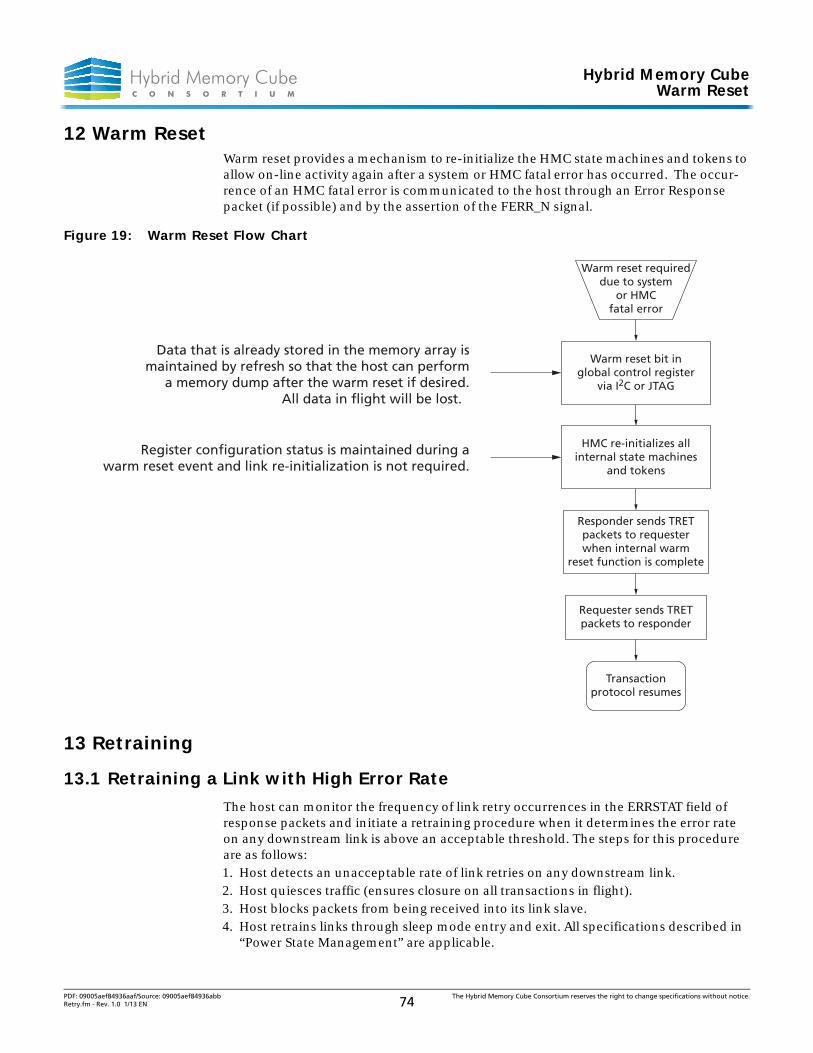
Hybrid Memory CubeWarm Reset
12 Warm ResetWarm reset provides a mechanism to re-initialize the HMC state machines and tokens to allow on-line activity again after a system or HMC fatal error has occurred. The occur-rence of an HMC fatal error is communicated to the host through an Error Response packet (if possible) and by the assertion of the FERR_N signal.
Figure 19: Warm Reset Flow Chart
13 Retraining
13.1 Retraining a Link with High Error Rate
The host can monitor the frequency of link retry occurrences in the ERRSTAT field of response packets and initiate a retraining procedure when it determines the error rate on any downstream link is above an acceptable threshold. The steps for this procedure are as follows:1. Host detects an unacceptable rate of link retries on any downstream link.2. Host quiesces traffic (ensures closure on all transactions in flight).3. Host blocks packets from being received into its link slave.4. Host retrains links through sleep mode entry and exit. All specifications described in
“Power State Management” are applicable.
Warm reset requireddue to system
or HMCfatal error
Warm reset bit inglobal control register
via I2C or JTAG
HMC re-initializes allinternal state machines
and tokens
Data that is already stored in the memory array ismaintained by refresh so that the host can perform
a memory dump after the warm reset if desired.All data in flight will be lost.
Register configuration status is maintained during awarm reset event and link re-initialization is not required.
Responder sends TRETpackets to requesterwhen internal warm
reset function is complete
Requester sends TRETpackets to responder
Transactionprotocol resumes
PDF: 09005aef84936aaf/Source: 09005aef84936abb The Hybrid Memory Cube Consortium reserves the right to change specifications without notice.Retry.fm - Rev. 1.0 1/13 EN 74
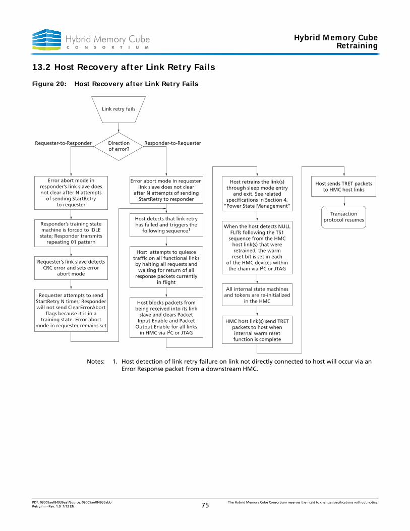
Hybrid Memory CubeRetraining
13.2 Host Recovery after Link Retry Fails
Figure 20: Host Recovery after Link Retry Fails
Notes: 1. Host detection of link retry failure on link not directly connected to host will occur via an Error Response packet from a downstream HMC.
Directionof error?
Requester-to-Responder Responder-to-Requester
Link retry fails
Error abort mode in requester link slave does not clear
after N attempts of sendingStartRetry to responder
Error abort mode inresponder’s link slave doesnot clear after N attempts
of sending StartRetryto requester
Responder’s training statemachine is forced to IDLEstate; Responder transmits
repeating 01 pattern
Requester’s link slave detectsCRC error and sets error
abort mode
Requester attempts to sendStartRetry N times; Responderwill not send ClearErrorAbort
flags because it is in atraining state. Error abort
mode in requester remains set
Host detects that link retryhas failed and triggers the
following sequence1
Host blocks packets frombeing received into its link
slave and clears PacketInput Enable and Packet
Output Enable for all linksin HMC via I2C or JTAG
Host retrains the link(s)through sleep mode entry
and exit. See relatedspecifications in Section 4,
“Power State Management”
When the host detects NULLFLITs following the TS1
sequence from the HMChost link(s) that wereretrained, the warm
reset bit is set in eachof the HMC devices withinthe chain via I2C or JTAG
All internal state machinesand tokens are re-initialized
in the HMC
Host attempts to quiescetraffic on all functional linksby halting all requests and
waiting for return of allresponse packets currently
in flight
HMC host link(s) send TRETpackets to host wheninternal warm resetfunction is complete
Host sends TRET packetsto HMC host links
Transactionprotocol resumes
PDF: 09005aef84936aaf/Source: 09005aef84936abb The Hybrid Memory Cube Consortium reserves the right to change specifications without notice.Retry.fm - Rev. 1.0 1/13 EN 75
Hybrid Memory CubeFunctional Characteristics
14 Functional Characteristics
14.1 Packet Ordering and Data Consistency
There can be multiple packet-reordering points within the HMC, including the following implementation examples:1. The output of each link slave input buffer could reorder packets arriving from one link
that are destined for different vaults. This would prevent a busy vault from blockingthe packet flow out of the receive buffer and enable the flow of packets across the linkto continue.
2. Each vault controller command queue could reorder packet execution to banks that are not busy, potentially optimizing the memory bus usage.
All reordering points within an HMC must maintain the order of a stream of packets from a specific link to a specific bank within a vault. This ensures that if a host sends a write request packet to address x followed by a read request packet to the same address x, the READ will always return the newly written data.
Packet ordering performed by the HMC supports messaging or data-passing program-ming between two or more hosts with access to the same HMC. This common method of host-to-host messaging is known as producer-consumer programming, and proceeds as follows: 1. Host 0 wants to pass a message/data to host 1. Host 0 writes memory location A (this
could be multiple locations) with the message/data.2. Upon receiving all expected successful write responses for the write(s) to location A,
host 0 sets a flag in memory location B indicating that the message/data is available in location A.
3. Host 1 executes a loop, polling (that is, issuing read requests to) location B to observe the set flag.
4. Upon detecting the set flag in the read response for location B, host 1 issues a read request to location A.
5. Host 1 receives the read response for location A containing the newly-written data from host 0.
This scenario proceeds as defined if host 0 waits for the successful write response for the write to location A before issuing the write request packet to location B.
The write response is generated at the vault controller after the write request is fully executed and is identified with the same tag as the write request. This write response could be an explicit write response packet, or it could optionally be embedded within a response packet being sent back on the same link. Locations A and B can be any memory locations. Note that this scenario is not supported with the use of posted write requests.
14.2 Data Access Performance Considerations
Due to the internal 32-byte granularity of the DRAM data bus within each vault in the HMC, inefficient utilization of this bus occurs when starting or ending on a 16-byte boundary rather than a 32-byte boundary. An extreme example of this would be the host issuing a series of 16-byte read requests. Each read request would fetch 32 bytes from the DRAM and return half of the data in the response packet, throwing away the other 16 bytes of data. For bandwidth optimization it is advantageous to issue requests with 32-byte granularity.
PDF: 09005aef84936aaf/Source: 09005aef84936abb The Hybrid Memory Cube Consortium reserves the right to change specifications without notice.Functional_Characteristics.fm - Rev. 1.0 1/13 EN 76
Hybrid Memory CubeFunctional Characteristics
If the host issues a series of commands that access portions of the same data block (as defined by the maximum block size) rather than issuing one request accessing the entire data block, two performance disadvantages exist:
1. The probability of bank conflicts will increase in the accessed vault. 2. The multiple request and response packets have additional header/tail overhead
on the link.
Because of this, it is desirable to perform commands with larger data sizes. In an example implementation, if a host has defined the maximum block size as 128 bytes and instead of issuing a 128-byte request to a specific location, it issues four consecutive 32-byte requests to the same block location. The cube will send these four independent requests to the specific bank whereby it must open and close the row in the same bank four times, reducing bandwidth utilization and increasing latency as compared to the case in which a single 128-byte request is issued.
To maximize bandwidth utilization and reduce system latency the following should be taken into consideration:
1. Request data block sizes that are as large as possible, up to the configured maxi-mum block size, that meet the requirements of the system.
2. Configure the maximum block size based upon the most frequently requested data size. If the most frequently requested data size does not equal any of the possible maximum block sizes (32B, 64B, or 128B), select the smallest block size that encompasses the most frequently requested data size. For example, if a system most often requires 48B data transfers, 64B should be chosen as the maximum block size.
14.3 Vault ECC and Reference Error Detection
Memory READ and WRITE operations have a parity bit added to the command and address signals that are sent from each vault controller to the memory partitions and banks associated with each controller. If the bank receiving a request determines that there is a parity error, the reference is retried.
Data is protected in memory using ECC. The ECC should provide correction of a single-bit error as well as all data bits that are transmitted over a single, failed TSV between the memory and the logic base.
Memory locations are initialized with correct ECC data patterns before the host begins using the locations. This eliminates a write-before-read requirement to avoid SBEs and MUEs.
14.4 Refresh
DRAM refresh is handled internally within the HMC by the vault controllers. As an example implementation, every vault controller could have a unique refresh rate for each of its bank groups (where a bank group is a set of banks within one memory die). An implementation may also choose to vary refresh rates dynamically, driven by condi-tions such as temperature and/or detected memory error rates.
14.5 Scrubbing
Scrubbing is used inside the cube to mitigate soft failures in memory. Two categories of scrubbing are provided in each vault controller:
PDF: 09005aef84936aaf/Source: 09005aef84936abb The Hybrid Memory Cube Consortium reserves the right to change specifications without notice.Functional_Characteristics.fm - Rev. 1.0 1/13 EN 77
Hybrid Memory CubeFunctional Characteristics
• Demand scrubbing: If a correctable error is detected in the read data of a read request, the data is corrected and returned to the host in the response packet. A scrubbing cycle is invoked that writes the corrected data back into the memory array.
• Patrol scrubbing: This form of scrubbing is performed by the cube refresh logic. If a correctable error is detected, a scrubbing cycle is invoked that writes the correct data back into the memory array.
The scrubbing cycle writes the corrected data immediately after the correctable error is discovered on the read. This read-update-write operation is atomic, meaning that no other reference to the location will be possible between the read and the associated write. This is handled as a bank conflict within the vault controller command queue.
All scrubbing cycles can be programmed to execute a reread of the scrubbed memory location to determine whether the scrubbing operation was successful. If it was successful, a “soft error” is logged. If it was unsuccessful and another correctable error occurs during the reread, a “hard error” is assumed and it is logged. Correctable errors that are designated as hard errors enable the system to continue to run, but they also increase the probability that the occurrence of another soft or hard error within the 16-byte ECC word will turn the correctable situation into an uncorrectable one. To cover this case, the HMC provides In-Field repair of the hard failures, the mechanism of which is vendor specific.
14.6 Response Open Loop Mode
During normal transaction layer packet flow, return token counts (RTCs) are returned in both directions on each link. This controls the flow of request packets in one direction and response packets in the other direction. Response open loop mode can be config-ured on the upstream links that are connected to the host. This mode eliminates the requirement for the host to send tokens back to the cube, and results in two simplifica-tions:• The host link slave does not have to generate tokens when response packets are
consumed. • The host link master does not have to embed any RTCs into request packets being
transmitted to the cube.
The response open loop mode will force the link master to send response packets to the host without the token requirements. (Other packet flow controls such as retry buffer full conditions and retry in progress will still suspend packet flow if necessary.)
PDF: 09005aef84936aaf/Source: 09005aef84936abb The Hybrid Memory Cube Consortium reserves the right to change specifications without notice.Functional_Characteristics.fm - Rev. 1.0 1/13 EN 78
Hybrid Memory CubeJTAG Interface
15 JTAG InterfaceHMC incorporates a standard test access port (TAP) controller that operates in accor-dance with IEEE Standard 1149.1-2001. The input and output signals of the test access port use VDD as a supply.
The JTAG test access port uses the TAP controller on the HMC, from which the instruc-tion, bypass, ID, boundary scan, and CADATA registers can be selected. Each of these functions of the TAP controller is described in detail below.
The HMC includes boundary scan support that complies with the IEEE 1149.1 and 1149.6 standards. Boundary scan chain order is provided within BSDL files for each HMC configuration.
15.1 Disabling the JTAG Feature
It is possible to operate HMC without using the JTAG feature. To disable the TAP controller, tie the Test Reset Signal, TRST_N, LOW. TCK, TDI, and TMS can all be consid-ered “Don’t Care” when TRST_N is LOW. TDO should be left unconnected. Upon power up, the device comes up in a reset state; this will not interfere with the operation of the HMC device.
15.2 Test Access Port (TAP)
15.2.1 Test Clock (TCK)
The test clock is used only with the TAP controller. All inputs are captured on the rising edge of TCK. All outputs are driven from the falling edge of TCK.
15.2.2 Test Mode Select (TMS)
The TMS input is used to issue commands to the TAP controller and is sampled on the rising edge of TCK.
All of the states in Figure 21: “TAP Controller State Diagram” on page 81 are entered through the serial input of the TMS pin. A 0 in the diagram represents a LOW on the TMS pin during the rising edge of TCK; a 1 represents a HIGH on TMS.
15.2.3 Test Reset (TRST_N)
The TRST_N input provides asynchronous initialization of the TAP controller. TRST_N must be LOW during power-up and track the transition timing of the system reset signal, P_RST_N. To ensure deterministic operation of the test logic, TMS should be held HIGH while the signal applied at TRST_N changes from LOW to HIGH.
15.2.4 Test Data-In (TDI)
The TDI pin is used to input test instructions and data into the registers serially and can be connected to the input of any registers. The register between TDI and TDO is selected by the instruction that is loaded into the TAP instruction register. For information on loading the instruction register, see Figure 25: “JTAG Operation – Loading Instruction Code and Shifting Out Data” on page 86. TDI is connected to the most significant bit (MSB) of any register (see Figure 22: “TAP Controller Block Diagram” on page 81).
PDF: 09005aef84936aaf/Source: 09005aef84936abb The Hybrid Memory Cube Consortium reserves the right to change specifications without notice.Sideband.fm - Rev. 1.0 1/13 EN 79
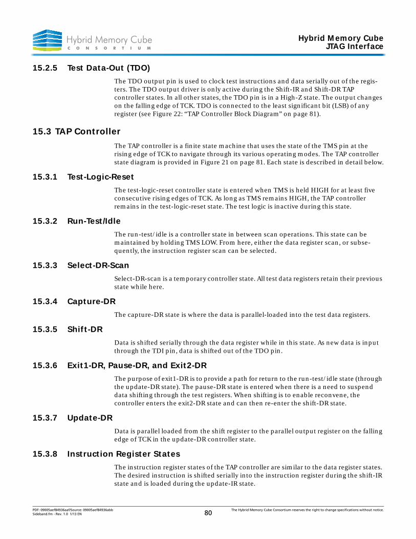
Hybrid Memory CubeJTAG Interface
15.2.5 Test Data-Out (TDO)
The TDO output pin is used to clock test instructions and data serially out of the regis-ters. The TDO output driver is only active during the Shift-IR and Shift-DR TAP controller states. In all other states, the TDO pin is in a High-Z state. The output changes on the falling edge of TCK. TDO is connected to the least significant bit (LSB) of any register (see Figure 22: “TAP Controller Block Diagram” on page 81).
15.3 TAP Controller
The TAP controller is a finite state machine that uses the state of the TMS pin at the rising edge of TCK to navigate through its various operating modes. The TAP controller state diagram is provided in Figure 21 on page 81. Each state is described in detail below.
15.3.1 Test-Logic-Reset
The test-logic-reset controller state is entered when TMS is held HIGH for at least five consecutive rising edges of TCK. As long as TMS remains HIGH, the TAP controller remains in the test-logic-reset state. The test logic is inactive during this state.
15.3.2 Run-Test/Idle
The run-test/idle is a controller state in between scan operations. This state can be maintained by holding TMS LOW. From here, either the data register scan, or subse-quently, the instruction register scan can be selected.
15.3.3 Select-DR-Scan
Select-DR-scan is a temporary controller state. All test data registers retain their previous state while here.
15.3.4 Capture-DR
The capture-DR state is where the data is parallel-loaded into the test data registers.
15.3.5 Shift-DR
Data is shifted serially through the data register while in this state. As new data is input through the TDI pin, data is shifted out of the TDO pin.
15.3.6 Exit1-DR, Pause-DR, and Exit2-DR
The purpose of exit1-DR is to provide a path for return to the run-test/idle state (through the update-DR state). The pause-DR state is entered when there is a need to suspend data shifting through the test registers. When shifting is to enable reconvene, the controller enters the exit2-DR state and can then re-enter the shift-DR state.
15.3.7 Update-DR
Data is parallel loaded from the shift register to the parallel output register on the falling edge of TCK in the update-DR controller state.
15.3.8 Instruction Register States
The instruction register states of the TAP controller are similar to the data register states. The desired instruction is shifted serially into the instruction register during the shift-IR state and is loaded during the update-IR state.
PDF: 09005aef84936aaf/Source: 09005aef84936abb The Hybrid Memory Cube Consortium reserves the right to change specifications without notice.Sideband.fm - Rev. 1.0 1/13 EN 80
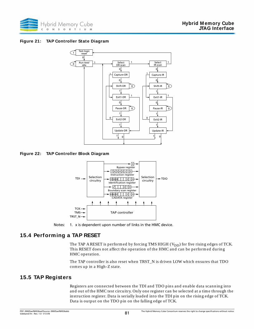
Hybrid Memory CubeJTAG Interface
Figure 21: TAP Controller State Diagram
Figure 22: TAP Controller Block Diagram
Notes: 1. x is dependent upon number of links in the HMC device.
15.4 Performing a TAP RESET
The TAP A RESET is performed by forcing TMS HIGH (VDD) for five rising edges of TCK. This RESET does not affect the operation of the HMC and can be performed during HMC operation.
The TAP controller is also reset when TRST_N is driven LOW which ensures that TDO comes up in a High-Z state.
15.5 TAP Registers
Registers are connected between the TDI and TDO pins and enable data scanning into and out of the HMC test circuitry. Only one register can be selected at a time through the instruction register. Data is serially loaded into the TDI pin on the rising edge of TCK. Data is output on the TDO pin on the falling edge of TCK.
Capture-IR
Shift-IR
Exit1-IR
Pause-IR
Exit2-IR
Update-IR
1
1
1
0
1 1
0 0
1 1
1
0
0
0
0 0
0
0
0 0
1
0
1
1
0
1
0
1
1
11 0
Test-logicreset
Run-test/idle
SelectIR-scan
SelectDR-scan
Capture-DR
Shift-DR
Exit1-DR
Pause-DR
Exit2-DR
Update-DR
0
01234567
012293031 ...
TCKTMS
TRST_N
Selectioncircuitry
Selectioncircuitry
TDOTDIIdentification register
012x1 ...
Boundary scan register
012616263 ...
CADATA register
Instruction register
TAP controller
Bypass register
PDF: 09005aef84936aaf/Source: 09005aef84936abb The Hybrid Memory Cube Consortium reserves the right to change specifications without notice.Sideband.fm - Rev. 1.0 1/13 EN 81

Hybrid Memory CubeJTAG Interface
15.5.1 Instruction Register
Eight-bit instructions can be loaded serially into the instruction register. This register is loaded during the update-IR state of the TAP controller. Upon power up, the instruction register is loaded with the IDCODE instruction. It is also loaded with the IDCODE instruction if the controller is placed in a reset state as described in the previous section.
When the TAP controller is in the capture-IR state, the two LSBs are loaded with a binary 01 pattern to accommodate fault isolation of the board-level serial test data path.
15.5.2 Bypass Register
To save time when shifting data serially through registers, it is sometimes advantageous to skip certain chips. The bypass register is a single-bit register that can be placed between the TDI and TDO pins. This enables data shifting through the HMC with minimal delay. The bypass register is set LOW (VSS) when the BYPASS instruction is executed.
15.5.3 Identification (ID) Register
The ID register is loaded with a vendor-specific, 32-bit code during the capture-DR state when the IDCODE command is loaded in the instruction register. The IDCODE is hard-wired into the HMC and can be shifted out when the TAP controller is in the shift-DR state. The ID register has a vendor code and other device-specific information described in Table 45 on page 87.
15.5.4 Boundary Scan Register
The boundary-scan register is loaded with the contents of the I/O ring when the TAP controller is in the capture-DR state and is then placed between the TDI and TDO balls when the controller is moved to the shift-DR state.
The behavior of the boundary scan register is completely specified by the IEEE 1149.1 standard.
15.5.5 CADATA Register
The CADATA is a 64-bit register used for configuration and status register access. This register is not defined by the IEEE 1149.1 standard.
15.6 TAP Instruction Set
15.6.1 Overview
Many different instructions are possible with the 8-bit instruction register. All combina-tions used are listed in Table 47 on page 88. These instructions are described in detail below. The remaining instructions are reserved and must not be used.
The TAP controller used in this HMC is fully compliant with the 1149.1 convention.
Table 43: CADATA Register
Register Name Sub-block Description
CADATA ADRS[63:32] Stores the address for configuration and status register access.DATA[31:0] 1) Stores data to be written during configuration write operations.
2) Stores results of configuration read operations.
PDF: 09005aef84936aaf/Source: 09005aef84936abb The Hybrid Memory Cube Consortium reserves the right to change specifications without notice.Sideband.fm - Rev. 1.0 1/13 EN 82
Hybrid Memory CubeJTAG Interface
Instructions are loaded into the TAP controller during the shift-IR state when the instruction register is placed between TDI and TDO. During this state, instructions are shifted through the instruction register through via the TDI and TDO pins. To execute the instruction after it is shifted into the controller, the TAP controller must be moved into the update-IR state.
15.6.2 EXTEST
The EXTEST instruction enables circuitry external to the component package to be tested. Boundary-scan register cells at output balls are used to apply a test vector, while those at input balls capture test results.
15.6.3 EXTEST_PULSE & EXTEST_TRAIN
The EXTEST_PULSE and EXTREST_TRAIN instructions provide an edge-detecting test mechanism for AC-coupled signals. The EXTEST_PULSE instruction provides a pulse of data onto an AC signal whereby the pulse width is controlled by the time spent in the Run-Test/Idle TAP Controller state. This produces a single “wide” pulse with a variable and controllable period. The EXTEST_TRAIN instruction provides a pulse train, the edges of which are generated by each falling edge of TCK while in the Run-Test/Idle TAP Controller state. DC pins behave according to the IEEE Std 1149.1 EXTEST instruction when either the EXTEST_PULSE or EXTEST_TRAIN instructions are selected.
15.6.4 HIGH-Z
The High-Z instruction causes the bypass register to be connected between the TDI and TDO. This places all HMC outputs into a High-Z state.
15.6.5 CLAMP
When the CLAMP instruction is loaded into the instruction register, the data driven by the output balls are determined from the values held in the boundary-scan register.
15.6.6 SAMPLE/PRELOAD
When the SAMPLE/PRELOAD instruction is loaded into the instruction register and the TAP controller is in the capture-DR state, a snapshot can be taken of the states of the component's input and output signals without interfering with the normal operation of the assembled board. The snapshot is taken on the rising edge of TCK and is captured in the boundary-scan register. The data can then be viewed by shifting through the compo-nents TDO output.
15.6.7 IDCODE
The IDCODE instruction causes loading of a vendor-specific, 32-bit code to be loaded into the instruction register. It also places the instruction register between the TDI and TDO pins and enables shifting the IDCODE out of the device when the TAP controller enters the shift-DR state. The IDCODE instruction is loaded into the instruction register upon power-up or whenever the TAP controller is given a test logic reset state.
15.6.8 BYPASS
When the BYPASS instruction is loaded in the instruction register and the TAP is placed in a shift-DR state, the bypass register is placed between TDI and TDO.
PDF: 09005aef84936aaf/Source: 09005aef84936abb The Hybrid Memory Cube Consortium reserves the right to change specifications without notice.Sideband.fm - Rev. 1.0 1/13 EN 83
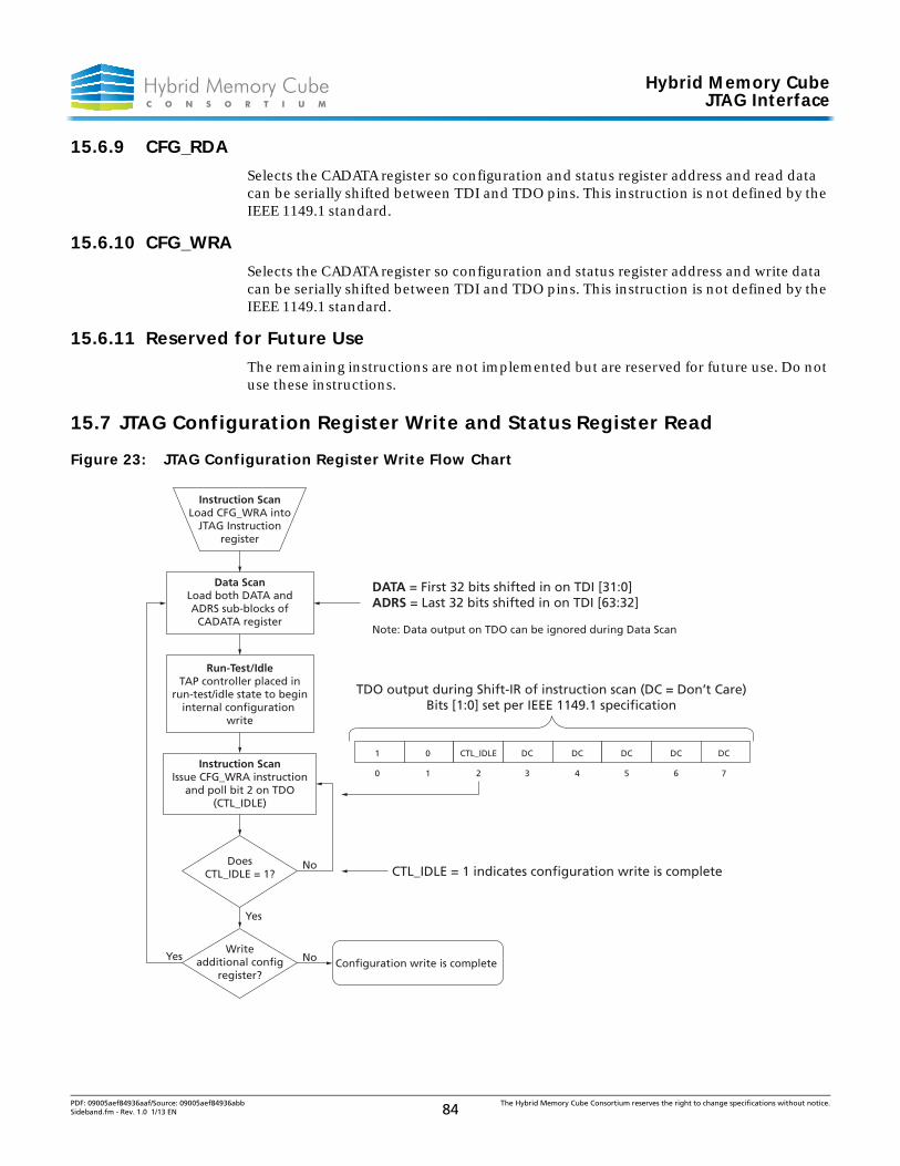
Hybrid Memory CubeJTAG Interface
15.6.9 CFG_RDA
Selects the CADATA register so configuration and status register address and read data can be serially shifted between TDI and TDO pins. This instruction is not defined by the IEEE 1149.1 standard.
15.6.10 CFG_WRA
Selects the CADATA register so configuration and status register address and write data can be serially shifted between TDI and TDO pins. This instruction is not defined by the IEEE 1149.1 standard.
15.6.11 Reserved for Future Use
The remaining instructions are not implemented but are reserved for future use. Do not use these instructions.
15.7 JTAG Configuration Register Write and Status Register Read
Figure 23: JTAG Configuration Register Write Flow Chart
Instruction ScanLoad CFG_WRA into
JTAG Instructionregister
Data ScanLoad both DATA andADRS sub-blocks of
CADATA register
Instruction ScanIssue CFG_WRA instruction
and poll bit 2 on TDO(CTL_IDLE)
Configuration write is complete
Run-Test/IdleTAP controller placed in
run-test/idle state to begininternal configuration
write
DoesCTL_IDLE = 1?
Yes
No
DATA = First 32 bits shifted in on TDI [31:0]ADRS = Last 32 bits shifted in on TDI [63:32]
Note: Data output on TDO can be ignored during Data Scan
TDO output during Shift-IR of instruction scan (DC = Don’t Care)Bits [1:0] set per IEEE 1149.1 specification
Writeadditional config
register?
NoYes
CTL_IDLE = 1 indicates configuration write is complete
1
0 1 2 3 4 5 6 7
0 CTL_IDLE DC DC DC DC DC
PDF: 09005aef84936aaf/Source: 09005aef84936abb The Hybrid Memory Cube Consortium reserves the right to change specifications without notice.Sideband.fm - Rev. 1.0 1/13 EN 84
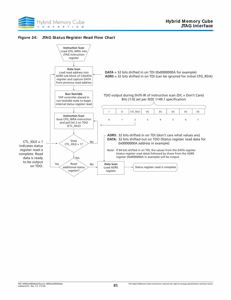
Hybrid Memory CubeJTAG Interface
Figure 24: JTAG Status Register Read Flow Chart
Instruction ScanLoad CFG_WRA into
JTAG Instructionregister
Data ScanLoad read address into
ADRS sub-block of CADATAregister and capture DATAfrom previous read address
Data ScanLoad ADRS
register
Instruction ScanIssue CFG_WRA instruction
and poll bit 2 on TDO(CTL_IDLE)
Run-Test/IdleTAP controller placed in
run-test/idle state to begininternal status register read
DoesCTL_IDLE = 1?
Yes
No
DATA = 32 bits shifted in on TDI (0x0000000A for example)ADRS = 32 bits shifted in on TDI (can be ignored for initial CFG_RDA)
TDO output during Shift-IR of instruction scan (DC = Don’t Care)Bits [1:0] set per IEEE 1149.1 specification
Readadditional status
register?
NoYes
ADRS: 32 bits shifted in on TDI (don’t care what values are)DATA: 32 bits shifted out on TDO (Status register read data for 0x0000000A address in example)
Note: If 64 bits shifted in on TDI, the values from the DATA register (status register read data) followed by those from the ADRS register (0x0000000A in example) will be output.
1
0 1 2 3 4 5 6 7
0 CTL_IDLE DC DC DC DC DC
Status register read is complete
CTL_IDLE = 1indicates statusregister read is
complete. Readdata is readyto be output
on TDO.
PDF: 09005aef84936aaf/Source: 09005aef84936abb The Hybrid Memory Cube Consortium reserves the right to change specifications without notice.Sideband.fm - Rev. 1.0 1/13 EN 85
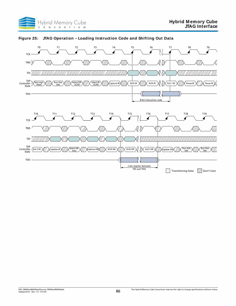
Hybrid Memory CubeJTAG Interface
Figure 25: JTAG Operation – Loading Instruction Code and Shifting Out Data
TMS
TDI
TCK
TDO
T0 T1 T2 T3 T4 T5 T6 T7 T8 T9
TAPController
State
Test-Logic-Reset
Run-TestIdle Capture-IRSelect-DR-
SCANSelect-IR-
SCAN Pause-IR Pause-IRShift-IR Exit 1-IR
8-bit instruction code
Don’t CareTransitioning Data
TMS
TDI
TCK
TDO
TAPController
State
T10 T11 T12 T13 T14 T15 T16 T17 T18
Exit 2-IR Select-DR-Scan
Capture-DR Shift-DR Shift-DR Exit1-DR Update-DR Run-TestIdleUpdate-IR
n-bit register betweenTDI and TDO
T19
Run-TestIdle
Shift-IR
PDF: 09005aef84936aaf/Source: 09005aef84936abb The Hybrid Memory Cube Consortium reserves the right to change specifications without notice.Sideband.fm - Rev. 1.0 1/13 EN 86
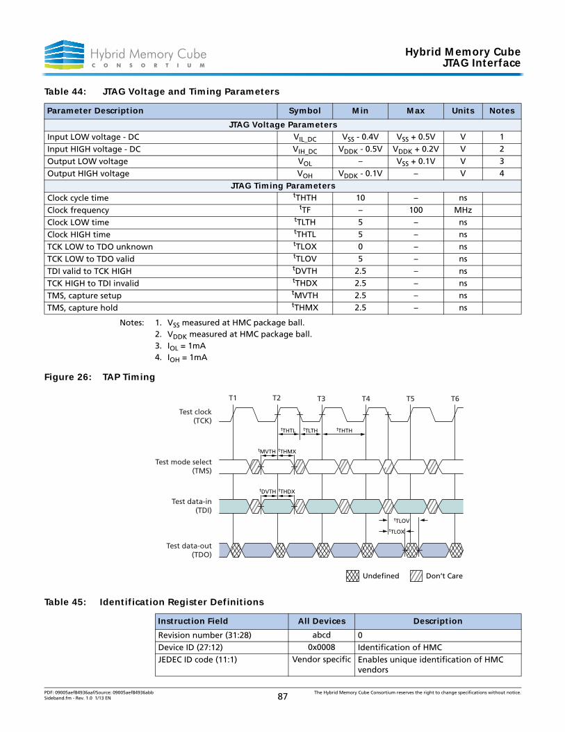
Hybrid Memory CubeJTAG Interface
Notes: 1. VSS measured at HMC package ball.2. VDDK measured at HMC package ball.3. IOL = 1mA4. IOH = 1mA
Figure 26: TAP Timing
Table 44: JTAG Voltage and Timing Parameters
Parameter Description Symbol Min Max Units Notes
JTAG Voltage ParametersInput LOW voltage - DC VIL_DC VSS - 0.4V VSS + 0.5V V 1
Input HIGH voltage - DC VIH_DC VDDK - 0.5V VDDK + 0.2V V 2
Output LOW voltage VOL – VSS + 0.1V V 3
Output HIGH voltage VOH VDDK - 0.1V – V 4
JTAG Timing ParametersClock cycle time tTHTH 10 – ns
Clock frequency tTF – 100 MHz
Clock LOW time tTLTH 5 – ns
Clock HIGH time tTHTL 5 – ns
TCK LOW to TDO unknown tTLOX 0 – ns
TCK LOW to TDO valid tTLOV 5 – ns
TDI valid to TCK HIGH tDVTH 2.5 – ns
TCK HIGH to TDI invalid tTHDX 2.5 – ns
TMS, capture setup tMVTH 2.5 – ns
TMS, capture hold tTHMX 2.5 – ns
Table 45: Identification Register Definitions
Instruction Field All Devices Description
Revision number (31:28) abcd 0Device ID (27:12) 0x0008 Identification of HMCJEDEC ID code (11:1) Vendor specific Enables unique identification of HMC
vendors
Don’t Care
tTLTHtTHTL tTHTH
tTHMXtMVTH
tTHDXtDVTH
tTLOX
tTLOV
Undefined
Test clock(TCK)
Test mode select(TMS)
Test data-in(TDI)
Test data-out(TDO)
T1 T2 T3 T4 T5 T6
PDF: 09005aef84936aaf/Source: 09005aef84936abb The Hybrid Memory Cube Consortium reserves the right to change specifications without notice.Sideband.fm - Rev. 1.0 1/13 EN 87
Hybrid Memory CubeJTAG Interface
ID register presence indicator (0) 1 Indicates the presence of an ID register
Table 46: Scan Register Sizes
Register Name Bit Size
Instruction 8
Bypass 1
Device ID 32
Boundary scan Dependent on number of links
CADATA 64
Table 47: Instruction Codes
Instruction Code Active Register Description
SAMPLE/PRELOAD 0x01 Boundary Scan 1149.1 SAMPLE/PRELOAD instructionIDCODE 0x02 Device ID 1149.1 IDCODE instructionCLAMP 0x04 Boundary Scan 1149.1 CLAMP instructionHIGHZ 0x08 Boundary Scan 1149.1 HIGHZ instructionEXTEST 0x09 Boundary Scan 1149.1 EXTEST instructionEXTEST_PULSE 0x0A Boundary Scan 1149.6 EXTEST_PULSE instructionEXTEST_TRAIN 0x0B Boundary Scan 1149.6 EXTEST_TRAIN instructionCFG_RDA 0x2C CADATA Allows Configuration & Status Register to be readCFG_WRA 0x2D CADATA Allows Configuration & Status Register to be writtenBYPASS 0xFF BYPASS 1149.1 BYPASS instruction
Table 45: Identification Register Definitions (Continued)
Instruction Field All Devices Description
PDF: 09005aef84936aaf/Source: 09005aef84936abb The Hybrid Memory Cube Consortium reserves the right to change specifications without notice.Sideband.fm - Rev. 1.0 1/13 EN 88
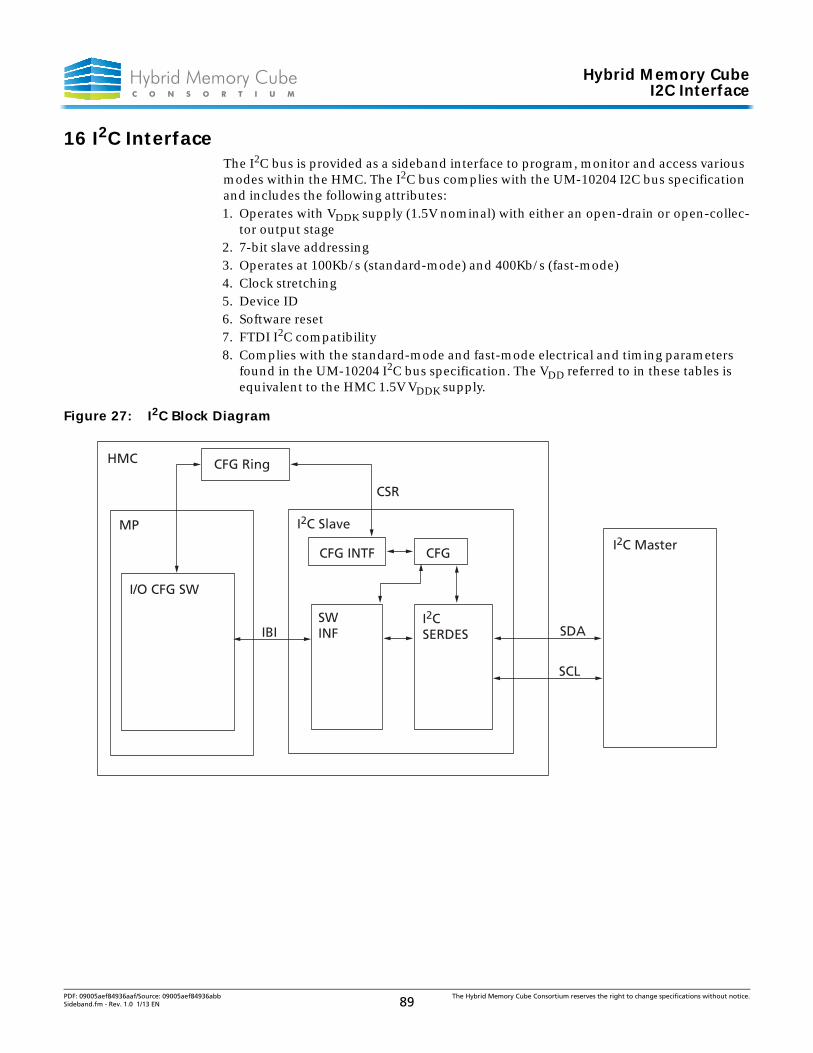
Hybrid Memory CubeI2C Interface
16 I2C InterfaceThe I2C bus is provided as a sideband interface to program, monitor and access various modes within the HMC. The I2C bus complies with the UM-10204 I2C bus specification and includes the following attributes:1. Operates with VDDK supply (1.5V nominal) with either an open-drain or open-collec-
tor output stage2. 7-bit slave addressing3. Operates at 100Kb/s (standard-mode) and 400Kb/s (fast-mode)4. Clock stretching5. Device ID6. Software reset7. FTDI I2C compatibility8. Complies with the standard-mode and fast-mode electrical and timing parameters
found in the UM-10204 I2C bus specification. The VDD referred to in these tables is equivalent to the HMC 1.5V VDDK supply.
Figure 27: I2C Block Diagram
CFG INTF CFG
SWINF
I2CSERDES
I2C Master
I2C Slave
CFG Ring
I/O CFG SW
HMC
MP
SDA
SCL
IBI
CSR
PDF: 09005aef84936aaf/Source: 09005aef84936abb The Hybrid Memory Cube Consortium reserves the right to change specifications without notice.Sideband.fm - Rev. 1.0 1/13 EN 89
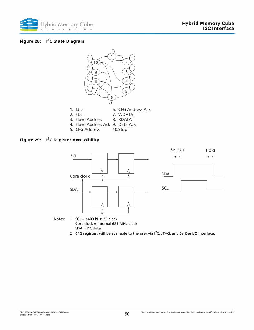
Hybrid Memory CubeI2C Interface
Figure 28: I2C State Diagram
Figure 29: I2C Register Accessibility
Notes: 1. SCL = 400 kHz I2C clockCore clock = Internal 625 MHz clockSDA = I2C data
2. CFG registers will be available to the user via I2C, JTAG, and SerDes I/O interface.
12
3
4
56
7
8
9
10
1. Idle2. Start3. Slave Address4. Slave Address Ack5. CFG Address
6. CFG Address Ack7. WDATA8. RDATA9. Data Ack10. Stop
SCL
Core clock
SDA SCL
SDA
Set-Up Hold
PDF: 09005aef84936aaf/Source: 09005aef84936abb The Hybrid Memory Cube Consortium reserves the right to change specifications without notice.Sideband.fm - Rev. 1.0 1/13 EN 90
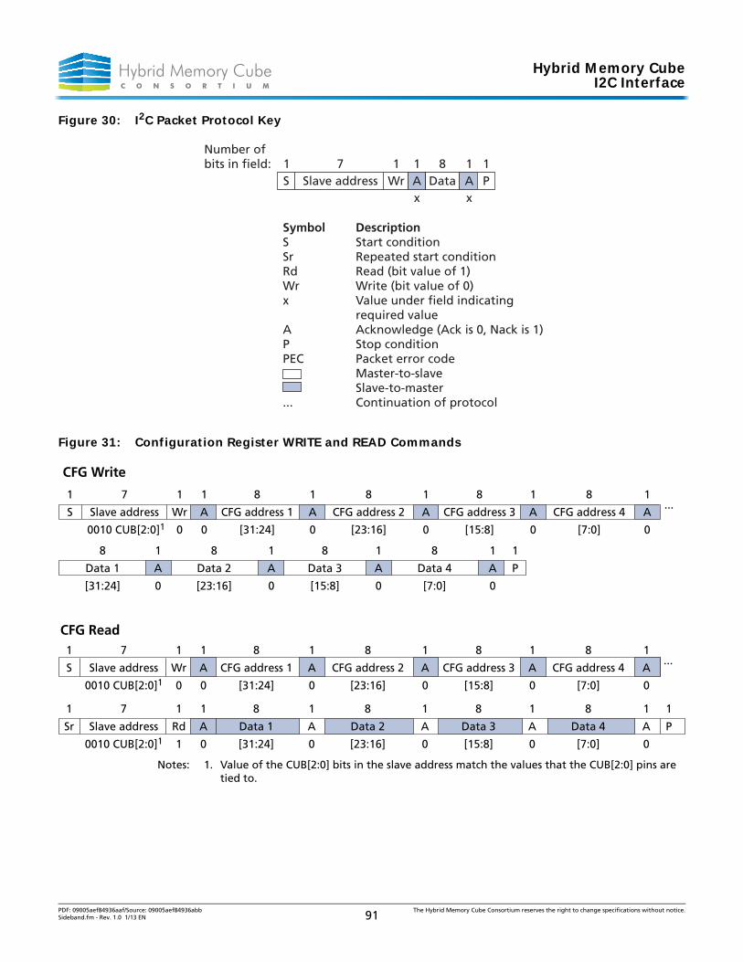
Hybrid Memory CubeI2C Interface
Figure 30: I2C Packet Protocol Key
Figure 31: Configuration Register WRITE and READ Commands
Notes: 1. Value of the CUB[2:0] bits in the slave address match the values that the CUB[2:0] pins are tied to.
Symbol DescriptionS Start conditionSr Repeated start conditionRd Read (bit value of 1)Wr Write (bit value of 0)x Value under field indicating required valueA Acknowledge (Ack is 0, Nack is 1)P Stop conditionPEC Packet error code Master-to-slave Slave-to-master... Continuation of protocol
Number of bits in field: 1 7 1 1 8 1 1 S Slave address Wr A Data A P x x
CFG Write
CFG Read
1
S
1
Wr
0
1
A
0
1
A
0
7
Slave address
0010 CUB[2:0]1
8
CFG address 1
[31:24]
8
CFG address 2
[23:16]
1
A
0
8
CFG address 3
[15:8]
1
A
0
1
A
0
...8
CFG address 4
[7:0]
1
A
0
8
Data 1
[31:24]
8
Data 2
[23:16]
1
A
0
8
Data 3
[15:8]
1
A
0
1
A
0
1
P
8
Data 4
[7:0]
1
S
1
Wr
0
1
A
0
1
A
0
7
Slave address
0010 CUB[2:0]1
1
Sr
1
Rd
1
1
A
0
7
Slave address
0010 CUB[2:0]1
8
CFG address 1
[31:24]
8
CFG address 2
[23:16]
1
A
0
8
CFG address 3
[15:8]
1
A
0
1
A
0
...8
CFG address 4
[7:0]
1
A
0
8
Data 1
[31:24]
8
Data 2
[23:16]
1
A
0
8
Data 3
[15:8]
1
A
0
1
A
0
1
P
8
Data 4
[7:0]
PDF: 09005aef84936aaf/Source: 09005aef84936abb The Hybrid Memory Cube Consortium reserves the right to change specifications without notice.Sideband.fm - Rev. 1.0 1/13 EN 91
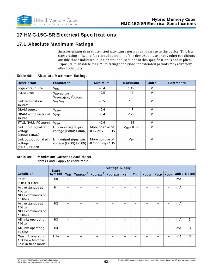
Hybrid Memory CubeHMC-15G-SR Electrical Specifications
17 HMC-15G-SR Electrical Specifications
17.1 Absolute Maximum Ratings
Stresses greater than those listed may cause permanent damage to the device. This is a stress rating only, and functional operation of the device at these or any other conditions outside those indicated in the operational sections of this specification is not implied. Exposure to absolute maximum rating conditions for extended periods may adversely affect reliability.
Table 48: Absolute Maximum Ratings
Description Parameter Minimum Maximum Units Comments
Logic core source VDD –0.4 1.15 V
PLL sources VDDPLLA[3:0], VDDPLLB[3:0], VDDPLLR
–0.5 1.4 V
Link termination sources
VTT, VTR –0.5 1.5 V
DRAM source VDDM –0.4 1.7 V
DRAM wordline boost source
VCCP –0.4 2.75 V
JTAG, NVM, I2C source VDDK –0.4 1.95 V
Link input signal pin voltage(LxRXP, LxRXN)
Link input signal pin voltage (LxRXP, LxRXN)
More positive of –0.1V or VTR - 1.1V
VTR + 0.3V V
Link output signal pin voltage(LxTXP, LxTXN)
Link output signal pin voltage (LxTXP, LxTXN)
More positive of–0.1V or VTT - 1.1V
VTT V
Table 49: Maximum Current ConditionsNotes 1 and 2 apply to entire table
ConditionState
Symbol
Voltage Supply
Units NotesVDD VDDPLLA4 VDDPLLB
4 VDDPLLR VTT VTR VDDM VCCP VDDK
Reset P_RST_N LOW
H0 – – – – – – – – – mA
Active standby at 10Gb/sNULL commands on all links
H1 – – – – – – – – – mA
Active standby at 15Gb/sNULL commands on all links
H2 – – – – – – – – – mA
All links operating 15Gb/s
H3 – – – – – – – – – mA 3
All links operating 10 Gb/s
H4 – – – – – – – – – mA 3
One link operating 15 Gb/s – All other links in sleep mode
H5a – – – – – – – – – mA 3
PDF: 09005aef84936aaf/Source: 09005aef84936abb The Hybrid Memory Cube Consortium reserves the right to change specifications without notice.15G-SR_Electrical_Specifications.fm - Rev. 1.0 1/13 EN 92
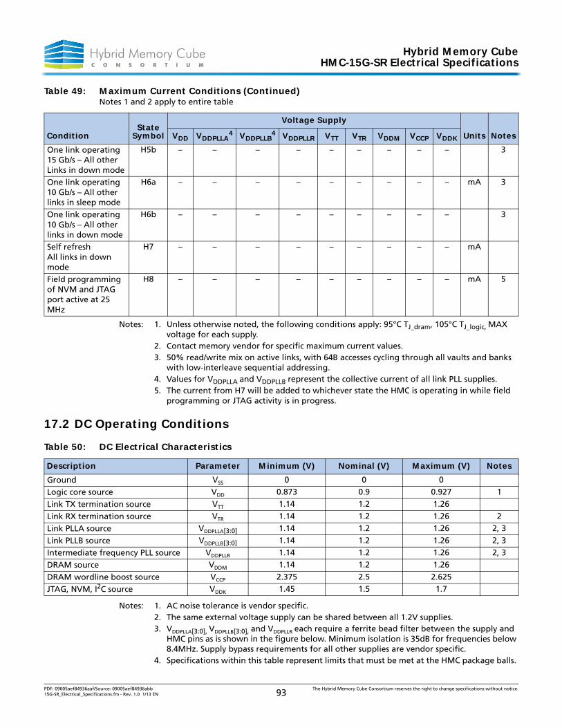
Hybrid Memory CubeHMC-15G-SR Electrical Specifications
Notes: 1. Unless otherwise noted, the following conditions apply: 95°C TJ_dram, 105°C TJ_logic, MAX voltage for each supply.
2. Contact memory vendor for specific maximum current values.3. 50% read/write mix on active links, with 64B accesses cycling through all vaults and banks
with low-interleave sequential addressing.4. Values for VDDPLLA and VDDPLLB represent the collective current of all link PLL supplies.5. The current from H7 will be added to whichever state the HMC is operating in while field
programming or JTAG activity is in progress.
17.2 DC Operating Conditions
Notes: 1. AC noise tolerance is vendor specific.2. The same external voltage supply can be shared between all 1.2V supplies.3. VDDPLLA[3:0], VDDPLLB[3:0], and VDDPLLR each require a ferrite bead filter between the supply and
HMC pins as is shown in the figure below. Minimum isolation is 35dB for frequencies below 8.4MHz. Supply bypass requirements for all other supplies are vendor specific.
4. Specifications within this table represent limits that must be met at the HMC package balls.
One link operating 15 Gb/s – All other Links in down mode
H5b – – – – – – – – – 3
One link operating 10 Gb/s – All other links in sleep mode
H6a – – – – – – – – – mA 3
One link operating 10 Gb/s – All other links in down mode
H6b – – – – – – – – – 3
Self refreshAll links in down mode
H7 – – – – – – – – – mA
Field programming of NVM and JTAG port active at 25 MHz
H8 – – – – – – – – – mA 5
Table 50: DC Electrical Characteristics
Description Parameter Minimum (V) Nominal (V) Maximum (V) Notes
Ground VSS 0 0 0
Logic core source VDD 0.873 0.9 0.927 1
Link TX termination source VTT 1.14 1.2 1.26
Link RX termination source VTR 1.14 1.2 1.26 2
Link PLLA source VDDPLLA[3:0] 1.14 1.2 1.26 2, 3
Link PLLB source VDDPLLB[3:0] 1.14 1.2 1.26 2, 3
Intermediate frequency PLL source VDDPLLR 1.14 1.2 1.26 2, 3
DRAM source VDDM 1.14 1.2 1.26
DRAM wordline boost source VCCP 2.375 2.5 2.625
JTAG, NVM, I2C source VDDK 1.45 1.5 1.7
Table 49: Maximum Current Conditions (Continued)Notes 1 and 2 apply to entire table
ConditionState
Symbol
Voltage Supply
Units NotesVDD VDDPLLA4 VDDPLLB
4 VDDPLLR VTT VTR VDDM VCCP VDDK
PDF: 09005aef84936aaf/Source: 09005aef84936abb The Hybrid Memory Cube Consortium reserves the right to change specifications without notice.15G-SR_Electrical_Specifications.fm - Rev. 1.0 1/13 EN 93
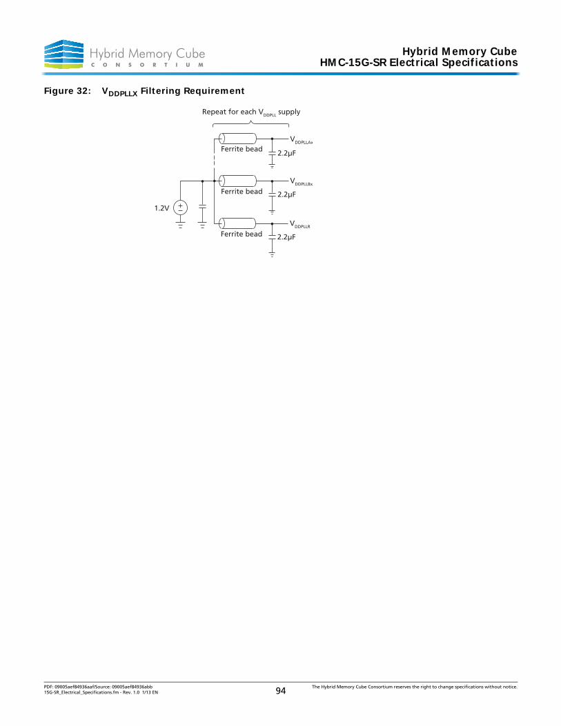
Hybrid Memory CubeHMC-15G-SR Electrical Specifications
Figure 32: VDDPLLX Filtering Requirement
VDDPLLBx
VDDPLLAx
Repeat for each VDDPLL supply
Ferrite bead 2.2μF
1.2V
2.2μF
VDDPLLR
Ferrite bead 2.2μF
Ferrite bead
PDF: 09005aef84936aaf/Source: 09005aef84936abb The Hybrid Memory Cube Consortium reserves the right to change specifications without notice.15G-SR_Electrical_Specifications.fm - Rev. 1.0 1/13 EN 94
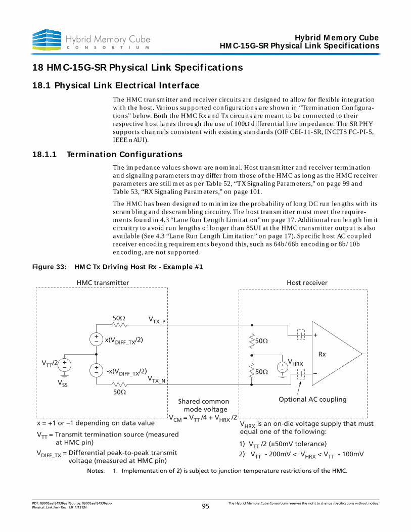
Hybrid Memory CubeHMC-15G-SR Physical Link Specifications
18 HMC-15G-SR Physical Link Specifications
18.1 Physical Link Electrical Interface
The HMC transmitter and receiver circuits are designed to allow for flexible integration with the host. Various supported configurations are shown in “Termination Configura-tions” below. Both the HMC Rx and Tx circuits are meant to be connected to their respective host lanes through the use of 100differential line impedance. The SR PHY supports channels consistent with existing standards (OIF CEI-11-SR, INCITS FC-PI-5, IEEE nAUI).
18.1.1 Termination Configurations
The impedance values shown are nominal. Host transmitter and receiver termination and signaling parameters may differ from those of the HMC as long as the HMC receiver parameters are still met as per Table 52, “TX Signaling Parameters,” on page 99 and Table 53, “RX Signaling Parameters,” on page 101.
The HMC has been designed to minimize the probability of long DC run lengths with its scrambling and descrambling circuitry. The host transmitter must meet the require-ments found in 4.3 “Lane Run Length Limitation” on page 17. Additional run length limit circuitry to avoid run lengths of longer than 85UI at the HMC transmitter output is also available (See 4.3 “Lane Run Length Limitation” on page 17). Specific host AC coupled receiver encoding requirements beyond this, such as 64b/66b encoding or 8b/10b encoding, are not supported.
Figure 33: HMC Tx Driving Host Rx - Example #1
Notes: 1. Implementation of 2) is subject to junction temperature restrictions of the HMC.
50
50
HMC transmitter Host receiver
+
–
50
50
-x(VDIFF_TX/2)
x(VDIFF_TX/2)
VTX_P
VTX_N
VTT/2
VSS
Rx
+–
VHRX
VHRX is an on-die voltage supply that must equal one of the following:
+_
+–
+–
x = +1 or –1 depending on data value
VTT = Transmit termination source (measured at HMC pin)
Shared common mode voltage
VCM = VTT /4 + VHRX /2
VDIFF_TX = Differential peak-to-peak transmit voltage (measured at HMC pin)
Optional AC coupling
2) VTT - 200mV < VHRX < VTT - 100mV
1) VTT /2 (±50mV tolerance)
PDF: 09005aef84936aaf/Source: 09005aef84936abb The Hybrid Memory Cube Consortium reserves the right to change specifications without notice.Physical_Link.fm - Rev. 1.0 1/13 EN 95
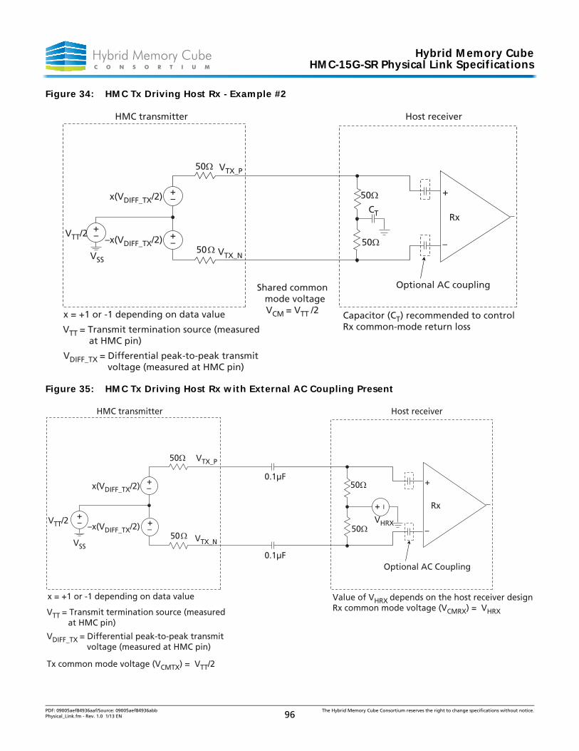
Hybrid Memory CubeHMC-15G-SR Physical Link Specifications
Figure 34: HMC Tx Driving Host Rx - Example #2
Figure 35: HMC Tx Driving Host Rx with External AC Coupling Present
50
50
CT
HMC transmitter Host receiver
+
–
50
50–x(VDIFF_TX/2)
x(VDIFF_TX/2)
VTX_P
VTX_N
VTT/2
VSS
Rx
+–
+–
+–
x = +1 or -1 depending on data value
VTT = Transmit termination source (measured at HMC pin)
Shared common mode voltageVCM = VTT /2 Capacitor (CT) recommended to control
Rx common-mode return loss
Optional AC coupling
VDIFF_TX = Differential peak-to-peak transmit voltage (measured at HMC pin)
50
500.1μF
0.1μF
HMC transmitter Host receiver
+
–
50
50–x(VDIFF_TX/2)
x(VDIFF_TX/2)
VTX_P
VTX_N
VTT/2
VSS
Rx
+–
+–
+–
x = +1 or -1 depending on data value
VTT = Transmit termination source (measured at HMC pin) VDIFF_TX = Differential peak-to-peak transmit voltage (measured at HMC pin)
VHRX
Value of VHRX depends on the host receiver designRx common mode voltage (VCMRX) = VHRX
+ –
Optional AC Coupling
Tx common mode voltage (VCMTX) = VTT/2
PDF: 09005aef84936aaf/Source: 09005aef84936abb The Hybrid Memory Cube Consortium reserves the right to change specifications without notice.Physical_Link.fm - Rev. 1.0 1/13 EN 96
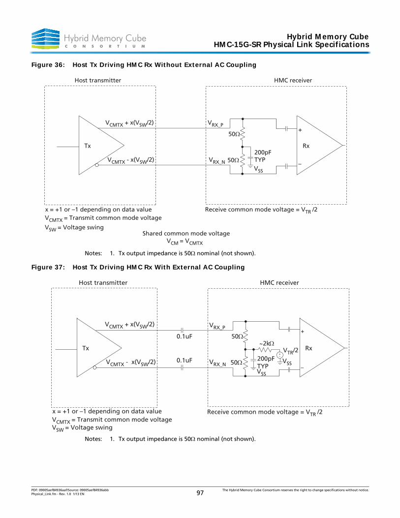
Hybrid Memory CubeHMC-15G-SR Physical Link Specifications
Figure 36: Host Tx Driving HMC Rx Without External AC Coupling
Notes: 1. Tx output impedance is 50 nominal (not shown).
Figure 37: Host Tx Driving HMC Rx With External AC Coupling
Notes: 1. Tx output impedance is 50 nominal (not shown).
50200pFTYP
50
VCMTX + x(VSW/2) VRX_P
VRX_NVSS
VCMTX - x(VSW/2)
Host transmitter HMC receiver
+
–
Rx
x = +1 or –1 depending on data valueVCMTX = Transmit common mode voltage
Shared common mode voltageVCM = VCMTX
Receive common mode voltage = VTR /2
Tx
VSW = Voltage swing
50
~2k0.1uF
0.1uF 200pFTYP
50
VTR/2
VSS
VSS
VCMTX + x(VSW/2)
VCMTX - x(VSW/2)
Host transmitter HMC receiver
+
–
+–
Rx
x = +1 or –1 depending on data valueVCMTX = Transmit common mode voltage
Receive common mode voltage = VTR /2
Tx
VSW = Voltage swing
VRX_P
VRX_N
PDF: 09005aef84936aaf/Source: 09005aef84936abb The Hybrid Memory Cube Consortium reserves the right to change specifications without notice.Physical_Link.fm - Rev. 1.0 1/13 EN 97
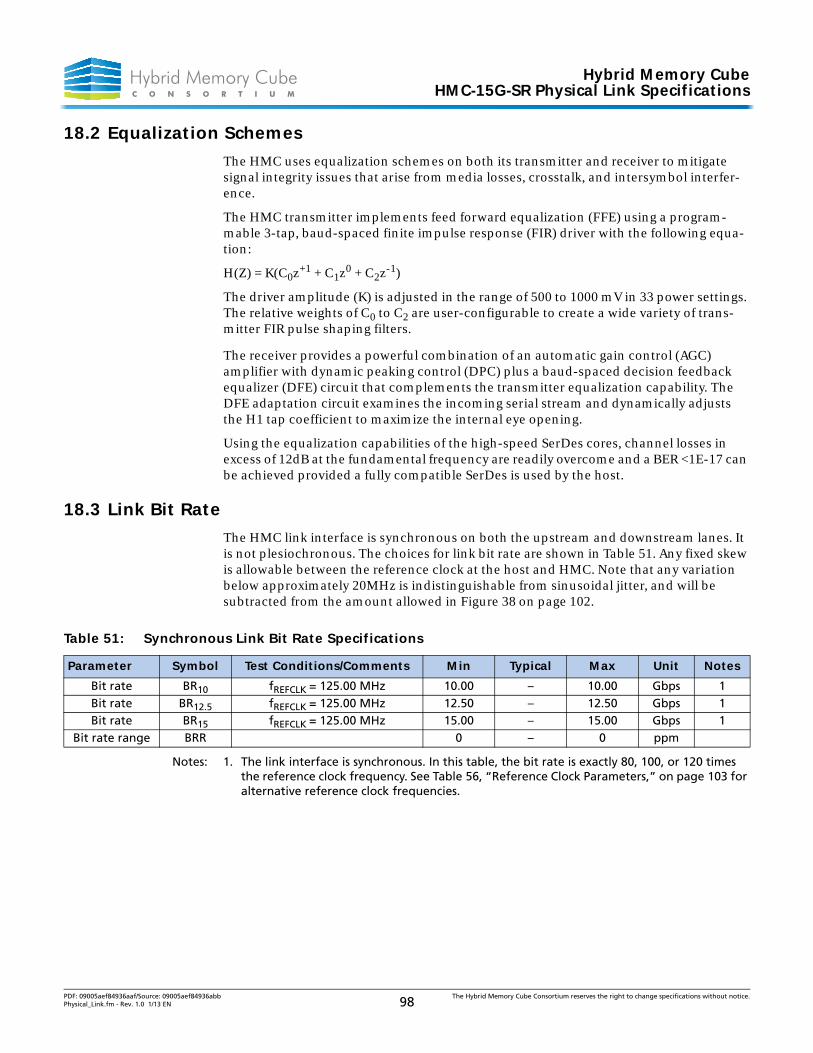
Hybrid Memory CubeHMC-15G-SR Physical Link Specifications
18.2 Equalization Schemes
The HMC uses equalization schemes on both its transmitter and receiver to mitigate signal integrity issues that arise from media losses, crosstalk, and intersymbol interfer-ence.
The HMC transmitter implements feed forward equalization (FFE) using a program-mable 3-tap, baud-spaced finite impulse response (FIR) driver with the following equa-tion:
H(Z) = K(C0z+1 + C1z0 + C2z-1)
The driver amplitude (K) is adjusted in the range of 500 to 1000 mV in 33 power settings. The relative weights of C0 to C2 are user-configurable to create a wide variety of trans-mitter FIR pulse shaping filters.
The receiver provides a powerful combination of an automatic gain control (AGC) amplifier with dynamic peaking control (DPC) plus a baud-spaced decision feedback equalizer (DFE) circuit that complements the transmitter equalization capability. The DFE adaptation circuit examines the incoming serial stream and dynamically adjusts the H1 tap coefficient to maximize the internal eye opening.
Using the equalization capabilities of the high-speed SerDes cores, channel losses in excess of 12dB at the fundamental frequency are readily overcome and a BER <1E-17 can be achieved provided a fully compatible SerDes is used by the host.
18.3 Link Bit Rate
The HMC link interface is synchronous on both the upstream and downstream lanes. It is not plesiochronous. The choices for link bit rate are shown in Table 51. Any fixed skew is allowable between the reference clock at the host and HMC. Note that any variation below approximately 20MHz is indistinguishable from sinusoidal jitter, and will be subtracted from the amount allowed in Figure 38 on page 102.
Notes: 1. The link interface is synchronous. In this table, the bit rate is exactly 80, 100, or 120 times the reference clock frequency. See Table 56, “Reference Clock Parameters,” on page 103 for alternative reference clock frequencies.
Table 51: Synchronous Link Bit Rate Specifications
Parameter Symbol Test Conditions/Comments Min Typical Max Unit Notes
Bit rate BR10 fREFCLK = 125.00 MHz 10.00 – 10.00 Gbps 1Bit rate BR12.5 fREFCLK = 125.00 MHz 12.50 – 12.50 Gbps 1Bit rate BR15 fREFCLK = 125.00 MHz 15.00 – 15.00 Gbps 1
Bit rate range BRR 0 – 0 ppm
PDF: 09005aef84936aaf/Source: 09005aef84936abb The Hybrid Memory Cube Consortium reserves the right to change specifications without notice.Physical_Link.fm - Rev. 1.0 1/13 EN 98
Hybrid Memory CubeHMC-15G-SR Physical Link Specifications
18.4 High Speed Signaling Parameters
All parameters within Table 52 and Table 53 represent those of the HMC. Host trans-mitter and receiver termination and signaling parameters may differ from those of the HMC as long as the parameters within the tables are still met for the HMC.
Table 52: TX Signaling Parameters
Parameter SymbolTest Conditions /
Comments Min Typical Max Unit Notes
Link supply Tx termination voltage
VTT 1.2 V ±0.06V 1.14 1.2 1.26 V
Differential peak-to-peak output voltage
VDIFF_TX
SMALL_SWING
VDIFF_TX = 2 × | VTX_P – VTX_N |Measured with slow square
wave (64 zeros followed by 64 ones) with ideal 100floating differential
termination
430mV – mVPP 1
VDIFF_TX
LARGE_SWING
860mV 1.1 × VTT mVPP 2
Single-ended voltage (with respect to VSS) on VTX_P, VTX_N
VTX_SE Active mode 0.2 × VTT
0.8 × VTT
mV
Down or sleep mode output voltage
VTX_PD High-Z mV 3
DC common mode output voltage
VTX_CM VTX_CM = DC(avg) of | VTX_P + VTX_N |
See Note 4
mV 4
AC common mode noise VTX_CM_NZ
SQUARE WAVE
1000mV differential peak-to-peak slow square wave
output amplitude
50 mVPP
VTX_CM_NZ
PRBS
PRBS data pattern 15 mVTMS
Short circuit current ISHORT_TX Output pins shorted to GND or each other
–50 50 mA
Differential Tx output rise/fall time
tTX_RISE, tTX_FALL
Measured from 20% to 80% into ideal 100load
18 ps
Differential transmitter resistance
ROD 80 100 120 5
Single-ended transmitter resistance
ROSE 40 50 60 5
Single-ended transmitter termination mismatch
RTX_DELTA_AC AC-coupled or DC-coupled (VHRX = VTT ± 50mV);Measured within a
differential pair
5 %
RTX_DELTA_DC DC-coupled (VTT - 200mV < VHRX <VTT - 100mV );Measured within a
differential pair
25 % 6, 7
PDF: 09005aef84936aaf/Source: 09005aef84936abb The Hybrid Memory Cube Consortium reserves the right to change specifications without notice.Physical_Link.fm - Rev. 1.0 1/13 EN 99
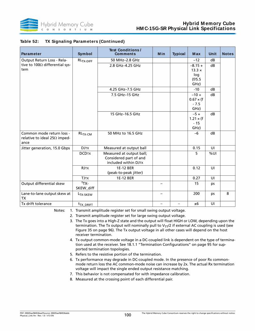
Hybrid Memory CubeHMC-15G-SR Physical Link Specifications
Notes: 1. Transmit amplitude register set for small swing output voltage.2. Transmit amplitude register set for large swing output voltage.3. The Tx goes into a High-Z state and the output will float HIGH or LOW, depending upon the
termination. The Tx output will nominally pull to VTT/2 if external AC coupling is used (see Figure 35 on page 96). The Tx output voltage in all other cases will depend on the host receiver termination.
4. Tx output common-mode voltage in a DC-coupled link is dependent on the type of termina-tion used at the receiver. See 18.1.1 “Termination Configurations” on page 95 for sup-ported termination topologies.
5. Refers to the resistive portion of the termination.6. Tx performance may degrade in DC-coupled mode. In the presence of poor Rx common-
mode return loss the AC common-mode noise can increase by 2x. The actual Rx termination voltage will impact the single ended output resistance matching.
7. This behavior is not compensated for with impedance calibration.8. Measured at the crossing point of each differential pair.
Output Return Loss - Rela-tive to 100 differential sys-tem
RLTX-DIFF 50 MHz–2.8 GHz –12 dB2.8 GHz–4.25 GHz –8.15 +
13.3 × log
(f/5.5 GHz)
dB
4.25 GHz–7.5 GHz -10 dB7.5 GHz–15 GHz –10 +
0.67 × (f - 7.5 GHz)
dB
15 GHz–16.5 GHz –5 + 1.21 × (f
- 15 GHz)
dB
Common mode return loss - relative to ideal 25 imped-ance
RLTX-CM 50 MHz to 16.5 GHz –6 dB
Jitter generation, 15.0 Gbps DJTX Measured at output ball 0.15 UIDCDTX Measured at output ball;
Considered part of and included within DJTX
5 %UI
RJTX 1E-12 BER(peak-to-peak jitter)
0.12 UI
TJTX 1E-12 BER 0.27 UIOutput differential skew tTX-
SKEW_diff– 15 ps
Lane-to-lane output skew at TX
LTX-SKEW – 200 ps 8
Tx drift tolerance tTX_DRIFT – – ±6 UI
Table 52: TX Signaling Parameters (Continued)
Parameter SymbolTest Conditions /
Comments Min Typical Max Unit Notes
PDF: 09005aef84936aaf/Source: 09005aef84936abb The Hybrid Memory Cube Consortium reserves the right to change specifications without notice.Physical_Link.fm - Rev. 1.0 1/13 EN 100
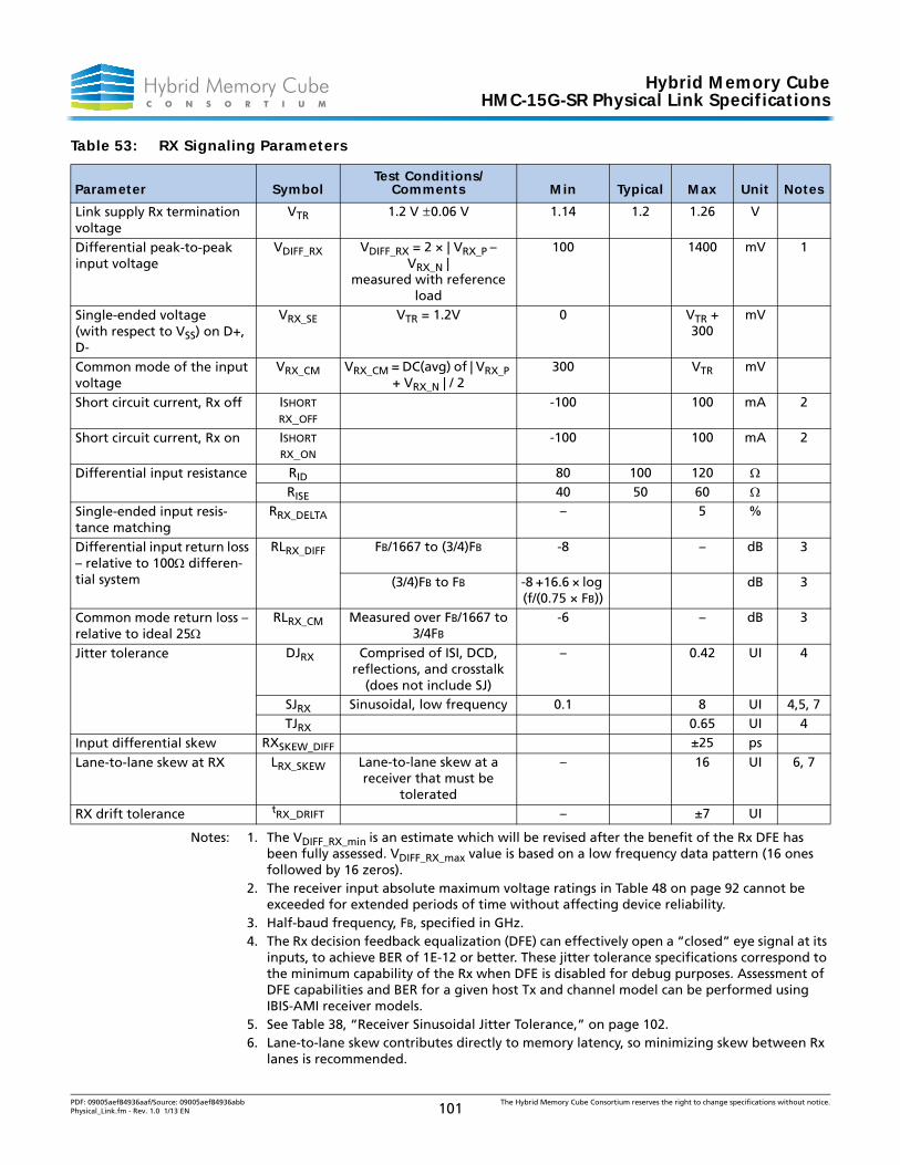
Hybrid Memory CubeHMC-15G-SR Physical Link Specifications
Notes: 1. The VDIFF_RX_min is an estimate which will be revised after the benefit of the Rx DFE has been fully assessed. VDIFF_RX_max value is based on a low frequency data pattern (16 ones followed by 16 zeros).
2. The receiver input absolute maximum voltage ratings in Table 48 on page 92 cannot be exceeded for extended periods of time without affecting device reliability.
3. Half-baud frequency, FB, specified in GHz.4. The Rx decision feedback equalization (DFE) can effectively open a “closed” eye signal at its
inputs, to achieve BER of 1E-12 or better. These jitter tolerance specifications correspond to the minimum capability of the Rx when DFE is disabled for debug purposes. Assessment of DFE capabilities and BER for a given host Tx and channel model can be performed using IBIS-AMI receiver models.
5. See Table 38, “Receiver Sinusoidal Jitter Tolerance,” on page 102.6. Lane-to-lane skew contributes directly to memory latency, so minimizing skew between Rx
lanes is recommended.
Table 53: RX Signaling Parameters
Parameter SymbolTest Conditions/
Comments Min Typical Max Unit Notes
Link supply Rx termination voltage
VTR 1.2 V ±0.06 V 1.14 1.2 1.26 V
Differential peak-to-peak input voltage
VDIFF_RX VDIFF_RX = 2 × | VRX_P – VRX_N |
measured with reference load
100 1400 mV 1
Single-ended voltage(with respect to VSS) on D+, D-
VRX_SE VTR = 1.2V 0 VTR + 300
mV
Common mode of the input voltage
VRX_CM VRX_CM = DC(avg) of | VRX_P + VRX_N | / 2
300 VTR mV
Short circuit current, Rx off ISHORT
RX_OFF
-100 100 mA 2
Short circuit current, Rx on ISHORT
RX_ON
-100 100 mA 2
Differential input resistance RID 80 100 120 RISE 40 50 60
Single-ended input resis-tance matching
RRX_DELTA – 5 %
Differential input return loss – relative to 100 differen-tial system
RLRX_DIFF FB/1667 to (3/4)FB -8 – dB 3
(3/4)FB to FB -8 +16.6 × log (f/(0.75 × FB))
dB 3
Common mode return loss – relative to ideal 25
RLRX_CM Measured over FB/1667 to 3/4FB
-6 – dB 3
Jitter tolerance DJRX Comprised of ISI, DCD, reflections, and crosstalk
(does not include SJ)
– 0.42 UI 4
SJRX Sinusoidal, low frequency 0.1 8 UI 4,5, 7TJRX 0.65 UI 4
Input differential skew RXSKEW_DIFF ±25 ps
Lane-to-lane skew at RX LRX_SKEW Lane-to-lane skew at a receiver that must be
tolerated
– 16 UI 6, 7
RX drift tolerance tRX_DRIFT – ±7 UI
PDF: 09005aef84936aaf/Source: 09005aef84936abb The Hybrid Memory Cube Consortium reserves the right to change specifications without notice.Physical_Link.fm - Rev. 1.0 1/13 EN 101
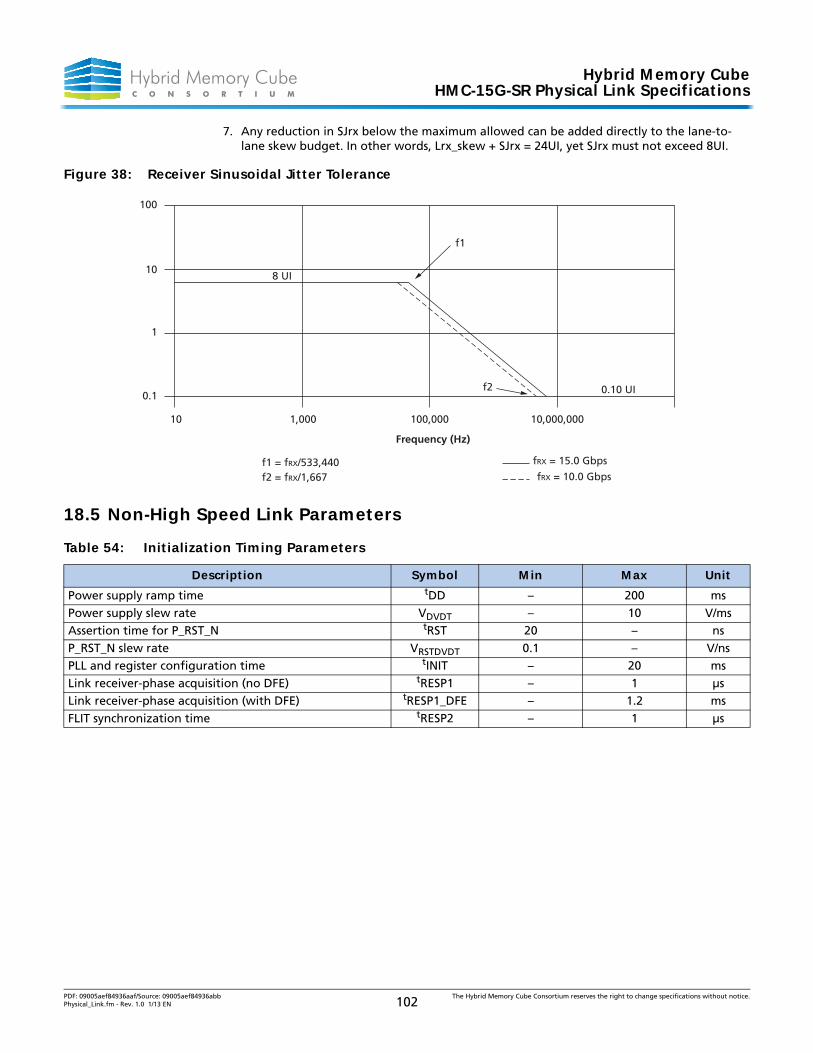
Hybrid Memory CubeHMC-15G-SR Physical Link Specifications
7. Any reduction in SJrx below the maximum allowed can be added directly to the lane-to-lane skew budget. In other words, Lrx_skew + SJrx = 24UI, yet SJrx must not exceed 8UI.
Figure 38: Receiver Sinusoidal Jitter Tolerance
18.5 Non-High Speed Link Parameters
Table 54: Initialization Timing Parameters
Description Symbol Min Max Unit
Power supply ramp time tDD – 200 msPower supply slew rate VDVDT – 10 V/msAssertion time for P_RST_N tRST 20 – nsP_RST_N slew rate VRSTDVDT 0.1 – V/nsPLL and register configuration time tINIT – 20 msLink receiver-phase acquisition (no DFE) tRESP1 – 1 µsLink receiver-phase acquisition (with DFE) tRESP1_DFE – 1.2 msFLIT synchronization time tRESP2 – 1 µs
f1
f1 = fRX/533,440 fRX = 15.0 Gbps
fRX = 10.0 Gbps
Frequency (Hz)
f2 = fRX/1,667
f2 0.10 UI
8 UI
10
0.1
1
10
100
1,000 100,000 10,000,000
PDF: 09005aef84936aaf/Source: 09005aef84936abb The Hybrid Memory Cube Consortium reserves the right to change specifications without notice.Physical_Link.fm - Rev. 1.0 1/13 EN 102
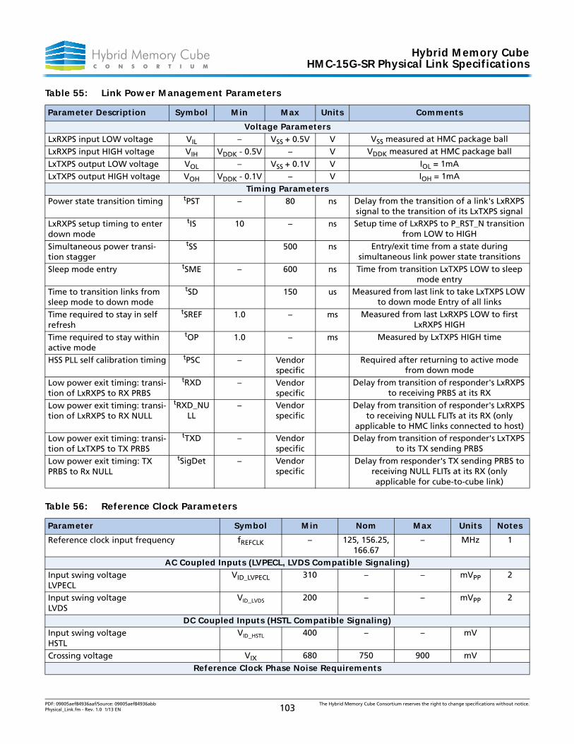
Hybrid Memory CubeHMC-15G-SR Physical Link Specifications
Table 55: Link Power Management Parameters
Parameter Description Symbol Min Max Units Comments
Voltage ParametersLxRXPS input LOW voltage VIL – VSS + 0.5V V VSS measured at HMC package ball
LxRXPS input HIGH voltage VIH VDDK - 0.5V – V VDDK measured at HMC package ball
LxTXPS output LOW voltage VOL – VSS + 0.1V V IOL = 1mA
LxTXPS output HIGH voltage VOH VDDK - 0.1V – V IOH = 1mA
Timing ParametersPower state transition timing tPST – 80 ns Delay from the transition of a link's LxRXPS
signal to the transition of its LxTXPS signalLxRXPS setup timing to enter down mode
tIS 10 – ns Setup time of LxRXPS to P_RST_N transition from LOW to HIGH
Simultaneous power transi-tion stagger
tSS 500 ns Entry/exit time from a state during simultaneous link power state transitions
Sleep mode entry tSME – 600 ns Time from transition LxTXPS LOW to sleep mode entry
Time to transition links from sleep mode to down mode
tSD 150 us Measured from last link to take LxTXPS LOW to down mode Entry of all links
Time required to stay in self refresh
tSREF 1.0 – ms Measured from last LxRXPS LOW to first LxRXPS HIGH
Time required to stay within active mode
tOP 1.0 – ms Measured by LxTXPS HIGH time
HSS PLL self calibration timing tPSC – Vendor specific
Required after returning to active mode from down mode
Low power exit timing: transi-tion of LxRXPS to RX PRBS
tRXD – Vendor specific
Delay from transition of responder's LxRXPS to receiving PRBS at its RX
Low power exit timing: transi-tion of LxRXPS to RX NULL
tRXD_NULL
– Vendor specific
Delay from transition of responder's LxRXPS to receiving NULL FLITs at its RX (only
applicable to HMC links connected to host)Low power exit timing: transi-tion of LxTXPS to TX PRBS
tTXD – Vendor specific
Delay from transition of responder's LxTXPS to its TX sending PRBS
Low power exit timing: TX PRBS to Rx NULL
tSigDet – Vendor specific
Delay from responder's TX sending PRBS to receiving NULL FLITs at its RX (only applicable for cube-to-cube link)
Table 56: Reference Clock Parameters
Parameter Symbol Min Nom Max Units Notes
Reference clock input frequency fREFCLK – 125, 156.25, 166.67
– MHz 1
AC Coupled Inputs (LVPECL, LVDS Compatible Signaling)Input swing voltageLVPECL
VID_LVPECL 310 – – mVPP 2
Input swing voltageLVDS
VID_LVDS 200 – – mVPP 2
DC Coupled Inputs (HSTL Compatible Signaling)Input swing voltageHSTL
VID_HSTL 400 – – mV
Crossing voltage VIX 680 750 900 mV
Reference Clock Phase Noise Requirements
PDF: 09005aef84936aaf/Source: 09005aef84936abb The Hybrid Memory Cube Consortium reserves the right to change specifications without notice.Physical_Link.fm - Rev. 1.0 1/13 EN 103
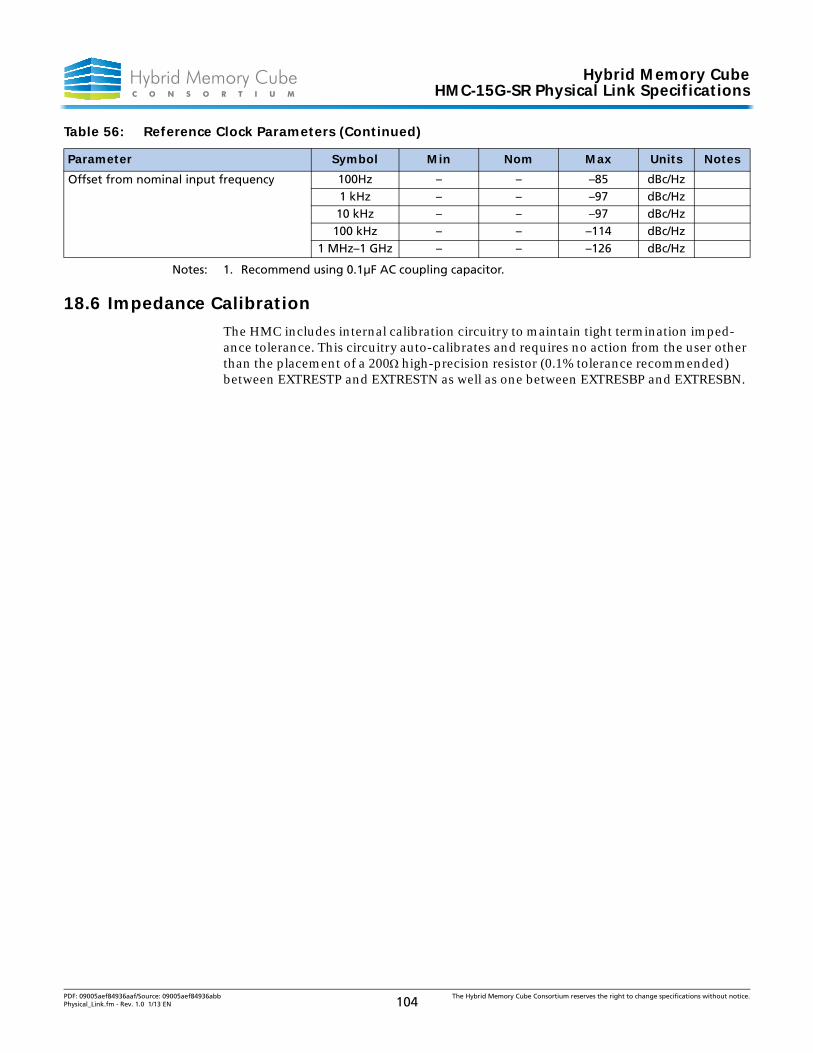
Hybrid Memory CubeHMC-15G-SR Physical Link Specifications
Notes: 1. Recommend using 0.1µF AC coupling capacitor.
18.6 Impedance Calibration
The HMC includes internal calibration circuitry to maintain tight termination imped-ance tolerance. This circuitry auto-calibrates and requires no action from the user other than the placement of a 200high-precision resistor (0.1% tolerance recommended) between EXTRESTP and EXTRESTN as well as one between EXTRESBP and EXTRESBN.
Offset from nominal input frequency 100Hz – – –85 dBc/Hz1 kHz – – –97 dBc/Hz10 kHz – – –97 dBc/Hz
100 kHz – – –114 dBc/Hz1 MHz–1 GHz – – –126 dBc/Hz
Table 56: Reference Clock Parameters (Continued)
Parameter Symbol Min Nom Max Units Notes
PDF: 09005aef84936aaf/Source: 09005aef84936abb The Hybrid Memory Cube Consortium reserves the right to change specifications without notice.Physical_Link.fm - Rev. 1.0 1/13 EN 104
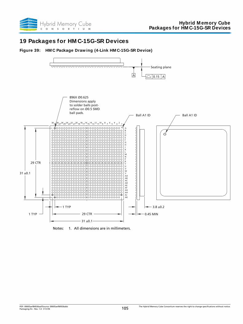
Hybrid Memory CubePackages for HMC-15G-SR Devices
19 Packages for HMC-15G-SR Devices
Figure 39: HMC Package Drawing (4-Link HMC-15G-SR Device)
Notes: 1. All dimensions are in millimeters.
0.45 MIN
3.8 ±0.2
29 CTR
31 ±0.1
1 TYP
31 ±0.1
Ball A1 IDBall A1 ID
Seating plane
0.15 AA
896X Ø0.625Dimensions applyto solder balls post-reflow on Ø0.5 SMDball pads.
29 CTR
1 TYP
12
34
56
78
910
111214
15171820
212322
1916
13
ABCDEFGHJKLMNPRTUVWYAAABACADAEAFAGAHAJAK
2425
2627
2829
30
PDF: 09005aef84936aaf/Source: 09005aef84936abb The Hybrid Memory Cube Consortium reserves the right to change specifications without notice.Packaging.fm - Rev. 1.0 1/13 EN 105
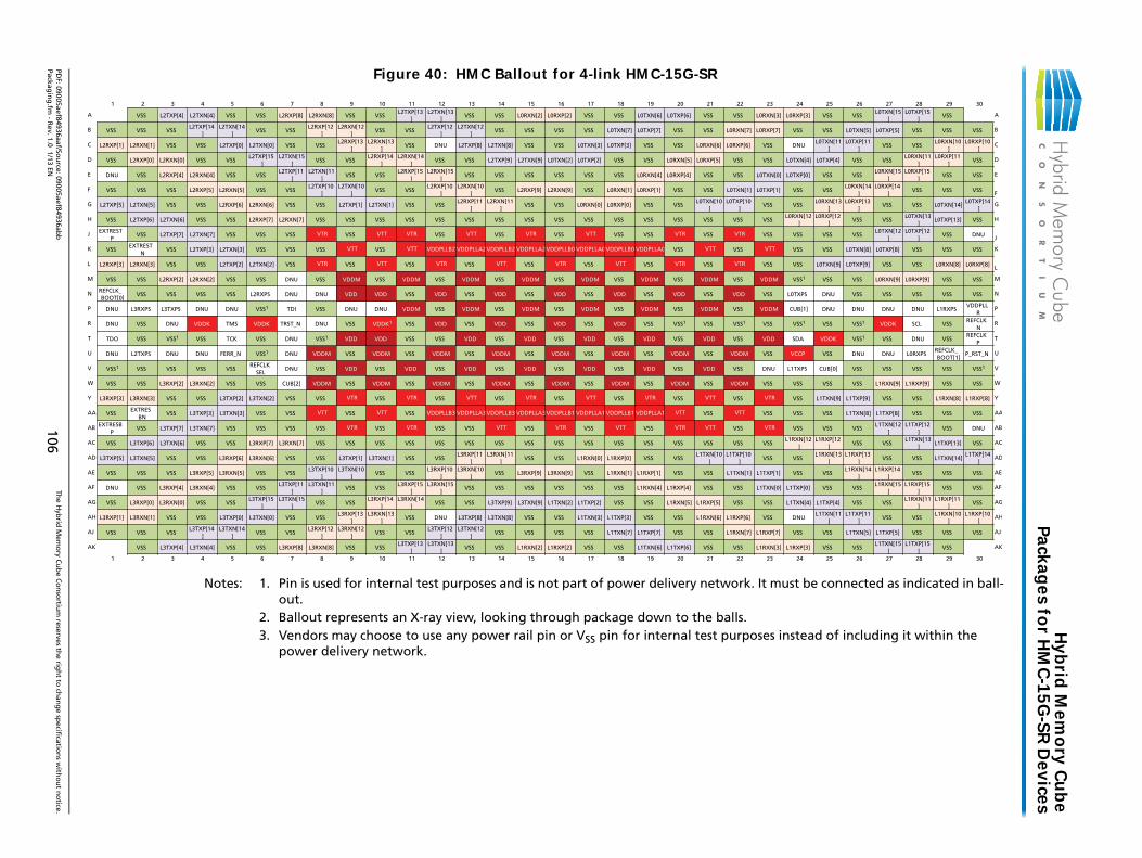
Hyb
rid M
emo
ry Cu
be
Packages fo
r HM
C-15G
-SR D
evices
PDF: 09005aef849
Packagin
g.fm
-R
ev. 1.0 1/13 EN106
Figure 40: HMC Ballout for 4-link HMC-15G-SR
onnected as indicated in ball-
f including it within the
1 2 3 4 5 6 7 8 9 10 11 12 13 14 15 16 17 18 19 20 21 22 23 24 25 26 27 28 29 30
A VSS L2TXP[4] L2TXN[4] VSS VSS L2RXP[8] L2RXN[8] VSS VSSL2TXP[13
]L2TXN[13
]VSS VSS L0RXN[2] L0RXP[2] VSS VSS L0TXN[6] L0TXP[6] VSS VSS L0RXN[3] L0RXP[3] VSS VSS
L0TXN[15]
L0TXP[15]
VSS A
S L0TXN[5] L0TXP[5] VSS VSS VSS B
N[11]
L0TXP[11]
VSS VSSL0RXN[10
]L0RXP[10
]C
P[4] VSS VSSL0RXN[11
]L0RXP[11
]VSS D
S VSSL0RXN[15
]L0RXP[15
]VSS VSS E
SL0RXN[14
]L0RXP[14
]VSS VSS VSS F
N[13]
L0RXP[13]
VSS VSS L0TXN[14]L0TXP[14
]G
P[12]
VSS VSSL0TXN[13
]L0TXP[13] VSS H
S VSSL0TXN[12
]L0TXP[12
]VSS DNU J
S L0TXN[8] L0TXP[8] VSS VSS VSS K
N[9] L0TXP[9] VSS VSS L0RXN[8] L0RXP[8] L
S VSS L0RXN[9] L0RXP[9] VSS VSS M
U VSS VSS VSS VSS VSS N
U DNU DNU DNU L1RXPSVDDPLL
RP
S VSS1 VDDK SCL VSSREFCLK
NR
DK VSS1 VSS DNU VSSREFCLK
PT
S DNU DNU L0RXPSREFCLK_BOOT[1]
P_RST_N U
B[0] VSS VSS VSS VSS VSS1 V
S VSS L1RXN[9] L1RXP[9] VSS VSS W
N[9] L1TXP[9] VSS VSS L1RXN[8] L1RXP[8] Y
S L1TXN[8] L1TXP[8] VSS VSS VSS AA
S VSSL1TXN[12
]L1TXP[12
]VSS DNU AB
P[12]
VSS VSSL1TXN[13
]L1TXP[13] VSS AC
N[13]
L1RXP[13]
VSS VSS L1TXN[14]L1TXP[14
]AD
SL1RXN[14
]L1RXP[14
]VSS VSS VSS AE
S VSSL1RXN[15
]L1RXP[15
]VSS VSS AF
P[4] VSS VSSL1RXN[11
]L1RXP[11
]VSS AG
N[11]
L1TXP[11]
VSS VSSL1RXN[10
]L1RXP[10
]AH
S L1TXN[5] L1TXP[5] VSS VSS VSS AJ
S VSSL1TXN[15
]L1TXP[15
]VSS AK
5 26 27 28 29 30
36aaf/Sou
rce: 09005aef84936abb
The H
ybrid
Mem
ory C
ub
e Co
nso
rtium
reserves the rig
ht to
chan
ge sp
ecification
s with
ou
t no
tice.
Notes: 1. Pin is used for internal test purposes and is not part of power delivery network. It must be cout.
2. Ballout represents an X-ray view, looking through package down to the balls.3. Vendors may choose to use any power rail pin or VSS pin for internal test purposes instead o
power delivery network.
B VSS VSS VSSL2TXP[14
]L2TXN[14
]VSS VSS
L2RXP[12]
L2RXN[12]
VSS VSSL2TXP[12
]L2TXN[12
]VSS VSS VSS VSS L0TXN[7] L0TXP[7] VSS VSS L0RXN[7] L0RXP[7] VSS VS
C L2RXP[1] L2RXN[1] VSS VSS L2TXP[0] L2TXN[0] VSS VSSL2RXP[13
]L2RXN[13
]VSS DNU L2TXP[8] L2TXN[8] VSS VSS L0TXN[3] L0TXP[3] VSS VSS L0RXN[6] L0RXP[6] VSS DNU
L0TX
D VSS L2RXP[0] L2RXN[0] VSS VSSL2TXP[15
]L2TXN[15
]VSS VSS
L2RXP[14]
L2RXN[14]
VSS VSS L2TXP[9] L2TXN[9] L0TXN[2] L0TXP[2] VSS VSS L0RXN[5] L0RXP[5] VSS VSS L0TXN[4] L0TX
E DNU VSS L2RXP[4] L2RXN[4] VSS VSSL2TXP[11
]L2TXN[11
]VSS VSS
L2RXP[15]
L2RXN[15]
VSS VSS VSS VSS VSS VSS L0RXN[4] L0RXP[4] VSS VSS L0TXN[0] L0TXP[0] VS
F VSS VSS VSS L2RXP[5] L2RXN[5] VSS VSSL2TXP[10
]L2TXN[10
]VSS VSS
L2RXP[10]
L2RXN[10]
VSS L2RXP[9] L2RXN[9] VSS L0RXN[1] L0RXP[1] VSS VSS L0TXN[1] L0TXP[1] VSS VS
G L2TXP[5] L2TXN[5] VSS VSS L2RXP[6] L2RXN[6] VSS VSS L2TXP[1] L2TXN[1] VSS VSSL2RXP[11
]L2RXN[11
]VSS VSS L0RXN[0] L0RXP[0] VSS VSS
L0TXN[10]
L0TXP[10]
VSS VSSL0RX
H VSS L2TXP[6] L2TXN[6] VSS VSS L2RXP[7] L2RXN[7] VSS VSS VSS VSS VSS VSS VSS VSS VSS VSS VSS VSS VSS VSS VSS VSSL0RXN[12
]L0RX
J EXTRESTP
VSS L2TXP[7] L2TXN[7] VSS VSS VSS VTR VSS VTT VTR VSS VTT VSS VTR VSS VTT VSS VSS VTR VSS VTR VSS VSS VS
K VSSEXTREST
NVSS L2TXP[3] L2TXN[3] VSS VSS VSS VTT VSS VTT VDDPLLB2 VDDPLLA2VDDPLLB2 VDDPLLA2VDDPLLB0 VDDPLLA0VDDPLLB0 VDDPLLA0 VSS VTT VSS VTT VSS VS
L L2RXP[3] L2RXN[3] VSS VSS L2TXP[2] L2TXN[2] VSS VTR VSS VTT VSS VTR VSS VTT VSS VTR VSS VTT VSS VTR VSS VTR VSS VSS L0TX
M VSS VSS L2RXP[2] L2RXN[2] VSS VSS DNU VSS VDDM VSS VDDM VSS VDDM VSS VDDM VSS VDDM VSS VDDM VSS VDDM VSS VDDM VSS1 VS
N REFCLK_BOOT[0]
VSS VSS VSS VSS L2RXPS DNU DNU VDD VDD VSS VDD VSS VDD VSS VDD VSS VDD VSS VDD VSS VDD VSS L0TXPS DN
P DNU L3RXPS L3TXPS DNU DNU VSS1 TDI VSS DNU DNU VDDM VSS VDDM VSS VDDM VSS VDDM VSS VDDM VSS VDDM VSS VDDM CUB[1] DN
R DNU VSS DNU VDDK TMS VDDK TRST_N DNU VSS VDDK1 VSS VDD VSS VDD VSS VDD VSS VDD VSS VSS1 VSS VSS1 VSS VSS1 VS
T TDO VSS VSS1 VSS TCK VSS DNU VSS1 VDD VDD VSS VSS VDD VSS VDD VSS VDD VSS VDD VSS VDD VSS VDD SDA VD
U DNU L2TXPS DNU DNU FERR_N VSS1 DNU VDDM VSS VDDM VSS VDDM VSS VDDM VSS VDDM VSS VDDM VSS VDDM VSS VDDM VSS VCCP VS
V VSS1 VSS VSS VSS VSSREFCLK
SELDNU VSS VDD VSS VDD VSS VDD VSS VDD VSS VDD VSS VDD VSS VDD VSS DNU L1TXPS CU
W VSS VSS L3RXP[2] L3RXN[2] VSS VSS CUB[2] VDDM VSS VDDM VSS VDDM VSS VDDM VSS VDDM VSS VDDM VSS VDDM VSS VDDM VSS VSS VS
Y L3RXP[3] L3RXN[3] VSS VSS L3TXP[2] L3TXN[2] VSS VSS VTR VSS VTR VSS VTT VSS VTR VSS VTT VSS VTR VSS VTT VSS VTR VSS L1TX
AA VSSEXTRES
BNVSS L3TXP[3] L3TXN[3] VSS VSS VTT VSS VTT VSS VDDPLLB3 VDDPLLA3VDDPLLB3 VDDPLLA3VDDPLLB1 VDDPLLA1VDDPLLB1 VDDPLLA1 VTT VSS VTT VSS VSS VS
AB EXTRESBP
VSS L3TXP[7] L3TXN[7] VSS VSS VSS VSS VTR VSS VTR VSS VSS VTT VSS VTR VSS VTT VSS VTR VTT VSS VTR VSS VS
AC VSS L3TXP[6] L3TXN[6] VSS VSS L3RXP[7] L3RXN[7] VSS VSS VSS VSS VSS VSS VSS VSS VSS VSS VSS VSS VSS VSS VSS VSSL1RXN[12
]L1RX
AD L3TXP[5] L3TXN[5] VSS VSS L3RXP[6] L3RXN[6] VSS VSS L3TXP[1] L3TXN[1] VSS VSSL3RXP[11
]L3RXN[11
]VSS VSS L1RXN[0] L1RXP[0] VSS VSS
L1TXN[10]
L1TXP[10]
VSS VSSL1RX
AE VSS VSS VSS L3RXP[5] L3RXN[5] VSS VSSL3TXP[10
]L3TXN[10
]VSS VSS
L3RXP[10]
L3RXN[10]
VSS L3RXP[9] L3RXN[9] VSS L1RXN[1] L1RXP[1] VSS VSS L1TXN[1] L1TXP[1] VSS VS
AF DNU VSS L3RXP[4] L3RXN[4] VSS VSSL3TXP[11
]L3TXN[11
]VSS VSS
L3RXP[15]
L3RXN[15]
VSS VSS VSS VSS VSS VSS L1RXN[4] L1RXP[4] VSS VSS L1TXN[0] L1TXP[0] VS
AG VSS L3RXP[0] L3RXN[0] VSS VSSL3TXP[15
]L3TXN[15
]VSS VSS
L3RXP[14]
L3RXN[14]
VSS VSS L3TXP[9] L3TXN[9] L1TXN[2] L1TXP[2] VSS VSS L1RXN[5] L1RXP[5] VSS VSS L1TXN[4] L1TX
AH L3RXP[1] L3RXN[1] VSS VSS L3TXP[0] L3TXN[0] VSS VSSL3RXP[13
]L3RXN[13
]VSS DNU L3TXP[8] L3TXN[8] VSS VSS L1TXN[3] L1TXP[3] VSS VSS L1RXN[6] L1RXP[6] VSS DNU
L1TX
AJ VSS VSS VSSL3TXP[14
]L3TXN[14
]VSS VSS
L3RXP[12]
L3RXN[12]
VSS VSSL3TXP[12
]L3TXN[12
]VSS VSS VSS VSS L1TXN[7] L1TXP[7] VSS VSS L1RXN[7] L1RXP[7] VSS VS
AK VSS L3TXP[4] L3TXN[4] VSS VSS L3RXP[8] L3RXN[8] VSS VSSL3TXP[13
]L3TXN[13
]VSS VSS L1RXN[2] L1RXP[2] VSS VSS L1TXN[6] L1TXP[6] VSS VSS L1RXN[3] L1RXP[3] VS
1 2 3 4 5 6 7 8 9 10 11 12 13 14 15 16 17 18 19 20 21 22 23 24 2
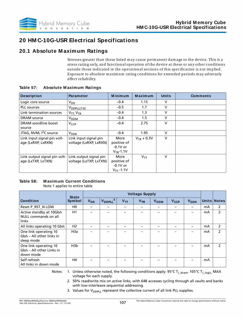
Hybrid Memory CubeHMC-10G-USR Electrical Specifications
20 HMC-10G-USR Electrical Specifications
20.1 Absolute Maximum Ratings
Stresses greater than those listed may cause permanent damage to the device. This is a stress rating only, and functional operation of the device at these or any other conditions outside those indicated in the operational sections of this specification is not implied. Exposure to absolute maximum rating conditions for extended periods may adversely affect reliability.
Notes: 1. Unless otherwise noted, the following conditions apply: 95°C TJ_dram, 105°C TJ_logic, MAX voltage for each supply.
2. 50% read/write mix on active links, with 64B accesses cycling through all vaults and banks with low-interleave sequential addressing.
3. Values for VDDPLL represent the collective current of all link PLL supplies.
Table 57: Absolute Maximum Ratings
Description Parameter Minimum Maximum Units Comments
Logic core source VDD –0.4 1.15 V
PLL sources VDDPLL[7:0] –0.5 1.7 V
Link termination sources VTT, VTR –0.4 1.3 V
DRAM source VDDM –0.4 1.5 V
DRAM wordline boost source
VCCP –0.4 2.75 V
JTAG, NVM, I2C source VDDK –0.4 1.95 V
Link input signal pin volt-age (LxRXP, LxRXN)
Link input signal pin voltage (LxRXP, LxRXN)
More positive of
-0.1V or VTR-1.1V
VTR + 0.3V V
Link output signal pin volt-age (LxTXP, LxTXN)
Link output signal pin voltage (LxTXP, LxTXN)
More positive of
-0.1V or VTT -1.1V
VTT V
Table 58: Maximum Current ConditionsNote 1 applies to entire table
ConditionState
Symbol
Voltage Supply
Units NotesVDD VDDPLL3 VTT VTR VDDM VCCP VDDK
Reset P_RST_N LOW H0 – – – – – – – mA 2
Active standby at 10Gb/sNULL commands on all links
H1 – – – – – – – mA 2
All links operating 10 Gb/s H2 – – – – – – – mA 2
One link operating 10 Gb/s – All other links in sleep mode
H3a – – – – – – – mA 2
One link operating 10 Gb/s – All other Links in down mode
H3b – – – – – – – mA 2
Self refreshAll links in down mode
H4 – – – – – – – mA
PDF: 09005aef84936aaf/Source: 09005aef84936abb The Hybrid Memory Cube Consortium reserves the right to change specifications without notice.10G-USR_Electrical_Specifications.fm - Rev. 1.0 1/13 EN 107
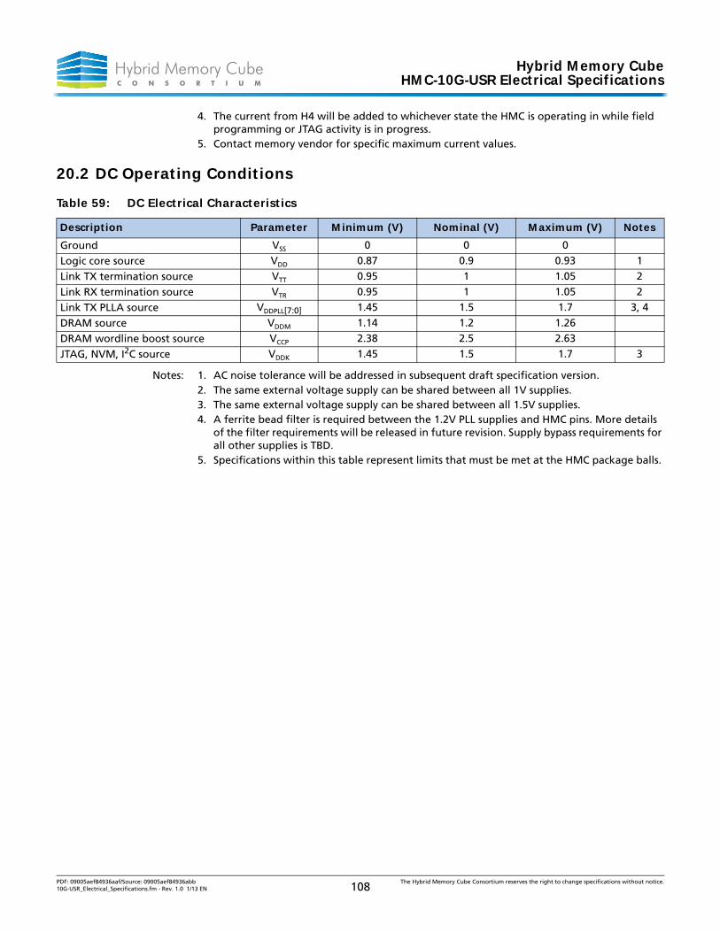
Hybrid Memory CubeHMC-10G-USR Electrical Specifications
4. The current from H4 will be added to whichever state the HMC is operating in while field programming or JTAG activity is in progress.
5. Contact memory vendor for specific maximum current values.
20.2 DC Operating Conditions
Notes: 1. AC noise tolerance will be addressed in subsequent draft specification version.2. The same external voltage supply can be shared between all 1V supplies.3. The same external voltage supply can be shared between all 1.5V supplies.4. A ferrite bead filter is required between the 1.2V PLL supplies and HMC pins. More details
of the filter requirements will be released in future revision. Supply bypass requirements for all other supplies is TBD.
5. Specifications within this table represent limits that must be met at the HMC package balls.
Table 59: DC Electrical Characteristics
Description Parameter Minimum (V) Nominal (V) Maximum (V) Notes
Ground VSS 0 0 0
Logic core source VDD 0.87 0.9 0.93 1
Link TX termination source VTT 0.95 1 1.05 2
Link RX termination source VTR 0.95 1 1.05 2
Link TX PLLA source VDDPLL[7:0] 1.45 1.5 1.7 3, 4
DRAM source VDDM 1.14 1.2 1.26
DRAM wordline boost source VCCP 2.38 2.5 2.63
JTAG, NVM, I2C source VDDK 1.45 1.5 1.7 3
PDF: 09005aef84936aaf/Source: 09005aef84936abb The Hybrid Memory Cube Consortium reserves the right to change specifications without notice.10G-USR_Electrical_Specifications.fm - Rev. 1.0 1/13 EN 108
Hybrid Memory CubeHMC-10G-USR Physical Link Specifications
21 HMC-10G-USR Physical Link Specifications
21.1 Physical Link Electrical Interface
The HMC transmitter and receiver circuits for the 10Gb/s USR physical link (PHY) are designed to be DC coupled to the host device. Both the HMC Rx and Tx circuits are meant to be connected to their respective host lanes through the use of 100 differential line impedance. Channel characteristics are expected to be “well-behaved” (to be more rigorously defined in the following sections) in order to support low-power (on the order of 1pJ/bit or 1mW/Gb/s) USR PHY circuitry. This places restrictions on the tolerable channel loss as well as lane-to-lane skew within a link.
Although the HMC-15G-SR physical link can operate at 10Gb/s, there is no intent for interoperability between the HMC-10G-USR and HMC-15G-SR physical links.
21.1.1 Termination Configuration
The impedance values shown are nominal. Host transmitter and receiver termination and signaling parameters may differ from those of the HMC as long as the HMC receiver parameters are still met per Table 61, “HMC-USR TX Signaling Parameters,” on page 112” and Table 63, “HMC-USR RX Signaling Parameters,” on page 116. The HMC has been designed to minimize the probability of long DC run lengths with its scram-bling and descrambling circuitry. Seeding values vary per lane, as described in more detail in “Scrambling and Descrambling” on page 15.
AC coupling of the HMC to the host device is not supported. In all lane connections, the transmitter must supply an appropriate common-mode level for DC compatibility with the receiver at the opposite end of the connection. The common-mode requirements are described in Table 61 and Table 63.
Figure 41 shows the HMC-USR transmitter driving a receiver in the host device. The HMC-USR transmitter has adjustable transmit swing controlled through bias current IDRIV. This current is 3b controllable with 50mVppd launch amplitude steps, for a maximum launch amplitude of 400mVppd, as specified in Table 61. During startup cali-bration, the launch amplitude is adjusted such that the lane can run at a target BER (1E-12, 1E-14, or 1E-16) programmed by the user, while providing sufficient voltage margin to guard against power supply fluctuations. Alternatively, the value of IDRIV can be programmed through the JTAG interface. Common-mode resistor RCM sets the trans-mitter common-mode level roughly equal to VTT/4. Capacitor CTT ensures proper common-mode return loss as specified in Table 61. Capacitance values for CTT will vary among HMC vendors, but it is recommended that this value be in the range of 25–35pF.
PDF: 09005aef84936aaf/Source: 09005aef84936abb The Hybrid Memory Cube Consortium reserves the right to change specifications without notice.10G-USR_Physical_Link_Specifications.fm - Rev. 1.0 1/13 EN 109
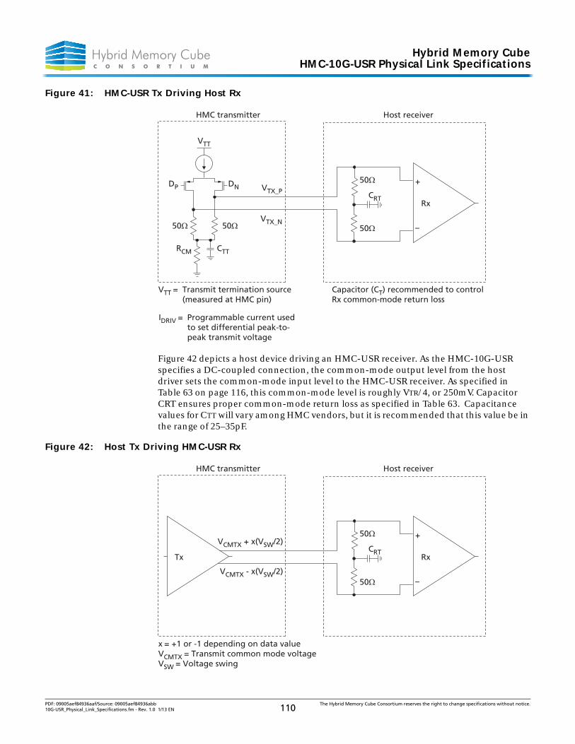
Hybrid Memory CubeHMC-10G-USR Physical Link Specifications
Figure 41: HMC-USR Tx Driving Host Rx
Figure 42 depicts a host device driving an HMC-USR receiver. As the HMC-10G-USR specifies a DC-coupled connection, the common-mode output level from the host driver sets the common-mode input level to the HMC-USR receiver. As specified in Table 63 on page 116, this common-mode level is roughly VTR/4, or 250mV. Capacitor CRT ensures proper common-mode return loss as specified in Table 63. Capacitance values for CTT will vary among HMC vendors, but it is recommended that this value be in the range of 25–35pF.
Figure 42: Host Tx Driving HMC-USR Rx
HMC transmitter Host receiver
VTX_P
VTX_N
VTT
DP DN
RCM CTT
VTT = Transmit termination source (measured at HMC pin)
Capacitor (CT) recommended to controlRx common-mode return loss
IDRIV = Programmable current used to set differential peak-to- peak transmit voltage
50
50
5050
CRT
+
–
Rx
HMC transmitter Host receiver
VCMTX + x(VSW/2)
VCMTX - x(VSW/2)
x = +1 or -1 depending on data valueVCMTX = Transmit common mode voltageVSW = Voltage swing
50
50
CRT
+
–
RxTx
PDF: 09005aef84936aaf/Source: 09005aef84936abb The Hybrid Memory Cube Consortium reserves the right to change specifications without notice.10G-USR_Physical_Link_Specifications.fm - Rev. 1.0 1/13 EN 110
Hybrid Memory CubeHMC-10G-USR Physical Link Specifications
21.2 Link Bit Rate
The HMC-USR link is a source-synchronous interface. Each lane operates at a bit rate of 10Gb/s. A half-rate 5GHz differential clock is forwarded from the transmitter to the receiver.
Notes: 1. The link interface is synchronous. In this table, the bit rate is exactly 60, 64, 80 or 100 times the reference clock frequency. See Table 66, “Reference Clock Parameters,” on page 119 for alternative reference clock frequencies.
21.3 High Speed Signaling Parameters
All parameters within the “HMC-USR TX Signaling Parameters” and “HMC-USR RX Signaling Parameters” tables represent those of the HMC. Host transmitter and receiver termination and signaling parameters may differ from those of the HMC as long as the parameters within the tables are still met for the HMC.
21.3.1 HMC-USR TX Signaling Specifications
21.3.1.1 HMC-USR TX Return Loss
To bound the amount of energy reflected off of the transmitter in a highly reflective and high crosstalk environment the transmitters differential and common-mode return loss is specified by means of a frequency dependent mask from 50 MHz to the fundamental of the maximum frequency. The low frequency end of this mask is within the frequency range of most 2 port VNA’s and is sufficiently close to DC to provide an accurate bound on the voltage swing of the transmitter into the reference plane load of 50 (100 differ-ential).
21.3.1.2 HMC-USR TX Jitter
In the source-synchronous HMC-10G-USR, data is transmitted at the same time as the clock edge that is subsequently used to sample the data at the receiver. The transmitter random jitter (RJ) should be low, limited by the cycle-to-cycle jitter of the PLL. The RJ should be less than 0.25 ps(rms).
Table 60: Source Synchronous Link Bit Rate Specification
Parameter Symbol Test Conditions/Comments Min Max Unit Notes
Bit rate BR fREFCLK = 100 MHz 10 10 Gb/s 1
Forwarded clock rate fFC fREFCLK = 100 MHz 5 5 GHz 1
Bit rate range BRR –300 300 ppm
PDF: 09005aef84936aaf/Source: 09005aef84936abb The Hybrid Memory Cube Consortium reserves the right to change specifications without notice.10G-USR_Physical_Link_Specifications.fm - Rev. 1.0 1/13 EN 111
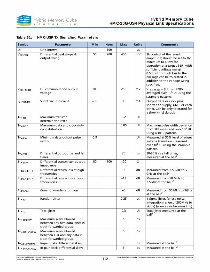
Hybrid Memory CubeHMC-10G-USR Physical Link Specifications
Table 61: HMC-USR TX Signaling Parameters
Symbol Parameter Min Nom Max Units Comments
UI Unit interval 100 ps
VTX-DIFF Differential peak-to-peak output swing
50 200 400 mV 3b control of the launch amplitude; should be set to the minimum to allow for operation at a target BER1 with sufficient voltage margin.0.5dB of through loss to the package can be tolerated in addition to the voltage swing specified.
VTX-CM-DC DC common-mode output voltage
100 250 mV VTX-CM-DC = (TXP + TXN)/2 averaged over 106 UI using the scramble pattern.
ISHORT-TX Short circuit current –30 30 mA Output data or clock pins shorted to supply, GND, or each other. Can be only tolerated for a short (<1s) duration.
TTX-DJ Maximum transmit deterministic jitter
0.2 UI
TTX-DCD Maximum data and clock duty cycle distortion
0.05 UI Maximum pulse width deviation from 1UI measured over 106 UI using a 1010 pattern.
TTX-PW Minimum data output pulse width
0.9 UI Measured at 50% level of edges voltage transition measured over 106 UI using the scramble pattern.
TTX-TRF Differential output rise and fall times
20 ps 20-80% rise fall times, measured at the ball2
ZTX-DIFF Differential transmitter output impedance
80 100 120
RLTX-DIFF-HF Differential return loss at high frequencies
–8 dB Measured from 2.5 GHz to 5 GHz at the ball2
RLTX-DIFF-LF Differential return loss at low frequencies
–12 dB Measured from 50 MHz to 2.5GHz at the ball2
RLTX-CM Common-mode return loss –6 dB Measured from 50 MHz to 5GHz at the ball2
TTX-RJ Random Jitter 0.25 ps 1 sigma jitter. (phase noise integration range of 200MHz to 5GHz) (source synchronous link)
TTX-TJ Total jitter 0.3 UI Total jitter measured at the ball2
TTX-DSKEW Maximum skew allowed between any two data lanes in clock forwarded group
5 ps
TTX-DCLKSKEW Maximum skew allowed between CLK and any data in clock forwarded group
5 ps
TTX-PNDSKEW In-pair data differential skew 3 ps Measured at the ball2
TTX-PNCKSKEW In-pair clock differential skew 3 ps Measured at the ball2
PDF: 09005aef84936aaf/Source: 09005aef84936abb The Hybrid Memory Cube Consortium reserves the right to change specifications without notice.10G-USR_Physical_Link_Specifications.fm - Rev. 1.0 1/13 EN 112
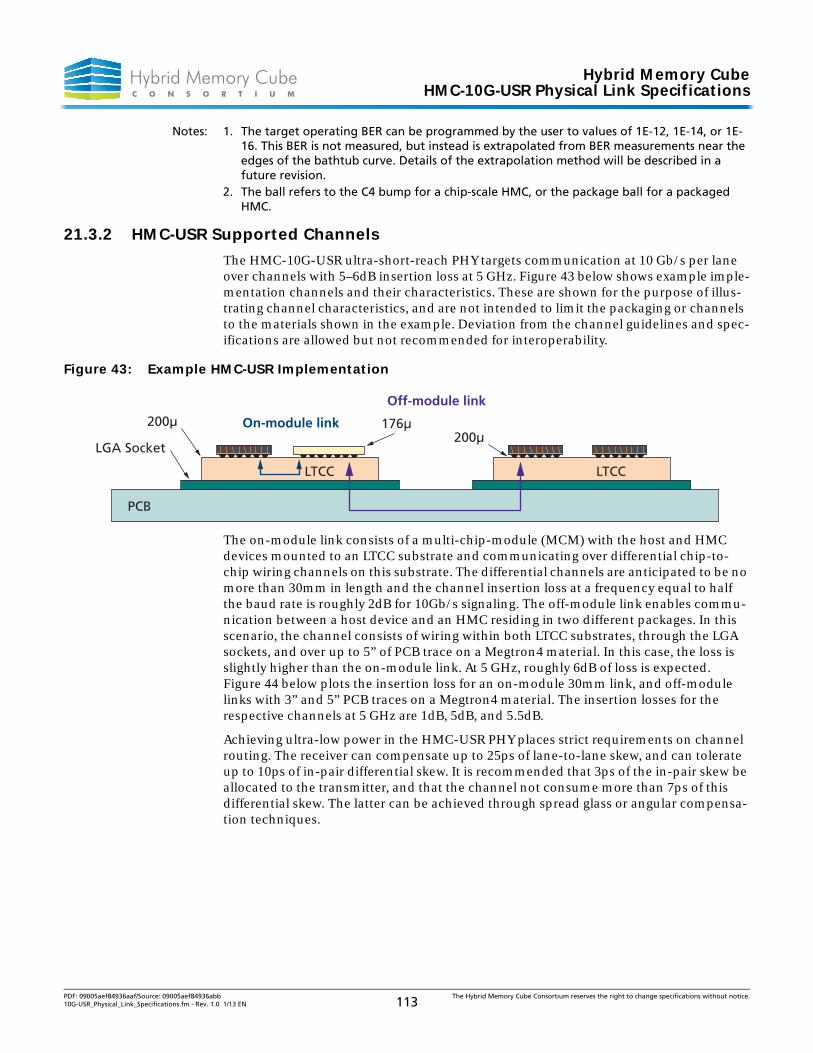
Hybrid Memory CubeHMC-10G-USR Physical Link Specifications
Notes: 1. The target operating BER can be programmed by the user to values of 1E-12, 1E-14, or 1E-16. This BER is not measured, but instead is extrapolated from BER measurements near the edges of the bathtub curve. Details of the extrapolation method will be described in a future revision.
2. The ball refers to the C4 bump for a chip-scale HMC, or the package ball for a packaged HMC.
21.3.2 HMC-USR Supported Channels
The HMC-10G-USR ultra-short-reach PHY targets communication at 10 Gb/s per lane over channels with 5–6dB insertion loss at 5 GHz. Figure 43 below shows example imple-mentation channels and their characteristics. These are shown for the purpose of illus-trating channel characteristics, and are not intended to limit the packaging or channels to the materials shown in the example. Deviation from the channel guidelines and spec-ifications are allowed but not recommended for interoperability.
Figure 43: Example HMC-USR Implementation
The on-module link consists of a multi-chip-module (MCM) with the host and HMC devices mounted to an LTCC substrate and communicating over differential chip-to-chip wiring channels on this substrate. The differential channels are anticipated to be no more than 30mm in length and the channel insertion loss at a frequency equal to half the baud rate is roughly 2dB for 10Gb/s signaling. The off-module link enables commu-nication between a host device and an HMC residing in two different packages. In this scenario, the channel consists of wiring within both LTCC substrates, through the LGA sockets, and over up to 5” of PCB trace on a Megtron4 material. In this case, the loss is slightly higher than the on-module link. At 5 GHz, roughly 6dB of loss is expected. Figure 44 below plots the insertion loss for an on-module 30mm link, and off-module links with 3” and 5” PCB traces on a Megtron4 material. The insertion losses for the respective channels at 5 GHz are 1dB, 5dB, and 5.5dB.
Achieving ultra-low power in the HMC-USR PHY places strict requirements on channel routing. The receiver can compensate up to 25ps of lane-to-lane skew, and can tolerate up to 10ps of in-pair differential skew. It is recommended that 3ps of the in-pair skew be allocated to the transmitter, and that the channel not consume more than 7ps of this differential skew. The latter can be achieved through spread glass or angular compensa-tion techniques.
LGA Socket
200μ On-module link
LTCC
Off-module link
LTCC
PCB
200μ176μ
PDF: 09005aef84936aaf/Source: 09005aef84936abb The Hybrid Memory Cube Consortium reserves the right to change specifications without notice.10G-USR_Physical_Link_Specifications.fm - Rev. 1.0 1/13 EN 113
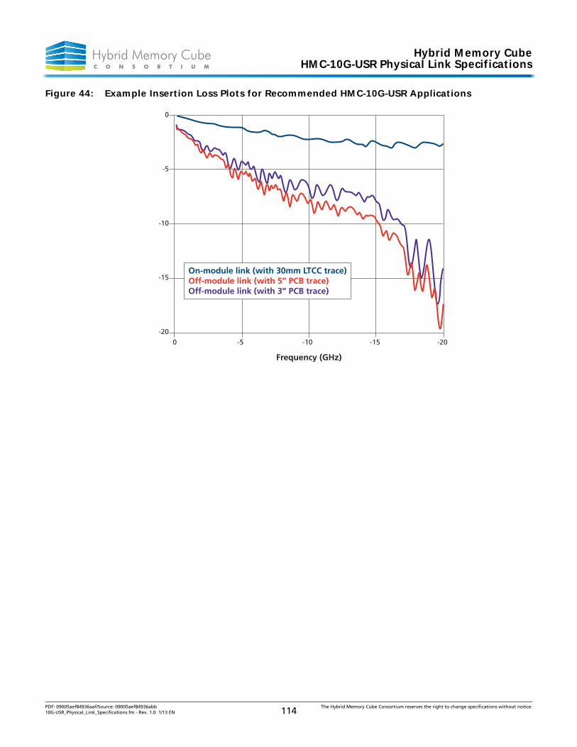
Hybrid Memory CubeHMC-10G-USR Physical Link Specifications
Figure 44: Example Insertion Loss Plots for Recommended HMC-10G-USR Applications
0
-5
-10
-15
-20
0 -5 -10 -15 -20
Frequency (GHz)
On-module link (with 30mm LTCC trace)Off-module link (with 5” PCB trace)Off-module link (with 3” PCB trace)
PDF: 09005aef84936aaf/Source: 09005aef84936abb The Hybrid Memory Cube Consortium reserves the right to change specifications without notice.10G-USR_Physical_Link_Specifications.fm - Rev. 1.0 1/13 EN 114
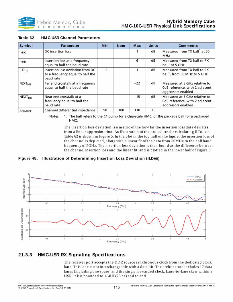
Hybrid Memory CubeHMC-10G-USR Physical Link Specifications
Notes: 1. The ball refers to the C4 bump for a chip-scale HMC, or the package ball for a packaged HMC.
The insertion loss deviation is a metric of the how far the insertion loss data deviates from a linear approximation. An illustration of the procedure for calculating ILDHB in Table 62 is shown in Figure 5. In the plot in the top half of the figure, the insertion loss of the channel is depicted, along with a linear fit of the data from 50MHz to the half baud frequency of 5GHz. The insertion loss deviation is then found as the difference between the channel insertion loss and the linear fit, and is plotted in the lower half of Figure 5.
Figure 45: Illustration of Determining Insertion Loss Deviation (ILDHB)
21.3.3 HMC-USR RX Signaling Specifications
The receiver port accepts the DDR source synchronous clock from the dedicated clock lane. This lane is not interchangeable with a data bit. The architecture includes 17 data lanes (including one spare) and the single forwarded clock. Lane-to-lane skew within a USR link is bounded to 1/4UI (25 ps) end to end.
Table 62: HMC-USR Channel Parameters
Symbol Parameter Min Nom Max Units Comments
ILDC DC insertion loss 1 dB Measured from TX ball1 at 50 MHz
ILHB Insertion loss at a frequency equal to half the baud rate
6 dB Measured from TX ball to RX ball1 at 5 GHz
ILDHB Insertion loss deviation from DC to a frequency equal to half the baud rate
–1 1 dB Measured from TX ball to RX ball1, from 50 MHz to 5 GHz
FEXTHB Far end crosstalk at a frequency equal to half the baud rate
–22 dB Measured at 5 GHz relative to 0dB reference, with 2 adjacent aggressors enabled
NEXTHB Near end crosstalk at a frequency equal to half the baud rate
–15 dB Measured at 5 GHz relative to 0dB reference, with 2 adjacent aggressors enabled
ZCH-DIFF Channel differential impedance 90 100 110
0 0.5 1 1.5 2 2.5 3 3.5 4 4.5 5−1
−0.5
0
0.5
1
Frequency [GHz]
Inse
rtio
n Lo
ss D
evia
tion
(dB)
0 0.5 1 1.5 2 2.5 3 3.5 4 4.5 5−8
−6
−4
−2
0
Inse
rtio
n Lo
ss (d
B)
Frequency [GHz]
5" PCBLinear fit
PDF: 09005aef84936aaf/Source: 09005aef84936abb The Hybrid Memory Cube Consortium reserves the right to change specifications without notice.10G-USR_Physical_Link_Specifications.fm - Rev. 1.0 1/13 EN 115
Hybrid Memory CubeHMC-10G-USR Physical Link Specifications
To maximize the power transfer to the receiver from the transmission line and to bound the amount of energy reflected back to the source, the differential and common-mode return loss is specified by means of a frequency dependent mask from 50MHz to the fundamental of the maximum bit rate. The return loss is measured with the device powered up and biased over the range of VTR/4 to 3VTR/4. Two single port S11 measure-ments are made for each half of the differential input. These results are then combined into the mixed mode differential S-parameter matrix to extract SDD11.
21.3.3.1 Jitter Model
Interoperability is ensured by specifying the total jitter (TJ) of the transmitter and the total jitter of the receiver. TJ can be calculated by the Dual Dirac approximation of the random and deterministic components of jitter, RJ and DJ. The total jitter of the Trans-mitter TTX-EYE is 30 % of the UI (30ps). The total jitter of the receiver TRX-EYE is 40% of the UI (40ps). Jitter measurements for this source synchronous link are made with the clock as the trigger.
Table 63: HMC-USR RX Signaling Parameters
Symbol Parameter Min Nom Max Units Comments
UI Unit interval 100 ps ± is set by the reference clock oscillator
VRX-DIFF-MAX Maximum differential peak-to-peak input swing
400 mV Maximum outer eye, measured over 106 UI with compliant TX and channel. TX sends the scramble pattern.
VRX-DIFF-MIN Minimum differential peak-to-peak input swing
50 mV Minimum inner eye, measured over 106 UI with compliant TX and channel. TX sends the scramble pattern.
VRX-CM-DC DC common-mode output voltage
100 250 mV VTX-CM-DC = (RXP + RXN)/2 averaged over 106 UI with the transmitter sending the scramble pattern.
ISHORT-RX Short circuit current –15 15 mA Input data or clock pins shorted to supply, GND, or each other. Can only be tolerated for short (<1s) duration.
TRX-DJ Maximum deterministic jitter receiver must tolerate
0.5 UI
TRX-CLK-TJ-HF High frequency total jitter on clock
0.05 UI Cycle-to-cycle jitter applied to receiver’s CLK during jitter tolerance testing.
TRX-PW Minimum data input pulse width
0.5 UI Measured at 50% level of edge’s voltage transition.
TRX-CLK-PW Minimum clock input pulse width
95 100 105 ps Measured at 50% level of edge’s voltage transition.
TRX-DSKEW Maximum skew allowed between any two data lanes in clock forwarded group
25 ps The receiver is designed to compensate up to 25ps lane-to-lane static skew, measured at the input ball1.
TRX-DCLKSKEW Maximum skew allowed between CLK and any data in clock forwarded group
25 ps The clock can fall anywhere in the 25ps total data skew, measured at the input ball1.
PDF: 09005aef84936aaf/Source: 09005aef84936abb The Hybrid Memory Cube Consortium reserves the right to change specifications without notice.10G-USR_Physical_Link_Specifications.fm - Rev. 1.0 1/13 EN 116
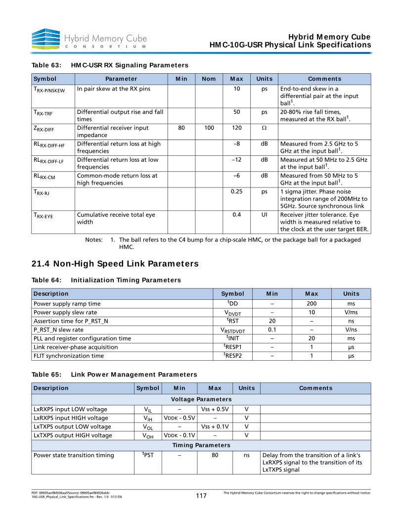
Hybrid Memory CubeHMC-10G-USR Physical Link Specifications
Notes: 1. The ball refers to the C4 bump for a chip-scale HMC, or the package ball for a packaged HMC.
21.4 Non-High Speed Link Parameters
TRX-P/NSKEW In pair skew at the RX pins 10 ps End-to-end skew in a differential pair at the input ball1.
TRX-TRF Differential output rise and fall times
50 ps 20-80% rise fall times, measured at the RX ball1.
ZRX-DIFF Differential receiver input impedance
80 100 120
RLRX-DIFF-HF Differential return loss at high frequencies
–8 dB Measured from 2.5 GHz to 5 GHz at the input ball1.
RLRX-DIFF-LF Differential return loss at low frequencies
–12 dB Measured at 50 MHz to 2.5 GHz at the input ball1.
RLRX-CM Common-mode return loss at high frequencies
–6 dB Measured from 50 MHz to 5 GHz at the input ball1.
TRX-RJ 0.25 ps 1 sigma jitter. Phase noise integration range of 200MHz to 5GHz. Source synchronous link
TRX-EYE Cumulative receive total eye width
0.4 UI Receiver jitter tolerance. Eye width is measured relative to the clock at the user target BER.
Table 64: Initialization Timing Parameters
Description Symbol Min Max Units
Power supply ramp time tDD – 200 ms
Power supply slew rate VDVDT – 10 V/ms
Assertion time for P_RST_N tRST 20 – ns
P_RST_N slew rate VRSTDVDT 0.1 – V/ns
PLL and register configuration time tINIT – 20 ms
Link receiver-phase acquisition tRESP1 – 1 µs
FLIT synchronization time tRESP2 – 1 µs
Table 65: Link Power Management Parameters
Description Symbol Min Max Units Comments
Voltage Parameters
LxRXPS input LOW voltage VIL – Vss + 0.5V V
LxRXPS input HIGH voltage VIH VDDK - 0.5V – V
LxTXPS output LOW voltage VOL – Vss + 0.1V V
LxTXPS output HIGH voltage VOH VDDK - 0.1V – V
Timing Parameters
Power state transition timing tPST – 80 ns Delay from the transition of a link's LxRXPS signal to the transition of its LxTXPS signal
Table 63: HMC-USR RX Signaling Parameters
Symbol Parameter Min Nom Max Units Comments
PDF: 09005aef84936aaf/Source: 09005aef84936abb The Hybrid Memory Cube Consortium reserves the right to change specifications without notice.10G-USR_Physical_Link_Specifications.fm - Rev. 1.0 1/13 EN 117
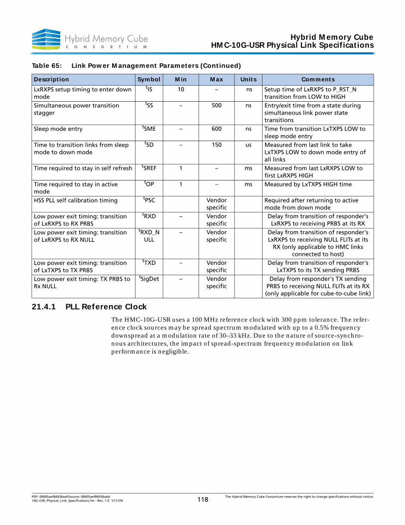
Hybrid Memory CubeHMC-10G-USR Physical Link Specifications
21.4.1 PLL Reference Clock
The HMC-10G-USR uses a 100 MHz reference clock with 300 ppm tolerance. The refer-ence clock sources may be spread spectrum modulated with up to a 0.5% frequency downspread at a modulation rate of 30–33 kHz. Due to the nature of source-synchro-nous architectures, the impact of spread-spectrum frequency modulation on link performance is negligible.
LxRXPS setup timing to enter down mode
tIS 10 – ns Setup time of LxRXPS to P_RST_N transition from LOW to HIGH
Simultaneous power transition stagger
tSS – 500 ns Entry/exit time from a state during simultaneous link power state transitions
Sleep mode entry tSME – 600 ns Time from transition LxTXPS LOW to sleep mode entry
Time to transition links from sleep mode to down mode
tSD – 150 us Measured from last link to take LxTXPS LOW to down mode entry of all links
Time required to stay in self refresh tSREF 1 – ms Measured from last LxRXPS LOW to first LxRXPS HIGH
Time required to stay in active mode
tOP 1 – ms Measured by LxTXPS HIGH time
HSS PLL self calibration timing tPSC Vendor specific
Required after returning to active mode from down mode
Low power exit timing: transition of LxRXPS to RX PRBS
tRXD – Vendor specific
Delay from transition of responder's LxRXPS to receiving PRBS at its RX
Low power exit timing: transition of LxRXPS to RX NULL
tRXD_NULL
– Vendor specific
Delay from transition of responder's LxRXPS to receiving NULL FLITs at its
RX (only applicable to HMC links connected to host)
Low power exit timing: transition of LxTXPS to TX PRBS
tTXD – Vendor specific
Delay from transition of responder's LxTXPS to its TX sending PRBS
Low power exit timing: TX PRBS to Rx NULL
tSigDet – Vendor specific
Delay from responder's TX sending PRBS to receiving NULL FLITs at its RX (only applicable for cube-to-cube link)
Table 65: Link Power Management Parameters (Continued)
Description Symbol Min Max Units Comments
PDF: 09005aef84936aaf/Source: 09005aef84936abb The Hybrid Memory Cube Consortium reserves the right to change specifications without notice.10G-USR_Physical_Link_Specifications.fm - Rev. 1.0 1/13 EN 118
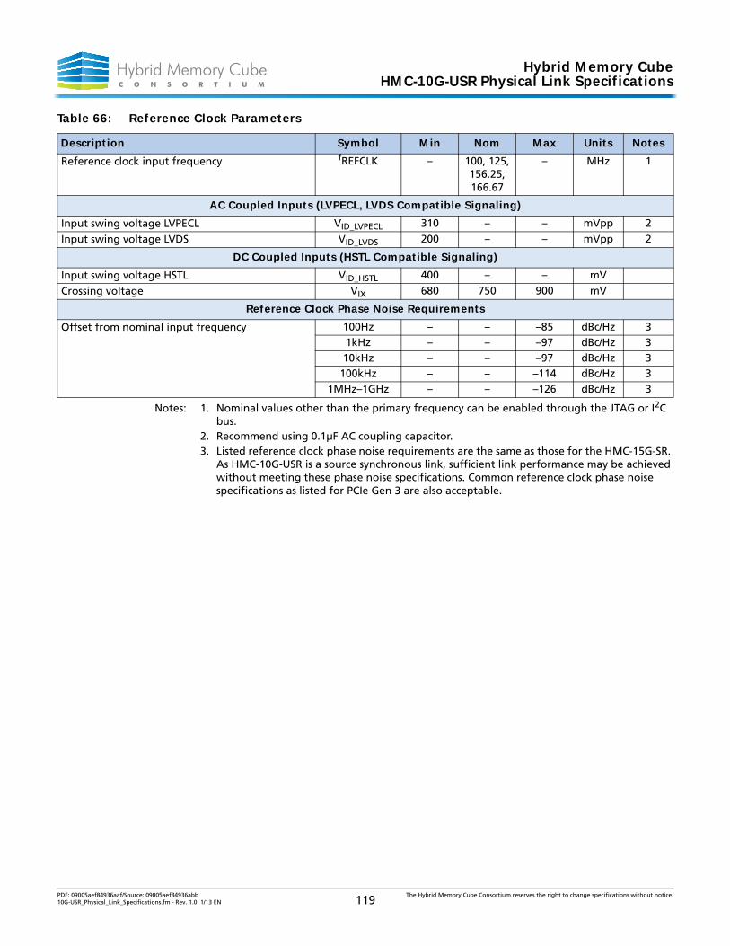
Hybrid Memory CubeHMC-10G-USR Physical Link Specifications
Notes: 1. Nominal values other than the primary frequency can be enabled through the JTAG or I2C bus.
2. Recommend using 0.1µF AC coupling capacitor.3. Listed reference clock phase noise requirements are the same as those for the HMC-15G-SR.
As HMC-10G-USR is a source synchronous link, sufficient link performance may be achieved without meeting these phase noise specifications. Common reference clock phase noise specifications as listed for PCIe Gen 3 are also acceptable.
Table 66: Reference Clock Parameters
Description Symbol Min Nom Max Units Notes
Reference clock input frequency fREFCLK – 100, 125, 156.25, 166.67
– MHz 1
AC Coupled Inputs (LVPECL, LVDS Compatible Signaling)
Input swing voltage LVPECL VID_LVPECL 310 – – mVpp 2
Input swing voltage LVDS VID_LVDS 200 – – mVpp 2
DC Coupled Inputs (HSTL Compatible Signaling)
Input swing voltage HSTL VID_HSTL 400 – – mV
Crossing voltage VIX 680 750 900 mV
Reference Clock Phase Noise Requirements
Offset from nominal input frequency 100Hz – – –85 dBc/Hz 31kHz – – –97 dBc/Hz 310kHz – – –97 dBc/Hz 3
100kHz – – –114 dBc/Hz 31MHz–1GHz – – –126 dBc/Hz 3
PDF: 09005aef84936aaf/Source: 09005aef84936abb The Hybrid Memory Cube Consortium reserves the right to change specifications without notice.10G-USR_Physical_Link_Specifications.fm - Rev. 1.0 1/13 EN 119
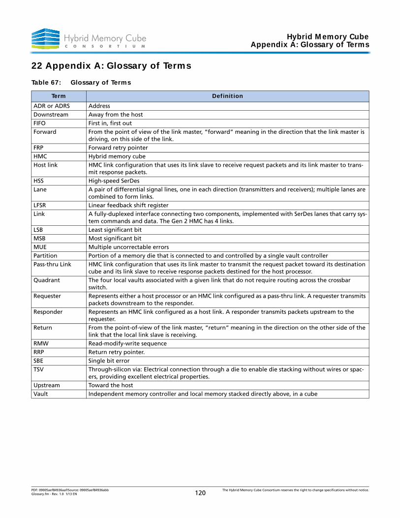
Hybrid Memory CubeAppendix A: Glossary of Terms
22 Appendix A: Glossary of Terms
Table 67: Glossary of Terms
Term Definition
ADR or ADRS AddressDownstream Away from the hostFIFO First in, first outForward From the point of view of the link master, “forward” meaning in the direction that the link master is
driving, on this side of the link.FRP Forward retry pointerHMC Hybrid memory cubeHost link HMC link configuration that uses its link slave to receive request packets and its link master to trans-
mit response packets.HSS High-speed SerDesLane A pair of differential signal lines, one in each direction (transmitters and receivers); multiple lanes are
combined to form links.LFSR Linear feedback shift registerLink A fully-duplexed interface connecting two components, implemented with SerDes lanes that carry sys-
tem commands and data. The Gen 2 HMC has 4 links. LSB Least significant bitMSB Most significant bitMUE Multiple uncorrectable errorsPartition Portion of a memory die that is connected to and controlled by a single vault controllerPass-thru Link HMC link configuration that uses its link master to transmit the request packet toward its destination
cube and its link slave to receive response packets destined for the host processor.Quadrant The four local vaults associated with a given link that do not require routing across the crossbar
switch.Requester Represents either a host processor or an HMC link configured as a pass-thru link. A requester transmits
packets downstream to the responder.Responder Represents an HMC link configured as a host link. A responder transmits packets upstream to the
requester.Return From the point-of-view of the link master, “return” meaning in the direction on the other side of the
link that the local link slave is receiving. RMW Read-modify-write sequenceRRP Return retry pointer.SBE Single bit errorTSV Through-silicon via: Electrical connection through a die to enable die stacking without wires or spac-
ers, providing excellent electrical properties.Upstream Toward the hostVault Independent memory controller and local memory stacked directly above, in a cube
PDF: 09005aef84936aaf/Source: 09005aef84936abb The Hybrid Memory Cube Consortium reserves the right to change specifications without notice.Glossary.fm - Rev. 1.0 1/13 EN 120

Hybrid Memory CubeRevision History
23 Revision HistoryRev. 1.0. . . . . . . . . . . . . . . . . . . . . . . . . . . . . . . . . . . . . . . . . . . . . . . . . . . . . . . . . . . . . . . . . . . . . . . . . . . . . . . . . . . . . . . . . . . .1/2013
• HMCC Specification
PDF: 09005aef84936aaf/Source: 09005aef84936abb The Hybrid Memory Cube Consortium reserves the right to change specifications without notice.Glossary.fm - Rev. 1.0 1/13 EN 121