Embed Size (px)
Citation preview

9Power Electronics in HEVs
9.1 Introduction
Power electronics is one of the enabling technologies propelling the shift from conven-tional gasoline/diesel engine-powered vehicles to electric, hybrid, and fuel cell vehicles.This chapter discusses power electronics used in HEVs and PHEVs. However, the focusof the chapter is on the unique aspects of power electronics in HEVs and PHEVs.
To explain the types of power electronics circuits used in a HEV, we use the configura-tion of a typical series HEV powertrain as shown in Figure 9.1. In this configuration, theinternal combustion engine (ICE) drives a three-phase permanent magnet synchronousgenerator, whose output is a three-phase voltage with variable frequency and variablevoltage. This output needs to be rectified to a direct current (DC) voltage.
The front wheels are driven by an induction motor which needs to be controlled bya voltage source inverter (VSI) or a current source inverter (CSI). An energy storagesystem is connected to the DC bus, between the generator/rectifier output and the inverter.However, there is a bidirectional DC–DC converter that manages the charge/discharge ofthe battery, as well as controlling the DC bus voltage.
In conventional vehicles, the air-conditioning (A/C) compressor is driven by the enginethrough a belt. In advanced HEVs, the engine is turned off very often during stop-and-godriving patterns. In order to have A/C while the engine is off, the A/C compressor needsto be driven by an electric motor which runs from the hybrid battery. There may be anelectrically driven hydraulic pressure pump for the vehicle’s hydraulic systems, such asfrictional brakes, power steering, and so on. The A/C motor and the compressor motorare typically brushless DC motors with an inverter.
In addition, auxiliary components, such as headlights, wipers, entertainment systems,heat seats, and so on, run from the 14 V auxiliary battery. Most advanced hybrid vehiclesno longer have an alternator, which means the 14 V battery needs to be charged fromthe high-voltage (HV) battery. On the other hand, even if an alternator is present, whenthe engine is off, the 14 V battery can still be drained quickly without proper chargemaintenance. Therefore, it is necessary to have a DC–DC converter to charge the 14 Vbattery from the hybrid battery. For PHEV, there is also a battery charger installed on thevehicle or in the charging station.
Hybrid Electric Vehicles: Principles and Applications with Practical Perspectives, First Edition.Chris Mi, M. Abul Masrur and David Wenzhong Gao.© 2011 John Wiley & Sons, Ltd. Published 2011 by John Wiley & Sons, Ltd. ISBN: 978-0-470-74773-5

198 Hybrid Electric Vehicles
HV Battery
Inverter Motor MechanicalTransmission
Wheel
Wheel
GeneratorEngine Rectifier
DC-DCConverter
PressureMotor
Inverter DC-DCConverter
AuxiliaryBattery
Figure 9.1 Power electronics converters used in a series HEV
Even though there are commonalities between the power converters used in HEVsand the ones used in other industrial, commercial, or residential applications, there aresome unique features specific to automotive applications. Examples include wider ambientoperating temperature (−20 to 50 ◦C), vibration and shock, electromagnetic compatibility,and thermal management.
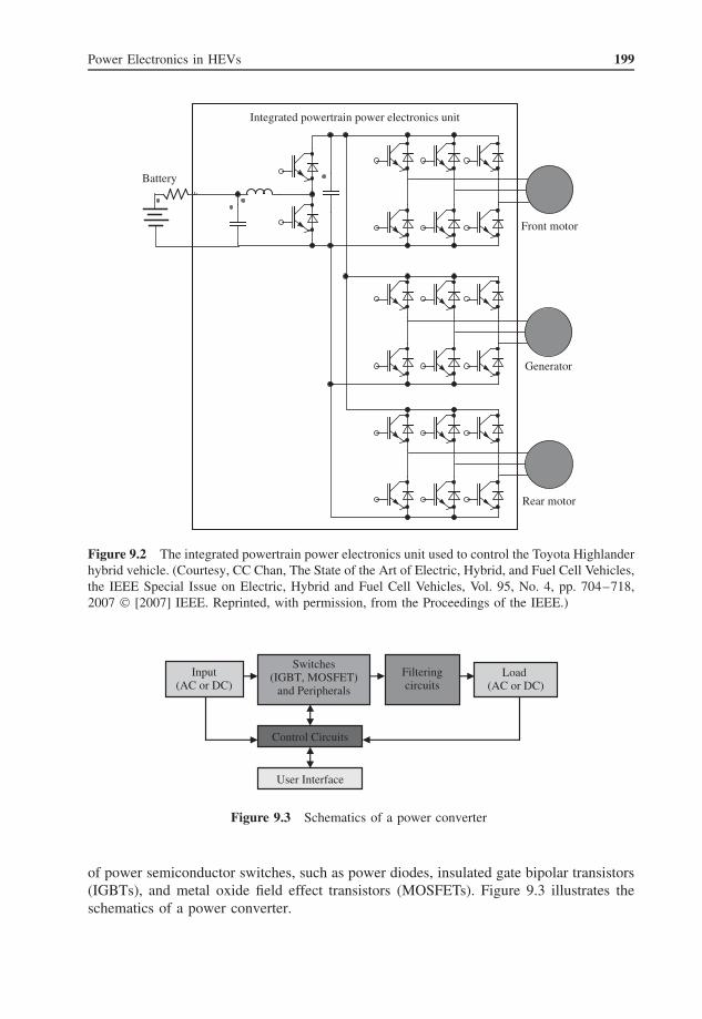
Figure 9.2 shows the integrated main power electronics unit used to control the Toy-ota Highlander HEV (http://www.toyota.com). The power electronics unit consists of abidirectional DC–DC converter that links the hybrid battery and the DC bus, and threemotor drive circuits that control the front and rear motor/generators.
The issues to be addressed in the design of HEV power electronics circuitscover [1–23]:
• Electrical design: Includes main switching circuit design; controller circuitry design;switching frequency optimization; and loss calculations.
• Control algorithm design: Includes developing the control algorithm to achieve thedesired voltage, current, and frequency at the output, and to realize bidirectional powerflow as needed.
• Magnetic design: Includes the design of inductors, transformers, and other componentssuch as capacitors needed for filtering, switching, and the gate driver units.
• EMC design: Includes understanding the electromagnetic interference (EMI) issues,analyzing switching transients, and circuit layout that minimizes parasitic inductanceand capacitances.
• Mechanical and thermal design: Includes modeling of the loss of power devices andmagnetic components; cooling system, heat sink, and enclosure design; and integrationof the power electronics unit.
9.2 Principle of Power Electronics
In broad terms, power electronics is a discipline that studies power converters which pro-cess and control power flow using electronic means. It mainly involves the use and control
Power Electronics in HEVs 199
Integrated powertrain power electronics unit
Front motor
Generator
Rear motor
Battery
Figure 9.2 The integrated powertrain power electronics unit used to control the Toyota Highlanderhybrid vehicle. (Courtesy, CC Chan, The State of the Art of Electric, Hybrid, and Fuel Cell Vehicles,the IEEE Special Issue on Electric, Hybrid and Fuel Cell Vehicles, Vol. 95, No. 4, pp. 704–718,2007 © [2007] IEEE. Reprinted, with permission, from the Proceedings of the IEEE.)
Load (AC or DC)
Switches(IGBT, MOSFET)
and Peripherals
Control Circuits
Input(AC or DC)
User Interface
Filteringcircuits
Figure 9.3 Schematics of a power converter
of power semiconductor switches, such as power diodes, insulated gate bipolar transistors(IGBTs), and metal oxide field effect transistors (MOSFETs). Figure 9.3 illustrates theschematics of a power converter.

200 Hybrid Electric Vehicles
As can be seen from Figure 9.3, a typical power converter will consist of four segments:switching and peripheral circuits, filtering circuits, control circuits and feedback, and anoptional user interface:
• Types of power converters: Power converters are usually classified by their input andoutput. Since the input and output of a power converter can be either alternate current(AC) or direct current (DC), there can be four types of power converters:– DC–DC converter– DC–AC inverter– AC–DC rectifier– AC–AC cycloconverter.The first three types of power converters are all used in HEVs. The fourth type, AC–ACcycloconverters, is only used in high-power AC–AC systems to control the voltagemagnitude and frequency of large motors. However, AC–AC conversion involving anAC–DC circuit and a DC–AC circuit is not unusual. Depending on the powertrain con-figuration and level of hybridization, a HEV can involve one or more power convertersof different types.
• Main circuit (switches, peripherals): The main circuit consists of power semiconduc-tor devices (switches and diodes) and peripheral circuits. The semiconductor switchesare controlled to turn on and turn off at a frequency ranging from a few kilohertz toa few tens of kilohertz for HEV applications. Depending on the voltage level of thesystems, both MOSFETs and IGBTs are used in HEV power converters.
• Filtering circuit: Power electronics converters usually involve LC low-pass filtersthat will filter out the high-frequency components of the output voltage and let thelow-frequency components or DC component pass to the load side.
• Control and feedback circuit: Control and feedback typically involve the use ofmicrocontrollers and sensors. HEV powertrain applications usually involve feedbacktorque control. Current feedback is usually necessary.
As a well-developed discipline, power electronics has been very well covered in manytextbooks. This chapter will only focus on the unique aspects of power electronics per-taining to HEV applications.
9.3 Rectifiers Used in HEVs
Rectifiers are used to convert an AC input to a DC output. Even though controlledrectifiers exist, they are rarely used in automotive applications. Therefore, we will onlydiscuss uncontrolled passive rectifiers and their unique aspects in HEV applications.
9.3.1 Ideal Rectifier
Figure 9.4 shows a single-phase rectifier and a three-phase ideal rectifier operating fromideal voltage sources. With ideal diode characteristics, the output of a single-phase rectifiercan be expressed as
Vo = 1
T /2
∫ T /2
0
√2Vi sin(ωt)dt = 0.9Vi (9.1)

Power Electronics in HEVs 201
Vi
D1
R1
D2
D3
D4
Rin
Vo
(V)
0
350
50
100
150
200
250
300
0 33.4m5m 10m 15m 20m 25mTime (Seconds)
Vo
Va
D1
R1
D2
D3
D4
Vo
(V)
0
600
100
200
300
400
500
0 16.8m2.5m 5m 7.5m 10m 12.5mTime (Seconds)
Vo
D5
D6
Vb
Vc
+−
+−
+− +
−
Figure 9.4 Ideal rectifiers: top, single-phase rectifier circuit and output voltage waveforms;bottom, three-phase rectifier circuit and output voltage waveforms
where V o is the output voltage, V i is the rms value of the input voltage, T is the periodof the input voltage, and ω is the angular frequency of the input.
The output of an ideal three-phase rectifier is
Vo = 1
π/3
∫ π/6
−π/6(Va − Vb)dt = 1
π/3
∫ π/6
−π/6
√2VLL cos(ωt)dt = 1.35VLL (9.2)
where V LL is the rms value of line-to-line voltage.
9.3.2 Practical Rectifier
In HEV applications, the input to a rectifier is usually the output of a synchronous genera-tor (such as in a series HEV or complex HEV), or an alternator (in a belt–alternator–starterHEV). The circuit and output voltage waveforms of a practical HEV rectifier are shown inFigure 9.5. The generator impedance is in series with the voltage source, and the voltagedrop of the diodes is also included. It can be seen that there is a significant amount ofvoltage drop in a practical rectifier when compared to an ideal rectifier. The voltage dropis caused by the impedance of the generator, which is generally not negligible, differentfrom that of rectifiers connected to an infinite AC grid. Besides, there will be commu-tation loss due to the inductance of the generator. Therefore, the output voltage can be

202 Hybrid Electric Vehicles
Va
D1
Ro
D2
D3
D4
Vo
D5
D6
Vb
Vc
C1
RaLa
RbLb
RcLc
Vo
(V)
425
575
450
475
500
525
550
25m 50m30m 35m 40m 45m
Time (Seconds)
+
−+
−+
−
Figure 9.5 Practical rectifiers used in a HEV: top, rectifier circuit; bottom, output voltage incomparison to ideal rectifier (upper curve: ideal rectifier; lower curve: practical rectifier)
significantly different between no-load and loaded conditions. The difference is definedas voltage regulation.
9.3.3 Single-Phase Rectifier
We will use a single-phase circuit to analyze the voltage regulation, voltage ripple,and commutation.
At no-load conditions, due to the existence of the output capacitor, the output voltagewill equal the peak of the input voltage, that is,
Vo =√
2Va = 1.414Va (9.3)
When load current increases, the impedance of the generator, and the diodes, will have avoltage drop on them. If the DC link capacitor is sufficiently large, then we can assume

Power Electronics in HEVs 203
that the output voltage V 1 (DC link voltage) is constant. We further assume that diodevoltage drop V D is also a constant.
By solving√
2Va sin ωt = 2VD + V1, we get
θ1 = ωt0 = arcsin
(2VD + V1√
2Va
)(9.4)
The analysis can be divided into two scenarios: discontinuous and continuous mode. Indiscontinuous mode, the AC side current is not continuous. The current starts from zeroand builds up when ωt ≥ θ1; it reaches a maximum when
√2Vi sin ωt = 2VD + Vo (ωt = π − θ1) (9.5)
The current then drops to zero at θ2, θ2 < π + θ1.Continuous Mode: In continuous mode, the AC side current does not reach 0 at π + θ1.
In other words, θ2 >π + θ1.In continuous mode, the voltage equation is
Vi − La
di
dt− Rai − 2VD = V1, i(t0) = 0 (9.6)
di
dt+ Ra
La
i = 1
La
(√2Va sin ωt − 2VD − V1
)when ωt ≥ θ1 (9.7)
Note that the AC input will not have current until the voltage exceeds the output voltageplus the diode drop. However, the current will continue to flow until it reaches zero atangle θ2.
We further neglect the resistance. The above differential equation can be simplified andthe following solution obtained:
i(t) = −√
2Va
ωLa
cos ωt − 2VD + V1
ωLa
ωt + C, θ1 ≤ ωt ≤ θ2 (9.8)
Since i (θ1) = 0, from the above equation we get
C =√
2Va
ωLa
cos θ1 + 2VD + V1
ωLa
θ1 (9.9)
Therefore,
i(t) = −√
2Va
ωLa
(cos ωt − cos θ1) − 2VD + V1
ωLa
(ωt − θ1), θ1 ≤ ωt ≤ θ2 (9.10)
To find θ2,
1
ωLa
∫ θ2
θ1
(√2Va sin ωt − 2VD − V1
)dωt =0 (9.11)
cos θ2 + 2VD + V1√2Va
θ2 = cos θ1 + 2VD + V1√2Va
θ1 (9.12)

204 Hybrid Electric Vehicles
Va
D1
Ro
D2
D3
D4
C1RaLa+
−
Figure 9.6 Voltage regulation, commutation of practical rectifier used in HEV
The output power of the rectifier must be equal to the power consumed by the load:
P = 1
π
∫ θ2
θ1
√2Va sin ωt∗i(t)d(ωt) = V 2
1
R(9.13)
so the output voltage of the rectifier is
Vo =√
R
π
∫ θ2
θ1
√2Va sin ωt∗i(t)d(ωt) (9.14)
The above expression cannot be directly solved due to the fact that θ1 and θ2 are functionsof V o . But it can be seen that the rectifier output is closely related to the impedance ofthe generator.
The voltage regulation can then be calculated from Figure 9.6. That is,
�Vo = V1 − Vo
Vo
× 100% (9.15)
Apparently, the voltage regulation is a function of the internal impedance of the generator,and the output power.
9.3.4 Voltage Ripple
The above derivation assumes that the output voltage is constant. However, it can be seenthat the current from the AC input is discontinuous. This means that, during the portionof the cycle when there is no current from the AC side (e.g., from 0 to θ1, and from θ2to π if θ2 <π), the load current is supplied by the capacitor.
However, due to the nonlinearity of the current, when the load current is less than theAC side current, the capacitor still has to supply some current to the load. Therefore, wecan assume that if the load current is constant, and also that the capacitor supplies currentto the load 50% of the time, then the voltage ripple is
�Vo = 1
2
1
C
Vo
R
π
ω(9.16)

Power Electronics in HEVs 205
Example: In Figure 9.6, V a = 220 V, 400 Hz, La = 1 mH, Ra = 0.05 (which canbe neglected in the analytical calculations), C = 10 mF, and V D = 0.8 V. The DCoutput is equivalent to 10 �. Find the output voltage and voltage ripple.
Solution: V o can be solved using the above equations and is illustrated inFigure 9.7a. It is then solved in MATLAB (Figure 9.7b).
Vo–Vnew < e ?
Initial Vo
Solve for q1 using
Solve for q1 using
2Va sin w t*i(t)d(wt)R
V1 =
2VD +Vo 2VD + Vo
2Va 2Va
cosq2 q2 = q1cos q1 + +
Solve V1 using
2Va sin w t*i(t)d(wt)R
V1
End
Y
N
Update Vo
p
p
∫
∫
Figure 9.7 (a) Flow chart for solving the circuit shown in Figure 9.6. (b) MATLAB codecorresponding to the flow chart in (a)
The solution is V o = 206 V. The calculated voltage ripple is 1.3 V.Simulation: The same circuit is further simulated in Simplorer. The output volt-
age is 206.3 V, and the voltage ripple is 1 V.
Discontinuous Mode: In discontinuous mode, the AC side current starts atωt = θ1 >θ2, and drops to 0 at ωt >π + θ1:
di
dt+ Ra
La
i = 1
La
(√2Va sin ωt − 2VD − V1
), θ2 ≤ ωt ≤ θ2 + π (9.17)
and
i(π − θ2) = i(θ2) = 0 (9.18)

206 Hybrid Electric Vehicles
% Matlab Program to solve for Vo. clear all syms wt i v y delta_error=0.01; voltage_error=0.1; VD=0.8; Va=220*sqrt(2); w=2*pi*400; La=1e-3; RLoad=10; Ra=0.001; RD=0.001; R=RLoad+2*RD+Ra; x=w*La; %Initialization Vo=Va; V1=0; %Solve for Vo while abs(V1-Vo)>voltage_error Vo=(Vo+V1)/2; c0=(2*VD+Vo)/Va; theta1=asin(c0); c1=cos(theta1)+ c0*theta1; %find theta2 theta2 = pi - theta1; c2 = cos(theta2)+ c0*(theta2); while abs((c2-c1))>delta_error theta2=theta2+0.001; c2 = cos(theta2)+ c0*(theta2); if theta2 >= pi + theta1 break, end end i = -Va/x*(cos(wt)-cos(theta1)) - (2*VD+Vo)/x*(wt-theta1); v = Va*sin(wt); y = simple(i*v); P1 = 1/pi*int(y, wt, theta1, theta2); P = abs(real(eval(P1))); V1 = real(sqrt(P*R)) if V1>=Va V1=Va; end end Io=P/Vo; Vo = Vo - (RD*2*Io + 2*VD) DeltaV=1/C*Vo/RLoad*(theta1+pi-theta2)/w
Figure 9.7 (continued )
When neglecting Ra ,
i(t) = −√
2Va
ωLa
(cos ωt − cos θ2) − 2VD + V1
ωLa
(ωt − θ2), θ2 ≤ ωt ≤ π + θ2 (9.19)
To find θ2, let
1
ωLa
∫ π+θ2
θ2
(√2Va sin ωt − 2VD − V1
)dωt = 0 (9.20)

Power Electronics in HEVs 207
θ2 = arccos
[π(2VD + V1)
2√
2Va
](9.21)
The boundary condition is θ1 = θ2. Therefore, the boundary condition occurs when
2VD + V1 = 2√
2Va√π2 + 4
(9.22)
The above analysis is based on a single-phase generator. Since most generators and motorsare three phase, it is worth looking at three-phase circuits.
Again, if the output capacitor is sufficiently large, then we can assume that the outputvoltage is constant. The diodes only conduct 60◦ in each cycle. The voltage equation canbe written as
VLL − 2La
di
dt− 2Rai − 2VD = V1, −π
6≤ ωt ≤ π
6(9.23)
where V LL is the line–line voltage, and V 1 is the DC link voltage with load. This equationcan be solved using the same method as for the single-phase analysis.
If the generator is a three-phase salient-pole permanent magnet (PM) generator (such asan interior-type PM generator), then the circuit is even more complicated due to the fact thatthe generator has two equivalent inductances, direct-axis and quadrature-axis inductance.
9.4 Buck Converter Used in HEVs
9.4.1 Operating Principle
A buck converter will step down a higher voltage DC input to a lower voltage DC output.The typical application of a buck converter in a HEV is to step down the hybrid batteryvoltage (typically 200–400 V) to charge the auxiliary battery (14 V). The uniqueness isthe large difference between the input and output voltage of the converter and the smallduty ratio (3.5%) needed to control the switching. Figure 9.8 shows the main circuit of abuck converter. It consists of a switch, a freewheeling diode, and an LC filter.
The small duty ratio will make control and regulation very difficult. It also affects thedesign of the inductor, capacitor, current ripple, and voltage ripple. As a starting pointfor the analysis, we assume the components are ideal, that is, the voltage drop is zerowhen turned on. We further assume that the output voltage is constant. When the switchis turned on, the voltage across the inductor is
VL = Vd − Vo (9.24)
When the switch is turned off, we assume the circuit is operating in continuous mode;then the voltage drop across the inductor is
VL = −Vo (9.25)
In steady state operations, the average voltage of the inductor must be zero. Therefore,
(Vd − Vo)DTs = Vo(1 − D)Ts (9.26)

208 Hybrid Electric Vehicles
Vin
T1
D1
L1
C1 R1 Vout
+−
Figure 9.8 A buck converter
and
Vo = DVd (9.27)
The current ripple in the inductor is
�IL = 1
LVo(1 − D)Ts (9.28)
The voltage ripple of the output can be calculated. We assume the load current is constant;then all the current ripple will enter the capacitor,
�Vo = 1
C
1
2
�IL
2
Ts
2= T 2
s
8LCVo(1 − D) (9.29)
9.4.2 Nonlinear Model
The above analysis is based on assumptions that the output voltage is relatively constantand the parasitic parameters (resistance, inductance) can be neglected. Due to the factthat the ratio between the input and output voltages is very large, these assumptions maynot hold true.
In order to accurately analyze the relationship and the influence of various parameters,we can use a detailed model to describe the system. In continuous mode, when the switchis turned on,
Vd = rdiL + rsiL + LdiLdt
+ rLiL + Vo (9.30)
iL = ic + io = CdVo
dt+ io = C
dVo
dt+ Vo
R(9.31)
where rd , rs , and rL are the equivalent resistance of the diode, switch, and inductor,respectively; and i o , i c , and i L are the current through the load resistance, the capacitor,and the inductor, respectively.

Power Electronics in HEVs 209
The above equations can be rewritten as⎡⎢⎣
diLdt
dVo
dt
⎤⎥⎦ =
⎡⎢⎣ − rd + rs + rL
L− 1
L1
C− 1
CR
⎤⎥⎦
[iL
Vo
]+
⎡⎣ 1
L0
⎤⎦Vd (9.32)
When the switch is closed,⎡⎢⎣
diLdt
dVo
dt
⎤⎥⎦ =
⎡⎢⎣ − rD + rL
L− 1
L1
C− 1
CR
⎤⎥⎦
[iL
Vo
](9.33)
These equations can be solved using numeric tools such as MATLAB.
9.5 Non-isolated Bidirectional DC–DC Converter
The bidirectional DC–DC converter in a HEV is also sometimes called an energy man-agement converter, or boost DC–DC converter. This DC–DC converter is a high-powerconverter that links the HV battery at a lower voltage with the HV DC bus. The typicalvoltage of a battery pack is designed at 300–400 V. The best operating voltage for amotor and inverter is around 600 V. Therefore, this converter can be used to match thevoltages of the battery system and the motor system. Other functions of this DC–DCconverter include optimizing the operation of the powertrain system, reducing ripple cur-rent in the battery, and maintaining DC link voltage, hence the high-power operation ofthe powertrain.
9.5.1 Operating Principle∗
The DC–DC converter provides bidirectional power transfer. The operating principle isshow in Figure 9.9.
• Buck operation: In buck operation as shown in Figure 9.9b, the power is transferredfrom V d to V B . When T1 is closed and T2 is open, since V d > V B , V L = V d – V B andthe inductor current I L builds up. When T1 is open, the inductor current I L continuesto flow through D2. Thus, V L = V B .Assuming ideal components and a constant V o , the inductor current over one cycle insteady state operation will remain the same, for example,∫ t1on
0(Vd − Vo)dt =
∫ t1on+t1off
t1on
(−Vo)dt (9.34)
Vo = t1on
TVd = D1Vd (9.35)
∗ © [2007] Inderscience. Reprinted, with permission, from the International Journal of Electric and Hybrid Vehicles.

210 Hybrid Electric Vehicles
L1Vd
VB
T1
T2
D1
D2
R
(a)
IL IL
D2
T1
(b)
(c)
ILIL D1T2
VL, ILVL = Vd−Vo
t2on
ILVL = −Vo
VL = −Vo
VL, IL
VL = Vd−Vo
IL
+
−
+
−
+
−
+
−
+
−
+
−
+
−
Figure 9.9 Operation of the bidirectional boost converter: (a) circuit topology; (b) inductor voltageand current waveform during buck operation; and (c) inductor voltage and current waveform duringboost operation

Power Electronics in HEVs 211
where D1 is the duty ratio defined as the percentage of on-time of switch T1:
D1 = t1on
T(9.36)
• Boost operation: In boost operation, the power is transferred from V B to V d . WhenT2 is closed and T1 is open, V B and the inductor form a short circuit through switchT2, as shown in Figure 9.9c, therefore V L = V B and the inductor current I L builds up.When T1 is open, the inductor current continues to flow through D1 to V d , thereforeV L = V d – V B : ∫ t2on
0Vo dt =
∫ t2on+t2off
t2on
(Vd − Vo)dt (9.37)
Vd = 1
1 − D2Vo (9.38)
where D2 is the duty ratio defined as the percentage of on-time of switch T2:
D2 = t2on
T(9.39)
In the bidirectional boost converter control, since T1 and T2 cannot be switched onsimultaneously, a practical control strategy is to turn T2 off while T1 is on and viceversa. In this case,
D2 = 1 − D1 (9.40)
9.5.2 Maintaining Constant Torque Range and Power Capability
The above analysis neglected the internal impedance of the battery. In fact, the impedanceis often not negligible. When an electric motor and inverter are directly connected tothe battery without a bidirectional DC–DC converter as shown in Figure 9.10, as thecurrent (power or torque) goes up, the battery terminal voltage starts to drop because ofthe voltage drop on the battery internal impedance. For example, a 16 kWh lithium-ionbattery with iron phosphate chemistry will have an internal impedance of 0.5 �. If thepowertrain inverter/motor is rated at 125 kW, 400 V, 90% efficiency, the rated currentis 348 A at 400 V. The battery internal voltage drop is 174 V. This voltage drop willsignificantly affect the performance of the powertrain motors. In fact, in this example,the maximum power that can be delivered to the motor is only 78 kW. In addition, dueto the available voltage at the input, the motor constant torque region is also affected. Inthe above example, the constant torque region is shortened by 43.5%.
Another factor is that battery voltage is related to battery state of charge (SOC). Asthe battery SOC drops, the battery voltage will also drop. Therefore, the available voltageat a motor/inverter terminal is also changed, which will make it difficult to maintain theconstant torque range.
When a DC–DC converter is inserted between the battery and inverter/motor as shownin Figure 9.11, the DC bus voltage before the inverter can be maintained as a constant.

212 Hybrid Electric Vehicles
DC/AC M400VC
348A
400V16kWh
+ 174V −
LoadOnly 78kW
Battery Internal Loss48kW
Battery InternalResistance0.5 ohm
Motor Rating125kW, 400V
+−
Figure 9.10 Powertrain motor directly connected to battery without the DC–DC converter: top,circuit topology; bottom, equivalent circuit of the circuit
DC/AC M400V
Vdc = 650V
Figure 9.11 Powertrain motor connected to battery through a DC–DC converter
Therefore, the constant torque range will not be affected by the battery SOC or largepower drawn by the inverter/motor.
The above analysis assumes that the battery system is designed to handle the largepower dissipation during large power draw.
9.5.3 Reducing Current Ripple in the Battery
Due to the switching functions of the inverter used in the powertrain system, there areabundant high-frequency current harmonics on the DC side. The amount of current rip-ple that goes into/out of the battery depends on the switching methodology, switchingfrequency, and the capacitance on the DC bus. When there is no DC–DC converter inplace, the amount of ripple current of the battery is determined by the DC bus capacitanceC and the ratio of capacitor impedance to battery impedance. Without the capacitance,the battery current will be directly determined by the switching status of the DC–AC
Power Electronics in HEVs 213
inverter, that is, the combination of the three-phase current of the motor, as shown inFigure 9.12. When there is a DC bus capacitor in parallel with the battery, the amountof current ripple flowing into/out of the battery is determined by the capacitance andparasitic impedance of the DC bus capacitor. For example, if C = 10 mF, the capacitiveimpedance of the capacitor at switching frequency is only 2.65 m�, which is far less thanthe internal impedance of the battery. Ideally the high-frequency ripple will flow throughthe capacitor and the battery current is supposed to be constant.
However, the parasitic resistance of the capacitor is also not negligible. A high-quality10 mF capacitor has 26 m� internal resistance and the second-class capacitor has 100 m�.The quality of the capacitor affects the current ripple of the battery. The lower the capacitorimpedance, the lower the battery ripples, as shown in Figure 9.12. High-frequency ripplecurrent is believed to be harmful to battery life.
When a DC–DC converter is added, the battery current can be maintained with arelatively small ripple, as shown in Figure 9.13.
9.5.4 Regenerative Braking
The regenerative braking of the two topologies, that is, one with and without a DC–DCconverter, will also be different. In the topology where there is no DC–DC converter, theDC bus voltage will fluctuate during transition from motoring to braking. For example,if the motor is initially motoring at 50 kW, and the battery internal voltage is 400 V with0.5 � internal resistance, then the battery current is 155 A and the DC bus voltage is322 V. If the motor is switched to braking at 50 kW, then the battery current is 110 A andthe DC bus voltage is 455 V. This dramatic change of DC bus voltage will make motorcontrol, such as vector control, very difficult.
On the other hand, in a system that contains a DC–DC converter between theinverter/motor DC bus and the battery, the DC bus voltage can be maintained relativelyconstant. Hence, the transition between motoring and braking is easier to handle.
9.6 Voltage Source Inverter∗
Voltage source inverters (VSIs) are used in hybrid vehicles to control the electric motorsand generators. Figure 9.14 shows the power electronic circuit arrangement of a VSIto control the induction motor, PM synchronous motors, and PM brushless motors. Theswitches are usually IGBTs for high voltage, high-power hybrid configurations or MOS-FETs for low voltage designs.
The output of the VSI is controlled through the means of pulse width-modulated (PWM)signals to produce sinusoidal waveforms. Certain harmonics exists in such a switchingscheme. High switching frequency is used to move away the harmonics from the funda-mental frequency.
9.7 Current Source Inverter∗
Figure 9.15 shows the circuit topology of a current source inverter (CSI). The CSI operatesusing the same principle as in a VSI, with the input as a current source. Three smallcommutating/filtering capacitors may be needed on the AC side.
∗ © [2007] Inderscience. Reprinted, with permission, from the International Journal of Electric and Hybrid Vehicles.

214 Hybrid Electric Vehicles
(a)
300
0.0170.01650.0160.0145 0.015 0.0155
Cur
rent
/A
Time/s
250
200
150
100
50
0
(b)
120
0.01850.0180.01750.0170.01650.016
Time/s
Cur
rent
/A
100
80
60
40
20
0
Figure 9.12 Battery current without a DC–DC converter: (a). DC bus current for no DC-buscapacitance; (b). DC bus current for C = 1 mF, Rc = 100 m� (c) DC bus current for C = 10 mF,Rc = 100 m�

Power Electronics in HEVs 215
(c)
130
120
110
100
90
80
70
60
0.037 0.0375 0.038 0.0385 0.039 0.0395 0.04Time/s
Cur
rent
/A
Figure 9.12 (continued )
0.078 0.08 0.082 0.084 0.086 0.088 0.09 0.092
70
80
90
100
110
120
130
140
Time/s
Cur
rent
/A
Figure 9.13 Battery current when a DC–DC converter is inserted between the inverter and thebattery

216 Hybrid Electric Vehicles
MS3 ~B
A
C
1.00
−1.000 10.00m 17.00m
0
1.00
−1.000 10.00m 17.00m
0
+
−
(a)
(b)
(c)
Figure 9.14 Voltage source inverter: (a) circuit diagram; (b) control of the switches; (c) gatecontrol signal via PWM waveform

Power Electronics in HEVs 217
MS3 ~B
A
C
Figure 9.15 Current source inverter
TWT
+
−+
−
Primary Secondary
Figure 9.16 Isolated bidirectional DC–DC converter
9.8 Isolated Bidirectional DC–DC Converter∗
In some applications, galvanic isolation between the battery and the load units isnecessary and desirable [24]. Figure 9.16 shows a full bridge isolated bidirectionalDC–DC converter.
In Figure 9.16, the primary bridge inverter switches at 20–50 kHz, with 50% dutyratio. The output of the primary is a square wave voltage which is applied to the primarywinding of the isolation transformer. The secondary winding of the transformer thereforewill have a square wave voltage. Without any control at the gating of the secondarybridge converter, the voltage of the secondary of the transformer is rectified through thefour freewheeling diodes. The output voltage will fluctuate with load conditions and theprimary voltage.
∗ © [2008] IET. Reprinted, with permission, from IET Power Electronics.

218 Hybrid Electric Vehicles
9.8.1 Basic Principle and Steady State Operations
Steady state operations of isolated bidirectional DC–DC converters have been studied indetail elsewhere [1, 3, 6]. In this section, we complement these studies by distinguish-ing the operating modes of isolated bidirectional DC–DC converters according to thephase shift angle, load conditions, and output voltage. In this analysis, the dead-band andswitching dynamics will be neglected but will be analyzed later.
In the following analysis, the turns ratio of the transformer is n , the transformer primaryvoltage is V 1, and the switching frequency is f s . For the convenience of analysis, wedefine T s as one half of the switching period, for example, T s = 1/(2f s ). The duty cycleor phase shift is based on a half period, D = t on /T s . Therefore, DT s is the phase shiftbetween the two bridges. Further, ILs is the current of the leakage inductance of thesecondary winding. The output voltage of the secondary bridge is V 2.
9.8.1.1 Heavy Load Conditions
There are a number of different operating modes based on the output current with aboundary condition as illustrated in Figure 9.17. Under heavy load conditions, the inductorcurrent increases from an initial negative value i (t0) < 0 at the beginning of the switchingcycle, and reaches a positive value –i (t0) at the end of the half switching cycle. Sixdifferent segments emerge in each switching cycle as shown in Figure 9.17a. In thefollowing analysis, V 2 is assumed to be large than nV 1.
• Segment 0, [t0, t1]: In this segment, Q1 and Q4 of the primary bridge are turned on.Therefore V 1 and nV 1 are positive. Q6 and Q7 of the secondary bridge are turned on.
t
t
t
t
t6t5t4t3t2t1t0
Ts
nV1
V2
VL
iLS
DTs(1–D) Ts
t
t
t
t
t4t3t2t1t0
Ts
nV1
V2
VL
iLS
DTs(1–D) Ts
t
t
t
t
t6t3 t4 t5t2t1t0
Ts
nV1
V2
VL
iLS
DTs(1–D) Ts
(a) (b) (c)
Figure 9.17 Typical voltage and current waveforms for V 2 > nV 1: (a) waveforms for i(t0) < 0;(b) waveforms for Boundary conditions i(t0) = 0; (c) waveforms for i(t0) > 0

Power Electronics in HEVs 219
Due to the negative current in the inductor, D6 and D7 freewheel, and Q6 and Q7 donot conduct current. Thus, VLs = nV1 + V2V . The inductor current increases linearlyfrom a negative value. At t1, the inductor current reaches 0.
• Segment 1, [t1, t2]: Switches Q1 and Q4 of the primary bridge, and Q6 and Q7 of thesecond bridge, are still turned on; VLs = nV1 + V2. The current continues to increaseexcept that it becomes positive, for example, Q6 and Q7 conduct the current. The totalcurrent increment during interval [t0, t2] (Segments 0 and 1) is
�ILs = DTs
Ls
(V2 + nV1) (9.41)
Hence
i(t2) = i(t0) + DTs
Ls
(nV1 + V2) = Imax (9.42)
• Segment 2, [t2, t3]: In this segment, switches Q1 and Q4 of the primary bridge con-tinue to be turned on, but switches Q6 and Q7 are turned off, and switches Q5
and Q8 are turned on. Diodes D5 and D8 freewheel because the current is positive;VLs = nV1 − V2 < 0.The leakage inductor current increment during interval [t2, t3] is
�ILs = (1 − D)Ts
Ls
(nV1 − V2) (9.43)
Hence
i(t3) = i(t2) + (1 − D)Ts
Ls
(nV1 − V2) (9.44)
A similar analysis could be done for the following three segments due to the symmetryof operation.
• Segment 3, [t3, t4]: Switches Q2 and Q3 of the primary bridge continue to be turnedon, and switches Q5 and Q8 are turned on. The primary voltage of the transformer,hence the secondary voltage, is reversed and the current decreases from i (t3) to zero.D5 and D8 freewheel.
• Segment 4, [t4, t5]. Switches Q2 and Q3 of the primary bridge are turned on, andswitches Q5 and Q8 are turned on. The current decreases linearly to the negativemaximum. Switches Q5 and Q8 conduct current. Hence the current increment in Ls inSegments 3 and 4 is
�ILs = −DTs
Ls
(nV1 + V2) (9.45)
• Segment 5, [t5, t6]: Switches Q5 and Q8 are turned off, and D6 and D7 begin tofreewheel. The current increment in Ls is
�ILs = (1 − D)Ts
Ls
(V2 − nV1) (9.46)

220 Hybrid Electric Vehicles
From the symmetry of the inductance current, i(t0) = −i(t3). From Equations9.41−9.46, the initial inductor current can be obtained
i(t0) = 1
4fsLs
[(1 − 2D)V2 − nV1] (9.47)
The maximum current is
Imax = i(t2) = 1
4fsLs
[−(1 − 2D)nV1 + V2] (9.48)
The above analysis of operating modes is based on the assumption that i(t0) < 0, that is,(1 − 2D)V2 < nV1. If (1 − 2D)V2 = nV1, or
V2 = 1
1 − 2DnV1 (9.49)
then i(t0) = 0. This corresponds to the boundary condition as shown in Figure 9.17bwhich is very similar to the non-isolated boost converter in the steady state operation.Under this circumstance the inductor current increases from zero at the beginning of theswitching cycle and drops to zero at T s .
From Equation 9.49, it seems that V 2 will approach infinity when D reaches 0.5. Butit can be seen from Equation 9.47 that when D = 0.5, i(t0) = −nV1/4fsLs , that is, i (t0)will never reach zero for D = 0.5. Therefore, the boundary can only be met when D isnot equal to 0.5.
9.8.1.2 Light Load Condition
It can be seen from Equation 9.47 that when (1 − 2D)V2 > nV1, then i(t0) > 0. Thiscorresponds to light load conditions. The current and voltage waveforms are shown inFigure 9.17c, where the current increases from a positive value at the beginning of thecycle and drops to a negative value at the end of the half switching cycle.
9.8.1.3 Output Voltage
Equations 9.47–9.49 do not give the expression for the output voltage, except for theboundary condition. In order to derive the expression for the output voltage, let us startwith the average current in the inductor. The average current of the leakage inductancein the half switching cycle can be derived from Figure 9.17a (note that i (t0) < 0),
I = 1
2Ts
[(Imax + i(t0))DTs + (Imax − i(t0))(1 − D)Ts] = 1
2fsLs
D(1 − D)V2 (9.50)
The supplied power is
P1 = nV1I = nV1V2
2fsLs
D(1 − D) (9.51)
Assuming that the load has a fixed resistance, then the output power is
Po = V 22
RL
(9.52)

Power Electronics in HEVs 221
Neglecting the transformer and the switch losses, P1 = Po , then
V2 = nV1
2fsLs
RLD(1 − D) (9.53)
and
I2 = nV1
2fsLs
D(1 − D) (9.54)
Equation 9.53 shows that, for a given switching frequency, leakage inductance, and inputvoltage, the output voltage is proportional to the load resistance and is a function of theduty ratio (phase shift angle). For a given load resistance, the output voltage varies withduty ratio, and reaches a maximum when D = 0.5. For a given duty ratio, the outputvoltage is directly proportional to the load resistance. Therefore, for a given phase shiftangle, under heavy load conditions, or
RL <2fsLs
D(1 − D)(9.55)
V 2 will be less than nV 1.When V 2 drops to less than nV 1, the initial inductor current is confined to a negative
value and the current waveforms are also different from the operations under the conditionof V 2 > nV 1, as shown in Figure 9.18. The boundary condition occurs when S 1 = S 2 =S 3 = S 4 in Figure 9.18b, or (nV1 + V2)DTs = (nV1 − V2)(1 − D)Ts . Therefore, at theboundary condition,
V2 = nV1(1 − 2D) (9.56)
An extreme mode emerges when nV 1 = V 2 as shown in Figure 9.18c, where the inductorcurrent will remain constant during the time interval [DTs, Ts].
t
t
t
t
t4t3t2t1t0
nV1
V2
TsVLs
VLs
ILs
(1–D) Ts t
t
t
tt
t
t
t
t4 t4t3 t3t2 t2t1 t1t0 t0
nV1 nV1
V2V2
Ts TsVLs
ILsILs
(1–D) Ts (1–D) Ts
(a) (b) (c)
Figure 9.18 Typical voltage and current waveforms for V 2 < nV 1 and V 2 = nV 1: (a) Commonmode; (b) Boundary mode; (c) Extreme mode, nV 1 = V2

222 Hybrid Electric Vehicles
It can also been seen from Equation 9.54 that the output current is proportional to theduty ratio (phase shift angle). This may be used to analyze conditions where the outputvoltage needs to be maintained as constant, and the current can be controlled through thephase shift angle.
9.8.1.4 Output Power
Substituting Equation 9.53 into Equation 9.51, the output power Po can be obtained as
Po =(
nV1
2fsLs
)2
D2(1 − D)2RL (9.57)
From Equations 9.51 and 9.57, the output power always has maximum values when andonly when D = 1/2, whether for a fixed resistance RL or a constant output voltage V 2.
When the system is in the voltage closed-loop control mode, that is, V 2 = constant,then decreasing RL will result in the output power increasing since the output power isinversely proportional to RL as shown in Equation 9.52. To maintain V 2 as a constant, itcan be seen from Equation 9.53 that D has to be adjusted accordingly: D(1 − D) ∝ 1/RL
for a given V 1. For fixed V 1 and V 2, the output power reaches a maximum at D = 0.5as shown in 9.51. At this condition, RL = RC = 8fsLsV2/(nV1).
Further decrease of RL < RC will result in the output voltage of the system collapsingand entering the open loop at D = 0.5, that is, V 2 cannot be maintained as a constant.Output voltage V 2 and output power Po will decrease, and are both proportional to RL
as shown in Equations 9.53 and 9.57.Consider Equations 9.47 and 9.57. When D ∈ (0, 1/2], if V 1, V 2 are kept constant
(closed-loop control), with the increase of D the power will increase accompanying thedecrease of the initial current i (t0). Hence the absolute value and the sign of i (t0) representthe load condition. The lower the inductor current i (t0), the higher the output power.
Under open-loop control, that is, for a given D , with the increase of load resistance,V 2 and Po will increase according to Equations 9.53 and 9.57. At the same time, theinitial current increases according to Equation 9.47 due to the increase of V 2. Hence therelations between the initial current and output power are very different in the open-loopand closed-loop operations of the converter.
In order to validate the theoretical analysis, a simulation model was set up withV 1 = 200 V, n = 2, and Ls = 120 μH. In Figure 9.19a,b, with the increase of power, theinitial current decreases from a positive value to a negative value. In Figure 9.19c,d, thevariation of initial current is the opposite. This analysis is in good agreement with theearlier analysis.
The maximum output power is also a function of Ls and f s . Increasing the leakageinductance Ls will decrease the current impact to IGBTs but will reduce the capabilityof the maximum output power of the converter as shown in Equation 9.57. This will bediscussed later in this section.
9.8.2 Voltage Ripple
The above switching modes are inherently nonlinear, which will cause voltage ripple onthe output capacitor. The capacitor current is a combination of the inductor current I L andthe load current I o at different operating modes. From Figure 9.17, the capacitor current

Power Electronics in HEVs 223
60
40
20
0
−40
−20
−60
Pri
mar
y C
urre
nt/A
4.9 4.91 4.92 4.93 4.94 4.95 4.96 4.97 4.98
Time/s × 10−3
30
20
10
0
−20
−10
−30
Pri
mar
y C
urre
nt/A
0.0167 0.0168 0.0168 0.0169 0.0169 0.017Time/s
(a)
(b)
Figure 9.19 Simulated primary current at different voltage and power output: (a) primary currentfor V2 = 500 V, R = 200 �, P = 1.8 kW; (b) primary current for V2 = 600 V, R = 40 �, P =9 kW (c) primary current for D = 1/8, R = 60 �, P = 9.2 kW; (d) primary current for D = 1/8,R = 100 �, P = 13.6 kW
can be written as
iC = −(Io + iL), 0 ≤ t ≤ DTs
iC = iL − Io, DTs ≤ t ≤ Ts (9.58)
The capacitor current is shown in Figure 9.20, where at t = t1 + �2, ILs = Io, orI C (t1 + �2) = 0, that is,
Imax + nV1 − V2
Ls
�2 = Io (9.59)

224 Hybrid Electric Vehicles
10
8
6
4
0
2
−2
−4
−6
−8
−10
Pri
mar
y C
urre
nt/A
8.35 8.4 8.45 8.5 8.55
Time/s × 10−3
150
100
50
0
−100
−50
−150
Pri
mar
y C
urre
nt/A
0.0163 0.0163 0.0163 0.0164 0.0164 0.0164
Time/s
(c)
(d)
Figure 9.19 (continued )
Therefore
�2 = Imax − Io
V2 − nV1Ls (9.60)
Based on energy conservation, P1 = Po, or nV1I = V2Io. Substituting Equation 9.51 forPo , the output current can be obtained:
Io = nV1
2fsLs
D(1 − D) (9.61)

Power Electronics in HEVs 225
t
t3 t4 t6t1t0
ILIo
iLs
iC
DTs (1–D) Ts
Ts
Δ2
t
t3t2 t4 t5 t6t1t0
iLs
iC
DTs(1–D) T
Ts
Δ2
(a) (b)
Figure 9.20 The current ripple in the capacitor: (a) current ripple for i(t0) < 0; (b) current ripplefor i(t0) > 0
The voltage ripple is
�V2 = 1
C
∫ DTs+�2
DTs
(iLs (t) − Io)dt = �2
C
Imax − Io
2(9.62)
Substitute Equations 9.59–9.61 to Equation 9.62, the voltage ripple can be derived⎧⎪⎪⎪⎪⎪⎨⎪⎪⎪⎪⎪⎩
�V2 = [V2 + (2D2 − 1)nV1]2
32f 2s LsC(V2 − nV1)
= [D(1 − D)RL − 2(1 − 2D2)fsLs]2
64f 3s L2
s [D(1 − D)RL − 2fsLs]
nV1
C
�V2% = �V2
V2= [D(1 − D)RL − 2(1 − 2D2)fsLs]2
32f 2s LsC[D2(1 − D)2R2
L − 2fsLsD(1 − D)RL]
(9.63)
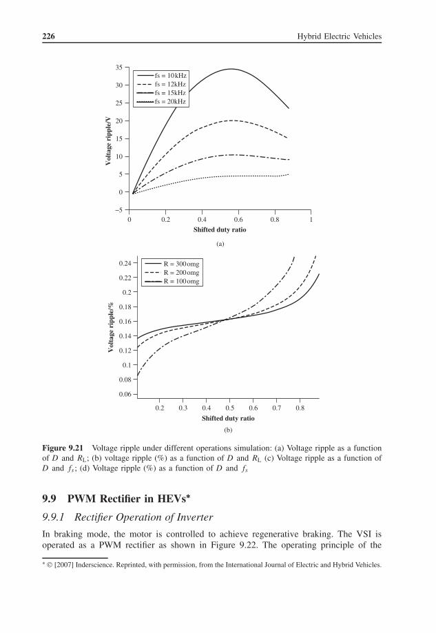
Therefore the voltage ripple is a function of D , R, and nV 1. This expression is applicableto both open-loop control and close-loop control. The condition of Equation 9.63 isV 2 > nV 1, which implies D(1 − D)RL > 2fsLs . From Equation 9.63, it is easy to see that�V2 is directly proportional to nV1/C. In order to further study the influential factors,the voltage ripple under different conditions is shown in Figure 9.21.
From Figure 9.21a, the absolute voltage ripple decreases when RL decreases under agiven D , and the ripple reaches a maximum at D = 0.5. However, in Figure 9.21b, therelative ripple is an increasing function of D and only reaches a maximum when D = 1.All the curves cross at D = 0.5.
When D < 0.5, a high resistance will result in a high ripple under a fixed D . WhenD > 0.5 the absolute ripple decreases with D for a given load resistance, but the relativeripple increases with D .
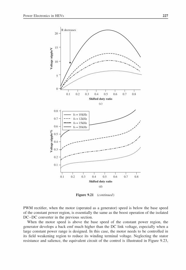
From Figure 9.21c,d, increasing the switching frequency is beneficial to limit both theabsolute ripple and the relative ripple of the output voltage.
226 Hybrid Electric Vehicles
0 0.2 0.4 0.6 0.8 1
Shifted duty ratio
35
30
25
20
15
10
5
0
−5
Vol
tage
rip
ple/
V
fs = 10kHzfs = 12kHzfs = 15kHzfs = 20kHz
0.2 0.40.3 0.6 0.70.5 0.8
Shifted duty ratio
0.24
0.22
0.2
0.18
0.16
0.14
0.12
0.1
0.08
0.06
Vol
tage
rip
ple/
%
R = 300omgR = 200omgR = 100omg
(a)
(b)
Figure 9.21 Voltage ripple under different operations simulation: (a) Voltage ripple as a functionof D and RL; (b) voltage ripple (%) as a function of D and RL (c) Voltage ripple as a function ofD and fs ; (d) Voltage ripple (%) as a function of D and fs
9.9 PWM Rectifier in HEVs∗
9.9.1 Rectifier Operation of Inverter
In braking mode, the motor is controlled to achieve regenerative braking. The VSI isoperated as a PWM rectifier as shown in Figure 9.22. The operating principle of the
∗ © [2007] Inderscience. Reprinted, with permission, from the International Journal of Electric and Hybrid Vehicles.
Power Electronics in HEVs 227
R decreases20
15
10
5
0
(c)
0.1 0.2 0.3 0.4 0.5 0.6 0.7 0.8
Shifted duty ratio
Vol
tage
nip
ple/
V
0.8
0.7
0.6
0.5
0.4
0.3
0.2
0.1
0.1 0.2 0.3 0.4 0.5 0.6 0.7 0.8
Shifted duty ratio
Vol
tage
nip
ple/
%
fs = 20kHzfs = 15kHzfs = 12kHzfs = 10kHz
(d)
Figure 9.21 (continued )
PWM rectifier, when the motor (operated as a generator) speed is below the base speedof the constant power region, is essentially the same as the boost operation of the isolatedDC–DC converter in the previous section.
When the motor speed is above the base speed of the constant power region, thegenerator develops a back emf much higher than the DC link voltage, especially when alarge constant power range is designed. In this case, the motor needs to be controlled inits field weakening region to reduce its winding terminal voltage. Neglecting the statorresistance and salience, the equivalent circuit of the control is illustrated in Figure 9.23,

228 Hybrid Electric Vehicles
Boost_3ph_avg
Bat
tery
−+
Us1
Us2
Us3
Us1
Us2
Us3
N
S
M
ω
Figure 9.22 PWM rectifier
Vvsi
Xq
Eo
(a)
(b) (c)
+
−
+
−
Eo
Vvsi
jIdXd
jIqXq
EoVvsi
jIdXd
jIqXq
Figure 9.23 Regenerative braking in the constant power region: (a) equivalent circuit; (b) phasordiagram at high speed in the constant power region; and (c) phasor diagram at lower speed in theconstant torque region
where E o is the induced back emf of the PM motor, Lq is the synchronous inductance,and V vsi is the equivalent sine wave output of the VSI:
Vvsi = Eo − jIqXq − jIdXd (9.64)
The purpose of the field weakening control is to achieve a constant V vsi for higher E o ,by applying a current opposite to the d-axis direction.
Power Electronics in HEVs 229
9.10 EV and PHEV Battery Chargers
The battery charging system is a critical part of EVs and PHEVs. The efficiency, chargingspeed, and cost of such chargers are crucial to the commercialization of PHEVs. Thereare many different topologies available for battery chargers. Due to safety requirementsand standards, most battery chargers are required to be isolated from the AC electric grid(such as requirement of SAE J1772). In some cases, bidirectional power flow is necessaryin order to realize vehicle-to-grid functions.
A survey conducted by the US Electric Power Research Institute (EPRI) revealed that78% of the US population drive 40 miles (64 km) or less in their daily commuting.Therefore, PHEVs capable of a 40 mile electric driving range can significantly reducegasoline usage in passenger cars. For a typical passenger vehicle (car and SUV), theaverage energy consumption is approximately 150–300 Wh per mile. To achieve a 40 mileelectric range, a battery that contains usable energy of 6–12 kWh is appropriate. Lithium-ion batteries are considered as the only viable energy storage solution for PHEVs at thetime being. To achieve safe and reliable operation while maintaining the cycle life andhealth of the batteries in a PHEV, the typical available energy from lithium-ion batteriesis approximately 60–70% of the nominal capacity. Therefore, a 10–16 kWh lithium-ionbattery pack is very typical in many PHEVs under development.
The battery onboard a PHEV needs to be charged from the grid through either anonboard or offboard charger. For private vehicles, these PHEVs will be charged at homeor a public charge station through either 110 or 220 V AC input. In order to make surethat the vehicle is ready for use by the second morning, the battery must be fully chargedwithin a reasonable amount of time, typically 2–8 hours.
In the past few decades, various charging circuits have been developed targeting dif-ferent applications, such as laptop computers, portable electronics, and uninterruptablepower supplies (UPSs). Isolation is one of the basic requirements for all battery chargersfor safety. The charging current is usually controlled by continuous feedback of criticalbattery parameters, such as battery voltage, the SOC, temperature, and so on. As far asthe unidirectional charging system is concerned, chargers based on flyback and forwardconverters are typical examples for low-power applications. Both topologies need onlyone active switch. However, flyback and forward converters undergo HV spikes when theexcessive energy stored in the leakage inductance of the isolation transformer is exhaustedat the turn-off moment. Therefore, at higher power operations, an auxiliary snubber cir-cuit is needed. Regardless of the limitations, flyback/forward topologies are being usedin PHEV chargers.
Chargers based on half-bridge and full-bridge unidirectional DC–DC converters arefavorable alternatives to chargers based on flyback and a forward converter. The magne-tization of the isolation transformer in a half-bridge converter is bidirectional, thereforethe demagnetizing circuit is eliminated. The leakage inductance of the transformer isa key parameter for energy transfer. The operation of a full-bridge DC–DC converteris similar to a half-bridge converter. The electrical stress of semiconductors in a half-bridge/full-bridge converter is significantly reduced. Soft switching is easy to implement inhalf-bridge/full-bridge converters. The disadvantages of these converters are the increasednumber of semiconductor switches.
230 Hybrid Electric Vehicles
Rectifier PFC DC-AC AC-DCAC
Figure 9.24 Basic PHEV charger architecture
Resonant converters can also be employed as battery chargers at extremely low cost.However, resonant chargers usually provide pulsed charge current, such as the case ininductive heating, other than constant current or constant voltage charging. The impact ofpulsed current charging on battery capacity and life cycle is not fully understood at thepresent time.
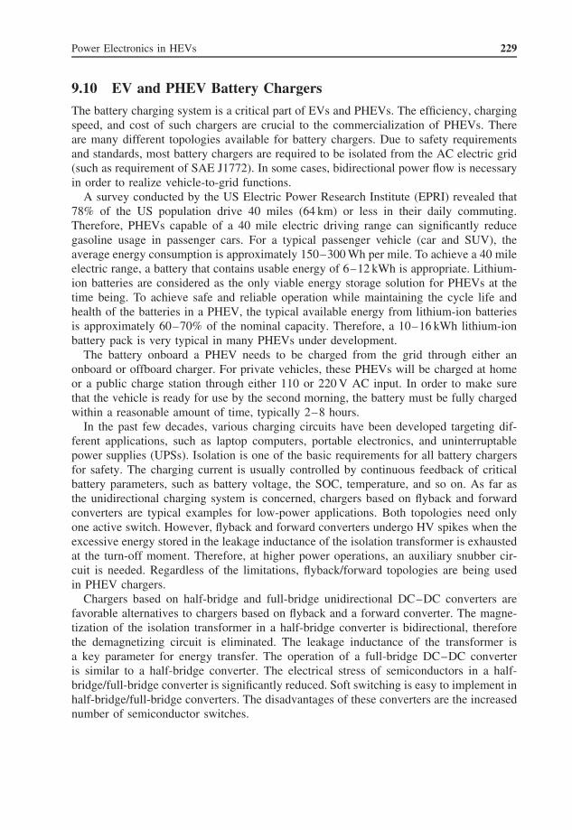
Figure 9.24 shows the general architecture of a unidirectional PHEV battery charger.It consists of a front-end rectifier, a power factor correction (PFC) stage, and an isolatedDC–DC stage.
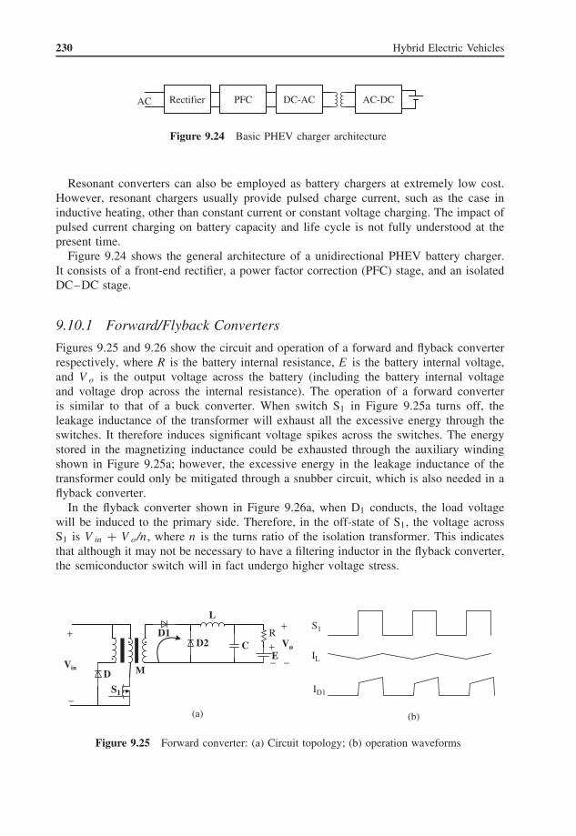
9.10.1 Forward/Flyback Converters
Figures 9.25 and 9.26 show the circuit and operation of a forward and flyback converterrespectively, where R is the battery internal resistance, E is the battery internal voltage,and V o is the output voltage across the battery (including the battery internal voltageand voltage drop across the internal resistance). The operation of a forward converteris similar to that of a buck converter. When switch S1 in Figure 9.25a turns off, theleakage inductance of the transformer will exhaust all the excessive energy through theswitches. It therefore induces significant voltage spikes across the switches. The energystored in the magnetizing inductance could be exhausted through the auxiliary windingshown in Figure 9.25a; however, the excessive energy in the leakage inductance of thetransformer could only be mitigated through a snubber circuit, which is also needed in aflyback converter.
In the flyback converter shown in Figure 9.26a, when D1 conducts, the load voltagewill be induced to the primary side. Therefore, in the off-state of S1, the voltage acrossS1 is V in + V o/n , where n is the turns ratio of the isolation transformer. This indicatesthat although it may not be necessary to have a filtering inductor in the flyback converter,the semiconductor switch will in fact undergo higher voltage stress.
. .D1
D2
L
C
M
S1
+
−
Vin
Vo
+
−E
+−
R
D
.
(a)
S1
IL
ID1
(b)
Figure 9.25 Forward converter: (a) Circuit topology; (b) operation waveforms

Power Electronics in HEVs 231
Vo
+
−E+−
+
−
Vin
.
.
D1RCD
snubber
S1
M
R S1
IS1
ID
(a) (b)
Figure 9.26 Flyback converters: (a) circuit topology; (b) operation waveforms
−Vo
+
−
E+
−
+
−
Vin
M
L
S1
S2
Vp
+
R
(a) (b)
S1
S2
Vp
Vin/2
−Vin/2
Vs1
Vin/2
Vin
Figure 9.27 Half-bridge converter: (a) circuit topology; (b) operation waveforms
9.10.2 Half-Bridge DC–DC Converter
Figure 9.27 shows a half-bridge DC–DC converter. Switches S1 and S2 are switchedwith their phase shifted by 180◦. The leakage inductance of the transformer serves asthe component for energy transfer. If the parasitic inductance of the commutating loop isnegligible, the voltage spike across the semiconductors will not be of concern.
9.10.3 Full-Bridge DC–DC Converter
Figure 9.28 shows the circuit topology and operation of a full-bridge DC–DC converter.Compared to the half-bridge converter where only half of the DC voltage is imposed on theprimary side of the transformer in every switching cycle, the full-bridge converter utilizesthe whole DC link voltage. Similar to a half-bridge converter, the leakage inductanceof the transformer in a full-bridge converter does not contribute to any voltage spike

232 Hybrid Electric Vehicles
S1S2
S3
S4
Vp
Ip
S1S2
S3
S4
Vp
Ip
Vo
+
−
E+
−
+
−
Vin Vp
+
−M
D5 D7
D6 D8
L
S2
S3
S4
S1
IpC
R
(a)
(b) (c)
Figure 9.28 Full-bridge converter: (a) circuit topology; (b) discontinuous mode operation; (c)continuous mode operation
across the switches. This leakage inductance should be designed appropriately for bestperformance [13].
9.10.4 Power Factor Correction Stage
A PFC stage is usually placed between the rectifier and the DC–DC stage to avoidharmonics pollution to the grid as well as to stabilize the DC link voltage. A typicalPFC circuit, shown in Figure 9.29, consists of an inductor L, an active switch S, and afreewheeling diode D. Bridgeless PFC circuits have also been used in battery chargers.
9.10.4.1 Decreasing Impact on the Grid
The AC grid side current with and without a PFC stage is shown in Figure 9.30, wherethe grid voltage is 110 V AC, and the output power of the charger is 5 kW.

Power Electronics in HEVs 233
RectifierAC Load
L
S
D
Figure 9.29 Power factor correction stage in a PHEV charger
Cur
rent
(A
)
Cur
rent
(A
)
0.020.0150.01 0.025 0.03
−100
−50
0
50
100
Time (s)
(a)
0.82 0.83 0.84 0.85
−40−30−20−10
01020304050
Time (s)
(b)
Figure 9.30 AC grid side current with and without PFC: (a) without PFC; (b) with a PFC
It can be seen from Figure 9.30 that with a PFC, the input current is much better. Thecurrent is close to sinusoidal and the current peak is significantly decreased. The impact ofharmonic currents on the grid is mitigated. Also the primary diode rectifier will undergosmaller current stress. The power factor is close to 1.
9.10.4.2 Decreasing the Impact on the Switches
The PFC circuit also helps boost the DC link voltage to a higher level and stabilize the DClink voltage. Therefore, at the same output power, the current through the switches will bedecreased to enhance safety and output capability. Figure 9.31a shows the switch current atdifferent V in with the same output power. When V in is increased to 400 V DC, the switchcurrent is significantly decreased. As long as the voltage across the switches does notexceed the breakdown value, higher DC bus voltage will lead to higher power capabilityfor the same devices used. Figure 9.31b shows the maximum charging current that thesystem can deliver. Increasing the DC link voltage will benefit the output capability.Here the maximum repetitive switched-off current of the semiconductor switch is setto 70 A.

234 Hybrid Electric Vehicles
Cur
rent
(A
)
Cha
rgin
g cu
rren
t (A
)
5.54 5.56 5.58 5.6
−100
−50
0
50
100
Vin = 400VVin = 150V
Times (ms)
(a)
50 150 250 3500
5
10
15
20
25
30
Battery voltage (V)
350V, n = 1.5300V, n = 1.5150V, n = 3
(b)
Figure 9.31 Comparison of the switch current without PFC: (a). comparison of switch current;(b) Maximum charging current under different Vin
Vo
Vs = 110V
2 VoltageSensors
2 CurrentSensors
C2
C1L2
K1
R K2
K3
Choke
Fuse
IsolationTransformer
Figure 9.32 Isolation using a high-frequency transformer
9.10.5 Bidirectional Battery Chargers
It is possible to equip a PHEV with a bidirectional charger. With bidirectional powertransfer capability, the energy stored in a PHEV battery can be sent back to the gridduring peak demand hours for peak shaving of the AC electric grid, or to supply powerto the home and office during a power outage.
The isolation can be achieved using high-frequency transformers in the DC–DC stageat high-frequency level as shown in Figure 9.32. The isolation can also be achieved usinga transformer at the grid frequency level as shown in Figure 9.33. It is difficult to add aPFC stage to the bidirectional chargers but the AC side current can be controlled usingthe grid side inverter to limit the harmonics and improve power factor.
9.10.6 Other Charger Topologies
The above chargers are based on single-phase low-power inputs. In applications suchas commercial transportation and recharge stations, it is necessary to quickly charge the

Power Electronics in HEVs 235
VoVs = 110V
2 VoltageSensors
2 CurrentSensors
C2
C1L2
K1
R K2
K3Choke
Fuse
IsolationTransformer
Figure 9.33 Isolation at the grid level with a line frequency transformer
battery in a relatively short time. For example, for a 16 kWh pack, to charge the batteryfrom 30 to 80% SOC in 5 minutes will require 16 kWh × (80% – 30%)/(5/60) = 96 kW.Assuming that the battery is able to accept this type of charging, the charging power willhave to be supplied. This is typically done through a three-phase high-power input.
Excessive heat may be generated during high-power fast charging of EV and PHEVbatteries. The high charge rate may also impact the long-term capacity or life of the battery.
With more and more renewable energy and distributed generation, DC grids are startingto emerge. Almost all renewable sources, including solar and wind, can be in the form ofDC. If a PHEV is connected to a DC grid, then the battery can be charged directly fromthe DC source. Traditional chargers designed for AC input can be used to take DC input,but a specially designed DC charger will have no need for the rectifier and PFC stage.
9.10.7 Inductive Charging
The above chargers all need an electrical contact with the electric outlet. This hard-wiredelectrical connection can provide a few caveats. For example, if the cable is pulled outof the electric outlet (whether intentional or unintentional) when the battery is still beingcharged, then there could be a spark and potential damage or injury. Another example isif somebody (such as children) could get hurt if they happen to play with the cords etc.Charging the vehicle when it is raining could be potentially dangerous. Wear and tear ofthe plug and cable could also be a source of danger.
Hence inductive charging becomes an alternative. In 1995, the US SAE Electric Vehi-cle Charging System Group, Japanese manufacturers including Toyota, Nissan, Honda,and DENSO, and IEC/ISO together developed the inductive charging standard SAEJ1773. In 1999, SAE J1773 was enacted and recommended as an international standard(http://www.toyota.com). GM has already produced electric vehicles adopting inductivecharging in GM’s EV1 program in the 1990s. Since inductive charging does not involvedirect contact of electricity, it is a safe and convenient way to charge an EV battery. Thetask can even be completed by a child for 50 kW inductive charging.
Inductive charging involves an isolation transformer where the secondary winding andcore can be removed from the primary. Figure 9.34 shows the topology used in induc-tive chargers.

236 Hybrid Electric Vehicles
AC DiodeRectifier
H-bridgeInverter
Full-bridge
Rectifier...
coupler
sensor
communicationRF
EMIDepressor PFC
+−
+−
Figure 9.34 Isolated inductive charger
Source of power
Parked CarReceiver
Figure 9.35 Wireless charging of a PHEV/EV on a parking floor
9.10.8 Wireless Charging
Wireless charging involves the use of power and energy transfer at a much longer distance.It is different from inductive charging which involves a transformer with closely placedprimary and secondary windings. Although inductive charging can eliminate the directelectric contact, it still needs a plug, cable, and physical connection of the inductivecoupler. Wear and tear of the plug and cable could cause danger as well.
Wireless charging could eliminate the cable and plug altogether. In this scenario, adriver can pull the car over to a specially designed parking lot and the car battery isautomatically charged without the pulling of any cable or plug as shown in Figure 9.35.It provides the safest approach for EV battery charging.
There have been a few different experiments carried out for wireless energy transfer. Themost promising technology is using electromagnetic resonance as shown in Figure 9.36.In this setup, there is a pair of antennas with one placed in the parking structure asthe transmitter and one inside the car as the receiver. The two antennas are designed toresonate at the controlled frequency. The limitations are the level of power transfer, andefficiency due to the large air gap between the two antennas.
In the circuit shown in Figure 9.35, Rs is the internal impedance of the source and theresistance of the primary coil, Ro is the load resistance and the resistance of the secondarycoil, Ll is the leakage inductance of the each coil, and Lm is the mutual inductance of thetwo coils. There are two ways to make the circuit resonant. If we design the circuit andselect the frequency of the power supply V 1 such that
ωLl − 1
ωC= −2ωLm (9.65)

Power Electronics in HEVs 237
V1
L1
Lm
L1_C1 C2
Ro
Rs
V1 RoLm
Rs
V1 RoLm
Rs −2Lm −2Lm
+
−
+
−
+
−
(a)
(b) (c)
Figure 9.36 Circuits for electromagnetic resonance-based wireless charging: (a) circuit; (b) equiv-alent circuit at resonance frequency condition 1; (c) equivalent circuit at resonance frequency atcondition 2
and the total equivalent impedance is
Z = Rs − jωLmRo
Ro − jωLm
(9.66)
If we design
ωLl − 1
ωC= 0 (9.67)
and the total equivalent impedance is
Z = Rs + jωLmRo
jωLm + Ro
(9.68)
then the circuit will be in resonant. However, since both the mutual inductance and leakageinductance change with distance between the two coils, the frequency will have to betuned based on the distance in real-world applications. Figure 9.36b,c shows the equivalentcircuit during resonance of the two conditions. Figure 9.37 shows the simulation results ofthe circuit. The first plot shows two resonant frequencies. The second plot shows that whenthe distance between the two coils increases, the two resonant frequencies gets closer.
9.11 Modeling and Simulation of HEV Power Electronics
Modeling and simulation play important roles in the design and development of powerelectronics circuits. The simulation of power electronics circuits in hybrid vehicle

238 Hybrid Electric Vehicles
Frequency
1.0MHz 3.0MHz 10MHz 30MHz 100MHz0V
20V
40V
60V
80V
100V
V(Ro:1)V(Ro:1)
Frequency
1.0MHz 3.0MHz 10MHz 30MHz 100MHz
V(Ro:1)
0V
20V
40V
60V
80V
100V
120V
Figure 9.37 Resonance frequency of the wireless charging circuit: top, output voltage for shorterdistance; bottom: output voltage for longer distance
applications can be divided into two categories: device-level simulations and system-levelsimulations [11, 25–29].
9.11.1 Device-Level Simulation
Device-level simulation can reveal the details of the device behavior. To obtain detailedloss data, overvoltages, and other component stresses due to the non-ideal nature ofpower electronics devices, and the stray inductance and capacitance of the circuitry, it isnecessary to simulate a number of cycles of detailed switching pertaining to the worstcase scenario.

Power Electronics in HEVs 239
PWM
+
−
C3 R4Vd+
−
Averagebuck
model
(a)
(b)
Figure 9.38 Device-level and system-level modeling of a buck converter. (a) System-level modelonly taking into account the non-linear characteristics of the inductor. (b) Device-level modelinvolving detailed switching of the MOSFET
9.11.2 System-Level Model
Detailed device-level simulation can take a significant amount of time due to the highswitching frequency used in the power electronics circuits, whereas the mechanical con-stants of the vehicle system could be a few seconds or more. Therefore, device-levelsimulation, although can simulate the dynamic performance of the circuit, is not suitablefor simulating the vehicle performance, such as gradability, acceleration, and fuel econ-omy. On the other hand, the electronics circuits have very fast transients, when comparedto the vehicle dynamics.
In system-level simulations, the average model is generally used. For example, abuck converter can be represented in the simulation by an average model as shownin Figure 9.38a. A simulation of the system performance of one second only takes twoseconds of simulation time, whereas in Figure 9.38b, which uses detailed device-levelmodels, it takes about 20 minutes to obtain the system performance of one second.
9.12 Emerging Power Electronics Devices
The present silicon (Si) technology is reaching the material’s theoretical limits and can-not meet all the requirements of hybrid vehicle applications in terms of compactness,light weight, high power density, high efficiency, and high reliability under harsh con-ditions. New semiconductor materials, such as silicon carbide (SiC), for power deviceshave the potential to eventually overtake Si power devices in hybrid vehicle powertrainapplications [30–37].
SiC power devices potentially have much smaller switching and conduction losses andcan operate at much higher temperature than comparable Si power devices. Hence, aSiC-based power converter will have a much higher efficiency than that of convertersbased on Si power devices if the same switching frequency is used. Alternatively, a

240 Hybrid Electric Vehicles
higher switching frequency can be used to reduce the size of the magnetic componentsin a SiC-based power converter. In addition, because SiC power devices can be operatedat much higher temperatures without much change in their electrical properties, ease ofthermal management and high reliability can be achieved.
9.13 Circuit Packaging
Electromagnetic interference (EMI) is one of the most challenging problems in powerelectronics circuits. The high switching frequency and high current generate electromag-netic fields that will permeate the other components in the vehicle system and create largeelectrical noise. In order to minimize EMI, components must be carefully placed so thatEMI is not contained by shielding and will have minimal effect on the rest of the system.All paths must be kept as close as possible so that the generated fields will nullify oneanother. To minimize parasitics and aid in the EMI issue, the lengths of wires need to bekept as short as possible.
The control circuit needs to provide protection for overcurrent, short circuit, overvolt-age, and undervoltage. The capability to detect any fault signal and turn off the gate drivesignals to the primary switches is a critical part of power electronic circuit design. Fastfuses need to be used in the circuit to protect the converter from being damaged by anyother faults and used for safety.
9.14 Thermal Management of HEV Power Electronics∗
At power levels of 100 kW, even with an efficiency of 96–98%, the power losses of eachpower electronic unit is 2–4 kW. With two or three powertrain motors and associatedpower electronics circuits, together with the high-power bidirectional DC–DC converter,the heat generated in the hybrid vehicle system could be significant.
Significant advances in the thermal management of both power electronics and motorsfor HEV propulsion system must be achieved to meet the automotive industry’s goalsof reduced weight, volume, and cost [37–40]. Through the optimization of existingtechnologies and the expansion of new pioneering cooling methods, higher powerdensities, smaller volumes, and increased reliabilities can be realized in the hybridpowertrain components. Investigations and advances in thermal issues can provide aviable path to bridging gaps still plaguing the successful achievement of automotivetechnical targets while simultaneously enhancing the ability to apply new technologiesin automotive applications as they mature.
Thermal performance of a power module is measured by the maximum temperaturerise in the die at a given power dissipation level with a fixed heat sink temperature. Thelower the die temperature, the better the electrical performance. As the thermal resistancefrom the junction of the die to the heat sink is reduced, higher power densities can beachieved for the same temperature rise, or for the same power density a lower junctiontemperature can be attained. It is important to reduce thermal cycling or maintain lowambient temperature to improve the life and reliability of the die.
The main areas of concern in thermal management of power electronics are: operatingtemperature of IGBTs (it should be less than 125 ◦C); contact resistance between various
∗ © [2007] Inderscience. Reprinted, with permission, from the International Journal of Electric and Hybrid Vehicles.

Power Electronics in HEVs 241
0.01
0.1
1
10
100
1000
1 10 100 1000
Temperature difference, °C
Hea
t flu
x, W
/cm
2
air, forced convection
h ~ 0.01 W/cm2 °C
Liquid, forced convection
h ~ 1 W/cm
2 °Ctwo phase boilin
g
h ~ 10 W/cm
2 °C
variousworking
fluids undervarying
pressures
Liquid, Natural
Convection
h ~ 0.1 W/cm °C
2 phase jet imping., sp
ray,
high conductivity thermal
grease, heat spreaders
Figure 9.39 Existing cooling technologies
layers of a power module; low-thermal-conductivity thermal paste; heat flux limitations(ideally, faster IGBTs would have to reject heat at a rate of 250 W/cm2); limitations onthe inlet cooling fluid temperature (it is desirable to use the engine coolant at 105 ◦C);the cost of the cooling system; weight and volume.
The existing cooling technologies are depicted in Figure 9.39. It is shown that con-ventional cooling techniques such as forced convection and simple two-phase boilingtechniques are not capable of removing high heat fluxes (in the range of 250 W/cm2) atlow temperature differences (20 ◦C). However, this figure shows clearly that employmentof enabling technologies such as spray cooling and jet impingement along with someother innovative improvements will be able to meet the goals of the automotive industry.
Ideally, it would be more beneficial if IGBTs could be designed to operate at highertemperatures. The industry is pursuing various long-term research projects to evaluate andachieve that objective. However, to meet the immediate need of the automotive industry,existing IGBTs should be operated at temperatures below 125 ◦C.
The existing power modules are constructed by bonding together the die, copper layers,substrate, and the base plate. The whole module is then mounted on a heat sink usingthermal grease or thermal pad. The existing thermal greases used by the industry that canstand high temperatures have very low conductivities on the order of 0.3–0.5 W/(m K).As a result of this low thermal conductivity, the thermal grease constitutes 30–40% ofthe total thermal resistance between the junction and the heat sink. Therefore it is crucialto reduce this resistance by increasing the thermal conductivity of the thermal grease.Figure 9.40 shows the impact of the conductivity of the thermal grease on the overalltemperature difference between the junction and the heat sink. For a thermal conductivityof 0.5 W/(m K), the temperature difference is about 65 ◦C. If the thermal conductivity ofthe thermal grease is doubled to 1.0 W/(m K), the maximum temperature difference canbe reduced to 35 ◦C.
To improve the power density of power modules, higher heat fluxes should be removedfrom the module because of increased switching frequencies. An important approach for

242 Hybrid Electric Vehicles
0
10
20
30
40
50
60
70
80
0.1 1 10 100 1000Thermal conductivity, W/m K
Tem
pera
ture
dif
fere
nce,
°C
Figure 9.40 Impact of thermal interface material conductivity on temperature difference
removing higher heat fluxes from the IGBTs is to spread out their heat flux over a largersurface. The exiting copper or aluminum base plates spread the heat 20–30%, reducingthe maximum heat flux by a corresponding amount. Use of more effective heat spreaderssuch as highly conductive metal layers, mini-heat pipes, and/or phase change materialsinside the cold plate can spread out the high heat flux of the IGBTs over a larger surfacearea and reduce the maximum heat flux that needs to be removed by as much as 40%.This is a reduction of 50% in the maximum heat flux that needs to be removed and thisrequirement can be easily met by one of the enabling cooling technologies such as jetimpingement and spray cooling currently being considered. Figure 9.41 shows the effectof utilizing a heat spreader that results in an additional 4–6 ◦C reduced temperature atthe junction.
Semikron plate thickness influence, 84 W/cm2, Al plate, jet impingement
0.00
2.00
4.00
6.00
8.00
10.00
12.00
14.00
16.00
18.00
20.00
0 1 2 3 4 5 6 7 8 9Plate thickness (mm)
Ove
rall
delta
-T (
°C)
Existing base plate
Base plate withheat spreader
Figure 9.41 The impact of utilizing heat spreaders on junction temperature

Power Electronics in HEVs 243
One approach to maintaining the power module’s temperature at 125 ◦C or below is toprovide a separate cooling loop where the coolant can enter the heat sink at temperatures aslow as 85 ◦C, hence providing an adequate temperature difference to maintain the IGBTs’temperature at the desired value while removing heat fluxes as high as 250 W/cm2.
9.15 Conclusions∗
This chapter presented an overview of the power electronics circuits for HEV applicationswith a focus on special circuit topologies, analysis, and thermal management. Novel powerswitching devices and power electronics systems have the potential to improve the overallperformance of hybrid vehicles. Continued effort in power electronics circuit research anddevelopment will most likely be focused on innovative circuit topologies, optimal control,novel switching devices, and novel thermal management methods.
References1. Bose, B.K. (2000) Energy, environment, and advances in power electronics. Proceedings of the International
Symposium on Industrial Electronics, December, Vol. 1, pp. TU1–T14.2. Jahns, T.M. and Blasko, V. (2001) Recent advances in power electronics technology for industrial and
traction machine drives. Proceedings of the IEEE , 89, 963–975.3. Miller, J.M. (2003) Power electronics in hybrid electric vehicle applications. Proceedings of the 18th
Applied Power Electronics Conference, February, Vol. 1, pp. 23–29.4. Ehsani, M., Rahman, K.M., and Toliyat, H.A. (1997) Propulsion system design of electric and hybrid
vehicles. IEEE Transactions on Industrial Electronics , 44, 19–27.5. Rahman, M.F. (2004) Power electronics and drive applications for the automotive industry, Proceedings
of the Power Electronics Systems and Applications Conference, November, pp. 156–164.6. Rajashekara, K. (2003) Power electronics applications in electric/hybrid vehicles. Proceedings of
IECON’03, November, Vol. 3, pp. 3029–3030.7. Emadi, A., Williamson, S.S., and Khaligh, A. (2006) Power electronics intensive solutions for advanced
electric, hybrid electric, and fuel cell vehicular power systems. IEEE Transactions on Power Electronics ,21, 567–577.
8. Hamilton, D.B. (1996) Electric propulsion power system - overview, Power Electronics in Transportation,pp. 21–28.
9. Vezzini, A. and Reichert, K. (1996) Power electronics layout in a hybrid electric or electric vehicle drivesystem. Power Electronics in Transportation, pp. 57–63.
10. Emadi, A., Ehsani, M., and Miller, J.M. (1999) Advanced silicon rich automotive electrical power systems.Proceedings of the Digital Avionic Systems Conference, October, Vol. 2, 8.B.1-1–8.B.1-8.
11. Amrhein, M. and Krein, P.T. (2005) Dynamic simulation for analysis of hybrid electric vehicle systemand subsystem interactions, including power electronics. IEEE Transactions on Vehicular Technology , 54,825–836.
12. Namuduri, C.S. and Murty, B.V. (1998) High power density electric drive for an hybrid electric vehicle.Proceedings of the 13th Applied Power Electronics Conference, February, Vol. 1, pp. 34–40.
13. Xingyi, Xu (1999) Automotive power electronics - opportunities and challenges [for electric vehicles].International Conference on Electric Machines and Drives, May, pp. 260–262.
14. Ehsani, M., Rahman, K.M., Bellar, M.D., and Severinsky, A. (2001) Evaluation of soft switching for EVand HEV motor drives. IEEE Transactions on Industrial Electronics , 48 (1), 82–90.
15. Marei, M.I., Lambert, S., Pick, R. et al. (2005) DC/DC converters for fuel cell powered hybrid electricvehicle. Vehicle Power and Propulsion Conference, September, pp. 126–129.
16. Katsis, D.C. and Lee, F.C. (1996) A single switch buck converter for hybrid electric vehicle generators.Power Electronics in Transportation, pp. 117–124.
∗ © [2007] Inderscience. Reprinted, with permission, from the International Journal of Electric and Hybrid Vehicles.

244 Hybrid Electric Vehicles
17. Chan, C.C., Chau, K.T., Jiang, J.Z. et al. (1996) Novel permanent magnet motor drives for electric vehicles.IEEE Transactions on Industrial Electronics , 43, 331–339.
18. Hayes, J.G. and Egan, M.G. (1999) A comparative study of phase-shift, frequency, and hybrid controlof the series resonant converter supplying the electric vehicle inductive charging interface. 14th AppliedPower Electronics Conference, March, Vol. 1, 450–457.
19. Krein, P.T., Roethemeyer, T.G., White, R.A., and Masterson, B.R. (1994) Packaging and performance ofan IGBT-based hybrid electric vehicle. Power Electronics in Transportation, pp. 47–52.
20. Ehsani, M., Rahman, K.M., Bellar, M.D., and Severinsky, A.J. (2001) Evaluation of soft switching for EVand HEV motor drives. IEEE Transactions on Industrial Electronics , 48, 82–90.
21. Tolbert, L.M., Peng, F.Z., and Habetler, T.G. (1998) Multilevel inverters for electric vehicle applications.Power Electronics in Transportation, pp. 79–84.
22. Di Napoli, A., Crescimbini, F., Rodo, S. et al. (2002) Multiple input DC-DC power converter for fuel-cellpowered hybrid vehicles. 33rd Power Electronics Specialists Conference, June, pp. 1685–1690.
23. Solero, L., Lidozzi, A., and Pomilio, J.A. (2005) Design of multiple-input power converter for hybridvehicles. IEEE Transactions on Power Electronics , 20, 1007–1016.
24. Gargies, S., Wu, H., and Mi, C. (2006) Isolated bidirectional DC/DC converter for hybrid electric vehicleapplications. 6th Intelligent Vehicle Symposium, June.
25. Onoda, S. and Emadi, A. (2004) PSIM-based modeling of automotive power systems: conventional, electric,and hybrid electric vehicles. IEEE Transactions on Vehicular Technology , 53, 390–400.
26. Williamson, S., Lukic, M., and Emadi, A. (2006) Comprehensive drive train efficiency analysis of hybridelectric and fuel cell vehicles based on motor-controller efficiency modeling. IEEE Transactions on PowerElectronics , 21, 730–740.
27. Filippa, M., Chunting, M., Shen, J. et al. (2005) Modeling of a hybrid electric vehicle powertrain test cellusing bond graphs. IEEE Transactions on Vehicular Technology , 54, 837–845.
28. Mi, C., Hui, L., and Yi, Z. (2005) Iterative learning control of antilock braking of electric and hybridvehicles. IEEE Transactions on Vehicular Technology , 54, 486–494.
29. Hak-Geun, J., Bong-Man, J., Soo-Bin, H. et al. (2000) Modeling and performance simulation of powersystems in fuel cell vehicle. Proceedings of IPEMC 2000, August, 2, 671–675.
30. Johnson, R.W., Evans, J.L., Jacobsen, P. et al. (2004) The changing automotive environment: high-temperature electronics. IEEE Transactions on Electronics Packaging Manufacturing , 27, 164–176. Seealso IEEE Transactions on Components, Packaging and Manufacturing Technology, Part C: Manufacturing .
31. Ozpineci, B., Tolbert, L.M., Islam, S.K. et al. (2001) Effects of silicon carbide (SiC) power devices onHEV PWM inverter losses. 2, 1061–1066.
32. Kelley, R., Mazzola, M.S., and Bondarenko, V. (2006) A Scalable SiC Device for DC/DC Converters inFuture Hybrid Electric Vehicles, p. 4.
33. Ozpineci, B., Tolbert, L.M., Islam, S.K. et al. (2002) Testing, characterization, and modeling of SiC diodesfor transportation applications. 33rd Power Electronics Specialists Conference, June, pp. 1673–1678.
34. Dreike, P.L., Fleetwood, D.M., King, D.B. et al. (1994) An overview of high-temperature electronic devicetechnologies and potential applications. IEEE Transactions on Components, Packaging, and ManufacturingTechnology, Part A, 17, 594–609. [see also IEEE Transactions on Components, Hybrids, and ManufacturingTechnology].
35. Ozpineci, B., Chinthavali, M.S., and Tolbert, L.M. (2005) A 55 kW three-phase automotive traction inverterwith SiC Schottky diodes. Vehicle Power and Propulsion Conference, September, p. 6.
36. Ohashi, H. (2003) Power electronics innovation with next generation advanced power devices. InternationalTelecommunications Energy Conference, October, pp. 9–13.
37. Traci, R.M., Acebal, R., and Mohler, T. (1999) Integrated thermal management of a hybrid electric vehicle.IEEE Transactions on Magnetics , 35, 479–483.
38. Alaoui, C. and Salameh, Z.M. (2005) A novel thermal management for electric and hybrid vehicles. IEEETransactions on Vehicular Technology , 54, 468–476.
39. White, S.B., Gallego, N.C., Johnson, D.D. et al. (2004) Graphite foam for cooling of automotive powerelectronics. Power Electronics in Transportation, pp. 61–65.
40. Tatoh, N., Hirose, Y., Nagai, M. et al. (2000) Thermal management analysis of high-power electronicmodules using Cu bonded AlN substrates. International Conference on Thermal and ThermomechanicalPhenomena in Electronic Systems, May, Vol. 2, pp. 297–302.


![[XLS]A Revenue... · Web view40435 MD-HEVS Health Res & Outcomes Eval 110131 MD-HEVS Connors ARDS 110661 MD-HEVS Stukenborg AHRQ R01 Stukenborg, George J 110696 MD-HEVS Kilbridge](https://img.pdfslide.us/doc/110x75/5b2586e97f8b9a353f8b4fa8/xls-ampa-revenue-web-view40435-md-hevs-health-res-outcomes-eval-110131.jpg)