Embed Size (px)
Citation preview
Hybrid CMOS/Nanodevice Circuits for
High Throughput Pattern Matching Applications
Fabien Alibart1, Timothy Sherwood
2, and Dmitri B. Strukov
1*
1 Electrical and Computer Engineering Department, University of California Santa Barbara
2 Computer Science Department, University of California Santa Barbara
*Email: [email protected]
Abstract
We propose a class of novel hybrid CMOS/nanodevice
circuits for pattern matching applications (e.g. real-time
network intrusion detection, network packet routing, DNA
sequencing), with the potential for dramatic
improvements in throughput, density, and power
performance relative to state-of-the-art designs. The
performance advantage of our novel circuits is mainly
due to three factors: the implementation of a ternary
content addressable memory cell with stackable ultra-
dense resistive switching (“memristive” or RRAM)
devices; three dimensional hybrid CMOS/nanodevice
circuitry with an area-distributed interface enabling high
communication bandwidth between the memory and
CMOS subsystems; and use of a modified CMOL FPGA
fabric with low reconfiguration overhead.
1. Introduction
Pattern matching is a bottleneck operation in many
important applications including network intrusion
detection, network packet routing, DNA sequence
matching, database searching, spell checking, spam
filtering, and some image and signal processing tasks [1].
The primary performance metric for pattern matching
tasks is typically throughput, which, for example, would
be required to match the speed of communication
network. Of course it makes little sense to discuss
performance alone, and both energy per matching
operation and latency are also important metrics in this
space, (e.g. to enable fast and low power DNA
sequencing [2] or minimize link delay in a filtering
system).
At a high level, contemporary high performance
approaches can be divided into two groups. The first
approach makes use of the reconfigurable nature of field
programmable gate arrays (FPGA), exploiting the fine
grain configurability of the devices to implement a dense
pattern matching structure [1-6]. For example, many
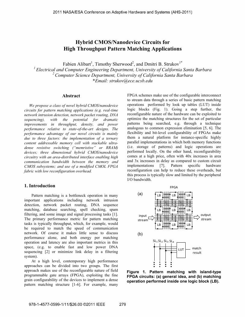
FPGA schemes make use of the configurable interconnect
to stream data through a series of basic pattern matching
operations performed by look up tables (LUT) inside
logic blocks (Fig. 1). Going a step further, the
reconfigurable nature of the hardware can be exploited to
optimize the matching structures for the set of particular
patterns being searched, e.g. through a technique
analogous to common expression elimination [5, 6]. The
flexibility and bit-level configurability of FPGAs make
them a natural platform for instance-specific highly
parallel implementations in which both memory functions
(i.e. storage of patterns) and logic operations are
performed locally. On the other hand, reconfigurability
comes at a high price, often with 40x increases in area
and 3x increases in delay as compared to custom circuit
implementations [7]. Pattern specific hardware
reconfiguration can help to reduce these overheads, but
this process is typically slow and limited by the peripheral
I/O bandwidth.
match result
LUT
SL1 SL2 SL3 SL4
(a) LB
LB
LBLBLB
LB
LB LB
LB
(b)
FPGA
output stream
inputstream
Figure 1. Pattern matching with island-type FPGA circuits: (a) general idea, and (b) matching operation performed inside one logic block (LB).
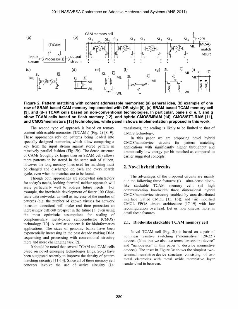
The second type of approach is based on ternary
content addressable memories (T/CAMs) (Fig. 2) [8, 9].
These approaches rely on patterns being loaded into
specially designed memories, which allow comparing a
key from the input stream against stored pattern in
massively parallel fashion (Fig. 2b). The dense structure
of CAMs (roughly 2x larger than an SRAM cell) allows
more patterns to be stored in the same unit of silicon,
however the long memory lines used for matching must
be charged and discharged on each and every search
cycle, even when no matches are to be found.
Though both approaches are somewhat satisfactory
for today’s needs, looking forward, neither approach will
scale particularly well to address future needs. For
example, the inevitable development of faster 100 Gbps-
scale data networks, as well as increase of the number of
patterns (e.g. the number of known viruses for network
intrusion detection) will make real time protection an
increasingly difficult prospect in the future [5] even using
the most optimistic assumptions for scaling of
complementary metal-oxide semiconductor (CMOS)
technology [10]. A similar concern is for bioinformatics
applications. The sizes of genomic banks have been
exponentially increasing in the past decade making DNA
sequencing and processing with conventional circuitry
more and more challenging task [2].
It should be noted that several TCAM and CAM cells
based on novel emerging technologies (Figs. 2c-g) have
been suggested recently to improve the density of pattern
matching circuitry [11-14]. Since all of these memory cell
concepts involve the use of active circuitry (i.e.
transistors), the scaling is likely to be limited to that of
CMOS technology. In this paper we are proposing novel hybrid
CMOS/nanodevice circuits for pattern matching
applications with significantly higher throughput and
dramatically low energy per bit matched as compared to
earlier suggested concepts.
2. Novel hybrid circuits
The advantages of the proposed circuits are mainly
due the following three features: (i) ultra-dense diode-
like stackable TCAM memory cell; (ii) high
communication bandwidth three dimensional hybrid
CMOS/nanodevice circuitry enabled by area-distributed
interface (called CMOL [15, 16]); and (iii) modified
CMOL FPGA circuit architecture [17-19] with low
reconfiguration overhead. Let us now discuss more in
detail these features.
2.1. Diode-like stackable TCAM memory cell
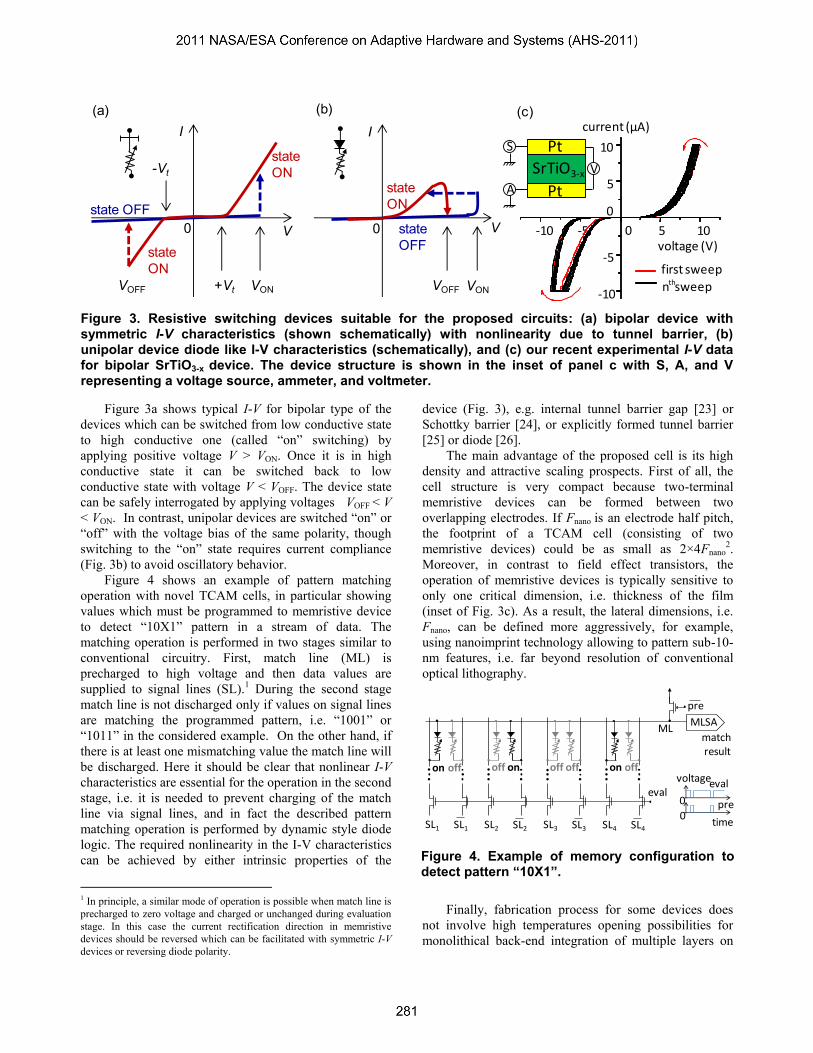
Novel TCAM cell (Fig. 2i) is based on a pair of
nonlinear resistive switching (“memristive” [20-22])
devices. (Note that we also use terms “crosspoint device”
and “nanodevice” in this paper to describe memristive
devices). The inset in Figure 3c shows the simplest two-
terminal memristive device structure consisting of two
metal electrodes with metal oxide memristive layer
sandwiched in between.
match result
MLSA
preSL1 SL2 SL3 SL4SL1 SL2 SL3 SL4
ML
(a)
SL SLML
(c)
(b)
ML
WL
SL SLML
SL SLML
WL
SL SL(d) (e) (f) (g)
ML
WL
SL SL(i)
MLSL SL
(T)CAM
Processor(s)output stream
inputstream
CAM memory cell
Figure 2. Pattern matching with content addressable memories: (a) general idea, (b) example of one row of SRAM-based CAM memory implemented with OR style [9], (c) SRAM-based TCAM memory cell [9], and (d-i) TCAM cells based on non-conventional technologies. In particular, panels d, e, f, and g show TCAM cells based on flash memory [12], and hybrid CMOS/MRAM [14], CMOS/STT-RAM [11], and CMOS/memristors [13] technologies, while panel i shows implementation proposed in this work.
V
I
(a)
state
ON
state
ON
0
+Vt
state OFF
VONVOFF
-Vt
V
I
(b)
state
ON
0 state
OFF
VONVOFF
(c)
Pt
Pt
SrTiO3-x
S
A
V
-10 -5 0 5 10
-10
-5
0
5
10
nthsweep
current (μA)
voltage (V)
first sweep
Figure 3. Resistive switching devices suitable for the proposed circuits: (a) bipolar device with symmetric I-V characteristics (shown schematically) with nonlinearity due to tunnel barrier, (b) unipolar device diode like I-V characteristics (schematically), and (c) our recent experimental I-V data for bipolar SrTiO3-x device. The device structure is shown in the inset of panel c with S, A, and V representing a voltage source, ammeter, and voltmeter.
Figure 3a shows typical I-V for bipolar type of the
devices which can be switched from low conductive state
to high conductive one (called “on” switching) by
applying positive voltage V > VON. Once it is in high
conductive state it can be switched back to low
conductive state with voltage V < VOFF. The device state
can be safely interrogated by applying voltages VOFF < V
< VON. In contrast, unipolar devices are switched “on” or
“off” with the voltage bias of the same polarity, though
switching to the “on” state requires current compliance
(Fig. 3b) to avoid oscillatory behavior.
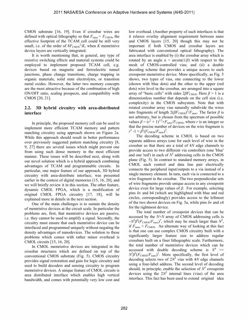
Figure 4 shows an example of pattern matching
operation with novel TCAM cells, in particular showing
values which must be programmed to memristive device
to detect “10X1” pattern in a stream of data. The
matching operation is performed in two stages similar to
conventional circuitry. First, match line (ML) is
precharged to high voltage and then data values are
supplied to signal lines (SL).1 During the second stage
match line is not discharged only if values on signal lines
are matching the programmed pattern, i.e. “1001” or
“1011” in the considered example. On the other hand, if
there is at least one mismatching value the match line will
be discharged. Here it should be clear that nonlinear I-V
characteristics are essential for the operation in the second
stage, i.e. it is needed to prevent charging of the match
line via signal lines, and in fact the described pattern
matching operation is performed by dynamic style diode
logic. The required nonlinearity in the I-V characteristics
can be achieved by either intrinsic properties of the
1 In principle, a similar mode of operation is possible when match line is
precharged to zero voltage and charged or unchanged during evaluation
stage. In this case the current rectification direction in memristive
devices should be reversed which can be facilitated with symmetric I-V
devices or reversing diode polarity.
device (Fig. 3), e.g. internal tunnel barrier gap [23] or
Schottky barrier [24], or explicitly formed tunnel barrier
[25] or diode [26].
The main advantage of the proposed cell is its high
density and attractive scaling prospects. First of all, the
cell structure is very compact because two-terminal
memristive devices can be formed between two
overlapping electrodes. If Fnano is an electrode half pitch,
the footprint of a TCAM cell (consisting of two
memristive devices) could be as small as 2×4Fnano2.
Moreover, in contrast to field effect transistors, the
operation of memristive devices is typically sensitive to
only one critical dimension, i.e. thickness of the film
(inset of Fig. 3c). As a result, the lateral dimensions, i.e.
Fnano, can be defined more aggressively, for example,
using nanoimprint technology allowing to pattern sub-10-
nm features, i.e. far beyond resolution of conventional
optical lithography.
SL1 SL1 SL2 SL2 SL3 SL3 SL4 SL4
match result
MLSA
pre
ML
on off
eval0
eval
0pre
time
voltageoff off off offon on
Figure 4. Example of memory configuration to detect pattern “10X1”.
Finally, fabrication process for some devices does
not involve high temperatures opening possibilities for
monolithical back-end integration of multiple layers on
CMOS substrate [16, 19]. Even if crossbar wires are
defined with optical lithography so that Fnano = FCMOS, the
effective footprint of the TCAM cell could be still very
small, i.e. of the order of 8FCMOS2/K, when K memristive
device layers are vertically integrated.
It is worth mentioning that, in general, any type of
resistive switching effects and material systems could be
employed to implement proposed TCAM cell, e.g.
devices based on magnetic and ferroelectric tunnel
junctions, phase change transitions, charge trapping in
organic materials, solid state electrolytes, or transition
metal oxides. However, the latter two memory concepts
are the most attractive because of the combination of high
ON/OFF ratio, scaling prospects, and compatibility with
CMOS [20, 21].
2.2. 3D hybrid circuitry with area-distributed
interface
In principle, the proposed memory cell can be used to
implement more efficient TCAM memory and pattern
matching circuitry using approach shown on Figure 2a.
While this approach should result in better performance
over previously suggested pattern matching circuitry [8,
9, 27] there are several issues which might prevent one
from using such dense memory in the most efficient
manner. These issues will be described next, along with
our novel solution which is a hybrid approach combining
advantages of TCAM and programmable circuits. In
particular, one major feature of our approach, 3D hybrid
circuitry with area-distribute interface, was presented
earlier in the context of digital memories [15, 16, 20], and
we will briefly review it in this section. The other feature,
dynamic CMOL FPGA, which is a modification of
original CMOL FPGA circuitry [17, 18], will be
explained more in details in the next section.
One of the main challenges is to sustain the density
of memristive devices at the circuit scale. In particular the
problems are, first, that memristive devices are passive,
i.e. they cannot be used to amplify a signal. Secondly, the
circuitry must ensure that each memristive device can be
interfaced and programmed uniquely without negating the
density advantages of nanodevices. The solution to these
problems which comes with rather minor overhead is
CMOL circuits [15, 16, 20].
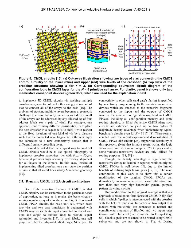
In CMOL memristive devices are integrated in the
crossbar structures which are defined on top of the
conventional CMOS substrate (Fig. 5). CMOS circuitry
provides signal restoration and gain for logic circuitry and
used to build decoders and sensing circuitry to program
memristive devices. A unique feature of CMOL circuits is
area distributed interface which enables high vertical
bandwidth, and comes with potentially very low cost and
low overhead. (Another property of such interfaces is that
it relaxes overlay alignment requirement between nano
and CMOS layers [15, 20] though this may not be
important if both CMOS and crossbar layers are
fabricated with conventional optical lithography). The
area interface is enabled by (i) the crossbar array which is
rotated by an angle α = arcsin(1/β) with respect to the
mesh of CMOS-controlled vias; and (ii) a double
decoding scheme that provides a unique access to each
crosspoint memristive device. More specifically, as Fig. 5
shows, two types of vias, one connecting to the lower
(shown with blue dots) and the other to the upper (red
dots) wire level in the crossbar, are arranged into a square
array of “basic cells” with sides 2βFCMOS. Here β > 1 is a
dimensionless number that depends on the cell size (i.e.
complexity) in the CMOS subsystem. Note that with
rotated crossbar array vias naturally subdivide the wires
into fragments of length 2(βFCMOS)2/Fnano. The factor β is
not arbitrary, but is chosen from the spectrum of possible
values β = (r2 + 1)1/2×Fnano/FCMOS, where r is an integer so
that the precise number of devices on the wire fragment is
r2 -1 ≈ β2(FCMOS/Fnano)2.
The decoding scheme in CMOL is based on two
separate address arrays (one for each level of wire in the
crossbar so that there are a total of 4N edge channels to
provide access to two different via controllers (one 'blue'
and one 'red') in each of N2 addressing cells in the CMOS
plane (Fig. 5). In contrast to standard memory arrays, in
CMOL each control and data line pair electrically
connects the peripheral input/outputs to a via instead of a
single memory element. In turn, each via is connected to a
wire fragment in the crossbar. The two perpendicular sets
of wire fragments provide unique access to any crosspoint
device even for large values of β. For example, selecting
pins δv and b4 (which are highlighted with blue and red
circles, correspondingly) provides access to the leftmost
of the two shown devices on Fig. 5a, while pins δv and c4
for the rightmost device.
The total number of crosspoint devices that can be
accessed by the N×N array of CMOS addressing cells is
~N2β2(FCMOS/Fnano)2, which may be much larger than N2,
if Fnano < FCMOS. An alternate way of looking at this fact
is that one can use complex CMOS circuitry built with a
significantly larger feature size to address regular
crossbars built on a finer lithographic scale. Furthermore,
the total number of memristive devices which can be
accessed with double decoding scheme is N4 >>
N2β2(FCMOS/Fnano)2. More specifically, the first level of
decoding selects two of 2N2 vias with 4N edge channels
using a four-label address. The second level of decoding
should, in principle, enable the selection of N4 crosspoint
devices using the 2N2 internal lines (vias) of the area
interface. This fact has been used to extend original idea
f
e
d
b
a
δ
ε
δ
γ
β
1 2 3 4 5
i ii iii iv v vi
c
α2Fnano
2(βFCMOS)2
/ Fnano
2βFCMOS
α
6
crossbar with sandwiched
memristive crosspoint devices
(top layer)
control lines for “blue” vias
control lines for “red” vias
f
e
d
c
b
a
δ
ε
δ
γ
β
α
data
lines
for
“blue”
vias
data
lines
for
“red”
vias
i ii iii iv v vi
1 2 3 4 5 6
(a) (b) (c)
CMOS stack
(bottom layer)
Figure 5. CMOL circuits [15]. (a) Cut-away illustration showing two types of vias connecting the CMOS control circuitry to the lower (blue) and upper (red) wire levels of the crossbar. (b) Top view of the crossbar structure showing α for r = 3. (c) Corresponding equivalent circuit diagram of the configuration logic in CMOS layer for the N = 5 primitive cell array. For clarity, panel b shows only two memristive crosspoint devices (green dots) which are used for the explanation in text. to implement 3D CMOL circuits via stacking multiple
crossbar arrays on top of each other using just one set of
vias to connect all of the arrays to the cells [16]. The
problem of stacking multiple layers becomes a geometric
challenge to ensure that only one crosspoint device in all
of the arrays can be addressed by any allowed set of four
address labels (or a pair of vias). For example, one
approach (out of many different possibilities) is to place
the next crossbar in a sequence is to shift it with respect
to the fixed locations of one kind of via by a distance
such that the contacted wire fragments in the new layer
are connected to a new connectivity domain that is
different from any preceding layer.
It should be noted that the simplest way to build 3D
CMOL circuits would be to use optical lithography to
implement crossbar nanowires, i.e. with Fnano = FCMOS,
because it provides high accuracy of overlay alignment
for all layers in the circuits. In this case, instead of
implementing tilted crossbar, one can rotate the position
of vias so that all metal lines satisfy Manhattan geometry
[19].
2.3. Dynamic CMOL FPGA circuit architecture
One of the attractive features of CMOL is that
CMOS circuitry can be customized to the particular needs
of application, as long as it retains the basic circuitry
serving regular array of vias shown on Fig. 5. In original
CMOL FPGA circuits, the basic unit cell, which hosts
two vias and two pass transistors, is augmented with
CMOS inverter (with its input connected to via of one
kind and output to another kind) to provide signal
restoration and inversion [17]. In such fabric, one cell
plays the role of configurable diode logic NOR gate. Its
connectivity to other cells (and gate’s fan-in) is specified
by selectively programming to the on state memristive
devices which are attached to the nanowire fragments
connected to the inputs and the outputs of CMOS
inverter. Because all configuration overhead in CMOL
FPGAs, including all configuration memory and some
routing circuitry, is lifted above the CMOS plane such
circuits are estimated to yield up to two orders of
magnitude density advantage when implementing typical
benchmark circuits even for K = 1 [17, 18]. These results,
coupled with the recent experimental demonstration of
CMOL FPGA-like circuits [28], support the feasibility of
this approach. (Note that in more recent works, the logic
fabric was built with more complex CMOS gates and in
some versions memristive devices are only utilized for
routing purposes [18, 28].)
Though the density advantage is significant, the
memristive device utilization in reported work on original
CMOL FPGAs is well below 1%, due to the limited
benefits of utilizing high fan-in gates [17, 18]. The main
contribution of this work is to show that a certain
modification of the original CMOL FPGAs can
dramatically increase memristive device utilization and
turn them into very high bandwidth general purpose
pattern matching circuits.
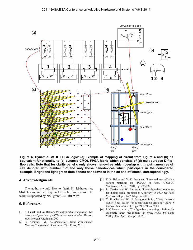
One modification to the original concept is that our
approach is based on uniform fabric of CMOS D-flip-flop
cells in which flip-flop is interconnected with the crossbar
with the help of four vias. In particular two output vias
(shown with red circle) are connected to normal and
complimentary outputs of flip-flop and two inputs ones
(shown with blue circle) are connected to D input (Fig.
6d). Clock signals are assumed to be routed using CMOS
subsystem and are not shown in Fig. 6. During
programming, CMOS flip-flop is disabled in all cells,
e.g., by having “eval” CMOS line set to low. As a result
any crosspoint memristive device (shown with green
circle on Fig. 6c) in a crossbar structure can be setup to
on or off state with the help of CMOS pass transistors and
CMOS data and select lines, i.e. utilizing double decoding
scheme of CMOL which was described above.
The second modification is dynamic style of logic
similar to the pattern matching operation performed by
TCAM circuitry considered above (Fig. 2). Such
modification is necessary since static diode logic
proposed in original CMOL FPGAs is not scalable for
larger fan-ins. In particular, after the programming stage,
logic operations are implemented with dynamic diode
logic formed by ON-state memristive devices and CMOS
pass transistors, while signal restoration, inversion, and
latching is performed by CMOS D-flip-flop (Fig. 6).
More specifically, the logical summation (i.e. Boolean
“OR” operation) is performed in dynamic fashion in two
stages during the clock period. During the first shorter
stage the outputs of flip-flop in all cells are disconnected
from corresponding crossbar wire using CMOS “eval”
line. At the same time crossbar wire connected to the
inputs and the outputs of flip-flop are precharged to high
voltage using “select/pre” and “data/pre” CMOS lines.
During the second stage, the “eval” signal is set to “high”
voltage. This results in logical summation of the values
from the cells connected to the particular crossbar wire
with memristive devices turned to the ON state. At the
rising clock edge, the value latched at the flip flop so that
it can be used in unchanged or complimented form in the
next clock cycle. Note that, though the operation
performed on the crossbar wire is equivalent to OR
Boolean operation, Boolean AND could also be
performed in one cycle utilizing De Morgan’s law due to
the presence of complimentary outputs Q.
3. Discussion and summary
Let us now estimate performance of dynamic CMOL
FPGAs. From the discussion so far it is clear that one flip
flop cell can perform pattern matching in TCAM fashion
in just one clock cycle (Fig. 6). The maximum size of a
pattern is determined by the number of memristive
devices attached to two input nanowires of flip-flop cell,
i.e. quasi vertical ones on Fig. 6c, which is equal to 2(r2 –
1) for one crossbar layer (see discussion of that in the
previous section) and 2K(r2 – 1) for CMOL circuits with
K layers.
The universal flip-flop cells could be also configured
to perform Boolean logic operations, e.g., to perform
logical operation with the results of pattern matching
operation and/or to stream data, e.g. by forming very deep
pipelines. For example, given array of flip-flop cells one
can configure every second row of cells to stream data,
from left to right on Fig. 6, and have remaining cells to
perform pattern matching. With such mapping the
maximum pattern matching capacity per one flip-flop cell
is Nbits = 1/2 × 1/2 × 2K(r2 – 1). Here the first factor of 1/2
reflects the fact that only half of flip-flop cells is involved
in pattern matching operation (the other half is used for
streaming), and the second one that only half of the
memristive devices can be used for pattern matching in
the simplest case (i.e. only memristive devices
programmed to connect to flip-flop cells which streams
data). With such mapping the effective density of patterns
stored and processed is just 1/4 of the maximum passive
crossbar memory capacity.
We can also estimate the minimum clock cycle by
assuming that all power is dynamic, because the static
leakage could be neglected for the memristive devices
with high on-off ratio. The maximum clock frequency f
can be found from the equation CwireV2 fmax/2 = pmax Acell,
where V is a voltage swing, Cwire ≈ 4 × 2Fnano× Kr2 × Cseg
is a total capacitance charged per cycle for one cell (i.e. of
4 nanowire segments with Cseg capacitance per unit
length), pmax = 200 W/cm2 is a typical manageable power
consumption density [10], and Acell = 2 × (2βFCMOS)2 is a
flip-flop cell area. For example, assuming rather
conservative values V = 1V, β = 10, K = 1 and using
data from Ref. [17] for crossbar wire capacitance, fmax ≈
pmax Fnano / (K Cseg V2) ≈ 100 MHz for Fnano = 3 nm and
FCMOS = 45 nm, and fmax ≈ 1 GHz for Fnano = 45 nm and
FCMOS = 130 nm. The pattern matching throughputs per
unit area, defined as Nbits fmax/Acell, corresponding to these
two cases are 1019 and 1018 bits/s/cm2, respectively, which
is much higher than any reported state-of-the art concepts.
Also note that the proposed circuits could potentially
offer much higher pattern capacity without any
performance penalty. Because the number of storage
elements in existing hardware-based pattern matchers is
limited by the 2D chip area, they must be dynamically
reconfigured to accommodate additional patterns that are
beyond their storage capabilities. Dynamic
reconfiguration is a relatively slow process, and if pattern
matcher could not fit all the patterns the throughput for a
fixed area will be considerably smaller than the ideal
value. On the other hand, the bit capacity of the dynamic
CMOL FPGA can be seamlessly increased by integrating
more crossbar layers using the multilayer CMOL idea
[24]. Thus, our architecture can support more patterns
without any degradation in throughput.
In conclusion, we believe that the proposed circuits
are very promising for pattern matching applications. It is
worth mentioning that the current main challenge towards
building such circuits is yield of today’s memristive
devices, even considering high intrinsic defect tolerance
of CMOL FPGAs [17]. However, large scale industrial
efforts on passive crossbar memories give hope that this
issue might soon be resolved.
3
(a)Mpre
pre
ON OFF OFF ON OFF OFF ON OFF
eval
data/pre
select/pre
eval
DQQ’
select/pre
select/pre
select/predata/pre
4
12
5
1 2 3 4
5
DQ Q’
DQ Q’
DQ Q’
DQ Q’
DQ
Q’
DQQ’
12 4
(c)
(b)
(d)
CMOS flip-flop cell
crossbar wire
nanodevice
Figure 6. Dynamic CMOL FPGA logic: (a) Example of mapping of circuit from Figure 4 and (b) its equivalent functionality to (c) dynamic CMOL FPGA fabric which consists of (d) multipurpose D-flip-flop cells. Note that for clarity panel c only shows nanowires which overlap with input nanowires of cell denoted with number “5” and only those nanodevices which participate in the considered example. Bright and light green dots denote nanodevices in the on and off states, correspondingly.
4. Acknowledgments
The authors would like to thank K. Likharev, A.
Mishchenko, and R. Brayton for useful discussions. The
work is supported by NSF grant CCF-1017579.
5. References
[1] S. Hauck and A. DeHon, Reconfigurable computing: The
theory and practice of FPGA-based computation. Boston,
MA: Morgan Kaufmann, 2008.
[2] B. Schmidt, Ed., Bioinformatics: High Performance
Parallel Computer Architectures. CRC Press, 2010.
[3] Z. K. Baker and V. K. Prasanna, "Time and area efficient
pattern matching on FPGAs," in Proc. FPGA'04,
Monterey, CA, Feb. 2004, pp. 223-232.
[4] R. Tessier and W. Burleson, "Reconfigurable computing
for digital signal processing: A survey," J VLSI Sig Proc
Syst, vol. 28, pp. 7-27, May-Jun 2001.
[5] Y. H. Cho and W. H. Mangione-Smith, "Deep network
packet filter design for reconfigurable devices," ACM T
Embed Comput S, vol. 7, pp. 21:1-21:26, 2008.
[6] J. Villasenor, et al., "Configurable computing solutions for
automatic target recognition," in Proc. FCCM'96, Napa
Valley, CA, Apr. 1996, pp. 70-79.
[7] I. Kuon and J. Rose, "Measuring the gap between FPGAs
and ASICs," IEEE T Comput Aid D, vol. 26, pp. 203-215,
Feb 2007.
[8] I. Sourdis and D. Pnevmatikatos, "Pre-decoded CAMs for
efficient and high-speed NIDS pattern matching," in Proc.
FCCM'04, Napa, CA, Apr. 2004, pp. 258-267.
[9] K. Pagiamtzis and A. Sheikholeslami, "Content-
addressable memory (CAM) circuits and architectures: A
tutorial and survey," IEEE J Solid-St Circ, vol. 41, pp. 712-
727, Mar 2006.
[10] International Technology Roadmap for Semiconductors,
2007 Edition, Available online at http://www.itrs.net.
[11] W. Xu, et al., "Design of spin-torque transfer
magnetoresistive RAM and CAM/TCAM with high
sensing and search speed," IEEE T VLSI Syst, vol. 18, pp.
66-74, Jan 2010.
[12] T. Hanyu, et al., "Non-volatile one-transistor-cell multiple-
valued CAM with a digit-parallel-access scheme and its
applications," Comput Electr Eng, vol. 23, pp. 407-414,
Nov 1997.
[13] K. Eshraghian, et al., "Memristor MOS content addressable
memory (MCAM): Hybrid Architecture for Future High
Performance Search Engines " IEEE T Nanotechnogy, in
print, 2011.
[14] S. Matsunaga, et al., "Standby-power-free compact ternary
content-addressable memory cell chip using magnetic
tunnel junction devices," Appl Phys Express, vol. 2, pp.
023004, Feb 2009.
[15] K. K. Likharev and D. B. Strukov, "CMOL: Devices,
circuits, and architectures," Lecture Notes in Physics, vol.
680, pp. 447-477, 2006.
[16] D. B. Strukov and R. S. Williams, "Four-dimensional
address topology for circuits with stacked multilayer
crossbar arrays," P Natl Acad Sci USA, vol. 106, pp.
20155-20158, Dec 1 2009.
[17] D. B. Strukov and K. K. Likharev, "CMOL FPGA: A
reconfigurable architecture for hybrid digital circuits with
two-terminal nanodevices," Nanotechnology, vol. 16, pp.
888-900, Jun 2005.
[18] D. B. Strukov and K. K. Likharev, "A reconfigurable
architecture for hybrid CMOS/nanodevice circuits," in
Proc. FPGA'06, Monterey, CA, Feb. 2006, pp. 131-140.
[19] D. Strukov and A. Mishchenko, "Monolithically stackable
hybrid FPGA," in Proc. DATE'10, Dresden, Germany,
Mar. 2010, pp. 661-666.
[20] K. K. Likharev, "Hybrid CMOS/Nanoelectronic Circuits:
Opportunities and Challenges," J Nanoelectron Optoe, vol.
3, pp. 203-230, Dec 2008.
[21] R. Waser, et al., "Redox-based resistive switching
memories - nanoionic mechanisms, prospects, and
challenges," Adv Mater, vol. 21, pp. 2632-2663, Jul 13
2009.
[22] Y. C. Pershin and M. D. Ventra, "Memory effects in
complex materials and nanoscale systems," Advances in
Physics, vol. 60, pp. 145-227, 2011.
[23] J. Borghetti, et al., "Electrical transport and thermometry
of electroformed titanium dioxide memristive switches," J
Appl Phys, vol. 106, art. 124504 , Dec 15 2009.
[24] J. J. Yang, et al., "Memristive switching mechanism for
metal/oxide/metal nanodevices," Nat Nanotechnol, vol. 3,
pp. 429-433, Jul 2008.
[25] R. Meyer, et al., "Oxide dual-layer memory element for
scalable non-volatile cross-point memory technology," in
Proc. Nonvolatile Memory Technology Symposium,
Monterey, CA, Nov. 2008, pp. 54-58.
[26] I. G. Baek, et al., "Multi-layer cross-point binary oxide
resistve memory (OxRRAM) for post-NAND storage
application," in Proc. Electron Device Meeting,
Washington, DC, Dec. 2005, pp. 750-753.
[27] L. Tan and T. Sherwood, "Architectures for bit-split string
scanning in intrusion detection," IEEE Micro, vol. 26, pp.
110-117, Jan-Feb 2006.
[28] Q. F. Xia, et al., "Memristor-CMOS Hybrid Integrated
Circuits for Reconfigurable Logic," Nano Lett, vol. 9, pp.
3640-3645, Oct 2009.