Embed Size (px)
Citation preview
HSSR-7110, HSSR-7111, HSSR-7112,
HSSR-711E, 5962-9314001, 5962-93140021
90V/1.0Ω, Hermetically Sealed, Power MOSFET Optocoupler
Data Sheet
DescriptionThe Broadcom® HSSR-7110, HSSR-7111, HSSR-7112, HSSR-711E and SMD 5962-9314001, 5962-9314002 are single-channel power MOSFET optocouplers, constructed in eight-pin, hermetic, dual-in-line, ceramic packages. The devices operate exactly like a solid-state relay.
The products are capable of operation and storage over the full military temperature range and can be purchased as a commercial product (HSSR-7110), with full MIL-PRF-38534 Class H testing (HSSR-7111 and HSSR- 7112), with MIL-PRF-38534 Class E testing (Class K with exceptions) (HSSR-711E) or from the DLA Standard Microcircuit Drawing (SMD) 5962-93140. Details of the Class E program exceptions are listed here:
1. Nondestructive Bond Pull, Test method 2023 of MIL-STD-883 in device screening is not required.
2. Particle Impact Noise Detection (PIND), Test method 2020 of MIL-STD-883 in device screening and group C testing is not required.
3. Die Shear Strength, Test method 2019 of MIL-STD-883 in group B testing is not required.
4. Internal Water Vapor Content, Test method 1018 of MIL-STD-883 in group C testing is not required.
5. Scanning Electron Microscope (SEM) inspections, Test method 2018 of MIL-STD-883 in element evaluation is not required.
1. See Selection Guide – Lead Configuration Options for available extensions.
Features Dual marked with device part number and DLA Standard
Microcircuit Drawing (SMD) ac/dc signal and power switching Compact solid-state bidirectional switch Manufactured and tested on a MIL-PRF-38534 certified line QML-38534, Class H and Class E Hermetically sealed 8-pin, dual-in-line package Small size and weight Performance guaranteed over –55°C to +125°C Connection A 0.8A, 1.0Ω Connection B 1.6A, 0.25Ω 1500 Vdc withstand test voltage High transient immunity 5 Amp output surge current
Applications Military and space High reliability systems Standard 28 Vdc and 48 Vdc load driver Standard 24 Vac load driver Aircraft controls ac/dc electromechanical and solid-state relay replacement I/O modules Harsh industrial environments
CAUTION It is advised that normal static precautions be taken in handling and assembly of this component to prevent damage and/or degradation that may be induced by ESD.
Broadcom- 1 -
HSSR-7110, HSSR-7111, HSSR-7112, HSSR-711E, 5962-9314001, 5962-9314002Data Sheet
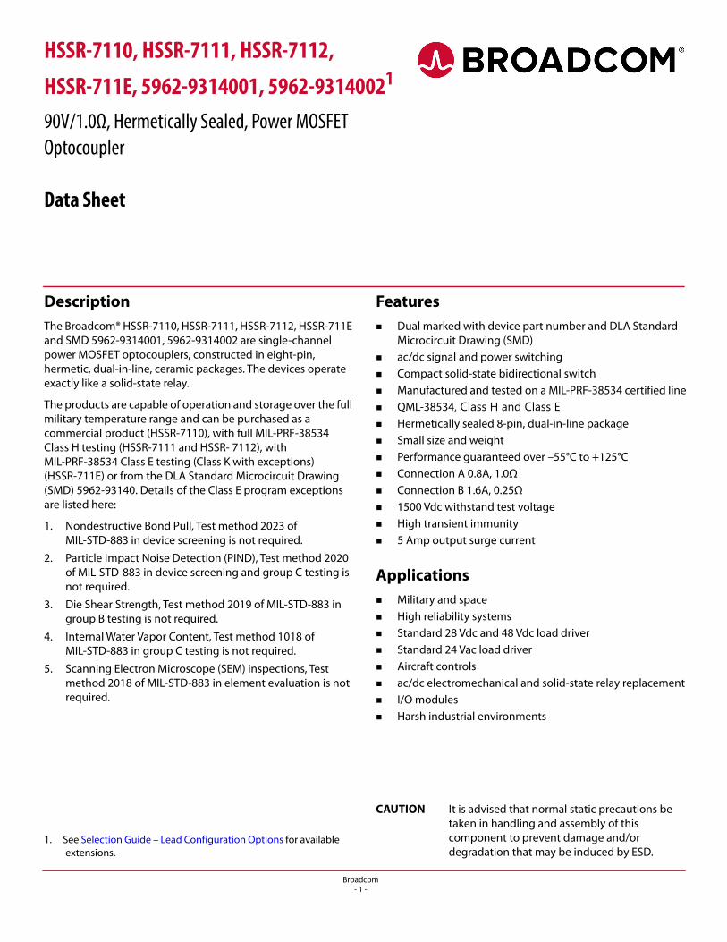
Functional Diagrams
Functional Diagrams
All devices are manufactured and tested on a MIL-PRF-38534 certified line, and Class H and Class E devices are included in the DLA Qualified Manufacturers List, QML-38534 for Hybrid Microcircuits. Each device contains an AlGaAs light-emitting diode optically coupled to a photovoltaic diode stack, which drives two discrete power MOSFETs. The device operates as a solid-state replacement for single-pole, normally open (1 Form A) relay used for general-purpose switching of signals and loads in high reliability applications.
The devices feature logic level input control and very low output on-resistance, making them suitable for both ac and dc loads. Connection A, as shown in the Functional Diagrams, allows the device to switch either ac or dc loads. Connection B, with the polarity and pin configuration as shown, allows the device to switch dc loads only. The advantage of Connection B is that the on-resistance is significantly reduced, and the output current capability increases by a factor of two.
The devices are convenient replacements for mechanical and solid-state relays where high component reliability with standard footprint lead configuration is desirable. Devices may be purchased with a variety of lead bend and plating options. See Selection Guide – Lead Configuration Options table for details. Standard microcircuit drawing (SMD) parts are available for each package and lead style.
The HSSR-7110, HSSR-7111, HSSR-7112, HSSR-711E, and SMD 5962-9314001, 5962-9314002 are designed to switch loads on 28 Vdc power systems. They meet 80V surge and ±600V spike requirements.
CAUTION Maximum Switching Frequency – Care should be taken during repetitive switching of loads so as not to exceed the maximum output current, maximum output power dissipation, maximum case temperature, and maximum junction temperature.
CONNECTION A AC/DC CONNECTION
2
3
4
1
6
7
5
8
NC
NC
+
-
+
-
CONNECTION BDC CONNECTION
IF
V F
IO
V O
2
3
4
1
6
7
5
8
NC
NC
+
-
+
-IF
V F
IO
V O
TRUTH TABLE
INPUT OUTPUT
H CLOSED
L OPEN
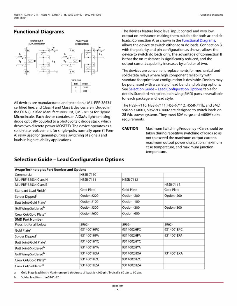
Selection Guide – Lead Configuration Options
Avago Technologies Part Number and OptionsCommercial HSSR-7110MIL-PRF-38534 Class H HSSR-7111 HSSR-7112MIL-PRF-38534 Class E HSSR-711E
Standard Lead Finisha
a. Gold Plate lead finish: Maximum gold thickness of leads is <100 μin. Typical is 60 μin to 90 μin.
Gold Plate Gold Plate Gold Plate
Solder Dippedb
b. Solder lead finish: Sn63/Pb37.
Option #200 Option -200 Option -200
Butt Joint/Gold Platea Option #100 Option -100
Gull Wing/Solderedb Option #300 Option -300 Option -300
Crew Cut/Gold Platea Option #600 Option -600
SMD Part NumberPrescript for all below 5962- 5962- 5962-
Gold Platea 9314001HPC 9314002HPC 9314001EPC
Solder Dippedb 9314001HPA 9314002HPA 9314001EPA
Butt Joint/Gold Platea 9314001HYC 9314002HYC
Butt Joint/Solderedb 9314001HYA 9314002HYA
Gull Wing/Solderedb 9314001HXA 9314002HXA 9314001EXA
Crew Cut/Gold Platea 9314001HZC 9314002HZC
Crew Cut/Solderedb 9314001HZA 9314002HZA
Broadcom- 2 -
HSSR-7110, HSSR-7111, HSSR-7112, HSSR-711E, 5962-9314001, 5962-9314002Data Sheet
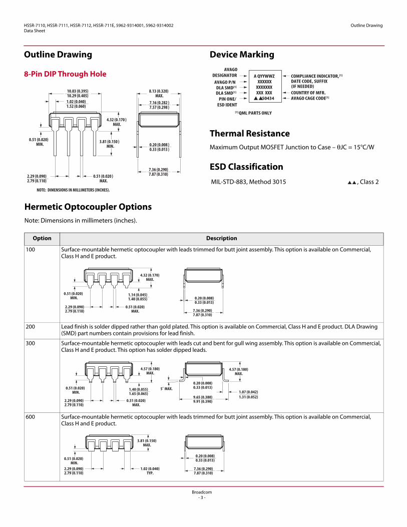
Outline Drawing
Outline Drawing
8-Pin DIP Through Hole
Device Marking
Thermal ResistanceMaximum Output MOSFET Junction to Case – θJC = 15°C/W
ESD Classification
3.81 (0.150 )MIN.
4.32 (0.170 )MAX.
10.03 (0.395)10.29 (0.405)
0.51 (0.020 )MAX.
2.29 (0.090)2.79 (0.110)
0.51 (0.020)MIN.
1.02 (0.040)1.52 (0.060)
8.13 (0.320)MAX.
7.36 (0.290)7.87 (0.310)
0.20 (0.008 )0.33 (0.013 )
7.16 (0.282 )7.57 (0.298 )
NOTE: DIMENSIONS IN MILLIMETERS (INCHES).
MIL-STD-883, Method 3015 , Class 2
COMPLIANCE INDICATOR,[1]
DATE CODE, SUFFIXA QYYWWZ
XXXXXXXXXXXXXXXX XXX 50434
COUNTRY OF MFR.AVAGO CAGE CODE[1]
AVAGODESIGNATOR
DLA SMD[1]
PIN ONE/ESD IDENT
AVAGO P/NDLA SMD[1]
[1] QML PARTS ONLY
(IF NEEDED)
Hermetic Optocoupler OptionsNote: Dimensions in millimeters (inches).
Option Description
100 Surface-mountable hermetic optocoupler with leads trimmed for butt joint assembly. This option is available on Commercial, Class H and E product.
200 Lead finish is solder dipped rather than gold plated. This option is available on Commercial, Class H and E product. DLA Drawing (SMD) part numbers contain provisions for lead finish.
300 Surface-mountable hermetic optocoupler with leads cut and bent for gull wing assembly. This option is available on Commercial, Class H and E product. This option has solder dipped leads.
600 Surface-mountable hermetic optocoupler with leads trimmed for butt joint assembly. This option is available on Commercial, Class H and E product.
1.14 (0.045)1.40 (0.055)
4.32 (0.170)MAX.
0.51 (0.020)MAX.
2.29 (0.090)2.79 (0.110)
0.51 (0.020)MIN.
7.36 (0.290)7.87 (0.310)
0.20 (0.008)0.33 (0.013)
0.51 (0.020)MIN.
4.57 (0.180)MAX.
0.51 (0.020)MAX.
2.29 (0.090)2.79 (0.110)
1.40 (0.055)1.65 (0.065)
9.65 (0.380)9.91 (0.390)
5˚ MAX.
4.57 (0.180)MAX.
0.20 (0.008)0.33 (0.013)
1.07 (0.042)1.31 (0.052)
3.81 (0.150)MAX.
1.02 (0.040)TYP.
2.29 (0.090)2.79 (0.110)
0.51 (0.020)MIN.
7.36 (0.290)7.87 (0.310)
0.20 (0.008)0.33 (0.013)
Broadcom- 3 -
HSSR-7110, HSSR-7111, HSSR-7112, HSSR-711E, 5962-9314001, 5962-9314002Data Sheet
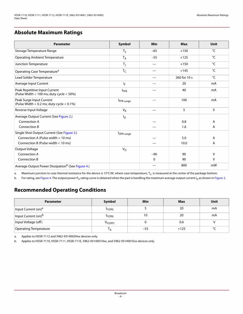
Absolute Maximum Ratings
Absolute Maximum Ratings
Recommended Operating Conditions
Parameter Symbol Min Max Unit
Storage Temperature Range TS –65 +150 °C
Operating Ambient Temperature TA –55 +125 °C
Junction Temperature TJ — +150 °C
Operating Case Temperaturea
a. Maximum junction to case thermal resistance for the device is 15°C/W, where case temperature, TC, is measured at the center of the package bottom.
TC — +145 °C
Lead Solder Temperature — 260 for 10 s °C
Average Input Current IF — 20 mA
Peak Repetitive Input Current(Pulse Width < 100 ms; duty cycle < 50%)
IFPK — 40 mA
Peak Surge Input Current (Pulse Width < 0.2 ms; duty cycle < 0.1%)
IFPK surge — 100 mA
Reverse Input Voltage VR — 5 V
Average Output Current (See Figure 2.) Connection A Connection B
IO——
0.81.6
AA
Single Shot Output Current (See Figure 3.) Connection A (Pulse width < 10 ms) Connection B (Pulse width < 10 ms)
IOPK surge——
5.010.0
AA
Output Voltage Connection A Connection B
VO–90
09090
VV
Average Output Power Dissipationb (See Figure 4.)
b. For rating, see Figure 4. The output power PO rating curve is obtained when the part is handling the maximum average output current IO as shown in Figure 2.
— 800 mW
Parameter Symbol Min Max Unit
Input Current (on)a
a. Applies to HSSR-7112 and 5962-9314002Hxx devices only.
IF(ON) 5 20 mA
Input Current (on)b
b. Applies to HSSR-7110, HSSR-7111, HSSR-711E, 5962-9314001Hxx, and 5962-9314001Exx devices only.
IF(ON) 10 20 mA
Input Voltage (off ) VF(OFF) 0 0.6 V
Operating Temperature TA –55 +125 °C
Broadcom- 4 -
HSSR-7110, HSSR-7111, HSSR-7112, HSSR-711E, 5962-9314001, 5962-9314002Data Sheet
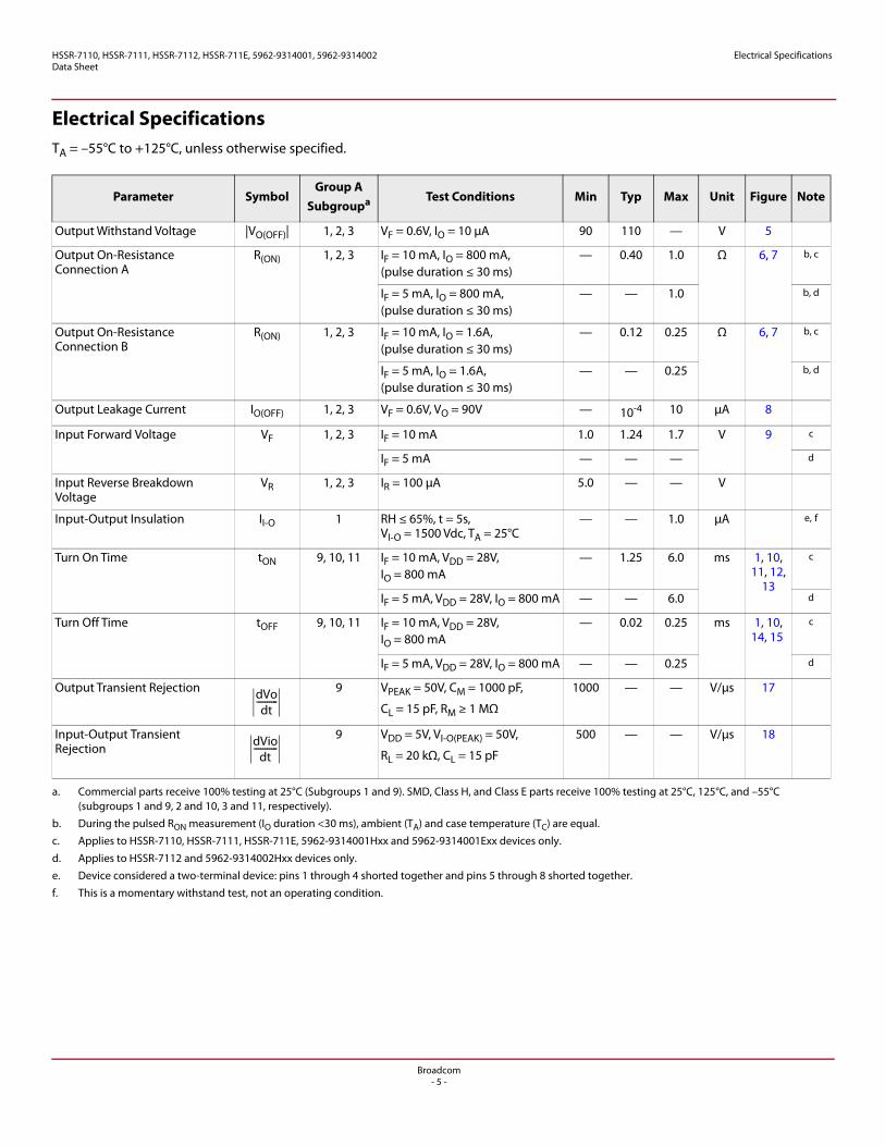
Electrical Specifications
Electrical SpecificationsTA = –55°C to +125°C, unless otherwise specified.
Parameter SymbolGroup A
Subgroupa
a. Commercial parts receive 100% testing at 25°C (Subgroups 1 and 9). SMD, Class H, and Class E parts receive 100% testing at 25°C, 125°C, and –55°C (subgroups 1 and 9, 2 and 10, 3 and 11, respectively).
Test Conditions Min Typ Max Unit Figure Note
Output Withstand Voltage |VO(OFF)| 1, 2, 3 VF = 0.6V, IO = 10 μA 90 110 — V 5
Output On-Resistance Connection A
R(ON) 1, 2, 3 IF = 10 mA, IO = 800 mA,(pulse duration ≤ 30 ms)
— 0.40 1.0 Ω 6, 7 b, c
b. During the pulsed RON measurement (IO duration <30 ms), ambient (TA) and case temperature (TC) are equal.
c. Applies to HSSR-7110, HSSR-7111, HSSR-711E, 5962-9314001Hxx and 5962-9314001Exx devices only.
IF = 5 mA, IO = 800 mA, (pulse duration ≤ 30 ms)
— — 1.0 b, d
d. Applies to HSSR-7112 and 5962-9314002Hxx devices only.
Output On-Resistance Connection B
R(ON) 1, 2, 3 IF = 10 mA, IO = 1.6A, (pulse duration ≤ 30 ms)
— 0.12 0.25 Ω 6, 7 b, c
IF = 5 mA, IO = 1.6A, (pulse duration ≤ 30 ms)
— — 0.25 b, d
Output Leakage Current IO(OFF) 1, 2, 3 VF = 0.6V, VO = 90V — 10-4 10 μA 8
Input Forward Voltage VF 1, 2, 3 IF = 10 mA 1.0 1.24 1.7 V 9 c
IF = 5 mA — — — d
Input Reverse Breakdown Voltage
VR 1, 2, 3 IR = 100 μA 5.0 — — V
Input-Output Insulation II-O 1 RH ≤ 65%, t = 5s, VI-O = 1500 Vdc, TA = 25°C
— — 1.0 μA e, f
e. Device considered a two-terminal device: pins 1 through 4 shorted together and pins 5 through 8 shorted together.
f. This is a momentary withstand test, not an operating condition.
Turn On Time tON 9, 10, 11 IF = 10 mA, VDD = 28V, IO = 800 mA
— 1.25 6.0 ms 1, 10, 11, 12,
13
c
IF = 5 mA, VDD = 28V, IO = 800 mA — — 6.0 d
Turn Off Time tOFF 9, 10, 11 IF = 10 mA, VDD = 28V, IO = 800 mA
— 0.02 0.25 ms 1, 10, 14, 15
c
IF = 5 mA, VDD = 28V, IO = 800 mA — — 0.25 d
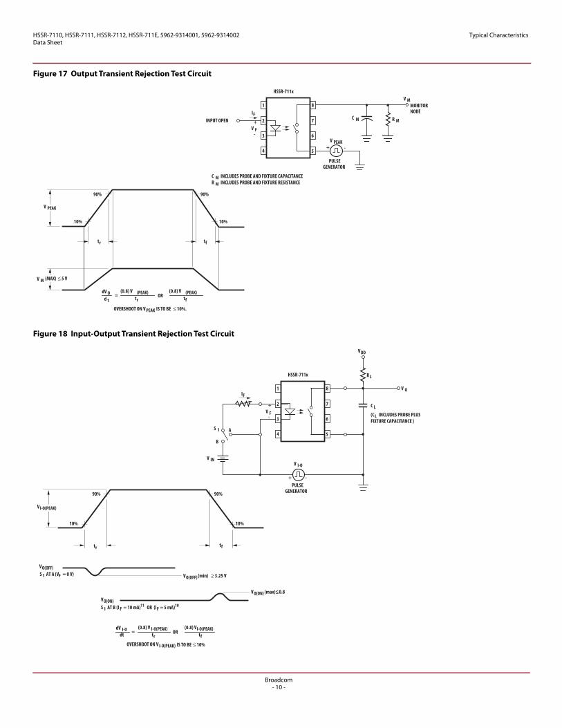
Output Transient Rejection 9 VPEAK = 50V, CM = 1000 pF,
CL = 15 pF, RM ≥ 1 MΩ
1000 — — V/μs 17
Input-Output Transient Rejection
9 VDD = 5V, VI-O(PEAK) = 50V,
RL = 20 kΩ, CL = 15 pF
500 — — V/μs 18
dVodt----------
dViodt-----------
Broadcom- 5 -
HSSR-7110, HSSR-7111, HSSR-7112, HSSR-711E, 5962-9314001, 5962-9314002Data Sheet
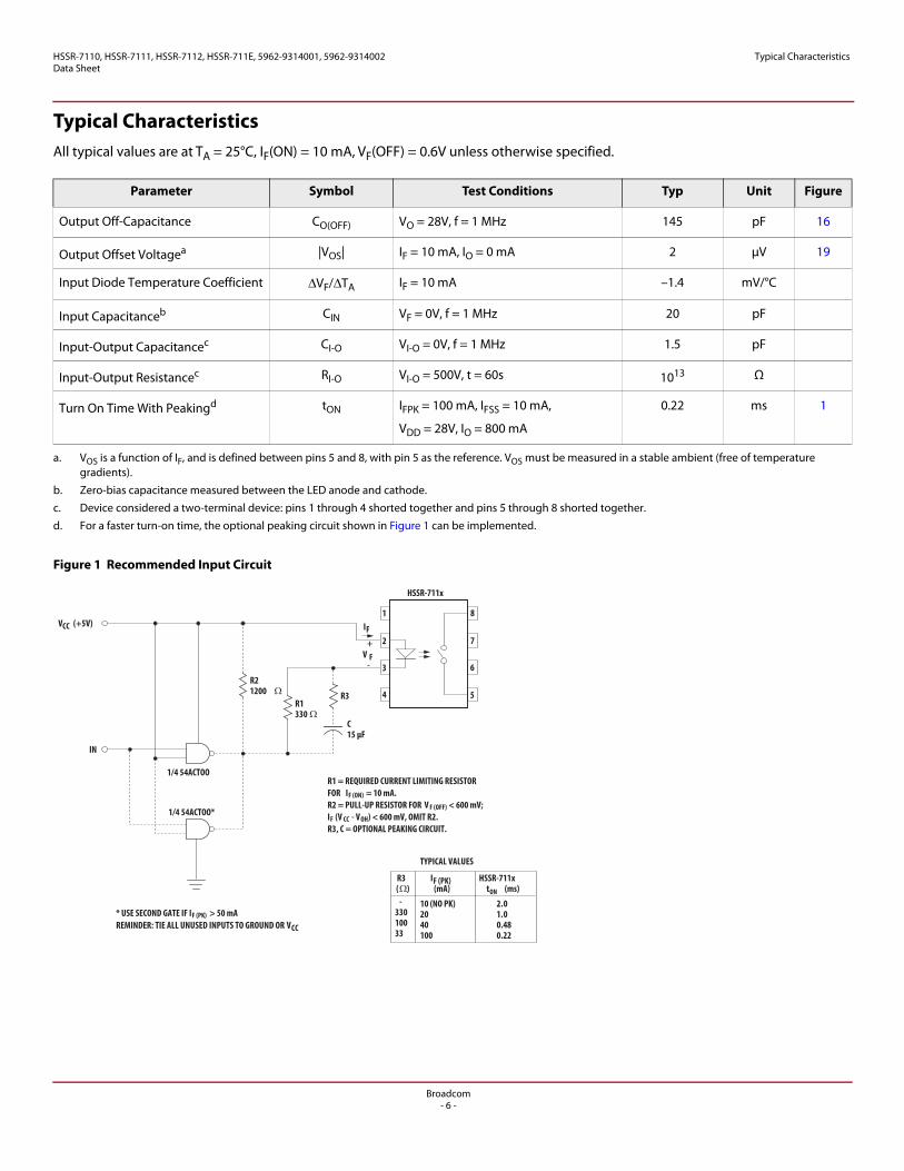
Typical Characteristics
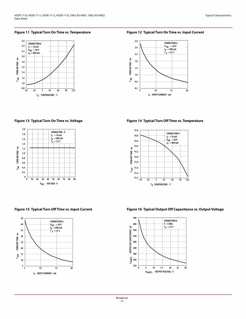
Typical CharacteristicsAll typical values are at TA = 25°C, IF(ON) = 10 mA, VF(OFF) = 0.6V unless otherwise specified.
Figure 1 Recommended Input Circuit
Parameter Symbol Test Conditions Typ Unit Figure
Output Off-Capacitance CO(OFF) VO = 28V, f = 1 MHz 145 pF 16
Output Offset Voltagea
a. VOS is a function of IF, and is defined between pins 5 and 8, with pin 5 as the reference. VOS must be measured in a stable ambient (free of temperature gradients).
|VOS| IF = 10 mA, IO = 0 mA 2 μV 19
Input Diode Temperature Coefficient ΔVF/ΔTA IF = 10 mA –1.4 mV/°C
Input Capacitanceb
b. Zero-bias capacitance measured between the LED anode and cathode.
CIN VF = 0V, f = 1 MHz 20 pF
Input-Output Capacitancec
c. Device considered a two-terminal device: pins 1 through 4 shorted together and pins 5 through 8 shorted together.
CI-O VI-O = 0V, f = 1 MHz 1.5 pF
Input-Output Resistancec RI-O VI-O = 500V, t = 60s 1013 Ω
Turn On Time With Peakingd
d. For a faster turn-on time, the optional peaking circuit shown in Figure 1 can be implemented.
tON IFPK = 100 mA, IFSS = 10 mA,
VDD = 28V, IO = 800 mA
0.22 ms 1
R1 = REQUIRED CURRENT LIMITING RESISTOR FOR IF (ON) = 10 mA.R2 = PULL-UP RESISTOR FOR V F (OFF) < 600 mV;IF (V CC - VOH ) < 600 mV, OMIT R2.R3, C = OPTIONAL PEAKING CIRCUIT.
TYPICAL VALUES
R3( )
IF (PK)(mA)
HSSR-711x tON (ms)
-33010033
10 (NO PK)2040100
2.01.00.480.22
* USE SECOND GATE IF IF (PK) > 50 mAREMINDER: TIE ALL UNUSED INPUTS TO GROUND OR VCC
IN
1/4 54ACTOO*
1/4 54ACTOO
VCC (+5V)
R21200
R1330
R3
C15 μF
HSSR-711x
2
3
4
1
6
7
5
8
-
IF
V F
+
Broadcom- 6 -
HSSR-7110, HSSR-7111, HSSR-7112, HSSR-711E, 5962-9314001, 5962-9314002Data Sheet
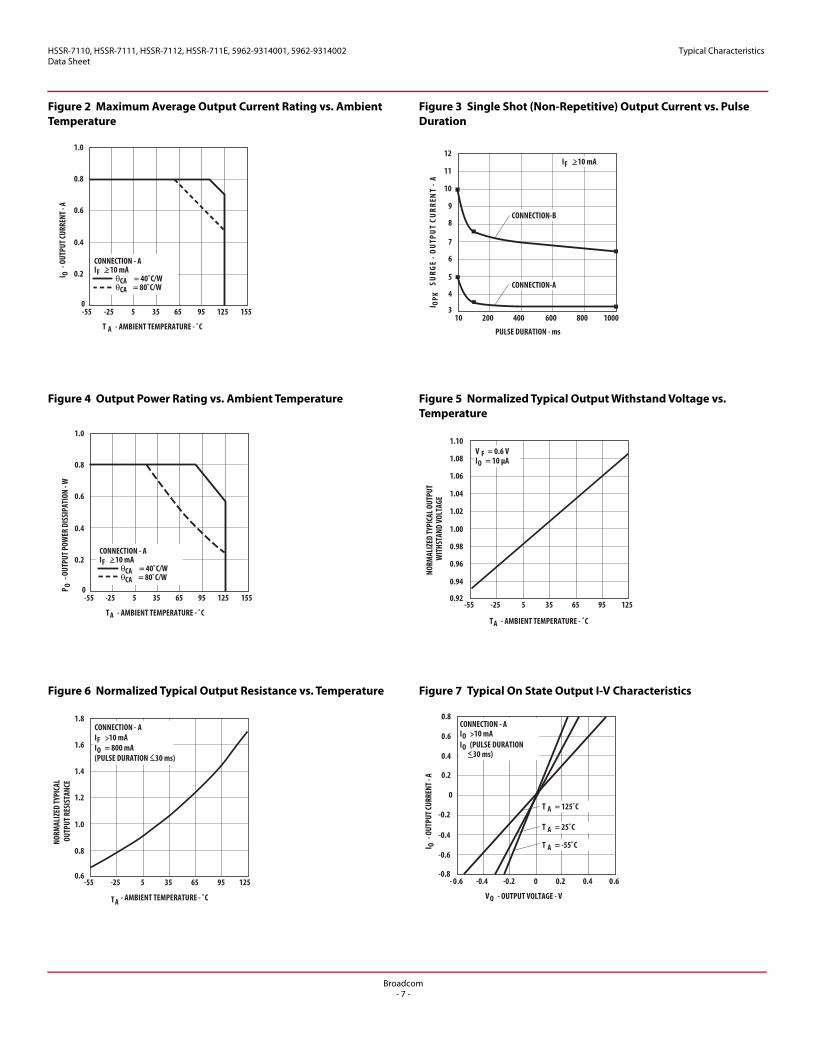
Typical Characteristics
Figure 2 Maximum Average Output Current Rating vs. Ambient Temperature
Figure 3 Single Shot (Non-Repetitive) Output Current vs. Pulse Duration
0-55
T A - AMBIENT TEMPERATURE - ˚C
1.0
0.4
15512595655-25
0.6
0.8
0.2
35
I O - O
UTPU
T CUR
RENT
- A
CONNECTION - AIF 10 mA
CA = 40˚C/WCA = 80˚C/W
I KPO
- TNERR
UC TUPT
UO - EGRUS
A
31000
PULSE DURATION - ms
8
5
400200
6
7
4
9
10
11
12
600 800
IF 10 mA
CONNECTION-A
CONNECTION-B
10
Figure 4 Output Power Rating vs. Ambient Temperature Figure 5 Normalized Typical Output Withstand Voltage vs. Temperature
0-55
TA - AMBIENT TEMPERATURE - ˚C
1.0
0.4
15512595655-25
0.6
0.8
0.2
35
P O - O
UTPU
T POW
ER D
ISSI
PATI
ON - W
CONNECTION - AIF 10 mA
CA = 40˚C/WCA = 80˚C/W
V F = 0.6 VIO = 10 μA
-55
TA - AMBIENT TEMPERATURE - ˚C
12595655-250.92
35
NORM
ALIZ
ED TY
PICA
L OUT
PUT
WIT
HSTA
ND V
OLTA
GE
0.94
0.96
0.98
1.00
1.02
1.04
1.06
1.08
1.10
Figure 6 Normalized Typical Output Resistance vs. Temperature Figure 7 Typical On State Output I-V Characteristics
NORM
ALIZ
ED TY
PICA
L OU
TPUT
RES
ISTA
NCE
-55
TA - AMBIENT TEMPERATURE - ˚C
12595655-250.6
35
0.8
1.0
1.2
1.4
1.6
1.8CONNECTION - AIF 10 mAIO = 800 mA(PULSE DURATION 30 ms)
VO - OUTPUT VOLTAGE - V
I O - O
UTPU
T CUR
RENT
- A
6.06.0- 0.40.2-0.2-0.4
-0.4
0
-0.2
0
0.2
0.4
0.6
0.8
-0.8
-0.6
CONNECTION - AIO 10 mAIO (PULSE DURATION 30 ms)
T A = 25˚C
T A = 125˚C
T A = -55˚C
Broadcom- 7 -
HSSR-7110, HSSR-7111, HSSR-7112, HSSR-711E, 5962-9314001, 5962-9314002Data Sheet
Typical Characteristics
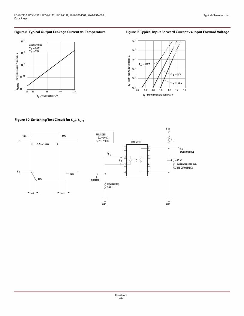
Figure 8 Typical Output Leakage Current vs. Temperature Figure 9 Typical Input Forward Current vs. Input Forward Voltage
-1110
-710
-810
-910
-1010
I O (O
FF)
- OUT
PUT L
EAKA
GE CU
RREN
T - A
TA - TEMPERATURE - ˚C
125956520 35
CONNECTION AV F = 0.6 VV O = 90 V
T A = 25˚C
T A = 125˚C
T A = -55˚C
VF - INPUT FORWARD VOLTAGE - V
6.16.0 1.41.20.80.4 1.0
-110
-210
-410
-310
-510
-610
I F - I
NPUT
FORW
ARD
CURR
ENT -
A
Figure 10 Switching Test Circuit for tON, tOFF
50%
10%
50%
90%
tON tOFF
P.W. = 15 ms
V O
IF
PULSE GEN.Z O = 50
tf = t r = 5 ns R L
GND
(C L INCLUDES PROBE ANDFIXTURE CAPACITANCE)
V DD
C L = 25 pF
IFMONITOR
R (MONITOR)200
GND
MONITOR NODEV O
HSSR-711x
2
3
4
1
6
7
5
8
-
IF
V F
+
Broadcom- 8 -
HSSR-7110, HSSR-7111, HSSR-7112, HSSR-711E, 5962-9314001, 5962-9314002Data Sheet
Typical Characteristics
Figure 11 Typical Turn On Time vs. Temperature Figure 12 Typical Turn On Time vs. Input Current
TA - TEMPERATURE - ˚C
0.8
2.2
2.0
1.8
1.6
1.4
1.2
1.0
2.4
2.6
TON
- TUR
N ON
TIM
E - m
s
52155- 95655-25 35
CONNECTION AIF = 10 mAVDD = 28 VIO = 800 mA
IF - INPUT CURRENT - mA
10 15 2050.2
2.2
1.8
1.4
1.0
0.6
2.6
3.0
TON
- TUR
N ON
TIM
E - m
s
CONNECTION AV DD = 28 VIO = 800 mAT A = 25˚C
Figure 13 Typical Turn On Time vs. Voltage Figure 14 Typical Turn Off Time vs. Temperature
VDD - VOLTAGE - V
10 302000
1.0
0.8
0.6
0.4
0.2
1.2
1.4
T ON - T
URN
ON TI
ME -
ms
908070605040
2.0
1.8
1.6
CONNECTION - AIF = 10 mAIO = 800 mATA = 25˚C
TA -TEMPERATURE - ˚C
13.2
14.6
14.4
14.2
14.0
13.8
13.6
13.4
14.8
15.0T
OFF
- TUR
N OF
F TIM
E - μ
s
52155- 95655-25 35
CONNECTION AIF = 10 mAVDD = 28 VIO = 800 mA
Figure 15 Typical Turn Off Time vs. Input Current Figure 16 Typical Output Off Capacitance vs. Output Voltage
5
40
35
30
25
20
15
10
45
TOF
F -
TURN
OFF
TIM
E - μ
s
IF - INPUT CURRENT - mA
10 15 205
CONNECTION AVDD = 28 VIO = 800 mAT A = 25˚C
VO(OFF) - OUTPUT VOLTAGE - V5 1 5100
120
320
280
240
200
160
360
400
302520
440
C O(OF
F) - O
UTPU
T OFF
CAPA
CITA
NCE -
pF
CONNECTION Af = 1 MHzTA = 25˚C
Broadcom- 9 -
HSSR-7110, HSSR-7111, HSSR-7112, HSSR-711E, 5962-9314001, 5962-9314002Data Sheet
Typical Characteristics
Figure 17 Output Transient Rejection Test Circuit
Figure 18 Input-Output Transient Rejection Test Circuit
MONITOR NODE
-
PULSEGENERATOR
V PEAK+
C M INCLUDES PROBE AND FIXTURE CAPACITANCER M INCLUDES PROBE AND FIXTURE RESISTANCE
C M R MINPUT OPEN
V M
HSSR-711x
2
3
4
1
6
7
5
8
-
IF
V F
+
V PEAK
tftr
90%
10%
90%
10%
V M
OVERSHOOT ON V PEAK IS TO BE 10%.
d t
dV O OR= tf
(0.8) V (PEAK)tr
(0.8) V (PEAK)
(MAX) 5 V
V I-O
PULSEGENERATOR
+
(C L INCLUDES PROBE PLUSFIXTURE CAPACITANCE )
V O
C L
S 1
VDD
V IN
B
A
R L
-
HSSR-711x
2
3
4
1
6
7
5
8
-
IF
V F
+
OVERSHOOT ON V I-O(PEAK) IS TO BE 10%
tftrdtdV I-O OR=
(0.8) VI-O(PEAK)(0.8) V I-O(PEAK)
tftr
90%
10%
90%
10%
VI-O(PEAK)
VO(OFF)
VO(OFF) (min) 3.25 VS 1 AT A (VF = 0 V)
VO(ON) (max) 0.8VO(ON)S 1 AT B (I F = 10 mA)11 OR (I F = 5 mA)10
Broadcom- 10 -
HSSR-7110, HSSR-7111, HSSR-7112, HSSR-711E, 5962-9314001, 5962-9314002Data Sheet
Applications Information
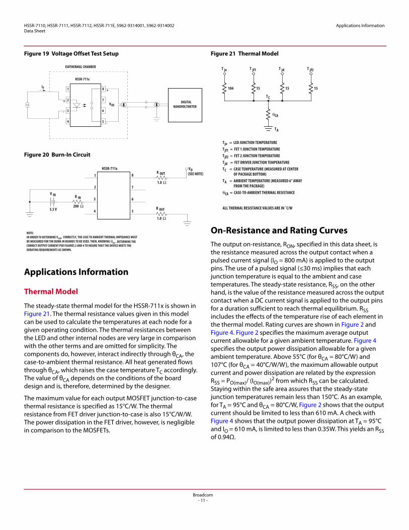
Figure 19 Voltage Offset Test Setup
Figure 20 Burn-In Circuit
Applications Information
Thermal Model
The steady-state thermal model for the HSSR-711x is shown in Figure 21. The thermal resistance values given in this model can be used to calculate the temperatures at each node for a given operating condition. The thermal resistances between the LED and other internal nodes are very large in comparison with the other terms and are omitted for simplicity. The components do, however, interact indirectly through θCA, the case-to-ambient thermal resistance. All heat generated flows through θCA, which raises the case temperature TC accordingly. The value of θCA depends on the conditions of the board design and is, therefore, determined by the designer.
The maximum value for each output MOSFET junction-to-case thermal resistance is specified as 15°C/W. The thermal resistance from FET driver junction-to-case is also 15°C/W/W. The power dissipation in the FET driver, however, is negligible in comparison to the MOSFETs.
Figure 21 Thermal Model
On-Resistance and Rating CurvesThe output on-resistance, RON, specified in this data sheet, is the resistance measured across the output contact when a pulsed current signal (IO = 800 mA) is applied to the output pins. The use of a pulsed signal (≤30 ms) implies that each junction temperature is equal to the ambient and case temperatures. The steady-state resistance, RSS, on the other hand, is the value of the resistance measured across the output contact when a DC current signal is applied to the output pins for a duration sufficient to reach thermal equilibrium. RSS includes the effects of the temperature rise of each element in the thermal model. Rating curves are shown in Figure 2 and Figure 4. Figure 2 specifies the maximum average output current allowable for a given ambient temperature. Figure 4 specifies the output power dissipation allowable for a given ambient temperature. Above 55°C (for θCA = 80°C/W) and 107°C (for θCA = 40°C/W/W), the maximum allowable output current and power dissipation are related by the expression RSS = PO(max)/ (IO(max))
2 from which RSS can be calculated. Staying within the safe area assures that the steady-state junction temperatures remain less than 150°C. As an example, for TA = 95°C and θCA = 80°C/W, Figure 2 shows that the output current should be limited to less than 610 mA. A check with Figure 4 shows that the output power dissipation at TA = 95°C and IO = 610 mA, is limited to less than 0.35W. This yields an RSS of 0.94Ω.
VOS
+
DIGITAL NANOVOLTMETER
ISOTHERMAL CHAMBER
HSSR-711x
2
3
4
1
6
7
5
8
-
IF
+
-
NOTE:IN ORDER TO DETERMINE VBE MEASURED FOR THE BURN-IN BOARDS TO BE USED. THEN, KNOWING CORRECT OUTPUT CURRENT PER FIGURES 2 AND 4 TO INSURE THAT THE DEVICE MEETS THEDERATING REQUIREMENTS AS SHOWN.
OUT CORRECTLY, THE CASE TO AMBIENT THERMAL IMPEDANCE MUST
CA , DETERMINE THE
2
3
4
1
6
7
5
8
R INV IN
5.5 V
1.0
R OUT
VO (SEE NOTE)
200
1.0
R OUTHSSR-711x
Tje = LED JUNCTION TEMPERATURE Tjf1 = FET 1 JUNCTION TEMPERATURETjf2 = FET 2 JUNCTION TEMPERATURETjd = FET DRIVER JUNCTION TEMPERATURETC = CASE TEMPERATURE (MEASURED AT CENTER
OF PACKAGE BOTTOM)TA = AMBIENT TEMPERATURE (MEASURED 6" AWAY
FROM THE PACKAGE)
CA = CASE-TO-AMBIENT THERMAL RESISTANCE
ALL THERMAL RESISTANCE VALUES ARE IN ˚C/W
T je
CA
104 15
TA
TC
T jdT jf1
1515
T jf2
Broadcom- 11 -
HSSR-7110, HSSR-7111, HSSR-7112, HSSR-711E, 5962-9314001, 5962-9314002Data Sheet
Design Considerations for Replacement of Electromechanical Relays
Design Considerations for Replacement of Electromechanical RelaysThe HSSR-711x family can replace electromechanical relays with comparable output voltage and current ratings. The following design issues need to be considered in the replacement circuit.
Input Circuit
The drive circuit of the electromechanical relay coil needs to be modified so that the average forward current driving the LED of the HSSR-711x does not exceed 20 mA. A nominal forward drive current of 10 mA is recommended. A recommended drive circuit with 5V VCC and CMOS logic gates is shown in Figure 1. If higher VCC voltages are used, adjust the current limiting resistor to a nominal LED forward current of 10 mA. One important consideration to note is that when the LED is turned off, no more than 0.6V forward bias should be applied across the LED. Even a few microamps of current may be sufficient to turn on the HSSR- 711x, although it may take a considerable time. The drive circuit should maintain at least 5 mA of LED current during the ON condition. If the LED forward current is less than the 5 mA level, it causes the HSSR-711x to turn on with a longer delay. In addition, the power dissipation in the output power MOSFETs increases, which, in turn, may violate the power dissipation guidelines and affect the reliability of the device.
Output Circuit
Unlike with electromechanical relays, when considering solid-state relays, the designer should pay careful attention to the output on-resistance. The previous section, On-Resistance and Rating Curves, describes the issues that need to be considered. In addition, for strictly dc applications, the designer has an advantage using Connection B, which has twice the output current rating as Connection A. Furthermore, for dc-only applications, with Connection B the on-resistance is considerably less when compared to Connection A.
Output over-voltage protection is yet another important design consideration when replacing electromechanical relays with the HSSR-711x. The output power MOSFETs can be protected using Metal oxide varistors (MOVs) or TransZorbs against voltage surges that exceed the 90V output withstand voltage rating. Examples of sources of voltage surges are inductive load kickbacks, lightning strikes, and electrostatic voltages that exceed the specifications on this data sheet. For more information on output load and protection, refer to Application Note 1047.
References Application Note 1047, Low On-Resistance Solid State Relays
for High Reliability Applications. Reliability Data for HSSR-7111, HSSR-7112, and HSSR-711E.
Broadcom- 12 -

For product information and a complete list of distributors, please go to our web site: www.broadcom.com.
Broadcom, the pulse logo, Connecting everything, Avago Technologies, Avago, and the A logo are among the trademarks of Broadcom in the United States, certain other countries and/or the EU.
Copyright © 2016–2017 Broadcom. All Rights Reserved.
The term "Broadcom" refers to Broadcom Limited and/or its subsidiaries. For more information, please visit www.broadcom.com.
Broadcom reserves the right to make changes without further notice to any products or data herein to improve reliability, function, or design.
Information furnished by Broadcom is believed to be accurate and reliable. However, Broadcom does not assume any liability arising out of the application or use of this information, nor the application or use of any product or circuit described herein, neither does it convey any license under its patent rights nor the rights of others.
AV02-3835EN – October 19, 2017