Embed Size (px)
Citation preview
����
81,9(56,7<�2)�9,&725,$'HSDUWPHQW�RI�(OHFWULFDO�(QJLQHHULQJ
(/(&������'HVLJQ�3URMHFW�����
������
6RIWZDUH�'HILQHG�5DGLR�6PDUWSKRQH�'HPRQVWUDWRU����������
$QGUHZ�/XQG�9��������%UHQGDQ�0RUJDQ�9��������+RZDUG�&KDQJ�9��������0DUN�0HVVPHU�9��������
Contents
List of Figures iii
Acknowledgments iv
Summary v
1 Introduction 1
2 Theory of Operation 4
2.1 Antenna and Amplifier . . . . . . . . . . . . . . . . . . . . . . 4
2.2 FPGA Digital Down Conversion . . . . . . . . . . . . . . . . . 6
2.2.1 Analog/Digital Interfaces . . . . . . . . . . . . . . . . . 6
2.2.2 FPGA . . . . . . . . . . . . . . . . . . . . . . . . . . . 7
2.2.3 Smartphone Communication . . . . . . . . . . . . . . . 9
2.2.4 PCB Design and Construction . . . . . . . . . . . . . . 9
2.3 SDR Android Application . . . . . . . . . . . . . . . . . . . . 10
2.3.1 User Interface . . . . . . . . . . . . . . . . . . . . . . . 11
2.3.2 Audio Sampling . . . . . . . . . . . . . . . . . . . . . . 12
2.3.3 Signal Processing and Output . . . . . . . . . . . . . . 13
3 Discussion 15
3.1 Problems Encountered . . . . . . . . . . . . . . . . . . . . . . 15
3.2 Future Improvements . . . . . . . . . . . . . . . . . . . . . . . 15
4 Applications 17
4.1 Aftermarket Accessory . . . . . . . . . . . . . . . . . . . . . . 17
i
4.2 Built-In Functionality . . . . . . . . . . . . . . . . . . . . . . . 18
5 Conclusions 19
A Circuit Schematic 20
B PCB Layout 21
C Bill of Materials 22
ii
List of Figures
1.1 Block diagram of SDRoid system . . . . . . . . . . . . . . . . 1
2.1 Demultiplexer circuit for resonant capacitance selection . . . . 5
2.2 Cascode amplifier circuit with 2.5V signal bias . . . . . . . . . 5
2.3 FPGA board . . . . . . . . . . . . . . . . . . . . . . . . . . . 6
2.4 Diagram of FPGA programming flow . . . . . . . . . . . . . . 8
2.5 DTMF signalling table . . . . . . . . . . . . . . . . . . . . . . 10
2.6 Application User Interface . . . . . . . . . . . . . . . . . . . . 11
A.1 Schematic of FPGA circuit . . . . . . . . . . . . . . . . . . . . 20
B.1 PCB layout of FPGA board . . . . . . . . . . . . . . . . . . . 21
C.1 FPGA circuit board Bill of Materials . . . . . . . . . . . . . . 22
iii
Acknowledgments
The authors would like to thank Dr. Peter Driessen for his guidance andsupport for this project. They would also like to thank Brent Sirna for hisknowledge and assistance.
iv
Summary
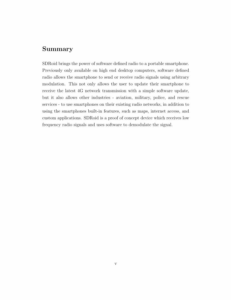
SDRoid brings the power of software defined radio to a portable smartphone.
Previously only available on high end desktop computers, software defined
radio allows the smartphone to send or receive radio signals using arbitrary
modulation. This not only allows the user to update their smartphone to
receive the latest 4G network transmission with a simple software update,
but it also allows other industries - aviation, military, police, and rescue
services - to use smartphones on their existing radio networks, in addition to
using the smartphones built-in features, such as maps, internet access, and
custom applications. SDRoid is a proof of concept device which receives low
frequency radio signals and uses software to demodulate the signal.
v
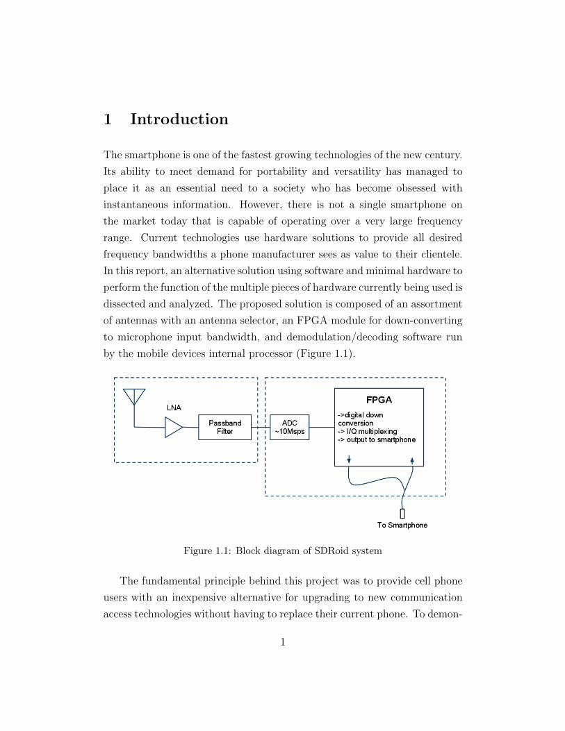
1 Introduction
The smartphone is one of the fastest growing technologies of the new century.
Its ability to meet demand for portability and versatility has managed to
place it as an essential need to a society who has become obsessed with
instantaneous information. However, there is not a single smartphone on
the market today that is capable of operating over a very large frequency
range. Current technologies use hardware solutions to provide all desired
frequency bandwidths a phone manufacturer sees as value to their clientele.
In this report, an alternative solution using software and minimal hardware to
perform the function of the multiple pieces of hardware currently being used is
dissected and analyzed. The proposed solution is composed of an assortment
of antennas with an antenna selector, an FPGA module for down-converting
to microphone input bandwidth, and demodulation/decoding software run
by the mobile devices internal processor (Figure 1.1).
Figure 1.1: Block diagram of SDRoid system
The fundamental principle behind this project was to provide cell phone
users with an inexpensive alternative for upgrading to new communication
access technologies without having to replace their current phone. To demon-
1
strate the functionality of this concept, an external device was developed to
perform the task of acquiring signals outside the current range of most smart-
phones such as AM (700 kHz 1.2 MHz) or RFID frequency (125 kHz) ranges.
The Samsung Galaxy S2 was used for demonstration due to open access to
its Android operating system. The basic operation of SDRoid works in the
following manner (each module will be discussed in detail in subsequent sec-
tions). The desired operation frequency is selected by the user through the
user interface on the mobile device. A tone pulse is then sent out through
the microphone port and pass through a multiplexer set the carrier frequency
the FPGA needs to down convert from. This tone pulse is also used to se-
lect the associated antenna, operating in the bandwidth in which the carrier
frequency falls in.
The signal is then acquired by the antenna and amplified to a voltage of
2.0 V peak-to-peak. To meet the FPGAs input specifications the signal was
then biased with 2.5 VDC. The FPGA takes this analog signal and converts
it to a digital signal then down-converts the signal to a baseband of 22 kHz.
The signal is then converted back to analog through the Digital-to-Analog
converter and sent to the microphone port of the mobile device. Taking
advantage of the processing capabilities of the mobile device, the signal is
demodulated by the software application (developed in Java for Android
environment). Once signal is processed it can then be displayed to text,
output to audio, captured to file, or modified (i.e. decryption) however the
user chooses to utilize the information.
Several engineering challenges needed to be overcome during this project.
Some of these challenges included: limited bandwidth capabilities of the mi-
crophone input maximum 44.1 kHz, sending signals from the mobile device
through the microphone port to the FPGA unit, analog only input/output of
the microphone port, setting bu↵er sizes of incoming data and frequency of
outputting data without noticeable lag or distortion, limited useable band-
width of certain antenna types, antenna signal gain control when dealing with
2
AM modulation schemes, and slower processing of Java written programs.
Using the microphone port lead to the majority of tradeo↵s considered on
this project.
The following report will focus on the operation and design of each of
the modules: antenna, FPGA, Android signal processing software, and the
Android application interface. In addition, the interfacing with each of the
modules will also be discussed. The vast majority of this project lies in its
software coding. With this in mind, the main blocks of code will be broken
down to assist anyone interested in understanding how the signal is processed
in both the FPGA and mobile device environments.
3
2 Theory of Operation
2.1 Antenna and Amplifier
In order for the device to obtain a signal over a wide range of frequencies,
multiple wide-band antennas need to be incorporated into the design. For
demonstration purposes AM range frequencies (700 kHz - 1.2 MHz) were
used. This frequency range was good for reducing some high frequency chal-
lenges but introduced a few other challenges not associated with the higher
frequencies and modulation schemes.
The antenna consists of a wire wrapped straight iron core. The wide
bandwidth of AM and relatively weak response of the antenna require a
variable capacitor to resonate the signal. In order to tune to the correct
frequency a signal from the phone would be needed to control the amount
of resonant capacitance. Although not perfect, it is possible to discretize
the range of bandwidth a resonant capacitance is set to. A single resonant
capacitance could cover a bandwidth of 100 kHz. The tone control sent
from the phone to the FPGA module could be used by a demultiplexer to
logically control a parallel set of resonant capacitors. For each 100 kHz range
the demultiplexer output would turn on a number of transistors operating in
switch mode to include the appropriate capacitance (Figure 2.1).
This demultiplexer would also be setup with controlling the switches on
which antenna should be used for other frequency bands such as FM, SW,
Bluetooth, etc. The FPGA signal input requirement is 2V peak-to-peak with
a DC o↵set of 2.5V. For AM frequency range standard NPN Bipolar junc-
tion transistors can be used for amplification. However for higher frequency
ranges, a cascode J-FET configuration is required to remove the Miller e↵ect
due to internal capacitance in the transistors. To maintain a good signal to
the FPGA an auto gain control for amplification is needed. This is especially
4
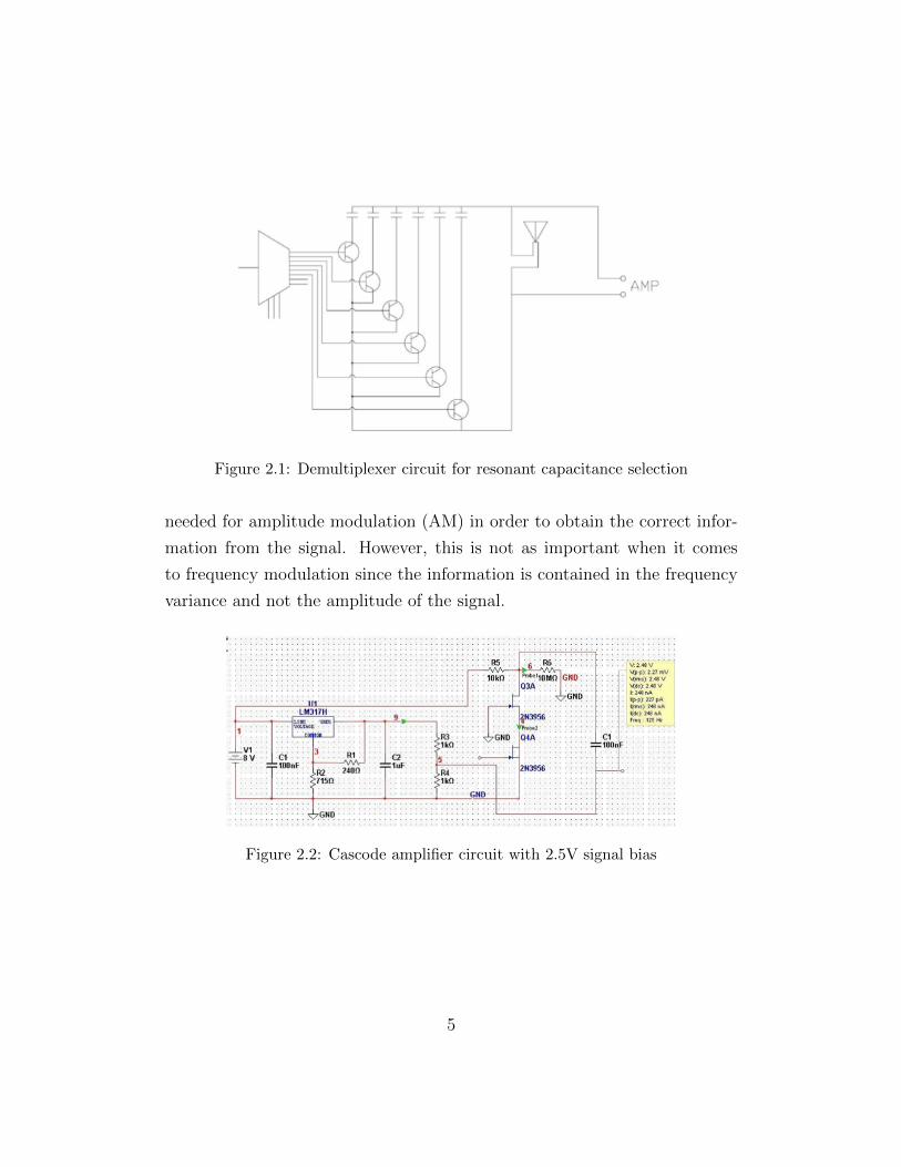
Figure 2.1: Demultiplexer circuit for resonant capacitance selection
needed for amplitude modulation (AM) in order to obtain the correct infor-
mation from the signal. However, this is not as important when it comes
to frequency modulation since the information is contained in the frequency
variance and not the amplitude of the signal.
Figure 2.2: Cascode amplifier circuit with 2.5V signal bias
5
2.2 FPGA Digital Down Conversion
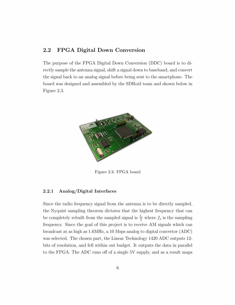
The purpose of the FPGA Digital Down Conversion (DDC) board is to di-
rectly sample the antenna signal, shift a signal down to baseband, and convert
the signal back to an analog signal before being sent to the smartphone. The
board was designed and assembled by the SDRoid team and shown below in
Figure 2.3.
Figure 2.3: FPGA board
2.2.1 Analog/Digital Interfaces
Since the radio frequency signal from the antenna is to be directly sampled,
the Nyquist sampling theorem dictates that the highest frequency that can
be completely rebuilt from the sampled signal is fs2 where fs is the sampling
frequency. Since the goal of this project is to receive AM signals which can
broadcast at as high as 1.6MHz, a 10 Msps analog to digital convertor (ADC)
was selected. The chosen part, the Linear Technology 1420 ADC outputs 12-
bits of resolution, and fell within out budget. It outputs the data in parallel
to the FPGA. The ADC runs o↵ of a single 5V supply, and as a result maps
6
a 2.5V signal to a value of 0, a 5V signal to a value of 2047, and a 0V signal
to -2048.
The digital to analog convertor (DAC) which converts the baseband sig-
nal to an analog signal before getting sent to the smartphone has much lower
requirements. Since the smartphone microphone input usually samples at a
maximum of 48kHz, having a DAC with a higher settling time would provide
little benefit. The National Semiconductor DAC121S was chosen because,
like the ADC, it supported 12-bit resolution, and due to it’s small footprint,
low pin count, and low power requirements. Additionally, the same DAC
was used in an accessory DAC component for the FPGA demo board used
for early prototyping, saving valuable development time. The DAC commu-
nicates with the FPGA using a serial SPI interface. Since the DAC outputs
a 0-3.3V signal, it is reduced using a voltage divider, and the DC o↵set is
removed using a capacitor before going to the microphone port.
2.2.2 FPGA
The FPGA is tasked with receiving the ADC signal, shifting 22kHz of band-
width down to baseband, and sending the signal to the DAC. The exact
22kHz of bandwidth to be sent is defined by the user through the app on the
smartphone.
To preform these tasks, the FPGA must be able to implement a Direct
Digital Synthesizer (DDS) which can generate a digital sine and cosine of
configurable frequency, a digital finite impulse response (FIR) filter, and all
of the interfaces to external ICs. For this purpose, a Xilinx Spartan-3E FPGA
was selected. In addition to fulfilling the above requirements, the FPGA also
features 250 million gates - enough for all the entire program - on a 144-pin
hand-solderable package.
The FPGA programming was all done in the Xilinx IDE. The lowpass
7
FIR filters were written in verilog and generated using Xilinx’s highly opti-
mized filter compiler. The interfaces to the DAC and DTMF detector ICs
(see section 2.2.3) were written in Verilog by hand, and the DDS and clock
managers (used to generate clock signals besides the 50MHz primary clock)
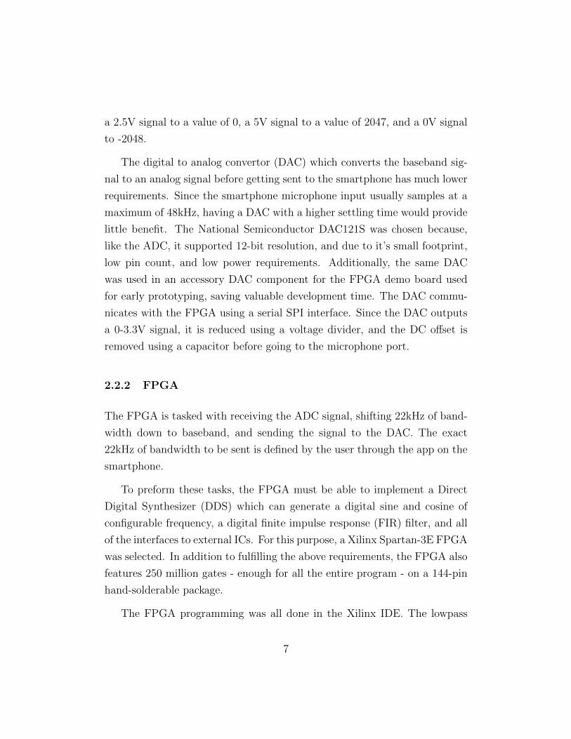
were provided by Xilinx. The component OSC1 is a 50MHz oscillator acting
as the system clock for the FPGA.
Figure 2.4: Diagram of FPGA programming flow
As FPGAs do not have solid state memory, the programming must be
loaded every time on power up. For testing, the JTAG connector was used to
program the FPGA, however a programmable read-only memory (PROM) IC
with 2MB of program memory was included on the circuit board for simplicity
- the PROM loads the program bitstream onto the FPGA automatically
on power up. The PROM or JTAG functionality is selected using the two
jumpers J3 and J4.
The FPGA requires three di↵erent voltage supplies - 1.2V, 2.5V and 3.3V.
The 1.2V and 2.5V source are used internally for device power, and the 3.3V
supply is used to power the input and output (I/O) pins.
8
2.2.3 Smartphone Communication
Due to the limited bandwidth analog channel between the FPGA board and
the smartphone, communication between the two is di�cult. Since the head-
phone port is used we are limited to one audio channel going from the FPGA
to the phone using the phone’s microphone port, and two audio channels go-
ing from the smartphone to the FPGA board. Unfortunately, our application
needs the opposite - 2 channels from the FPGA board for in-phase (I) and
quadrature (Q) signals, and 1 channel going to the FPGA board for tuning
information. The FPGA uses the following equation for calculating the 27
bit value for the DDS.
fDDS =ftune227
fclk(2.1)
We made due with only the I channel being sent from the smartphone,
which made the radio try sensitive to frequency error. To send the tuning
information from the smartphone app to the FPGA board, dual tone multi-
frequency (DTMF) signalling was used. DTMF signals are commonly heard
on touch tone phones - a tone composed of 2 frequencies is mapped to a
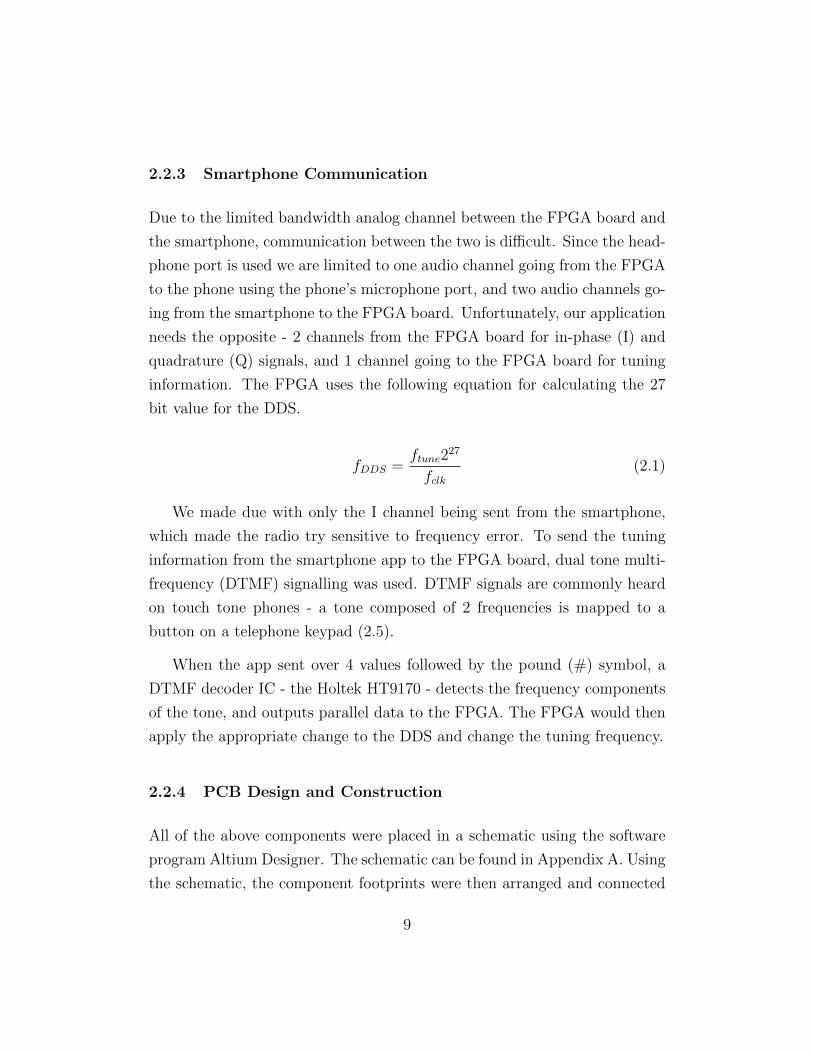
button on a telephone keypad (2.5).
When the app sent over 4 values followed by the pound (#) symbol, a
DTMF decoder IC - the Holtek HT9170 - detects the frequency components
of the tone, and outputs parallel data to the FPGA. The FPGA would then
apply the appropriate change to the DDS and change the tuning frequency.
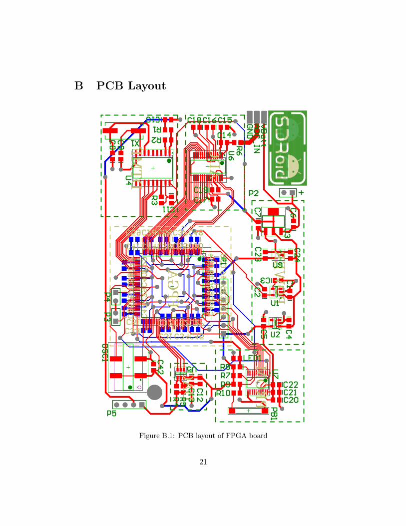
2.2.4 PCB Design and Construction
All of the above components were placed in a schematic using the software
program Altium Designer. The schematic can be found in Appendix A. Using
the schematic, the component footprints were then arranged and connected
9
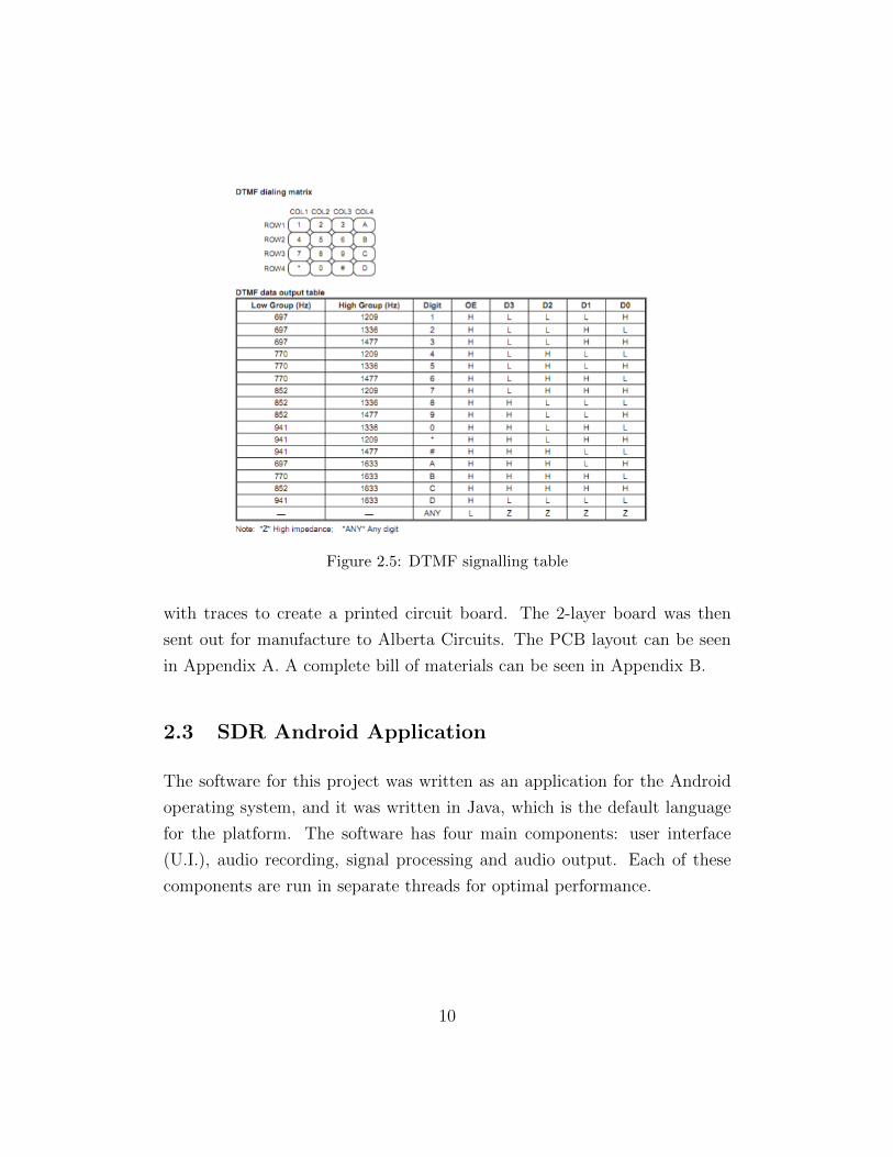
Figure 2.5: DTMF signalling table
with traces to create a printed circuit board. The 2-layer board was then
sent out for manufacture to Alberta Circuits. The PCB layout can be seen
in Appendix A. A complete bill of materials can be seen in Appendix B.
2.3 SDR Android Application
The software for this project was written as an application for the Android
operating system, and it was written in Java, which is the default language
for the platform. The software has four main components: user interface
(U.I.), audio recording, signal processing and audio output. Each of these
components are run in separate threads for optimal performance.
10
2.3.1 User Interface
The U.I. thread is where the users interacts with the app; the design of this
can be seen in Figure 2.6. The user is prompted for a modulation type,
and based on their input, is able to provide additional information. For this
project, only AM demodulation and voice playback were implemented, but
additional modulation schemes, such as FSK for low freqeuncy RFID, only
require software updates in order to become functional.
Figure 2.6: Application User Interface
Supposing the user chooses AM demodulation, he is then prompted for a
frequency. Once the frequency is chosen, the phone produces a dial tone that
11
is transmitted along the headphone wire to the FPGA as a control signal;
the handling of which can be seen in the FPGA section of this report. The
U.I. thread then creates a new thread for handling the audio data that is
transmitted from the FPGA back to the smartphone.
2.3.2 Audio Sampling
Based on the modulation scheme chosen by the user a new abstract AudioIn
object is created to perform audio recording. More specifically, the object
that is created is the subclass of AudioIn that corresponds to the modulation
scheme chosen by the user. The purpose of having a single abstract parent
class with multiple child subclasses is to guaruntee that all recording classes
can be interacted with using the same methods. This ensures the system is
scalable when new modulation schemes are introduced.
AudioIn and all of its subclasses extend the Java Thread class, so they
are run in a separate thread, which allows for computations performed by
the AudioIn subclass to run in parallel with U.I. activities. This prevents
the application from appearing frozen or bogged down when it is performing
the relatively processor expensive recording or signal processing tasks. The
particular smartphone that was used for designing this application has a
dual core processor, so another benefit of this multithreading approach is
that both processor cores are engaged.
When the AudioIn subclass thread is started, it begins sampling from
the microphone input at a frequency of 44.1kHz at 16 bits per sample. This
sampling rate is required to ensure that the entire incoming signal can be
sampled, as AM waves have a bandwidth of 10kHz, and is the highest sup-
ported sampling rate for Android phones. This restriction is part of the
reason that digital downsamlping performed by the FPGA is required. As
each short is recorded, it is immediately pushed to a Concurrent Queue that
12
is part of the Modulate object. By passing of the data to another thread for
processing, the AudioIn subclass remains available to sampling.
2.3.3 Signal Processing and Output
During initialization, the AudioIn subclass creates and runs the third thread
object, known as Modulate. Modulate in turn has several subclasses which
are catered for the di↵erent types of modulation available, and they all extend
the Java Thread class. Again this parent-child subclass structuring is to
ensure that the system is easily scalable. In turn, during its own initialization,
the Modulate object creates the final thread, which is the AudioOut object.
This class does not have any subclasses as there is only one audio output
option. However, since not all wireless data carries audio information, further
classes would need to be created to handle the output data to the U.I. thread,
such as for data carried by FSK for RFID.
The Modulate subclass that was invoked for a given modulation type
waits for data to enter the Concurrent Queue from the AudioIn thread, re-
moves the sample from the front of the queue, performs the required de-
modulation and then places the processed data into a Concurrent Queue in
the AudioOut object. The use of Concurrent Queues is necessary, as the
queues need to stay synchronized between the separate threads. In turn the
AudioOut object waits for data to enter its queue, before writing it to the
speakers. Separating the Modulate and AudioOut processes and queues into
separate Threads is to ensure that there is no latency in outputting to the
speakers while processing the data.
The signal processing that is required depends on the modulation scheme.
For AM demodulation, the only processing required is a low pass filter. This
is because the digital down conversion done by the FPGA to bring the radio
wave down to baseband is essentially performing AM demodulation. The
13
lowpass filter used is a fifth order Butterworth filter. The transfer function
which describes this filter is changed to the di↵erence equation form so that
is can be applied by multiplying present and past value of the sampled audio
stream by the filter coe�cients. The transfer function for the low pass filter
used can be seen in Equation 2.2.
H(z) =0.036 + 0.18z�1 + 0.36z�2 + 0.36z�3 + 0.18z�4 + 0.036z�5
1� 0.458z�1 + 0.707z�2 � 0.160z�3 + 0.067z�4 � 0.004z�5(2.2)
14
3 Discussion
3.1 Problems Encountered
There were many issues encountered during the production of this system.
We have listed here some of the most prominent ones here. The audio jack of
the cell phone only has mono input, limiting the output of the FPGA board
to only In-Phase data meaning the AM signal went in and out of phase due
to slight frequency error. A small manufacturing defect on the PCB caused
a short circuit which slowed down progress. An unknown error, potentially
electrostatic discharge (ESD), caused a FPGA failure. Although the cause
of the failure was never determined, the second FPGA never experienced the
same failure.
For the software portion of the project, introducing multithreading was
absolutely necessary to the usability of the application, but coding it was very
frustrating. Also, controlling the input and output through the microphone
and speakers in the audio jack imposes some unnecessary restrictions. In
addition to the mono input, the sampling rate has a maximum rate of 44kHz,
meaning the incoming or outgoing signal can only have a bandwidth of 22kHz.
Finally, while low pass filtering in Java could be done in near real time, more
intense software demodulation could be weighed down by the overhead of
Java.
3.2 Future Improvements
For higher frequency applications in the MHz or Ghz range, directly sampling
with a ADC becomes impractical. Much like the USRP does, a future im-
provement could be to use an intermediate frequency in the radio frequency
stage to reduce the frequency before sampling. As ADCs are rapidly becom-
15
ing faster, cheaper, and with higher resolution, a 200 Msps ADC would best
be included on a future product.
Shortly after the project was started, Google announced the release of
the Open Accessory Development Kit (ADK). This allows android devices
to act as either a USB host or a USB accessory. Unfortunately, at release
this API was only available for Android 3.1 when the project was started,
which is the tablet version of the operating system. The smartphone we had
was only capable of running Android 2.3.3, and significant design work had
already been done which focused on using the audio jack for data transfer. A
significant future improvement would be to use the USB port for data transfer
between the phone and the FPGA. This would allow for bandwidth larger
than 22kHz, which is required for some wireless protocols; prevent the need
for data to be converted from digital to analog and back when sending data
between the phone and the FPGA; and allow for full duplex communication
between the phone and FPGA.
Demodulation of the audio signal is the most processor intensive portion
of the signal processing, and it is currently implemented in Java, which has
a lot of overhead. The Android Native Developer Kit (NDK) allows the
programmer to access Java Native Interface (JNI), which in turn allows Java
to interact directly with native code such as C or C++. Using the NDK,
computationally expensive portions of the program, such as demodulation,
could be written in C++ for higher e�ciency. As a trade o↵, the complexity
of the program would increase significantly, which is why this is marked as
future work.
16
4 Applications
SDRoid demonstrates that the requirements for software defined radio can
be fulfilled on present-generation smartphones. This capability is envisioned
as having two primary commercial applications: being packaged as an after-
market accessory for current smartphones, or being implemented inside of
the next generation of smartphones.
4.1 Aftermarket Accessory
As an external unit this device can act as upgrade interface unit providing
current smartphone users the ability to upgrade to the future 4G network.
In addition, users could expand their phones functionality by accessing Blue-
tooth, AM, FM and even shortwave communications.
Many industries are now trying to use smartphones since they o↵er an
easy to use interface, and o↵er excellent functionality - GPS, maps, voice
calling, custom applications, etc. The unit could be used by police or emer-
gency personnel, integrating their radio devices with location data. Search
and Rescue could sweep a wide range of frequencies in an attempt to get
or receive a signal from di↵erent frequency ranges. It may be possible that
someone could transmit/receive a signal at a lower frequency where a higher
frequency would be attenuated too much.
Recently, the US army has begun a pilot program where they provide each
soldier with an Android or iPhone device. They found that using consumer
devices such as smartphones for GPS, information dispersion, and communi-
cation is cost-e�cient, requires less training to use, and reduces the amount
of equipment carried by the soldier. A SDRoid attachment could replace
the soldiers radio, since it allows for the military to implement their own
encryption, and maintains compatibility with existing radio infrastructure.
17
4.2 Built-In Functionality
Much like an aftermarket accessory, SDR, if implemented inside of future
smartphones, allows the handset to remain compatible with future standards
for much longer than typical smartphones with hardware radios. For exam-
ple, if the Bluetooth 4.0 specification gets an enhancement which allows
for much higher transfer speeds, as long as the operating frequency hasn’t
changed (i.e. the antenna itself is still compatible) then the SDR can easily
support the new standard with a software upgrade.
18
5 Conclusions
The goal of this project is to provide cell phone users with an inexpensive
alternative for upgrading to new communication access technologies without
having to replace their current phone. The results for our project is satisfied
but can be improved. We managed to receive AM and voice signal for our
android app. The android app UI and FPGA board was designed and tested
which are working properly. Unfortunatly, due to the time limit, the FPSK
antenna and FPSK code translation is not completed but it can be modi-
fied and implemented into our project. Also, for future development, other
demodulation type such as FM can be added for further usage.
19
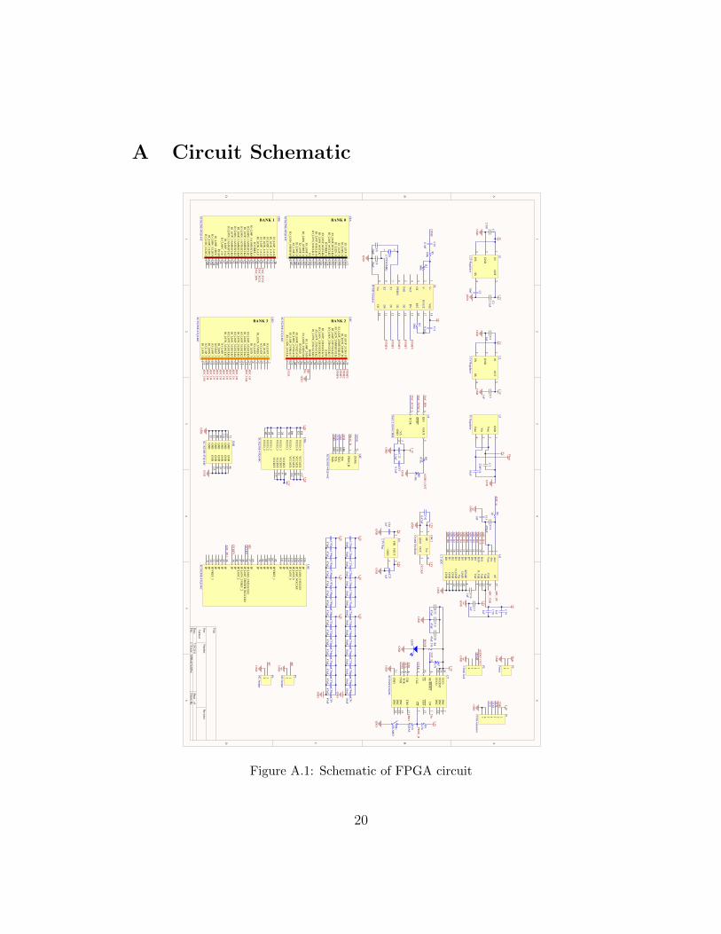
A Circuit Schematic
1 1
2 2
3 3
4 4
5 5
6 6
DD
CC
BB
AA
Title
Num
berRevision
SizeTabloid
Date:
7/28/2011Sheet of
File:C:\U
sers\..\SDRoid.SchD
ocDraw
n By:
IN1
GND
2
EN3
SS4
OUT
5U1
1.2V Regulator
5V1.2V
GND
2.2uF C1
2.2uFC2
10nF C3
GND
IN1
GND
2
EN3
SS4
OUT
5U2
3.3V Regulator
1uFC4
1uF
C5
GND
GND
5V3.3V
22uF
C7
10uF
C6
GND
5V Vbatt
Vss
9OE
10
D0
11
D1
12
D2
13
D3
14
DV
15
EST16
RT/G
T17
Vdd
18Va
1
V-
2
GS
3
Vref
4
INH
5
PWDN
6
X1
7
X2
8
U4
DTM
F Detector
20pFC8
20pFC9
0.1uF
C10
0.1uF
C11
1 2
X1
3.579545MHz
GND
R1
100kR2
100kR3
300k
DTM
F
5V
DTM
FV
DTM
F3
DTM
F2
DTM
F1
DTM
F0
VOUT
1
GND
2VA
3
DIN
4
SCLK5
SYNC
6
U5
DAC121S101CIM
K
3.3V
2.2uFC12
0.1uFC13
DAC_D
IN
DAC_SY
NC
DAC_SCLK
AUDIO_O
UT
R4
93.1kR5
1.43k
GND
GND
ADC_D
11ADC_D
10ADC_D
9ADC_D
8ADC_D
7ADC_D
6ADC_D
5ADC_D
4ADC_D
3ADC_D
2ADC_D
1ADC_D
0
GND
D5
15
D4
16
D3
17
D2
18
D1
19
D0
20
O_G
ND
21
O_V
dd22
Vdd
23
GND
24
Vss
25
CLK26
OF
27
GAIN
28D6
14D7
13D8
12D9
11D10
10D11
9
GND
8
Vdd
7
GND
6
Vref
5
SENSE
4
Vcm
3Ain-
2Aina
1U6
LT ADC
R6
30
470pFC14
1uF
C15
GND
1uF
C18
1uF
C19
1uFC16
1uFC17
ADC_in
3.3V
GND 5V
ADC_CLK
ADC_O
F
D0
1
DNC
2
CLK3
TDI
4
TMS
5TCK
6
CF7
OE/RESET
8
DNC
9
CE10
GND
11
DNC
12
CEO13
DNC
14
DNC
15
DNC
16
TDO
17
VCCIN
T18
VCCO
19
VCCJ
20U7
XCF02SV
OG20C
3.3V
GND
CCLK
DONE
INIT_B
R7
4.7kR8
330
TDO
jTCKjTM
S
jTDO
Din
PROG_B
R9
4.7k
3.3V
1234567
P1JTAG connector
3.3V
jTMS
jTCKjTD
OjTD
IGND
PB1
SW-SPST
GND R10
ERAS
LED1G
ND
12
P2Power
Vbatt
GND
BANK a
IO_L10N
_0/HSW
AP
143IO_L10P_0
142IO_L09N
_0140
IO_L09P_0
139IO_L08N
_0/VREF_0
135IO_L08P_0
134IO
132IO_L07N
_0/GCLK
11131
IO_L07P_0/G
CLK10
130IO_L05N
_0/GCLK
7126
IO_L05P_0/G
CLK6
125IO/VREF_0
124IO_L04N
_0/GCLK
5123
IO_L04P_0/G
CLK4
122IO_L02N
_0117
IO_L02P_0
116IO_L01N
_0113
IO_L01P_0
112U8A
XC3S250E-4TQ
144C
BANK 1
IO_L10N
_1/LDC2
106IO_L10P_1/LD
C1105
IO_L09N
_1/LDC0
104IO_L09P_1/H
DC
103IO/A0
98IO_L08N
_1/A1
97IO_L08P_1/A
296
IO_L07N
_1/A3/R
HCLK
794
IO_L07P_1/A
4/RHCLK
693
IO_L06N
_1/A5/R
HCLK
592
IO_L06P_1/A
6/RHCLK
491
IO_L05N
_1/A7/R
HCLK
388
IO_L05P_1/A
8/RHCLK
287
IO_L04N
_1/A9/R
HCLK
186
IO_L04P_1/A
10/RHCLK
085
IO/VREF_1
83IO_L03N
_1/A11
82IO_L03P_1/A
1281
IO_L02N
_1/A13
77IO_L02P_1/A
1476
IO_L01N
_1/A15
75IO_L01P_1/A
1674
U8B
XC3S250E-4TQ
144C
BANK 2
IO_L10N
_2/CCLK71
IO_L10P_2/V
S0/A17
70IO_L09N
_2/VS1/A
1868
IO_L09P_2/V
S2/A19
67IO/VREF_2
66IO_L08N
_2/DIN/D0
63IO_L08P_2/M
062
IO/M
160
IO_L07N
_2/D1/G
CLK3
59IO_L07P_2/D
2/GCLK
258
IO_L05N
_2/D3/G
CLK15
54IO_L05P_2/D
4/GCLK
1453
IO/D5
52IO_L04N
_2/D6/G
CLK13
51IO_L04P_2/D
7/GCLK
1250
IO_L02N
_2/MOSI/CSI_B
44IO_L02P_2/D
OUT/BU
SY43
IO_L01N
_2/INIT_B
40IO_L01P_2/C
SO_B
39U8C
XC3S250E-4TQ
144C
BANK 3
IO_L10N
_335
IO_L10P_3
34IO_L09N
_333
IO_L09P_3
32IO/VREF_3
31IO_L08N
_326
IO_L08P_3
25IO_L07N
_3/LHCLK
723
IO_L07P_3/LH
CLK6
22IO_L06N
_3/LHCLK
521
IO_L06P_3/LH
CLK4
20IO_L05N
_3/LHCLK
317
IO_L05P_3/LH
CLK2
16IO_L04N
_3/LHCLK
115
IO_L04P_3/LH
CLK0
14IO_L03N
_38
IO_L03P_3
7IO_L02N
_3/VREF_3
5IO_L02P_3
4IO_L01N
_33
IO_L01P_3
2U8D
XC3S250E-4TQ
144C
IP141
IP111
IP114
IP_L03P_0119
IP_L03N_0
120IP_L06P_0/G
CLK
8128
IP_L06N_0/G
CLK9
129IP
136
IP78
IP84
IP89
IP101
IP107
IP/VREF_1
95
IP38
IP41
IP_L03P_247
IP_L03N_2/V
REF_248
IP_L06P_2/RDWR_B
/GCLK
056
IP_L06N_2/M
2/GCLK
157
IP69
IP6
IP10
IP/VREF_3
12IP
18IP
24IP
29IP
36
U8E
XC3S250E-4TQ
144C
DONE
72
PROG_B
1
TCK110
TDI
144
TDO
109
TMS
108
U8F
XC3S250E-4TQ
144C
VCCA
UX
137
VCCA
UX
65
VCCA
UX
30
VCCA
UX
102
VCCIN
T80
VCCIN
T9
VCCIN
T45
VCCIN
T115
VCCO
_0138
VCCO
_0121
VCCO
_1100
VCCO
_179
VCCO
_242
VCCO
_264
VCCO
_249
VCCO
_313
VCCO
_328
U8G
XC3S250E-4TQ
144C
GND
133GND
11GND
19GND
27GND
37GND
46
GND
55GND
61GND
90GND
99GND
118GND
127GND
73U8H
XC3S250E-4TQ
144CGND
GND
DONE
PROG_B
jTDI
TDO
jTCKjTM
S
47nFC20
47nFC21
47nFC22
GND
GND
1
VOUT
2VIN
3U9
2.5V Reg
5V2.5V
1uFC23
1uFC24
GND
1.2V
2.5V3.3V
10nFC25
10nFC26
10nFC27
10nFC28
10nFC29
10nFC30
10nFC31
10nFC32
10nFC33
10nFC34
10nFC35
10nFC36
10nFC37
10nFC38
10nFC39
10nFC40
10nFC41
47nFC43
47nFC44
47nFC45
47nFC46
47nFC47
47nFC48
47nFC49
47nFC50
47nFC51
47nFC52
47nFC53
47nFC54
47nFC55
47nFC56
47nFC57
47nFC58
47nFC59
GND
GND
0.47uFC42
2.5V1.2V
3.3V
2.5V1.2V
3.3V
GND
2
OE
1Vcc
4
OUT
3
OSC1
Crystal Oscillator
3.3V3.3V
GND
GCLK
0
GCLK
0
CCLK
GND
12
P3M0 Jum
per
M0
M2
M0GND
12
P4M2 Jum
per
M2
GND
GND
DTM
FV
DTM
F3DTM
F2DTM
F1DTM
F0
ADC_D
11
ADC_D
10ADC_D
9ADC_D
8ADC_D
7ADC_D
6ADC_D
5ADC_D
4ADC_D
3ADC_D
2ADC_D
1ADC_D
0
DAC_SY
NC
DAC_SCLK
DAC_D
IN
1234
P53.5mm Jack
AUDIO_O
UT
DTM
F
GND
Din
ADC_O
FADC_CLK
GND
1
Vout
2
Vin
3
Vout
4
U3
5V Regulator
Figure A.1: Schematic of FPGA circuit
20
B PCB Layout
PAC101PAC102
COC1
PAC201PAC202COC2
PAC301PAC302
COC3
PAC401PAC402COC4
PAC501PAC502COC5
PAC601PAC602
COC6PAC701PAC702COC7
PAC801PAC802
COC8PAC901
PAC902COC9
PAC1001PAC1002
COC10PAC1101PAC1102COC11
PAC1201PAC1202COC12PAC1301PAC1302COC13
PAC1401PAC1402
COC14PAC1501PAC1502
COC15PAC1601PAC1602
COC16PAC1701PAC1702
COC17PAC1801PAC1802
COC18PAC1901PAC1902
COC19
PAC2002PAC2001
COC20PAC2102PAC2101COC21
PAC2202PAC2201
COC22PAC2302
PAC2301COC23 PAC2402
PAC2401COC24
PAC2502PAC2501COC25
PAC2602PAC2601
COC26
PAC2702PAC2701 COC27
PAC2802PAC2801COC28
PAC2902PAC2901
COC29
PAC3002PAC3001
COC30
PAC3102PAC3101COC31
PAC3202PAC3201COC32PAC3302
PAC3301
COC33 PAC3402PAC3401 COC34
PAC3502PAC3501COC35
PAC3602PAC3601
COC36
PAC3702PAC3701
COC37PAC3802PAC3801
COC38PAC3902
PAC3901COC39
PAC4002PAC4001COC40
PAC4102PAC4101
COC41PAC4202
PAC4201COC42
PAC4302PAC4301COC43
PAC4402PAC4401
COC44
PAC4502PAC4501 COC45
PAC4602PAC4601COC46
PAC4702PAC4701
COC47
PAC4802PAC4801
COC48PAC4902PAC4901COC49PAC5002PAC5001COC50
PAC5102PAC5101
COC51
PAC5202PAC5201 COC52
PAC5302PAC5301COC53
PAC5402PAC5401
COC54
PAC5502PAC5501
COC55PAC5602PAC5601
COC56
PAC5702PAC5701
COC57PAC5802PAC5801
COC58PAC5902PAC5901
COC59
PALED101PALED102
COLED1
PAOSC101PAOSC102
PAOSC104PAOSC103
COOSC1
PAP103PAP101
PAP102PAP104
PAP105PAP106
PAP107COP1
PAP202PAP201
COP2
PAP302PAP301COP3
PAP402PAP401COP4
PAP504PAP503PAP502PAP501COP5 PAPB102
PAPB101COPB1
PAR101PAR102
COR1PAR201PAR202
COR2PAR301PAR302COR3
PAR401PAR402COR4PAR501PAR502COR5
PAR601PAR602 COR6
PAR701PAR702
COR7PAR801PAR802
COR8PAR901PAR902
COR9PAR1001PAR1002
COR10
PAU105PAU104 PAU103PAU102PAU101COU1
PAU205PAU204 PAU203PAU202PAU201COU2
PAU301
PAU302
PAU303
PAU304COU3
PAU401PAU402PAU403PAU404PAU405PAU406PAU407PAU408PAU409
PAU4018PAU4017PAU4016PAU4015PAU4014PAU4013PAU4012PAU4011PAU4010
COU4
PAU501PAU502PAU503
PAU504PAU505PAU506
COU5PAU6015PAU6016PAU6017PAU6018PAU6019PAU6020PAU6021PAU6022PAU6023PAU6024PAU6025PAU6026PAU6027PAU6028
PAU6014PAU6013PAU6012PAU6011PAU6010PAU609PAU608PAU607PAU606PAU605PAU604PAU603PAU602PAU601
COU6
PAU7011PAU7012PAU7013PAU7014PAU7015PAU7016PAU7017PAU7018PAU7019PAU7020
PAU7010PAU709PAU708PAU707PAU706PAU705PAU704PAU703PAU702PAU701
COU7
PAU801PAU802PAU803PAU804PAU805PAU806PAU807PAU808PAU809PAU8010PAU8011PAU8012PAU8013PAU8014PAU8015PAU8016PAU8017PAU8018PAU8019PAU8020PAU8021PAU8022PAU8023PAU8024PAU8025PAU8026PAU8027PAU8028PAU8029PAU8030PAU8031PAU8032PAU8033PAU8034PAU8035PAU8036PAU8037PAU8038PAU8039PAU8040PAU8041PAU8042PAU8043PAU8044PAU8045PAU8046PAU8047PAU8048PAU8049PAU8050PAU8051PAU8052PAU8053PAU8054PAU8055PAU8056PAU8057PAU8058PAU8059PAU8060PAU8061PAU8062PAU8063PAU8064PAU8065PAU8066PAU8067PAU8068PAU8069PAU8070PAU8071PAU8072
PAU8073PAU8074PAU8075PAU8076PAU8077PAU8078PAU8079PAU8080PAU8081PAU8082PAU8083PAU8084PAU8085PAU8086PAU8087PAU8088PAU8089PAU8090PAU8091PAU8092PAU8093PAU8094PAU8095PAU8096PAU8097PAU8098PAU8099PAU80100PAU80101PAU80102PAU80103PAU80104PAU80105PAU80106PAU80107PAU80108
PAU80109PAU80110PAU80111PAU80112PAU80113PAU80114
PAU80115PAU80116PAU80117PAU80118PAU80119PAU80120
PAU80121PAU80122PAU80123PAU80124PAU80125PAU80126
PAU80127PAU80128PAU80129PAU80130PAU80131PAU80132
PAU80133PAU80134PAU80135PAU80136PAU80137PAU80138
PAU80139PAU80140PAU80141PAU80142PAU80143PAU80144
COU8 PAU903PAU902PAU901
COU9
PAX101PAX102COX1
PAC201
PAC2902
PAC3002
PAC3102PAC3202
PAC4702
PAC4802
PAC4902
PAC5002
PAU105
PAU809
PAU8045
PAU8080
PAU80115
PAC2302
PAC2502
PAC2602
PAC2702PAC2802
PAC4302
PAC4402
PAC4502
PAC4602
PAU8030
PAU8065
PAU80102
PAU80137
PAU902
PAC502
PAC1201PAC1301
PAC1702
PAC2002PAC2102
PAC2202
PAC3302
PAC3402
PAC3502PAC3602
PAC3702
PAC3802
PAC3902PAC4002
PAC4102
PAC4202PAC5102
PAC5202
PAC5302PAC5402
PAC5502
PAC5602
PAC5702PAC5802
PAC5902PAOSC101PAOSC104
PAP101PAR702
PAR802PAR902
PAU205
PAU503
PAU6022
PAU7018PAU7019PAU7020
PAU8013
PAU8028
PAU8042PAU8049
PAU8064
PAU8079
PAU80100
PAU80121PAU80138
PAC101PAC402
PAC701
PAC1102
PAC1801
PAC1901
PAC2402PAU101
PAU103PAU201
PAU203PAU302
PAU304
PAU4018
PAU607PAU6023
PAU903
PAU6026
PAU8015
PAU6020
PAU8020
PAU6019
PAU8021
PAU6018
PAU8022
PAU6017
PAU8023
PAU6016
PAU8025
PAU6015
PAU8026
PAU6014
PAU8031
PAU6013
PAU8032
PAU6012
PAU8033
PAU6011
PAU8034
PAU6010
PAU8035
PAU609
PAU8036
PAR601
PAU6027
PAU8014
PAP501
PAR402 PAR502
PAU703
PAU8071
PAU504
PAU8083
PAU505
PAU8082
PAU506
PAU8081
PAU701
PAU8063
PALED101PAR801 PAU7010
PAU8072
PAC1002
PAP502PAU4011
PAU8044PAU4012
PAU8043PAU4013
PAU8040
PAU4014
PAU8039
PAU4015
PAU8038
PAOSC103PAU8056 PAC102
PAC202
PAC302PAC401PAC501
PAC602PAC702
PAC801 PAC901
PAC1202PAC1302
PAC1501
PAC1601PAC1701
PAC1802
PAC1902
PAC2001PAC2101
PAC2201
PAC2301 PAC2401
PAC2501
PAC2601
PAC2701
PAC2801
PAC2901
PAC3001
PAC3101PAC3201
PAC3301
PAC3401
PAC3501PAC3601
PAC3701
PAC3801
PAC3901PAC4001
PAC4101
PAC4201
PAC4301PAC4401
PAC4501
PAC4601
PAC4701
PAC4801PAC4901 PAC5001
PAC5101
PAC5201
PAC5301PAC5401
PAC5501
PAC5601
PAC5701PAC5801
PAC5901
PALED102
PAOSC102
PAP106PAP107
PAP202
PAP302PAP402
PAP504 PAPB101
PAR501
PAU102PAU202
PAU301
PAU409
PAU502
PAU604PAU606PAU608
PAU6021
PAU6024PAU6025
PAU6028
PAU7011
PAU8011
PAU8019
PAU8027PAU8037PAU8046
PAU8055PAU8060PAU8061
PAU8073
PAU8090
PAU8099
PAU80118PAU80127
PAU80133
PAU901
PAR701
PAU708
PAP103
PAU706
PAU80110
PAP105
PAU80144
PAP104
PAU7017
PAP102
PAU705
PAU80108
PAP301
PAU8062
PAP401
PAU8057
PAC301PAU104
PAC802
PAU407
PAX102PAC902
PAU408PAX101
PAC1001PAR101
PAC1101PAR302PAU4017
PAC1401PAC1502
PAU602PAU603
PAC1402PAR602
PAU601
PAC1602PAU605
PAPB102PAR1001
PAR102PAR201
PAU401
PAR202PAU402
PAR301PAU4016
PAR401PAU501 PAR901
PAR1002
PAU707
PAU801
PAU704
PAU80109
PAC601PAP201
PAU303
Figure B.1: PCB layout of FPGA board
21
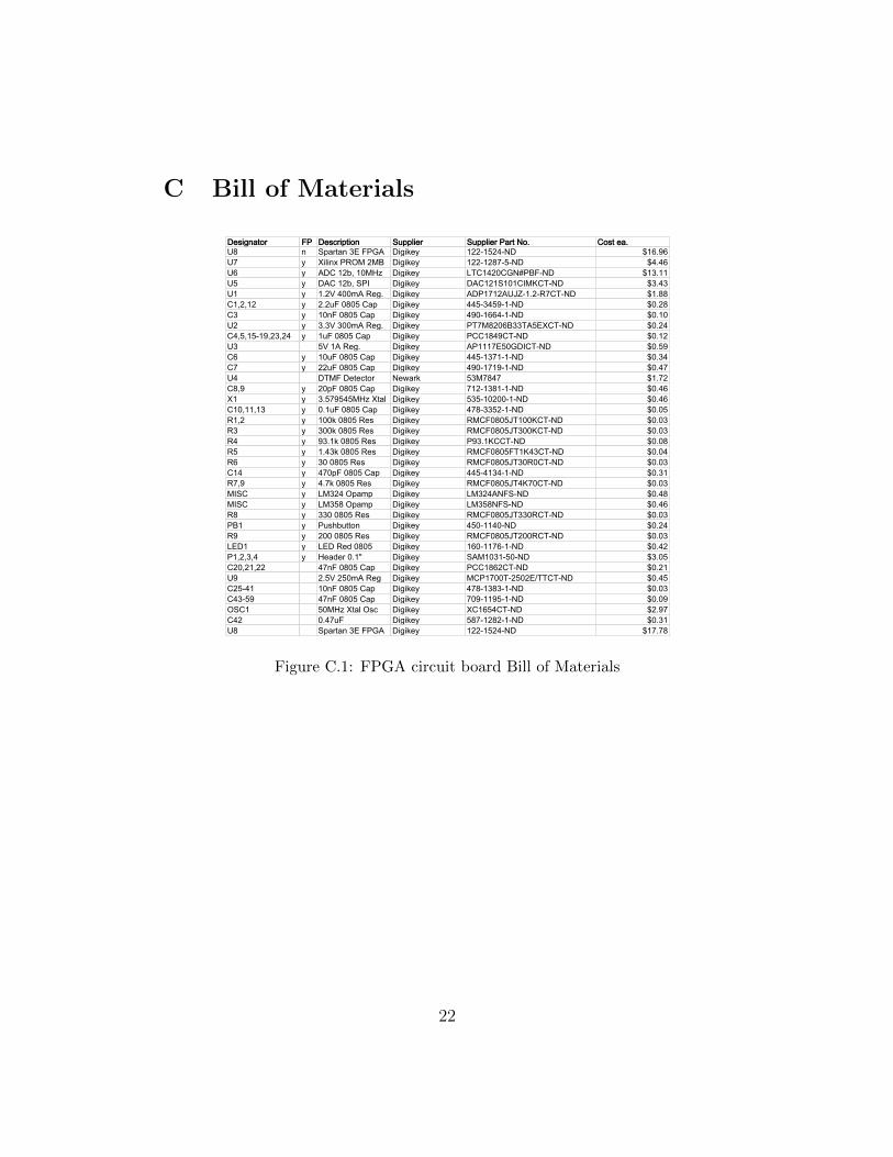
C Bill of Materials
'HVLJQDWRU )3 'HVFULSWLRQ 6XSSOLHU 6XSSOLHU�3DUW�1R� &RVW�HD�8� Q 6SDUWDQ��(�)3*$ 'LJLNH\ ���������1' ������8� \ ;LOLQ[�3520��0% 'LJLNH\ �����������1' �����8� \ $'&���E����0+] 'LJLNH\ /7&����&*1�3%)�1' ������8� \ '$&���E��63, 'LJLNH\ '$&���6���&,0.&7�1' �����8� \ ���9����P$�5HJ� 'LJLNH\ $'3����$8-=�����5�&7�1' �����&������ \ ���X)������&DS 'LJLNH\ �����������1' �����&� \ ��Q)������&DS 'LJLNH\ �����������1' �����8� \ ���9����P$�5HJ� 'LJLNH\ 37�0����%��7$�(;&7�1' �����&��������������� \ �X)������&DS 'LJLNH\ 3&&����&7�1' �����8� �9��$�5HJ� 'LJLNH\ $3����(��*',&7�1' �����&� \ ��X)������&DS 'LJLNH\ �����������1' �����&� \ ��X)������&DS 'LJLNH\ �����������1' �����8� '70)�'HWHFWRU 1HZDUN ��0���� �����&��� \ ��S)������&DS 'LJLNH\ �����������1' �����;� \ ��������0+]�;WDO 'LJLNH\ ������������1' �����&�������� \ ���X)������&DS 'LJLNH\ �����������1' �����5��� \ ���N������5HV 'LJLNH\ 50&)����-7���.&7�1' �����5� \ ���N������5HV 'LJLNH\ 50&)����-7���.&7�1' �����5� \ ����N������5HV 'LJLNH\ 3����.&&7�1' �����5� \ ����N������5HV 'LJLNH\ 50&)����)7�.��&7�1' �����5� \ ��������5HV 'LJLNH\ 50&)����-7��5�&7�1' �����&�� \ ���S)������&DS 'LJLNH\ �����������1' �����5��� \ ���N������5HV 'LJLNH\ 50&)����-7�.��&7�1' �����0,6& \ /0����2SDPS 'LJLNH\ /0���$1)6�1' �����0,6& \ /0����2SDPS 'LJLNH\ /0���1)6�1' �����5� \ ���������5HV 'LJLNH\ 50&)����-7���5&7�1' �����3%� \ 3XVKEXWWRQ 'LJLNH\ ���������1' �����5� \ ���������5HV 'LJLNH\ 50&)����-7���5&7�1' �����/('� \ /('�5HG����� 'LJLNH\ �����������1' �����3������� \ +HDGHU����� 'LJLNH\ 6$0��������1' �����&�������� ��Q)������&DS 'LJLNH\ 3&&����&7�1' �����8� ���9����P$�5HJ 'LJLNH\ 0&3����7�����(�77&7�1' �����&����� ��Q)������&DS 'LJLNH\ �����������1' �����&����� ��Q)������&DS 'LJLNH\ �����������1' �����26&� ��0+]�;WDO�2VF 'LJLNH\ ;&����&7�1' �����&�� ����X) 'LJLNH\ �����������1' �����8� 6SDUWDQ��(�)3*$ 'LJLNH\ ���������1' ������
Figure C.1: FPGA circuit board Bill of Materials
22
References
[1] M. Safadi and D. Ndzi, “Digital hardware choices for software radio (sdr)baseband implementation,” in Information and Communication Tech-
nologies, 2006. ICTTA’06. 2nd, vol. 2. IEEE, 2006, pp. 2623–2628.
[2] Xilinx Inc., “Configuration for Spartan-3A/3E FPGAs,” http://www.xilinx.com/products/design resources/config sol/s3/config s3e.htm, Jan-uary 2010.
[3] Google Inc., “Android Developer API Reference,” http://developer.android.com/reference/packages.html, March 2011.
[4] Ettus Research LLC, “Ettus Research USRP FAQ,” http://www.ettus.com/faq, May 2011.
[5] Digilent Inc., “Digilent PmodDA2 Reference Component,”http://www.digilentinc.com/Products/Detail.cfm?NavPath=2,401,487&Prod=PMOD-DA2, May 2011.
[6] P. R. Gray, Analysis and Design of Analog Integrated Circuits, 4th Edi-
tion. New York,NY, USA: John Wiley & Sons, 2001.
23
![HS DUWPHQWRI&LYLODQG(QYLURQPHQWDO(QJLQHHULQJ€¦ · 'hs duwphqwri&lylodqg(qylurqphqwdo(qjlqhhulqj ^ ,kk>k& e'/e z/e'& d^ khdd, wzdd edk& /s/>e e s/zked ed> e'/e z/e' f &}µv ]víôîðu}v](https://img.pdfslide.us/doc/110x75/5eae0abc2da2d413c14d1f2d/hs-duwphqwrilylodqgqylurqphqwdoqjlqhhulqj-hs-duwphqwrilylodqgqylurqphqwdoqjlqhhulqj.jpg)


![12 lee [Read-Only]+rzd s urfhvvruf dqs hupxwh qe lwvl q2 f \fohv 5xe\/hh =klmlh6 kl ; ldr< dqj 3ulqfhwrq$ ufklwhfwxuh/deiru0 xowlphglddqg6 hfxu lw\ 3$/06 'hsduwphqwri( ohfwulfdo( qjlqhhulqj](https://img.pdfslide.us/doc/110x75/610254c8b5d0f665f35ff556/12-lee-read-only-rzd-s-urfhvvruf-dqs-hupxwh-qe-lwvl-q2-f-fohv-5xehh-klmlh6.jpg)


![KAUSHIK DAS SHARMA CV (7) - University of Calcutta · '5 .$86+,. '$6 6+$50$ ^d/ ~h^ u d/ d ~h< u >d/^ ~/ v ] 3urihvvru 6\vwhpv (qjlqhhulqj /derudwru\ (ohfwulfdo (qjlqhhulqj](https://img.pdfslide.us/doc/110x75/5edf2ea2ad6a402d666a8838/kaushik-das-sharma-cv-7-university-of-calcutta-5-86-6-650-d-h.jpg)