Embed Size (px)
Citation preview
hsabaghianb @ kashanu.ac.irhsabaghianb @ kashanu.ac.ir MicroprocessorsMicroprocessors 4-4-11
An Introduction to
8051 Microcontroller
(Hardware Specification)
Lec note 4
hsabaghianb @ kashanu.ac.irhsabaghianb @ kashanu.ac.ir MicroprocessorsMicroprocessors 4-4-22
Intruduction
Microprocessor = CPU on a single chip. ALU + registers + control +…
Micro-computer = small computeruP + I/O + memory + peripheral + …
Microcontroller (uC) u-Computer on a single chip of silicon
hsabaghianb @ kashanu.ac.irhsabaghianb @ kashanu.ac.ir MicroprocessorsMicroprocessors 4-4-33
uP vs. uC
A uPuP single-chip contained only CPU bus is availablebus is available RAM capacity, num of port is selectable RAM is larger than ROM (usually)
A uC single-chip contained CPU, RAM, ROM, Prepherals, I/O
port Communicate by port internal hardware is fixed ROM is larger than RAM (usually)
hsabaghianb @ kashanu.ac.irhsabaghianb @ kashanu.ac.ir MicroprocessorsMicroprocessors 4-4-44
uC base system
Small power consumptionSingle chip, small board Implementation is easyLow cost
Can be used as Reconfigurable HardwareuC can reprogram on the fly(ISP)
hsabaghianb @ kashanu.ac.irhsabaghianb @ kashanu.ac.ir MicroprocessorsMicroprocessors 4-4-55
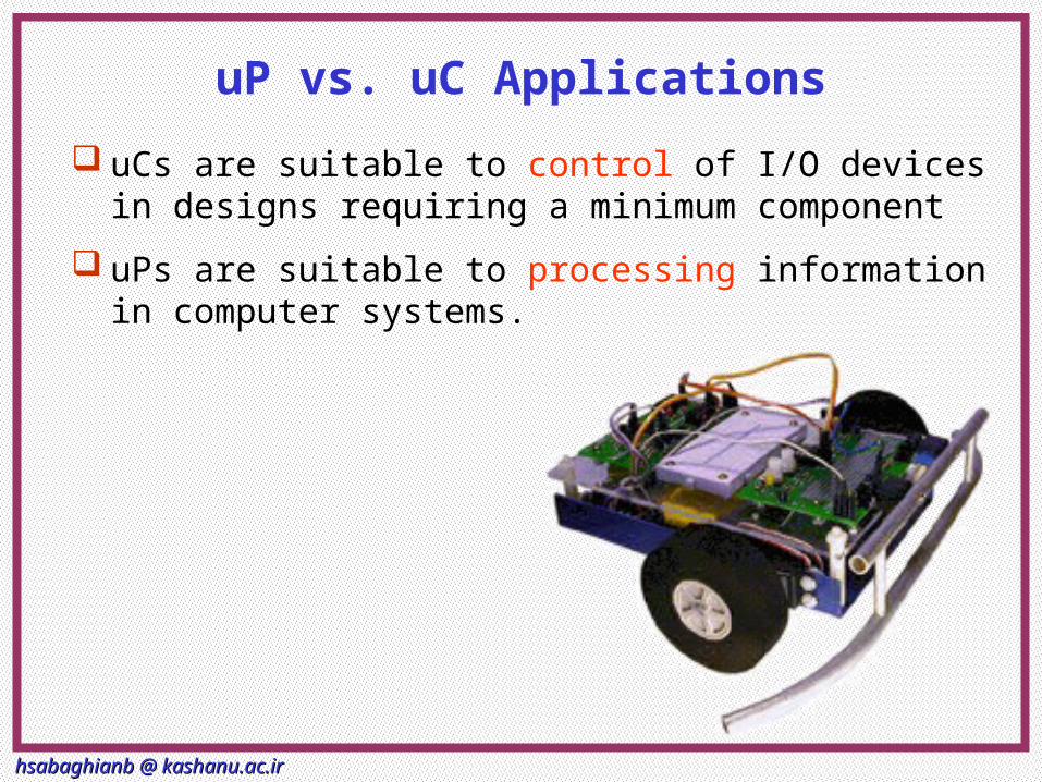
uCs are suitable to control of I/O devices in designs requiring a minimum component
uPs are suitable to processing information in computer systems.
uP vs. uC Applications
hsabaghianb @ kashanu.ac.irhsabaghianb @ kashanu.ac.ir MicroprocessorsMicroprocessors 4-4-66
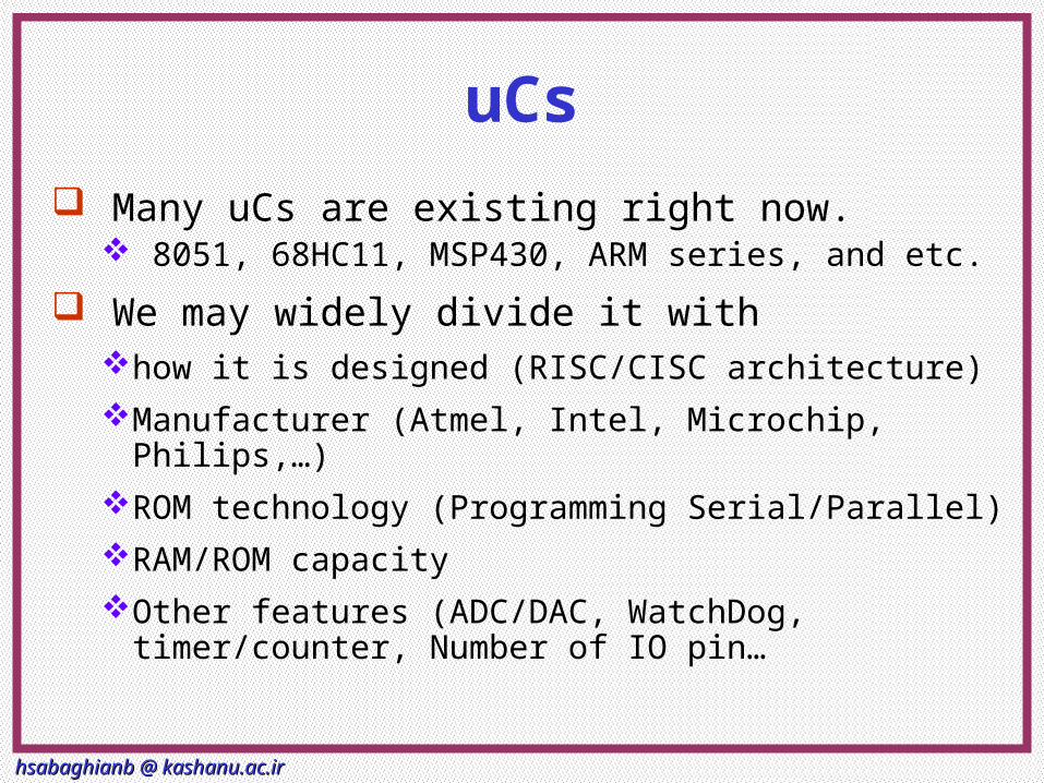
uCs
Many uCs are existing right now. 8051, 68HC11, MSP430, ARM series, and etc.
We may widely divide it with how it is designed (RISC/CISC architecture)Manufacturer (Atmel, Intel, Microchip, Philips,…)ROM technology (Programming Serial/Parallel)RAM/ROM capacityOther features (ADC/DAC, WatchDog,
timer/counter, Number of IO pin…
hsabaghianb @ kashanu.ac.irhsabaghianb @ kashanu.ac.ir MicroprocessorsMicroprocessors 4-4-77
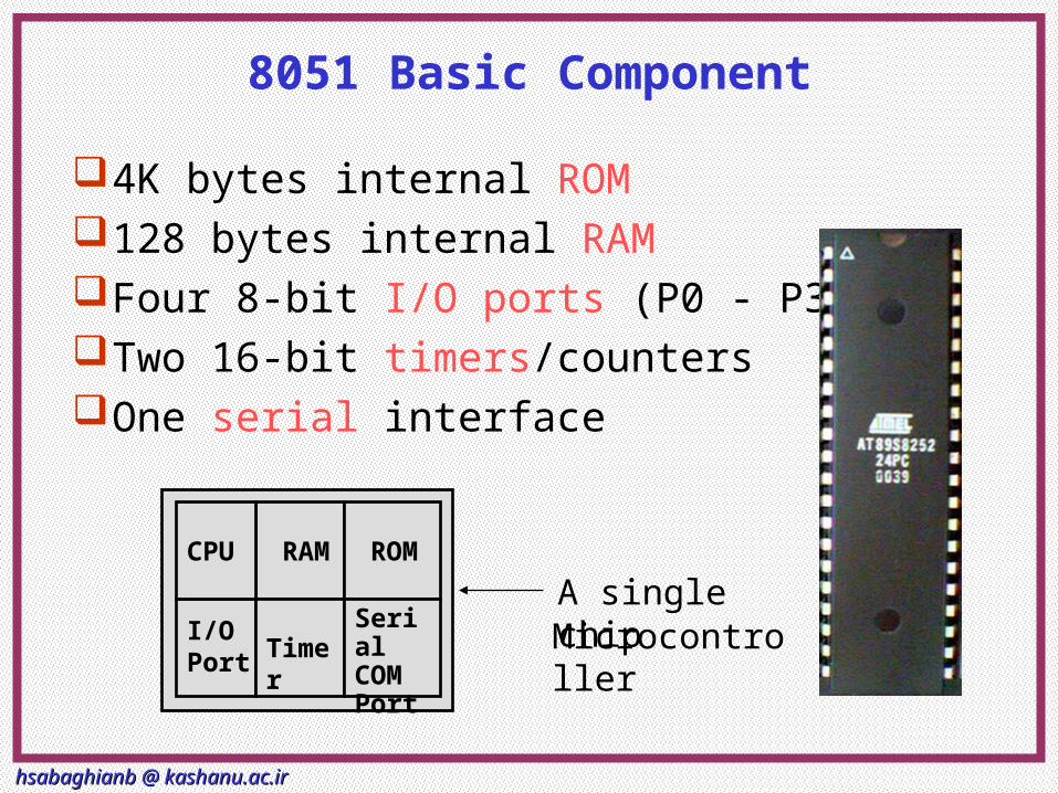
8051 Basic Component
4K bytes internal ROM128 bytes internal RAMFour 8-bit I/O ports (P0 - P3).Two 16-bit timers/countersOne serial interface
RAM
I/O Port Timer
Serial COM Port
Microcontroller
CPU
A single chip ROM
hsabaghianb @ kashanu.ac.irhsabaghianb @ kashanu.ac.ir MicroprocessorsMicroprocessors 4-4-88
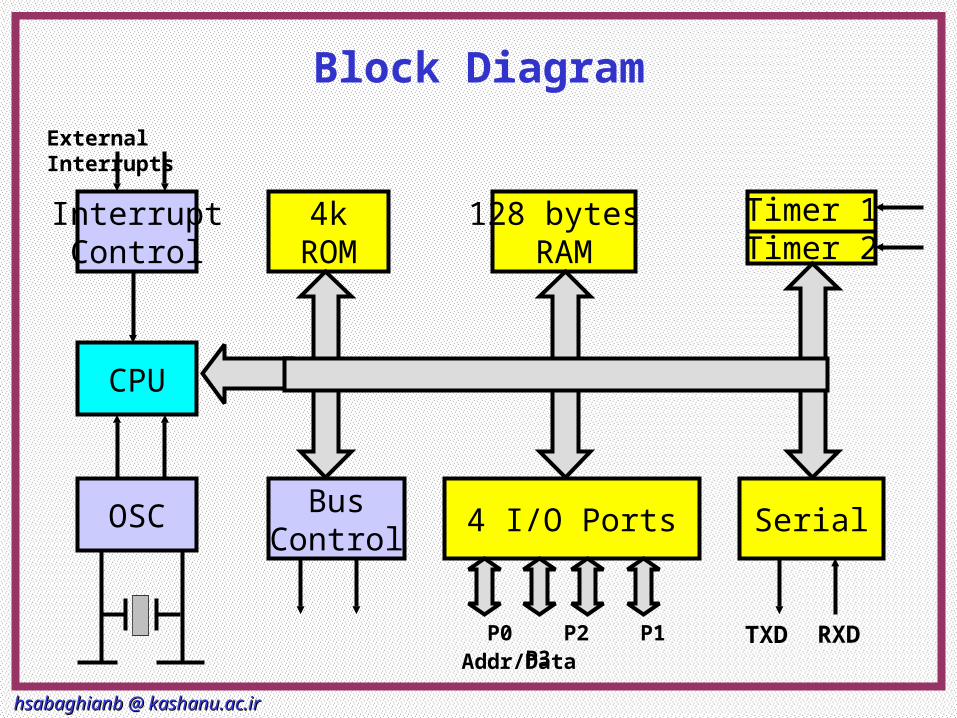
Block Diagram
CPU
InterruptControl
OSC BusControl
4kROM
Timer 1Timer 2
Serial
128 bytes RAM
4 I/O Ports
TXD RXD
External Interrupts
P0 P2 P1 P3Addr/Data
hsabaghianb @ kashanu.ac.irhsabaghianb @ kashanu.ac.ir MicroprocessorsMicroprocessors 4-4-99
Other 8051 featurs
only 1 On chip oscillator (external crystal)
6 interrupt sources (2 external , 3 internal, Reset)
64K external code (program) memory(only
read)PSEN
64K external data memory(can be read and write)
by RD,WR
Code memory is selectable by EA (internal or
external)
We may have External memory as data and code
hsabaghianb @ kashanu.ac.irhsabaghianb @ kashanu.ac.ir MicroprocessorsMicroprocessors 4-4-1010
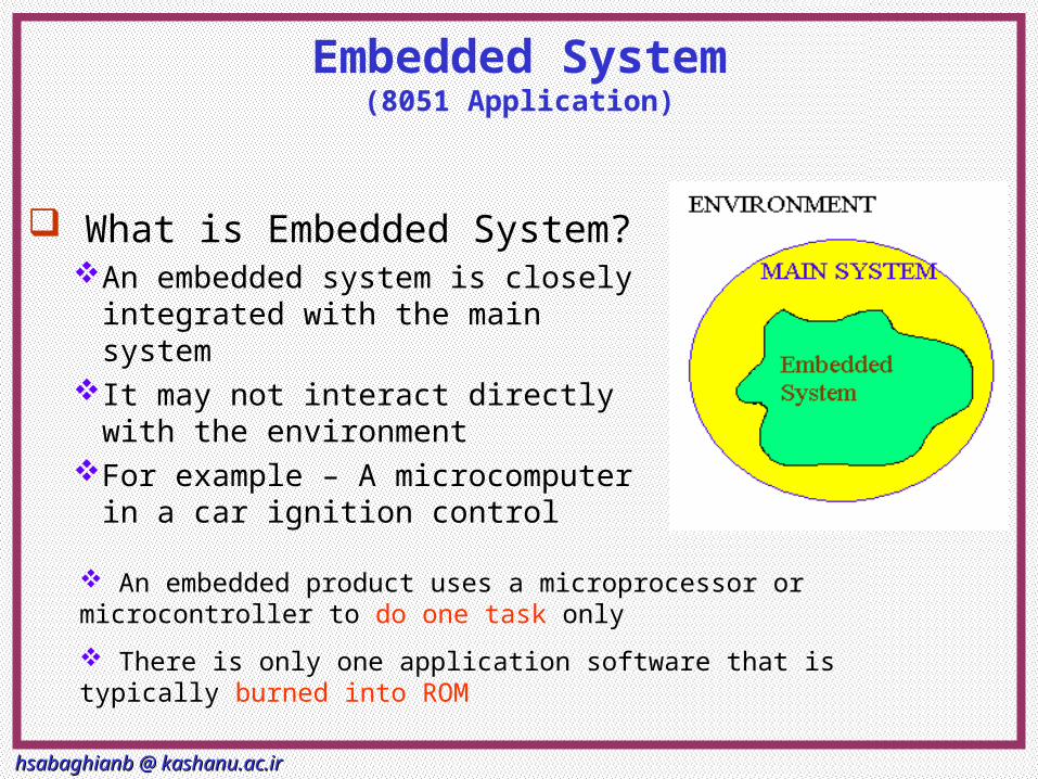
Embedded System(8051 Application)
What is Embedded System?An embedded system is closely
integrated with the main systemIt may not interact directly with
the environmentFor example – A microcomputer
in a car ignition control
An embedded product uses a microprocessor or microcontroller to do one task only
There is only one application software that is typically burned into ROM
hsabaghianb @ kashanu.ac.irhsabaghianb @ kashanu.ac.ir MicroprocessorsMicroprocessors 4-4-1111
Examples of Embedded Systems
KeyboardPrintervideo game playerMP3 music playersEmbedded memories to keep
configuration informationMobile phone unitsDomestic (home) appliancesData switchesAutomotive controls
hsabaghianb @ kashanu.ac.irhsabaghianb @ kashanu.ac.ir MicroprocessorsMicroprocessors 4-4-1212
Choosing a Microcontroller
meeting the computing needs of the task efficiently and cost effectivelyspeed, the amount of ROM and RAM, the number of
I/O ports and timers, size, packaging, power consumption
easy to upgradecost per unit
availability of software development toolsassemblers, debuggers, C compilers, emulator,
simulator, technical support
wide availability and reliable sources of the microcontrollers
hsabaghianb @ kashanu.ac.irhsabaghianb @ kashanu.ac.ir MicroprocessorsMicroprocessors 4-4-1313
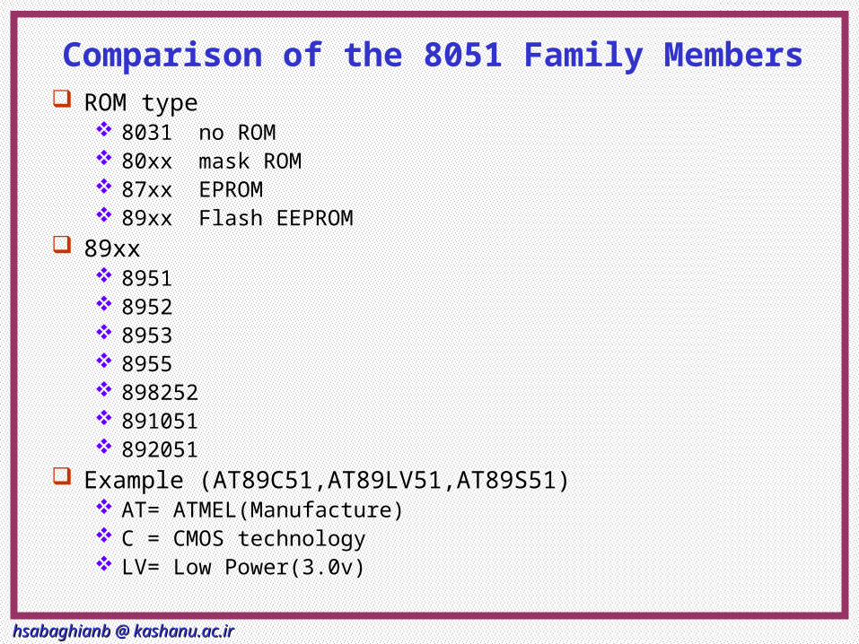
Comparison of the 8051 Family Members ROM type
8031 no ROM 80xx mask ROM 87xx EPROM 89xx Flash EEPROM
89xx 8951 8952 8953 8955 898252 891051 892051
Example (AT89C51,AT89LV51,AT89S51) AT= ATMEL(Manufacture) C = CMOS technology LV= Low Power(3.0v)
hsabaghianb @ kashanu.ac.irhsabaghianb @ kashanu.ac.ir MicroprocessorsMicroprocessors 4-4-1414
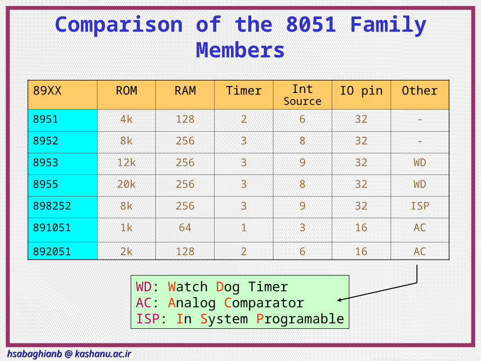
Comparison of the 8051 Family Members
89XX ROM RAM Timer Int Source
IO pin Other
8951 4k 128 2 6 32 -
8952 8k 256 3 8 32 -
8953 12k 256 3 9 32 WD
8955 20k 256 3 8 32 WD
898252 8k 256 3 9 32 ISP
891051 1k 64 1 3 16 AC
892051 2k 128 2 6 16 AC
WD: Watch Dog TimerAC: Analog ComparatorISP: In System Programable
hsabaghianb @ kashanu.ac.irhsabaghianb @ kashanu.ac.ir MicroprocessorsMicroprocessors 4-4-1515
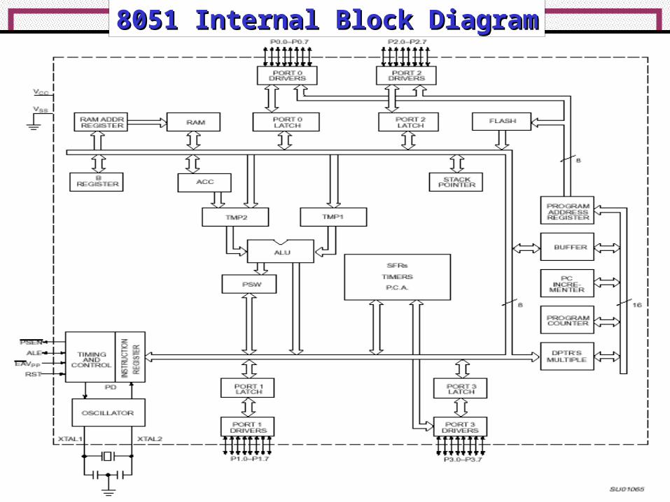
8051 Internal Block Diagram8051 Internal Block Diagram
hsabaghianb @ kashanu.ac.irhsabaghianb @ kashanu.ac.ir MicroprocessorsMicroprocessors 4-4-1616
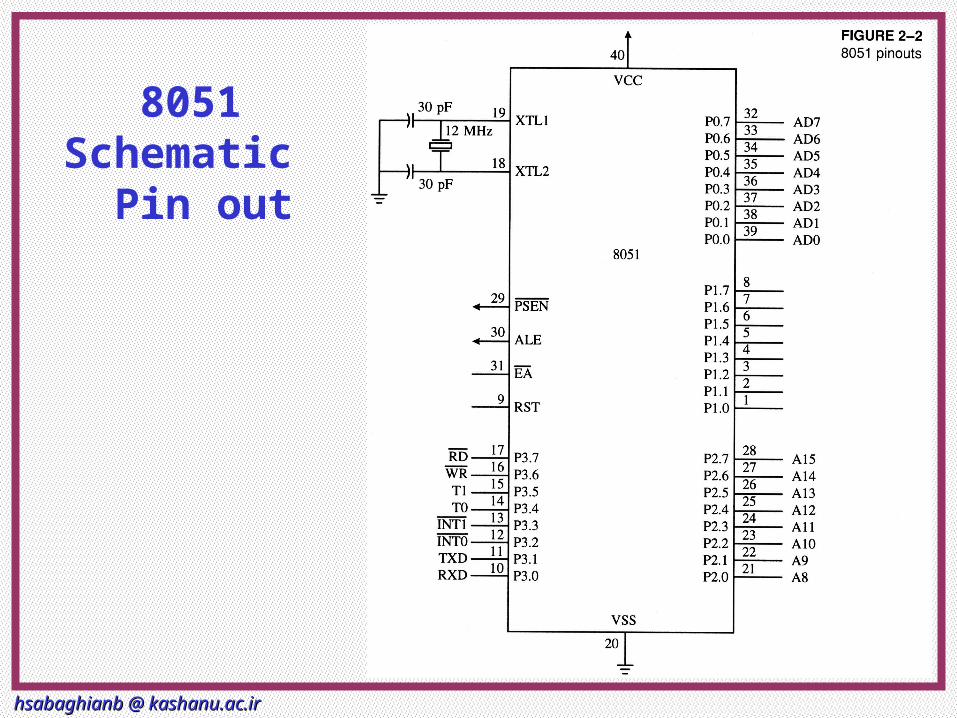
8051 Schematic
Pin out
hsabaghianb @ kashanu.ac.irhsabaghianb @ kashanu.ac.ir MicroprocessorsMicroprocessors 4-4-1717
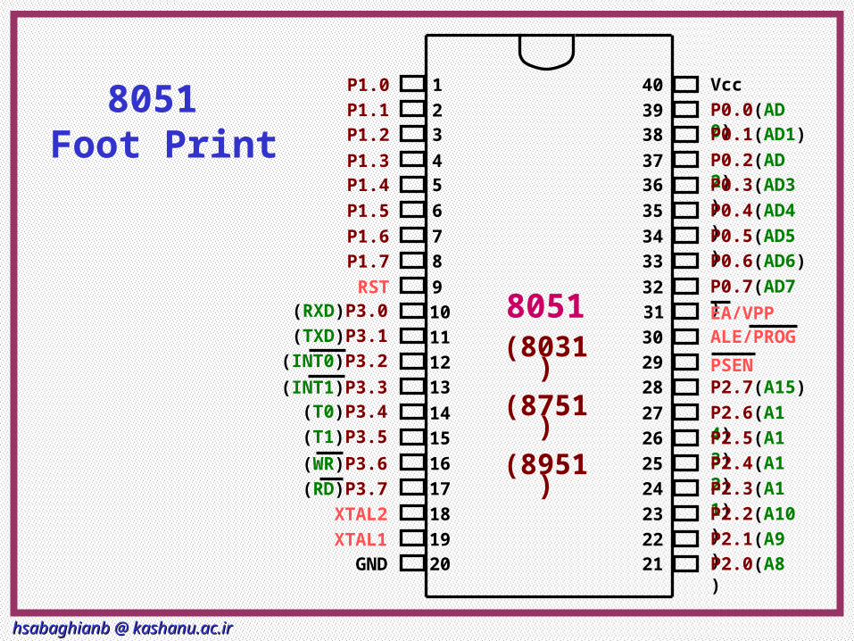
8051 Foot Print
1
23
45
6
7
8
9
10
11
1213
14
15
16
17
18
1920
40
3938
3736
35
34
33
32
31
30
2928
27
26
25
24
23
2221
P1.0
P1.1P1.2
P1.3P1.4
P1.5
P1.6
P1.7
RST(RXD)P3.0
(TXD)P3.1
(T0)P3.4
(T1)P3.5
XTAL2
XTAL1GND
(INT0)P3.2
(INT1)P3.3
(RD)P3.7
(WR)P3.6
Vcc
P0.0(AD0)P0.1(AD1)
P0.2(AD2)P0.3(AD3)
P0.4(AD4)
P0.5(AD5)
P0.6(AD6)
P0.7(AD7)
EA/VPPALE/PROG
PSENP2.7(A15)
P2.6(A14)P2.5(A13)P2.4(A12)P2.3(A11)P2.2(A10)
P2.1(A9)
P2.0(A8)
8051(8031)(8751)(8951)
hsabaghianb @ kashanu.ac.irhsabaghianb @ kashanu.ac.ir MicroprocessorsMicroprocessors 4-4-1818
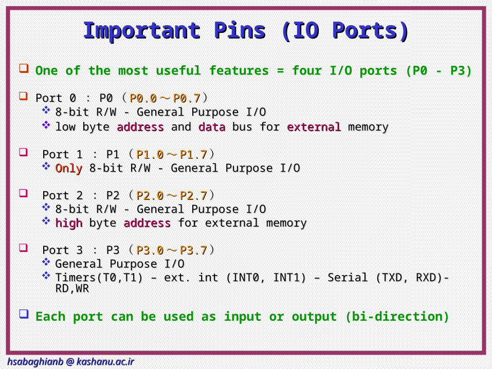
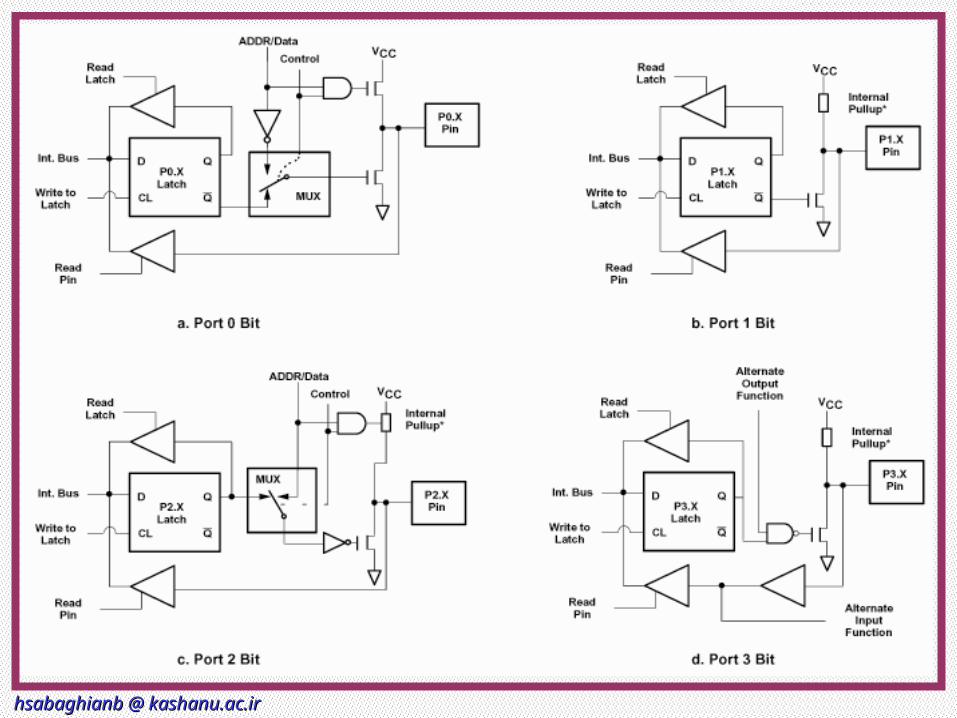
Important Pins (IO Ports)Important Pins (IO Ports)
One of the most useful features = four I/O ports (P0 - P3)
Port 0 Port 0 :: P0P0 (( P0.0P0.0 ~~ P0.7P0.7 )) 8-bit R/W - General Purpose I/O8-bit R/W - General Purpose I/O low byte low byte addressaddress and and datadata bus for bus for externalexternal memory memory
Port 1 Port 1 :: P1P1 (( P1.0P1.0 ~~ P1.7P1.7 )) OnlyOnly 8-bit R/W - General Purpose I/O 8-bit R/W - General Purpose I/O
Port 2 Port 2 :: P2P2 (( P2.0P2.0 ~~ P2.7P2.7 )) 8-bit R/W - General Purpose I/O8-bit R/W - General Purpose I/O highhigh byte byte addressaddress for external memory for external memory
Port 3 Port 3 :: P3P3 (( P3.0P3.0 ~~ P3.7P3.7 )) General Purpose I/OGeneral Purpose I/O Timers(T0,T1) – ext. int (INT0, INT1) – Serial (TXD, RXD)- RD,WRTimers(T0,T1) – ext. int (INT0, INT1) – Serial (TXD, RXD)- RD,WR
Each port can be used as input or output (bi-direction)
hsabaghianb @ kashanu.ac.irhsabaghianb @ kashanu.ac.ir MicroprocessorsMicroprocessors 4-4-1919
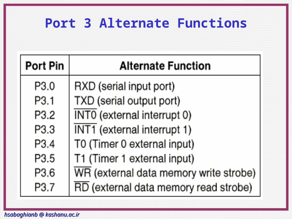
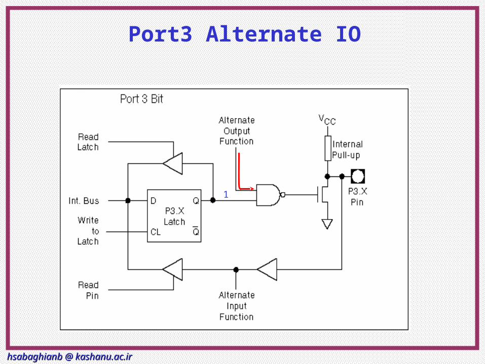
Port 3 Alternate Functions
hsabaghianb @ kashanu.ac.irhsabaghianb @ kashanu.ac.ir MicroprocessorsMicroprocessors 4-4-2020
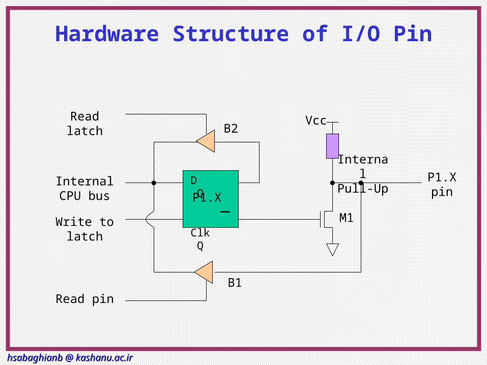
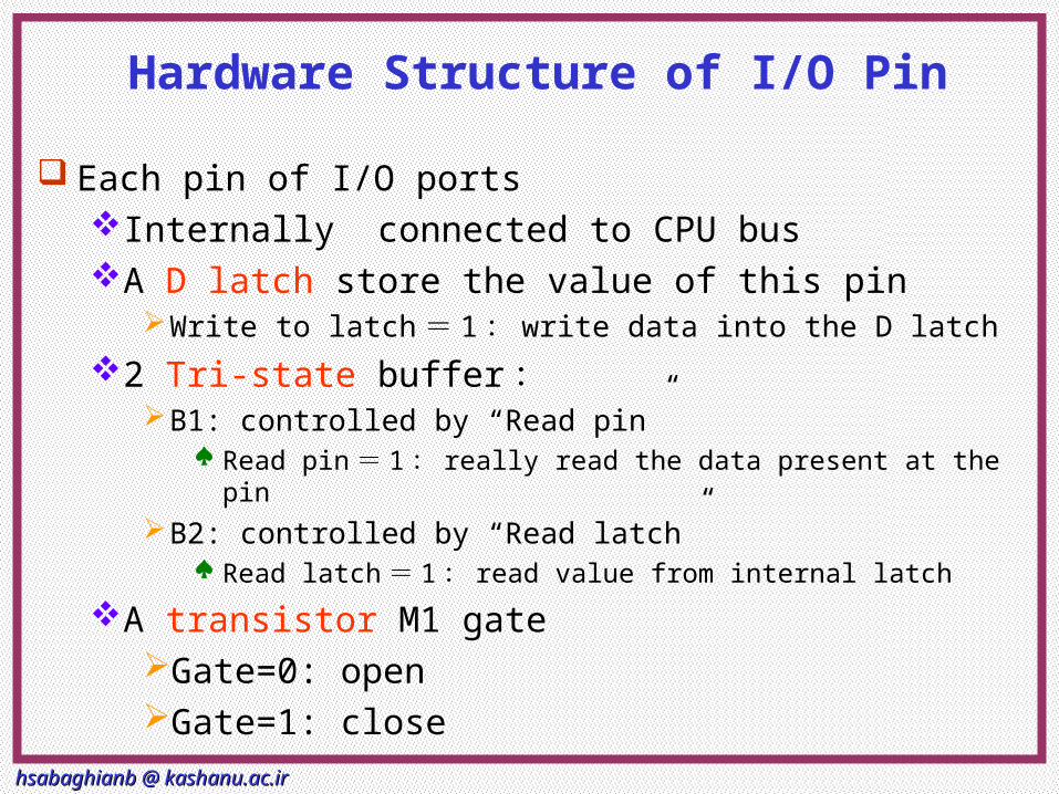
Hardware Structure of I/O Pin
D Q
Clk Q
Vcc
InternalPull-Up
Read latch
Read pin
Write to latch
Internal CPU bus
M1
P1.X pinP1.X
B1
B2
hsabaghianb @ kashanu.ac.irhsabaghianb @ kashanu.ac.ir MicroprocessorsMicroprocessors 4-4-2121
Hardware Structure of I/O Pin
Each pin of I/O portsInternally connected to CPU busA D latch store the value of this pin
Write to latch = 1 : write data into the D latch
2 Tri-state buffer :B1: controlled by “Read pin”
Read pin = 1 : really read the data present at the pinB2: controlled by “Read latch”
Read latch = 1 : read value from internal latch
A transistor M1 gateGate=0: openGate=1: close
hsabaghianb @ kashanu.ac.irhsabaghianb @ kashanu.ac.ir MicroprocessorsMicroprocessors 4-4-2222
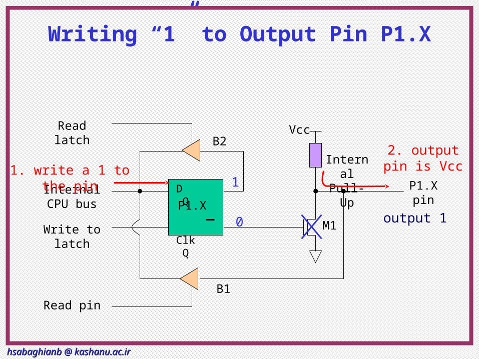
Writing “1” to Output Pin P1.X
D Q
Clk Q
Vcc
InternalPull-Up
Read latch
Read pin
Write to latch
Internal CPU bus
M1
P1.X pinP1.X
2. output pin is Vcc1. write a 1 to the pin
1
0 output 1
B1
B2
hsabaghianb @ kashanu.ac.irhsabaghianb @ kashanu.ac.ir MicroprocessorsMicroprocessors 4-4-2323
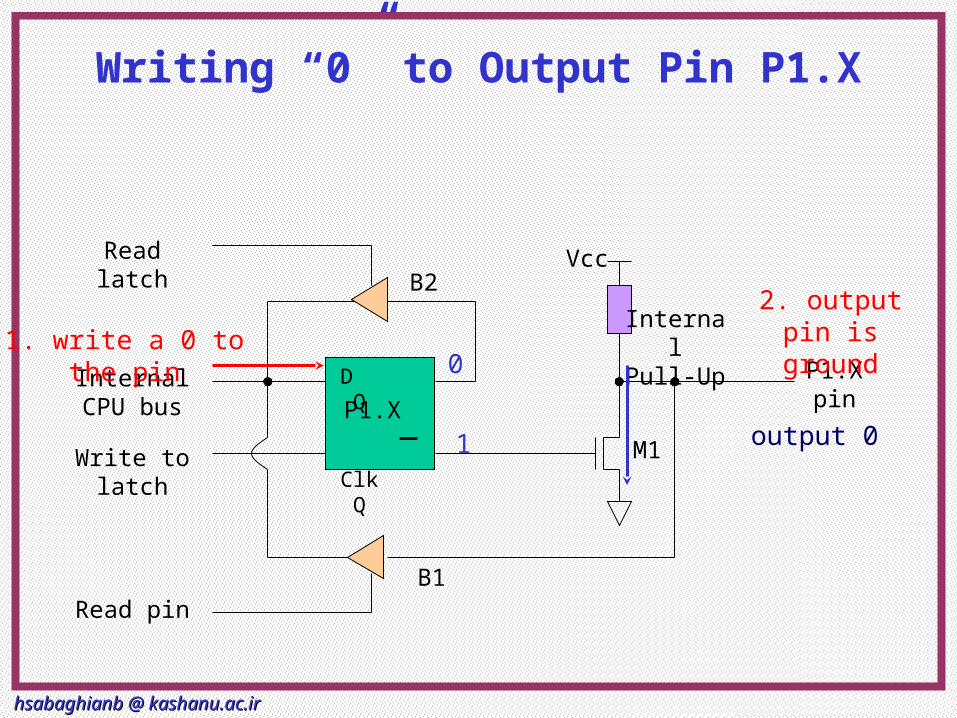
Writing “0” to Output Pin P1.X
D Q
Clk Q
Vcc
InternalPull-Up
Read latch
Read pin
Write to latch
Internal CPU bus
M1
P1.X pinP1.X
2. output pin is ground1. write a 0 to the pin
0
1 output 0
B1
B2
hsabaghianb @ kashanu.ac.irhsabaghianb @ kashanu.ac.ir MicroprocessorsMicroprocessors 4-4-2424
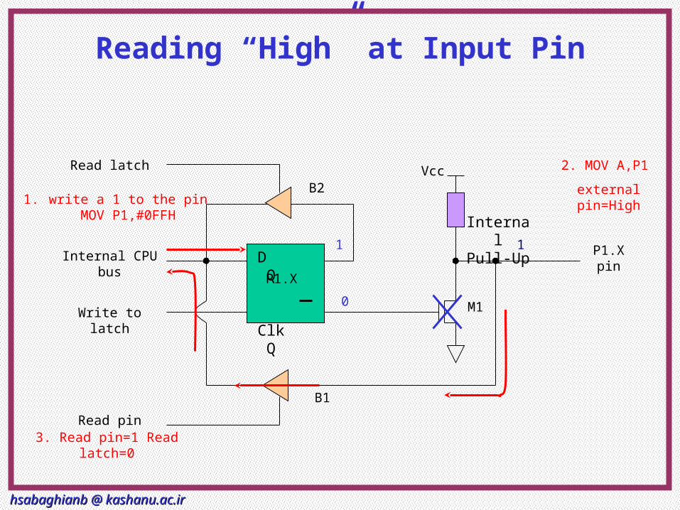
Reading “High” at Input Pin
D Q
Clk Q
Vcc
InternalPull-Up
Read latch
Read pin
Write to latch
Internal CPU bus
M1
P1.X pin
P1.X
2. MOV A,P1
external pin=High1. write a 1 to the pin MOV
P1,#0FFH
1
0
3. Read pin=1 Read latch=0
1
B1
B2
hsabaghianb @ kashanu.ac.irhsabaghianb @ kashanu.ac.ir MicroprocessorsMicroprocessors 4-4-2525
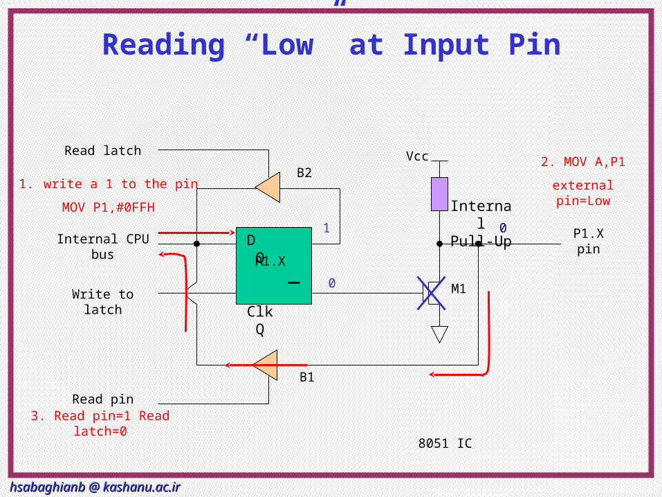
Reading “Low” at Input Pin
D Q
Clk Q
Vcc
InternalPull-Up
Read latch
Read pin
Write to latch
Internal CPU bus
M1
P1.X pin
P1.X
8051 IC
2. MOV A,P1
external pin=Low1. write a 1 to the pin
MOV P1,#0FFH
1
0
3. Read pin=1 Read latch=0
0
B1
B2
hsabaghianb @ kashanu.ac.irhsabaghianb @ kashanu.ac.ir MicroprocessorsMicroprocessors 4-4-2626
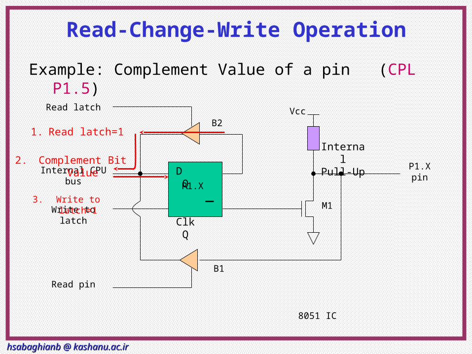
Read-Change-Write Operation
D Q
Clk Q
Vcc
InternalPull-Up
Read latch
Read pin
Write to latch
Internal CPU bus
M1
P1.X pin
P1.X
8051 IC
1. Read latch=1
3. Write to latch=1
B1
B2
Example: Complement Value of a pin (CPL P1.5)
2. Complement Bit Value
hsabaghianb @ kashanu.ac.irhsabaghianb @ kashanu.ac.ir MicroprocessorsMicroprocessors 4-4-2727
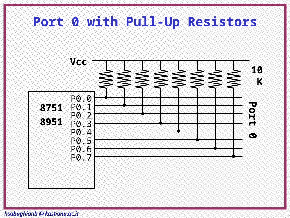
Port 0 with Pull-Up Resistors
P0.0P0.1P0.2P0.3P0.4P0.5P0.6P0.7
8751
8951
Vcc10 K
Port 0
hsabaghianb @ kashanu.ac.irhsabaghianb @ kashanu.ac.ir MicroprocessorsMicroprocessors 4-4-2828
Port3 Alternate IO
1
hsabaghianb @ kashanu.ac.irhsabaghianb @ kashanu.ac.ir MicroprocessorsMicroprocessors 4-4-2929
hsabaghianb @ kashanu.ac.irhsabaghianb @ kashanu.ac.ir MicroprocessorsMicroprocessors 4-4-3030
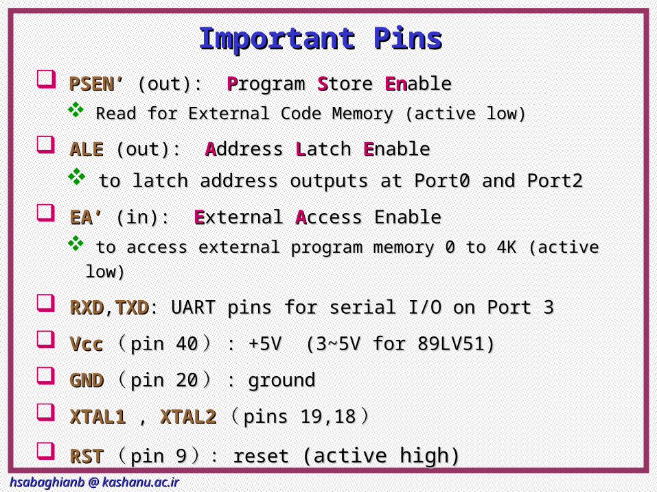
Important Pins Important Pins PSEN’PSEN’ (out): (out): PProgram rogram SStore tore EnEnable able
Read for External Code Memory (active low)Read for External Code Memory (active low)
ALEALE (out): (out): AAddress ddress LLatch atch EEnable nable
to latch address outputs at Port0 and Port2to latch address outputs at Port0 and Port2
EA’EA’ (in): (in): EExternal xternal AAccess Enableccess Enable
to access external program memory 0 to 4K (active low) to access external program memory 0 to 4K (active low)
RXDRXD,,TXDTXD: UART pins for serial I/O on Port 3: UART pins for serial I/O on Port 3
VccVcc (( pin 40pin 40 )) : +5V (3~5V for 89LV51): +5V (3~5V for 89LV51)
GNDGND (( pin 20pin 20 )) : ground: ground
XTAL1XTAL1 , , XTAL2XTAL2 (( pins 19,18pins 19,18 ))
RSTRST (( pin 9pin 9 ):): reset reset (active high) (active high)
hsabaghianb @ kashanu.ac.irhsabaghianb @ kashanu.ac.ir MicroprocessorsMicroprocessors 4-4-3131
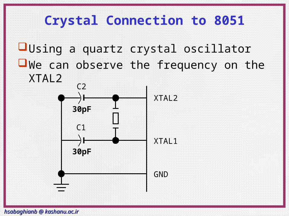
Crystal Connection to 8051
Using a quartz crystal oscillatorWe can observe the frequency on the
XTAL2C2
30pF
C1
30pF
XTAL2
XTAL1
GND
hsabaghianb @ kashanu.ac.irhsabaghianb @ kashanu.ac.ir MicroprocessorsMicroprocessors 4-4-3232
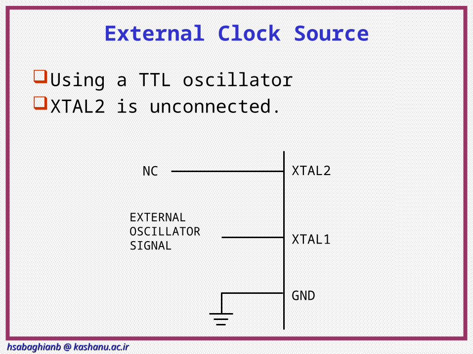
External Clock Source
Using a TTL oscillatorXTAL2 is unconnected.
NC
EXTERNALOSCILLATORSIGNAL
XTAL2
XTAL1
GND
hsabaghianb @ kashanu.ac.irhsabaghianb @ kashanu.ac.ir MicroprocessorsMicroprocessors 4-4-3333
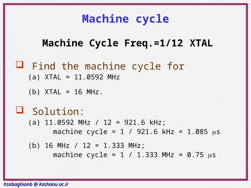
Machine cycle
Machine Cycle Freq.=1/12 XTAL
Find the machine cycle for(a) XTAL = 11.0592 MHz
(b) XTAL = 16 MHz.
Solution:(a) 11.0592 MHz / 12 = 921.6 kHz; machine cycle = 1 / 921.6 kHz = 1.085 s
(b) 16 MHz / 12 = 1.333 MHz; machine cycle = 1 / 1.333 MHz = 0.75 s
hsabaghianb @ kashanu.ac.irhsabaghianb @ kashanu.ac.ir MicroprocessorsMicroprocessors 4-4-3434
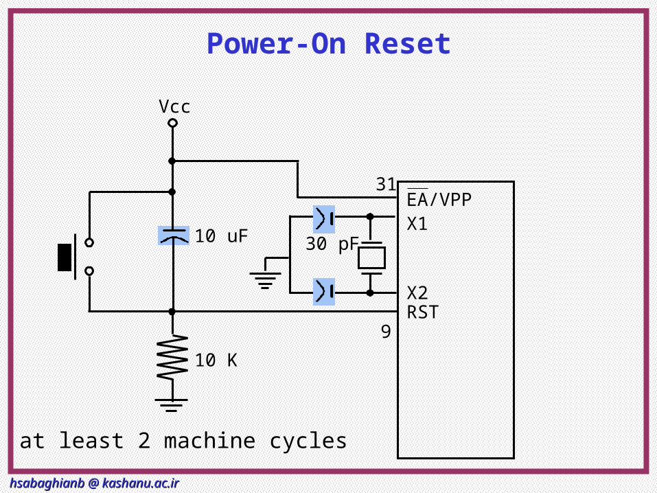
Power-On Reset
EA/VPPX1
X2RST
Vcc
10 uF
10 K
30 pF
9
31
at least 2 machine cycles
hsabaghianb @ kashanu.ac.irhsabaghianb @ kashanu.ac.ir MicroprocessorsMicroprocessors 4-4-3535
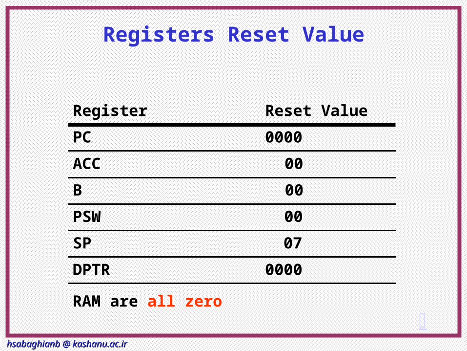
Registers Reset Value
0000DPTR
07SP
00PSW
00B
00ACC
0000PC
Reset ValueRegister
RAM are all zero
hsabaghianb @ kashanu.ac.irhsabaghianb @ kashanu.ac.ir MicroprocessorsMicroprocessors 4-4-3636
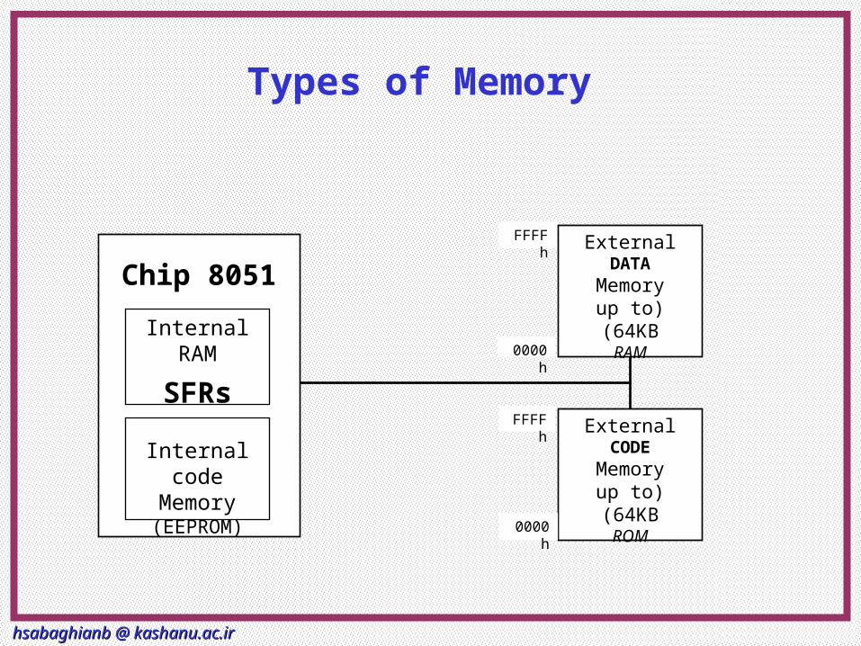
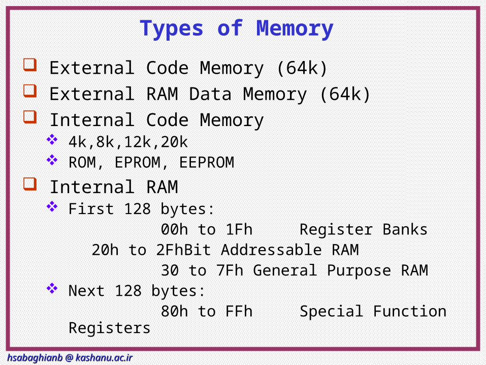
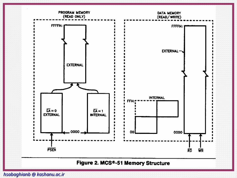
Types of Memory
ExternalDATA
Memory)up to 64KB(
RAM
ExternalCODE
Memory)up to 64KB(
ROM
8051 Chip
0000h
FFFFh
FFFFh
Internal RAM
SFRs
Internal code Memory
(EEPROM)0000h
hsabaghianb @ kashanu.ac.irhsabaghianb @ kashanu.ac.ir MicroprocessorsMicroprocessors 4-4-3737
Types of Memory
External Code Memory (64k) External RAM Data Memory (64k) Internal Code Memory
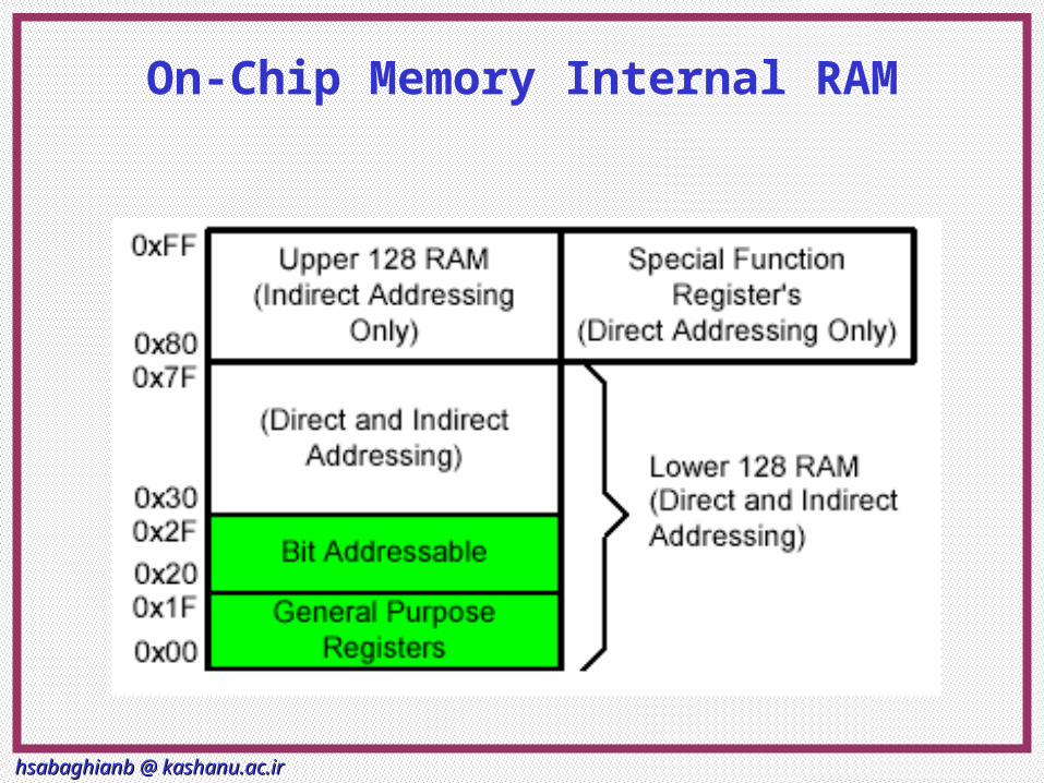
4k,8k,12k,20k ROM, EPROM, EEPROM
Internal RAM First 128 bytes:
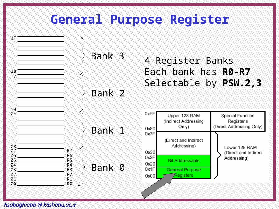
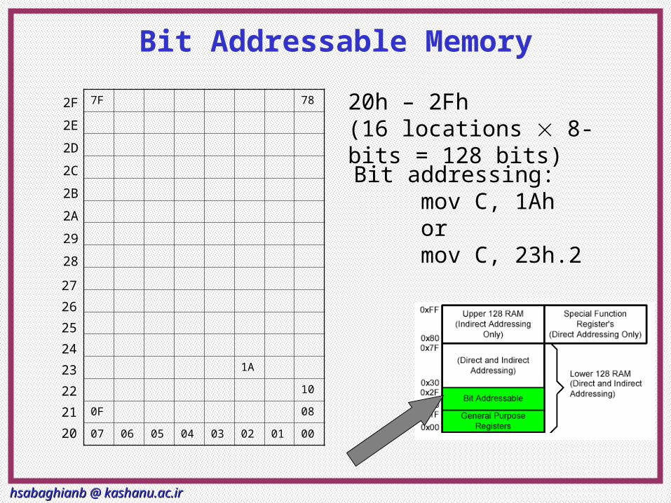
00h to 1Fh Register Banks20h to 2Fh Bit Addressable RAM
30 to 7Fh General Purpose RAM Next 128 bytes:
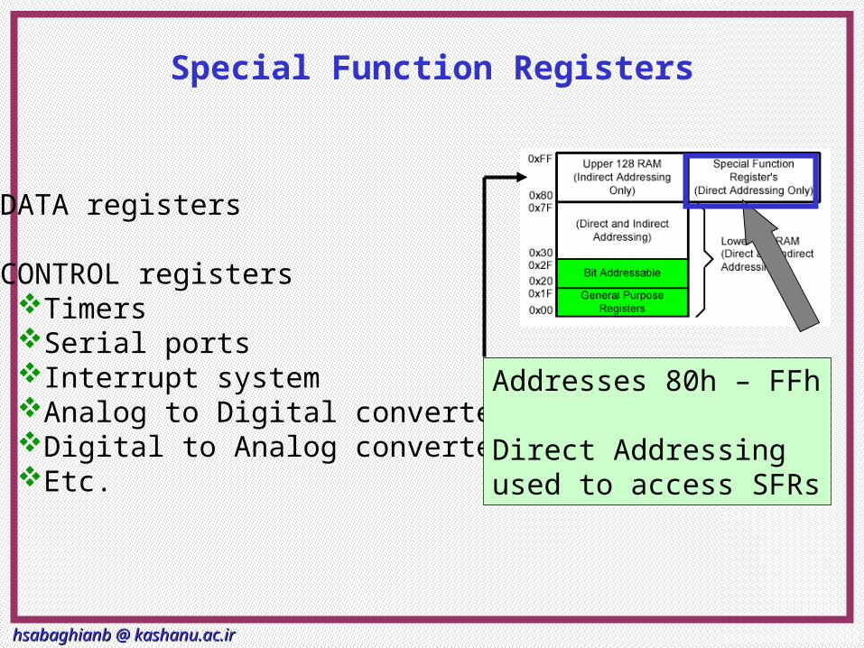
80h to FFh Special Function Registers
hsabaghianb @ kashanu.ac.irhsabaghianb @ kashanu.ac.ir MicroprocessorsMicroprocessors 4-4-3838
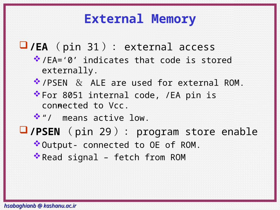
External Memory
/EA ( pin 31 ): external access /EA=‘0’ indicates that code is stored externally. /PSEN & ALE are used for external ROM.For 8051 internal code, /EA pin is connected to
Vcc.“/” means active low.
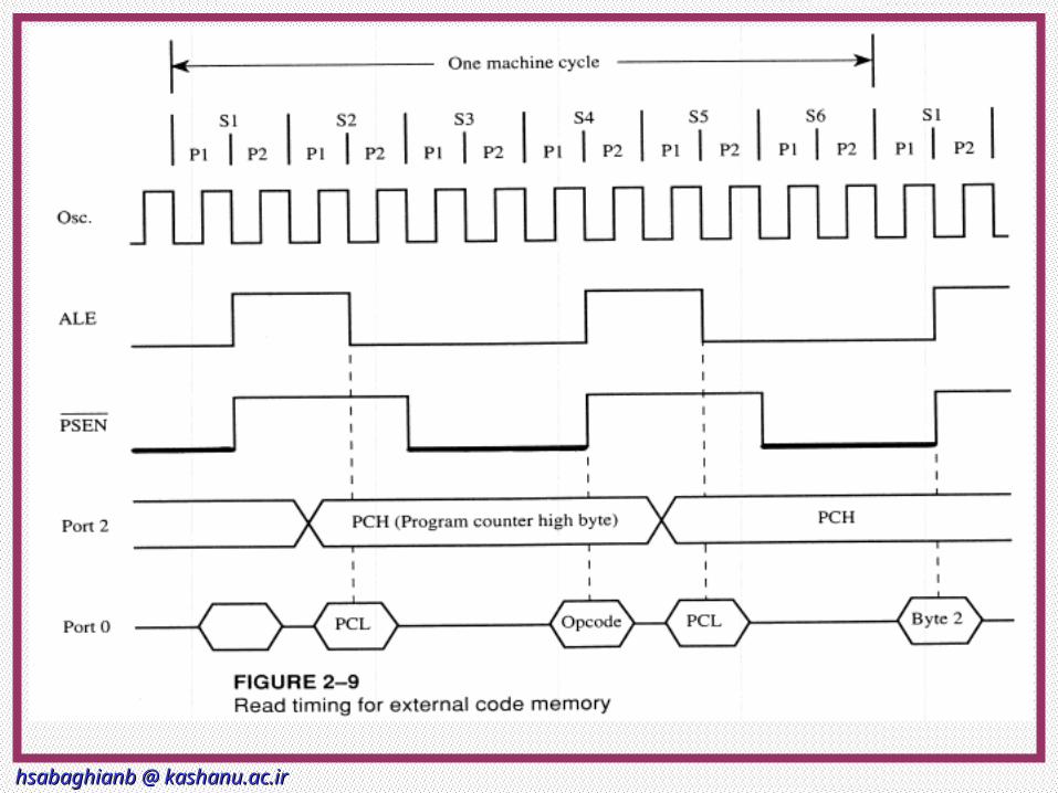
/PSEN ( pin 29 ): program store enableOutput- connected to OE of ROM.Read signal – fetch from ROM
hsabaghianb @ kashanu.ac.irhsabaghianb @ kashanu.ac.ir MicroprocessorsMicroprocessors 4-4-3939
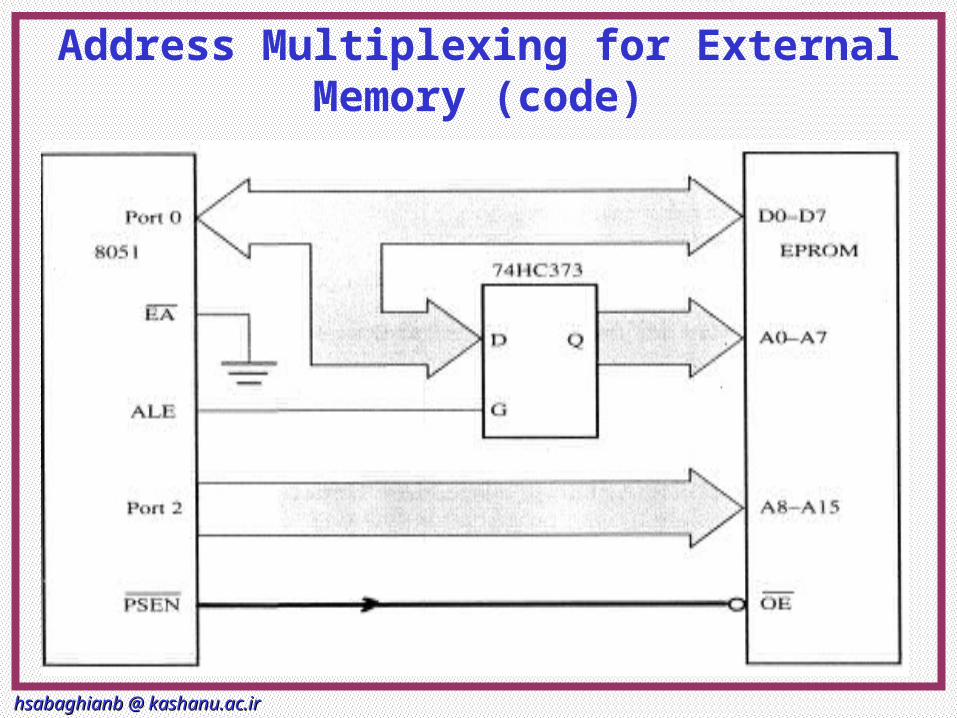
External Memory
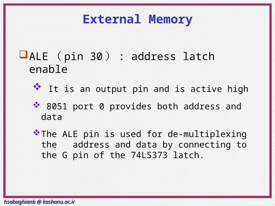
ALE ( pin 30 ) : address latch enable
It is an output pin and is active high
8051 port 0 provides both address and data
The ALE pin is used for de-multiplexing the address and data by connecting to the G pin of the 74LS373 latch.
hsabaghianb @ kashanu.ac.irhsabaghianb @ kashanu.ac.ir MicroprocessorsMicroprocessors 4-4-4040
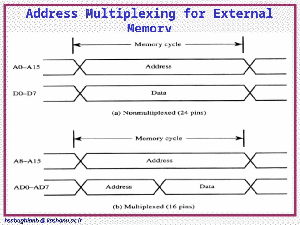
Address Multiplexing for External Memory
hsabaghianb @ kashanu.ac.irhsabaghianb @ kashanu.ac.ir MicroprocessorsMicroprocessors 4-4-4141
Address Multiplexing for External Memory (code)
hsabaghianb @ kashanu.ac.irhsabaghianb @ kashanu.ac.ir MicroprocessorsMicroprocessors 4-4-4242
hsabaghianb @ kashanu.ac.irhsabaghianb @ kashanu.ac.ir MicroprocessorsMicroprocessors 4-4-4343
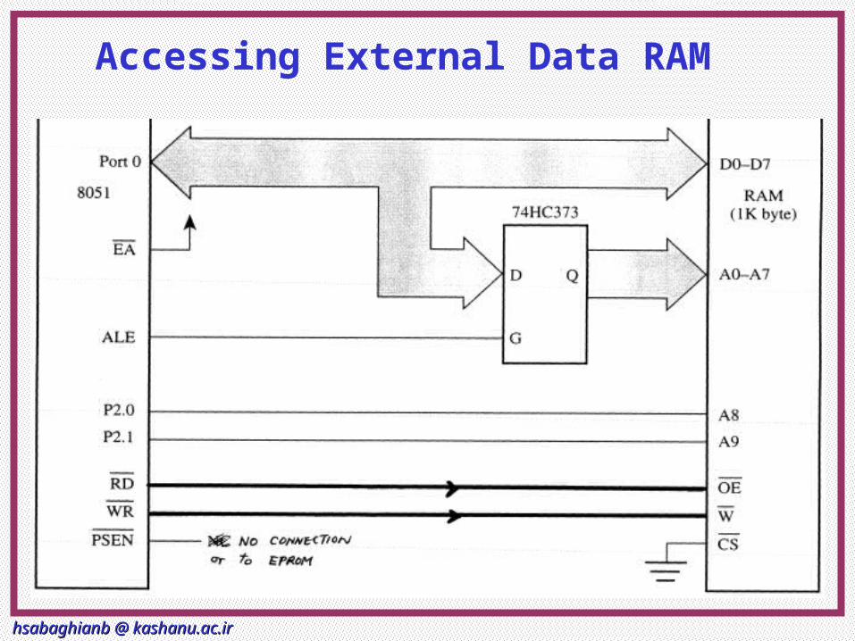
Accessing External Data RAM
hsabaghianb @ kashanu.ac.irhsabaghianb @ kashanu.ac.ir MicroprocessorsMicroprocessors 4-4-4444
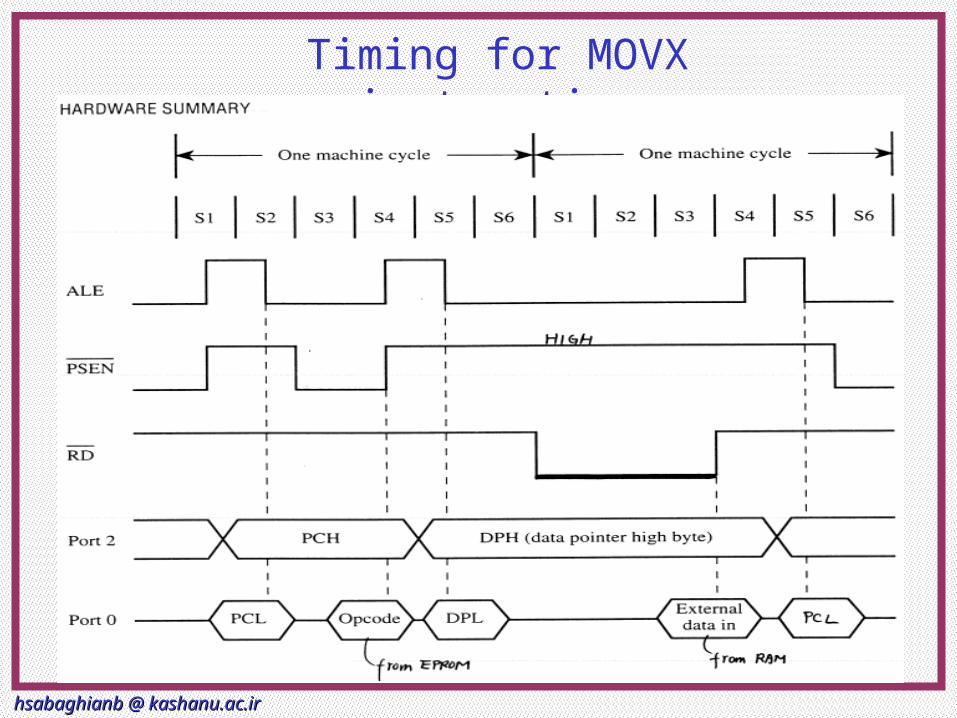
Timing for MOVX instruction
hsabaghianb @ kashanu.ac.irhsabaghianb @ kashanu.ac.ir MicroprocessorsMicroprocessors 4-4-4545
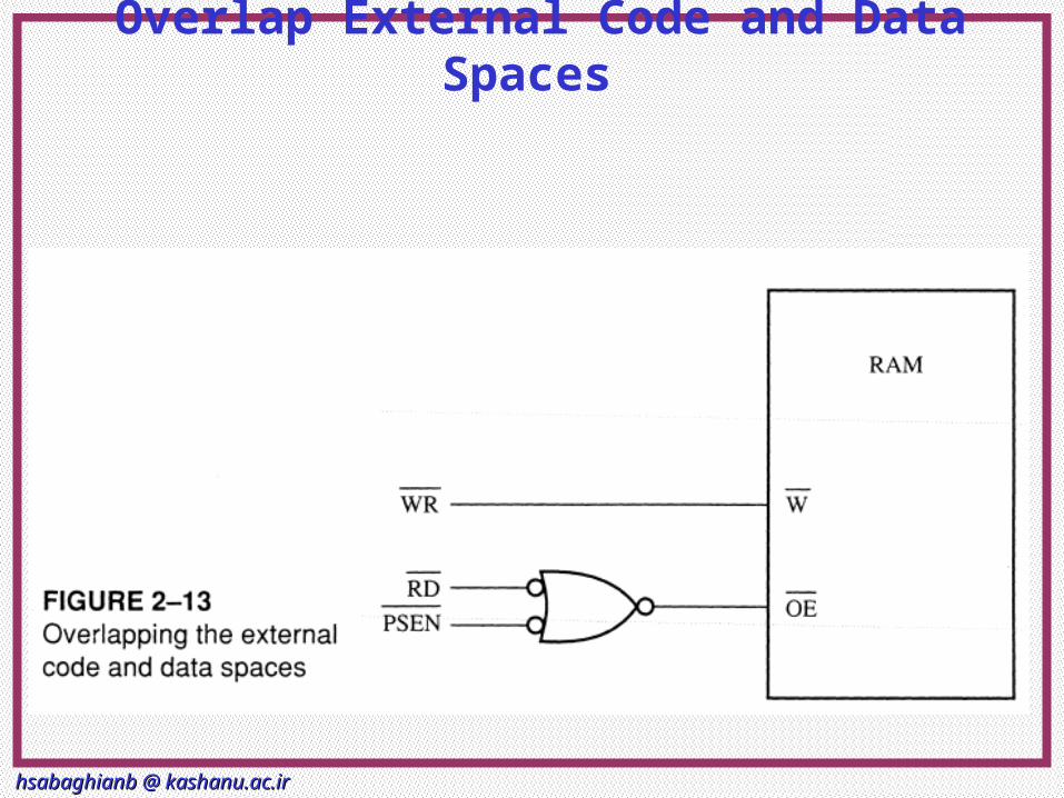
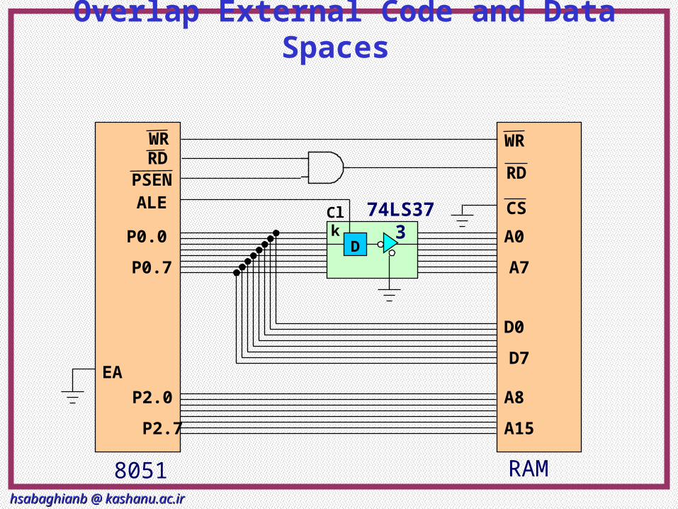
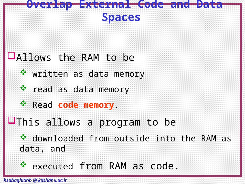
Overlap External Code and Data Spaces
hsabaghianb @ kashanu.ac.irhsabaghianb @ kashanu.ac.ir MicroprocessorsMicroprocessors 4-4-4646
RAM8051
D
74LS373ALE
P0.0
P0.7
PSEN
A0
A7
D0
D7
P2.0
P2.7
A8
A15
RD
CS
EA
Clk
RDWR WR
Overlap External Code and Data Spaces
hsabaghianb @ kashanu.ac.irhsabaghianb @ kashanu.ac.ir MicroprocessorsMicroprocessors 4-4-4747
Allows the RAM to be
written as data memory
read as data memory
Read code memory.
This allows a program to be
downloaded from outside into the RAM as data, and
executed from RAM as code.
Overlap External Code and Data Spaces
hsabaghianb @ kashanu.ac.irhsabaghianb @ kashanu.ac.ir MicroprocessorsMicroprocessors 4-4-4848
hsabaghianb @ kashanu.ac.irhsabaghianb @ kashanu.ac.ir MicroprocessorsMicroprocessors 4-4-4949
On-Chip Memory Internal RAM
hsabaghianb @ kashanu.ac.irhsabaghianb @ kashanu.ac.ir MicroprocessorsMicroprocessors 4-4-5050
General Purpose Register
0706050403020100
R7R6R5R4R3R2R1R0
0F
08
17
10
1F
18
Bank 3
Bank 2
Bank 1
Bank 0
4 Register BanksEach bank has R0-R7Selectable by PSW.2,3
hsabaghianb @ kashanu.ac.irhsabaghianb @ kashanu.ac.ir MicroprocessorsMicroprocessors 4-4-5151
Bit Addressable Memory
20h – 2Fh )16 locations 8-bits = 128 bits(
7F 78
1A
10
0F 08
07 06 05 04 03 02 01 00
27
26
25
24
23
22
21
20
2F
2E
2D
2C
2B
2A
29
28
Bit addressing:mov C, 1Ahormov C, 23h.2
hsabaghianb @ kashanu.ac.irhsabaghianb @ kashanu.ac.ir MicroprocessorsMicroprocessors 4-4-5252
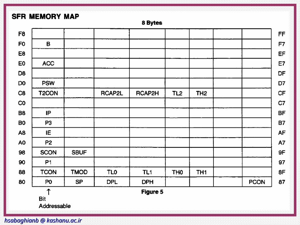
Special Function Registers
DATA registers
CONTROL registersTimersSerial portsInterrupt systemAnalog to Digital converterDigital to Analog converterEtc.
Addresses 80h – FFh
Direct Addressing used to access SFRs
hsabaghianb @ kashanu.ac.irhsabaghianb @ kashanu.ac.ir MicroprocessorsMicroprocessors 4-4-5353
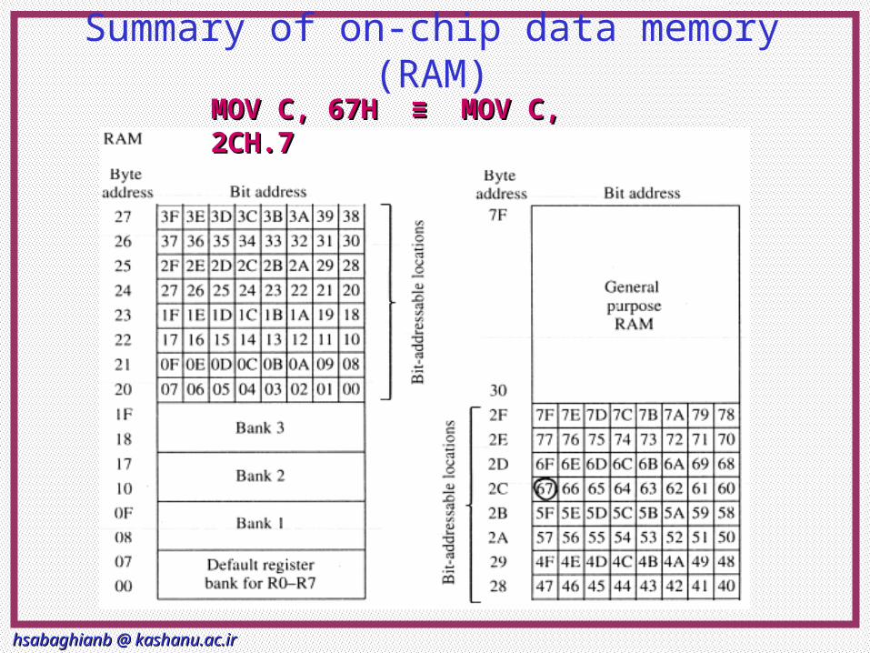
Summary of on-chip data memory (RAM)
MOV C, 67H ≡ MOV C, MOV C, 67H ≡ MOV C, 2CH.72CH.7
hsabaghianb @ kashanu.ac.irhsabaghianb @ kashanu.ac.ir MicroprocessorsMicroprocessors 4-4-5454
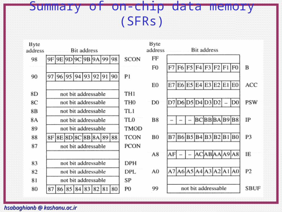
Summary of on-chip data memory (SFRs)
hsabaghianb @ kashanu.ac.irhsabaghianb @ kashanu.ac.ir MicroprocessorsMicroprocessors 4-4-5555
hsabaghianb @ kashanu.ac.irhsabaghianb @ kashanu.ac.ir MicroprocessorsMicroprocessors 4-4-5656
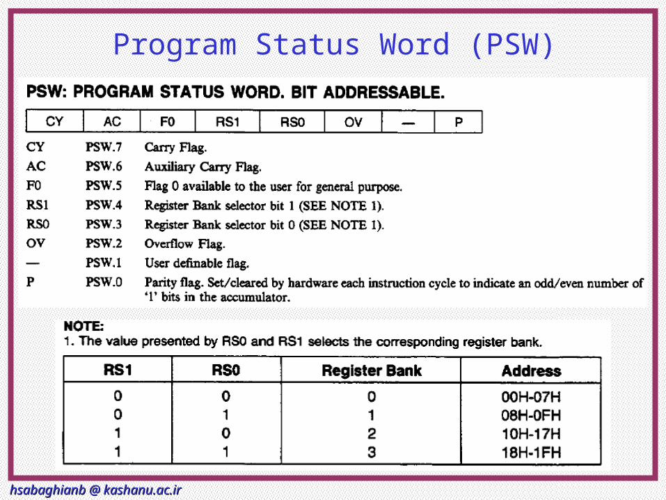
Program Status Word (PSW)
hsabaghianb @ kashanu.ac.irhsabaghianb @ kashanu.ac.ir MicroprocessorsMicroprocessors 4-4-5757
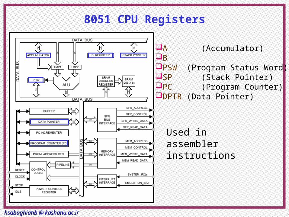
8051 CPU Registers
A (Accumulator)BPSW (Program Status Word)SP (Stack Pointer)PC (Program Counter)DPTR (Data Pointer)
Used in assembler instructions
hsabaghianb @ kashanu.ac.irhsabaghianb @ kashanu.ac.ir MicroprocessorsMicroprocessors 4-4-5858
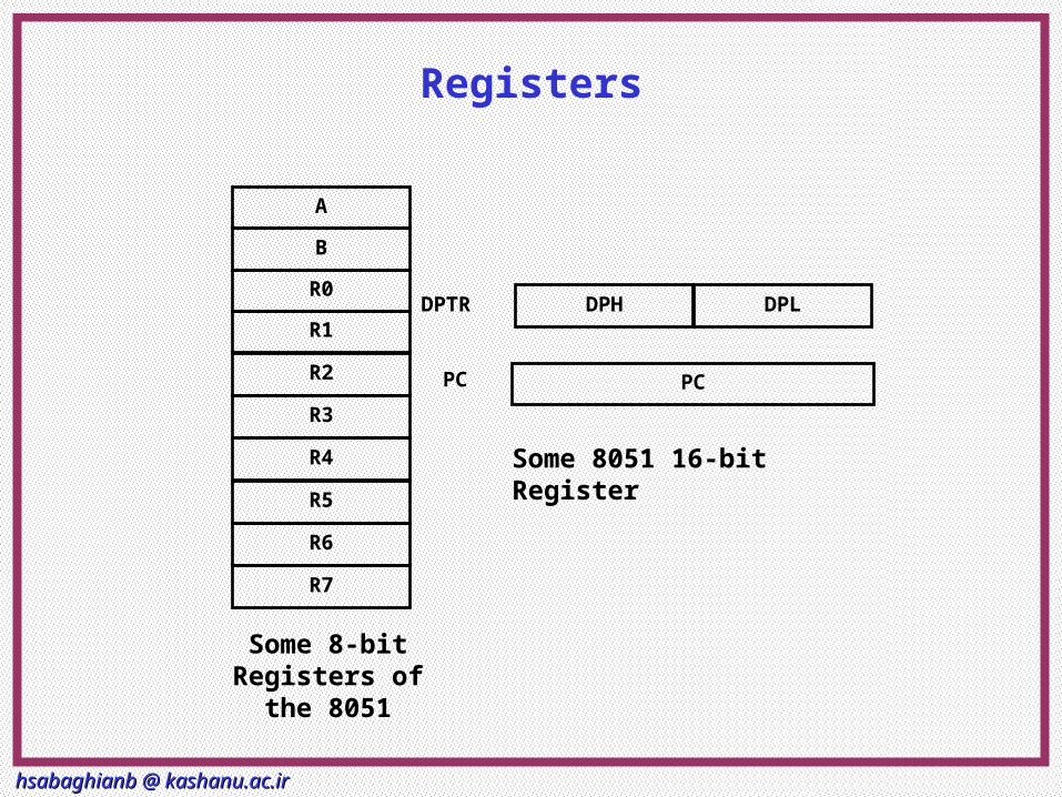
Registers
A
B
R0
R1
R3
R4
R2
R5
R7
R6
DPH DPL
PC
DPTR
PC
Some 8051 16-bit Register
Some 8-bit Registers of the 8051
hsabaghianb @ kashanu.ac.irhsabaghianb @ kashanu.ac.ir MicroprocessorsMicroprocessors 4-4-5959
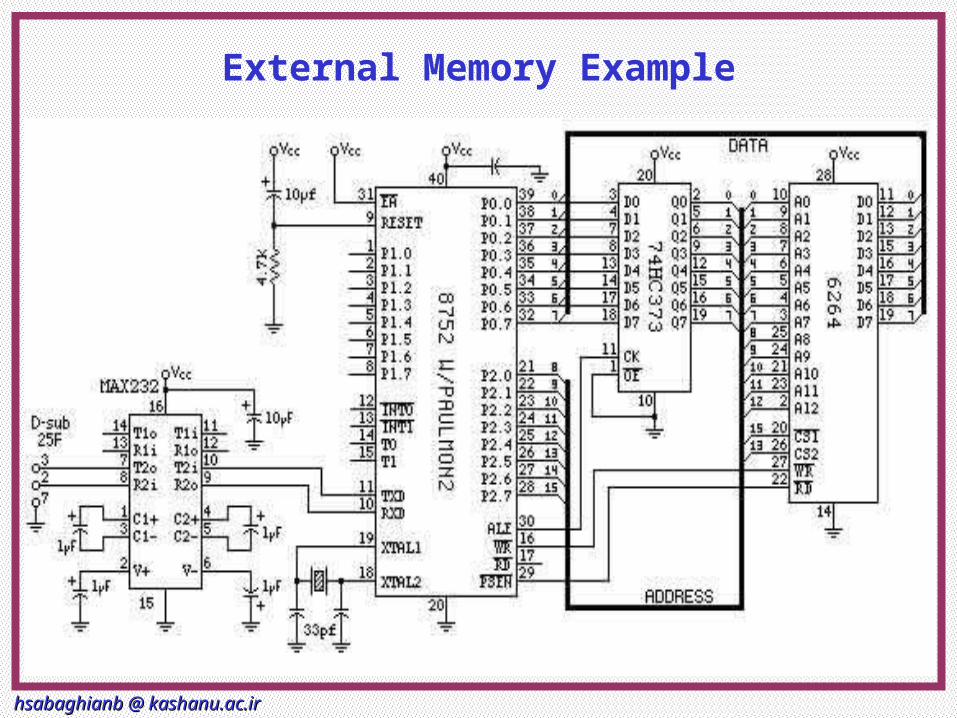
External Memory Example