Embed Size (px)
Citation preview
V I S H A Y S E M I C O N D U C T O R S
Rectifiers Application Note
How to Design an Rg Resistor for a Vishay Trench PT IGBT
www.vishay.com
AP
PL
ICA
TIO
N N
OT
E
Revision: 17-May-16 Document Number: 95690For technical questions within your region: [email protected], [email protected], [email protected]
THIS DOCUMENT IS SUBJECT TO CHANGE WITHOUT NOTICE. THE PRODUCTS DESCRIBED HEREIN AND THIS DOCUMENTARE SUBJECT TO SPECIFIC DISCLAIMERS, SET FORTH AT www.vishay.com/doc?91000
By Carmelo Sanfilippo and Filippo Crudelini
INTRODUCTIONIn low-switching-frequency applications like DC/AC stages for TIG welding equipment, the slow leg of a solar inverter, or a low-frequency converting structure where the maximum frequency is around 2 kHz, the IGBT has to guarantee the lowest possible conduction losses without switching losses affecting the device’s overall efficiency. Historically, these requirements have been fulfilled using the well-consolidated planar Punch Through (PT) IGBT technology.
In response to an increasing demand for efficiency in the applications mentioned above, Vishay recently released a new technology approach that combines the benefits of a PT design with the advantages of a new MOS Trench structure. The overall electrical performances of the resulting PT Trench IGBT structure are further enhanced with an optimized lifetime killing technology.
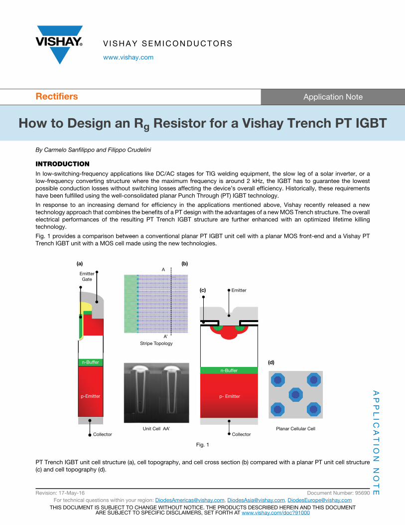
Fig. 1 provides a comparison between a conventional planar PT IGBT unit cell with a planar MOS front-end and a Vishay PT Trench IGBT unit with a MOS cell made using the new technologies.
Fig. 1
PT Trench IGBT unit cell structure (a), cell topography, and cell cross section (b) compared with a planar PT unit cell structure (c) and cell topography (d).
EmitterGate
A
A’
Emitter
Collector Collector
(a) (b)
(c)
(d)
Stripe Topology
Unit Cell AA’ Planar Cellular Cell
n-Buffer
n-Buffer
p- Emitterp-Emitter

How to Design an Rg Resistor for a Vishay Trench PT IGBT
Application Notewww.vishay.com Vishay Semiconductors
AP
PL
ICA
TIO
N N
OT
E
Revision: 17-May-16 2 Document Number: 95690For technical questions within your region: [email protected], [email protected], [email protected]
THIS DOCUMENT IS SUBJECT TO CHANGE WITHOUT NOTICE. THE PRODUCTS DESCRIBED HEREIN AND THIS DOCUMENTARE SUBJECT TO SPECIFIC DISCLAIMERS, SET FORTH AT www.vishay.com/doc?91000
Vishay’s PT Trench IGBT technology achieves a significant improvement in overall performance by implementing these features:
• Faster turn-off capability due to the high hole confinement achieved by adopting the Trench MOS structure for the device’s front-end. This design aspect allows for efficient hole accumulation close to the device’s base junction, where the carrier has a quicker response during device turn-off.
• Lower VCE(sat) due to high cell density, an optimized doping profile, and lifetime killing technology.
• Device robustness due to an optimized doping profile and lifetime killing process.
PT Trench IGBT technology is capable of guaranteeing a maximum junction temperature of +150 °C, showing a temperature coefficient for the main electrical parameters that is comparable with planar IGBT technology. The MOS Trench structure of the device’s front-end leads to different Cge, Crss capacitance, and dynamic behavior compared to planar devices, and these differences need to be taken into consideration when using a PT Trench IGBT.
CALCULATING THE GATE RESISTORThe gate driver circuit is made from a driver with an internal resistance, the connection between the driver circuit and the power module (twisted wire or PCB), and the internal layout of the IGBT module (internal connection, wire bonding, or chip in parallel).
The connection between the driver and IGBT terminal is a second-order circuit because it has an inductance and the gate of the IGBT does not have a negligible capacitance. A simplified electric model of the circuit is show in Fig. 2.
Fig. 2 Fig. 3
The gate driver usually has low series resistance and negligible inductance if the output stage is a transistor output. If the output is a pulse transformer, the inductance must be evaluated and taken into account.
The connection between the gate driver and IGBT can be a wire or PCB, as show in Fig. 4. The inductance of wire connections varies by the type of cable, the number of twists per inch, diameter, length, etc. For PCB connections, stray inductance varies by the track layout.
Fig. 4
In addition, at the external inductance there is internal inductance of the module due to the connection between the gate terminal and gate pad on the IGBT chip.
Driver
Wire Inductance Module InductanceEQ IGBT
Ciss1
Rg
RDriver
Driver
Stray InductanceIGBT
Ciss
RgRDriver 1
DIAP
SOT-227 SOT-227b

How to Design an Rg Resistor for a Vishay Trench PT IGBT
Application Notewww.vishay.com Vishay Semiconductors
AP
PL
ICA
TIO
N N
OT
E
Revision: 17-May-16 3 Document Number: 95690For technical questions within your region: [email protected], [email protected], [email protected]
THIS DOCUMENT IS SUBJECT TO CHANGE WITHOUT NOTICE. THE PRODUCTS DESCRIBED HEREIN AND THIS DOCUMENTARE SUBJECT TO SPECIFIC DISCLAIMERS, SET FORTH AT www.vishay.com/doc?91000
The following table indicates the internal inductance of the modules where PT IGBT chips are mounted.
This internal inductance is the equivalent of the inductance in-series at the gate-emitter connection, and is a function of the dimensions of the module.
The GP250 is a SOT-227 device with a very short gate-emitter connection and has a low inductance compared to the GP400, which is a larger DIAP module with several chips in parallel and a large gate connection.
To perform a practical evaluation of a gate circuit, consider a gate mesh circuit equivalent to that in Fig. 3, where it is possible to add up the values of the elements in series.
The VGE voltage that switches the IGBT on and off is the voltage across a capacitor, Ciss, of the LC series circuit. This can be a problem because if the Q of the circuit is larger than 1, there will be oscillation on the VGE that is not acceptable in certain cases. The Q of the circuit is a function of Lstray, Ciss, and Rg.
Lstray is related to the layout of the circuit, the driver, and the connection between the driver and IGBT.
The driver and gate connection has a very different inductance value, as a function of the layout, but it is a fixed value within the working conditions of the circuit.
The Ciss is the capacitance seen from the gate pin, which is the sum of internal capacitance Cge and Cgc. This capacitance changes with the VGE, VCE, and temperature. Fig. 5 shows the behavior of the Ciss, Crss, and Coss as functions of the VCE.
Fig. 5 - Ciss = Cge + Cgc, Crss = Cgc, Coss = Cce + CgcFig. 6
Fig. 5 shows the capacitance of the GP100TS60, a large single-die device in the IAP. The capacitance varies with voltage and temperature, so evaluating the correct Rg value for the circuit in all conditions requires a field test.
A preliminary evaluation of Rg is possible, using the following formula, if there is an estimation of stray inductance:
TABLE 1LS MODULE
GP250 12
GP100 30
GP300 87
GP400 114
Cap
acit
ance
(n
F)
VCE (V)
1 10 100 10001
1000
10
100
Ciss
Coss
Crss
GP100TS60
Collector
Emitter
Gate
Cce
Cgc
Cge
Rg 1.2Lstraymodule Lgate cable+
Ciss at VCE 0 V= ------------------------------------------------------------------- 1 =

How to Design an Rg Resistor for a Vishay Trench PT IGBT
Application Notewww.vishay.com Vishay Semiconductors
AP
PL
ICA
TIO
N N
OT
E
Revision: 17-May-16 4 Document Number: 95690For technical questions within your region: [email protected], [email protected], [email protected]
THIS DOCUMENT IS SUBJECT TO CHANGE WITHOUT NOTICE. THE PRODUCTS DESCRIBED HEREIN AND THIS DOCUMENTARE SUBJECT TO SPECIFIC DISCLAIMERS, SET FORTH AT www.vishay.com/doc?91000
This value of Rg can be used as a first value for testing in the circuit. The final value can be fixed as a function of the different requirements in the circuit.
As an example we consider a circuit made with the GP100TS60. The module is connected to the driver with a twisted pair cable that is 25 cm long.
Fig. 7
The twisted pair cable (3 turn / cm) has a total inductance of 230 nH. The internal inductance of the module is 30 nH. The IGBT Ciss is 33 nF at VCE = 0 V.
Using the formula (1) discussed above, we can determine that the Rg value is ≈ 3.3 . This number is the initial value that can be used in a circuit for the preliminary test.
In a practical case the real inductance of the cable is only estimated or is unknown. The Ciss changes in respect to the operating conditions, so a field test is necessary to optimize the Rg, especially because Rg not only dumps the mesh gate but can control dl/dt and dV/dt - changing overshot and noise.
In the real circuit there are three common situations. The first is a large Rg with the gate signal behavior shown in Fig. 8. Here, the device is the GP100TS60 with Rg = 10 and a 25 cm twisted pair cable. The C4 green track is the IG, and the C1 blue track is the VGE measured on the gate terminal as close as possible to the module. C2 cyan track VCE is equal to 0 because only the effect of Cge is considered.
This condition guarantees a smooth transition and that the voltage VGE does not exceed the plateau limit. During turn-on the current flows only in a positive direction, and during turn-off it only flows in a negative direction.
The advantage of this kind of driving circuit is that the noise is very low, and a low current is required from the driver. The disadvantage is that Eon and Eoff are not the minimum.
Fig. 8
How to Design an Rg Resistor for a Vishay Trench PT IGBT
Application Notewww.vishay.com Vishay Semiconductors
AP
PL
ICA
TIO
N N
OT
E
Revision: 17-May-16 5 Document Number: 95690For technical questions within your region: [email protected], [email protected], [email protected]
THIS DOCUMENT IS SUBJECT TO CHANGE WITHOUT NOTICE. THE PRODUCTS DESCRIBED HEREIN AND THIS DOCUMENTARE SUBJECT TO SPECIFIC DISCLAIMERS, SET FORTH AT www.vishay.com/doc?91000
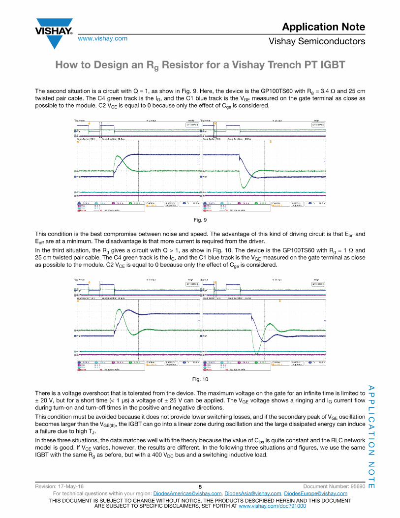
The second situation is a circuit with Q ≈ 1, as show in Fig. 9. Here, the device is the GP100TS60 with Rg = 3.4 and 25 cm twisted pair cable. The C4 green track is the IG, and the C1 blue track is the VGE measured on the gate terminal as close as possible to the module. C2 VCE is equal to 0 because only the effect of Cge is considered.
Fig. 9
This condition is the best compromise between noise and speed. The advantage of this kind of driving circuit is that Eon and Eoff are at a minimum. The disadvantage is that more current is required from the driver.
In the third situation, the Rg gives a circuit with Q > 1, as show in Fig. 10. The device is the GP100TS60 with Rg = 1 and 25 cm twisted pair cable. The C4 green track is the IG, and the C1 blue track is the VGE measured on the gate terminal as close as possible to the module. C2 VCE is equal to 0 because only the effect of Cge is considered.
Fig. 10
There is a voltage overshoot that is tolerated from the device. The maximum voltage on the gate for an infinite time is limited to ± 20 V, but for a short time (< 1 μs) a voltage of ± 25 V can be applied. The VGE voltage shows a ringing and IG current flow during turn-on and turn-off times in the positive and negative directions.
This condition must be avoided because it does not provide lower switching losses, and if the secondary peak of VGE oscillation becomes larger than the VGE(th), the IGBT can go into a linear zone during oscillation and the large dissipated energy can induce a failure due to high TJ.
In these three situations, the data matches well with the theory because the value of Ciss is quite constant and the RLC network model is good. If VCE varies, however, the results are different. In the following three situations and figures, we use the same IGBT with the same Rg as before, but with a 400 VDC bus and a switching inductive load.

How to Design an Rg Resistor for a Vishay Trench PT IGBT
Application Notewww.vishay.com Vishay Semiconductors
AP
PL
ICA
TIO
N N
OT
E
Revision: 17-May-16 6 Document Number: 95690For technical questions within your region: [email protected], [email protected], [email protected]
THIS DOCUMENT IS SUBJECT TO CHANGE WITHOUT NOTICE. THE PRODUCTS DESCRIBED HEREIN AND THIS DOCUMENTARE SUBJECT TO SPECIFIC DISCLAIMERS, SET FORTH AT www.vishay.com/doc?91000
The first situation is a large Rg with gate signal behavior, as shown in Fig. 11. The device is the GP100TS60 with Rg = 10 and 25 cm twisted pair cable. The C4 green track is the IG, C1 blue track is the VGE, C2 light blue is the VCE, and C3 purple is the IC.
Fig. 11
This condition guarantees a smooth transition and that the VGE does not exceed the positive and negative plateau limit. The IRRM induced in the freewheeling diode is very low. The switching current is 120 A and the peak at the turn-on is 150 A, meaning that the IRRM of the diode is only 30 A.
Now, with a large VCE, there are evident effects due to the Crss on the gate voltage. The Miller plateau in a high-voltage device is different from the effects that are usually expected in low-voltage devices like power MOSFETs.
Fig. 12
Fig. 12 shows a comparison between a high-voltage Trench device and the behavior of a low-voltage MOSFET.
The behavior of VCE is magnified to clarify the effect.
Soft VCE voltage is normal during transition and it is almost invisible. It is less than 10 V to 15 V with time ≈ 400 ns and it is a normal behavior that is not usually due to poor driving. If VCE show higher level and longer time the VGE is usually poor and it has oscillation that is the signature of improper gate driving.
By applying the Miller theorem, a simple approximation of Ciss can be written as:
Ciss (VGE, VCE) = Cge (VGE) + Crss (VCE)(1 + AV (ICE, VCE, VGE)
In a low-voltage device there is a large AV during the voltage transition. This is also true in a high-voltage device, but Crss is small, so the maximum of the product Crss (VCE) 1 + (AV (ICE, VCE, VGE)) is when VCE is around 20 V to 30 V.
VGE
VGE(th)
VCE IC
VDS fall forlow voltage MOSFETs
VCE fall forPT IGBT
Timet0 t4t3t2t1

How to Design an Rg Resistor for a Vishay Trench PT IGBT
Application Notewww.vishay.com Vishay Semiconductors
AP
PL
ICA
TIO
N N
OT
E
Revision: 17-May-16 7 Document Number: 95690For technical questions within your region: [email protected], [email protected], [email protected]
THIS DOCUMENT IS SUBJECT TO CHANGE WITHOUT NOTICE. THE PRODUCTS DESCRIBED HEREIN AND THIS DOCUMENTARE SUBJECT TO SPECIFIC DISCLAIMERS, SET FORTH AT www.vishay.com/doc?91000
This effect changes the switching evolution. The real required Qg is higher than the Qg estimated from the capacitance. For this reason it is better use the Qg data in the datasheet to evaluate the required power for the driver.During the turn-off transition, it is possible to see two different slopes in the current IC. In the first portion of current transition, the IC drops quickly with a voltage overshoot. The peak arrives at 530 V; this is the MOSFET transition. The second portion is an exponential decay typical of bipolar recombination and does not produce any overshoot.In the second situation, the Rg gives an input circuit with Q ≈ 1 as shown in Fig. 13. The device is the GP100TS60 with Rg = 3.4 and a 25 cm twisted pair cable. The C4 green track is the IG, C1 blue track is the VGE, C2 light blue is the VCE, and C3 purple is the IC.
Fig. 13
Here, the IG current does not show oscillation. During turn-on the current flow is only in a positive direction, and only in a negative direction during turn-off. This means that the VGE is strictly increasing or strictly decreasing.The IGBT stays in a linear zone only for the minimum time, the losses due to multiple transitions are avoided, and VCE is as low as possible.The IRRM induced in the freewheeling diode in this configuration is higher. The switching current is 120 A and the peak at turn-on is 182 A. This means that the IRRM of the diode is 62 A, but that the Eon losses are smaller because time is shorter. The peak of the IG current is higher but the Qg is similar, because the required charge for turn-on and turn-off is not strongly dependent on Rg.Usually, the peak current in the driver is evaluated as
Using this formula in this configuration with VCC = 18 V, VEE = 0 V, VDR = 1 V (VCC is the positive supply voltage of the driver, VEE is the negative supply voltage of the driver, and VDR is the voltage drop for the driver), and Rg = 3.4 , the formula (2) gives a maximum IG of 5 A. As is possible to see from Fig. 13, the IG peak is -2.3 A. This is because the formula (2) considers only the resistive part of the gate mesh that is a very worst case scenario, like removing the module, or the wire from the driver, and closing the driver on a short circuit. This consideration leads to choosing an oversized driver that is not required for this kind of application.Usually when the Q of an RLC network is ≈ 1, it is possible to choose a driver that has:
At the normal max. switching frequency of 1 kHz to 2 kHz, the required power is very low due to 2 x Qg x fsw being very low.Also in this case, the behavior at turn-off shows a double slope. The first portion of current transition of the IC drops quickly, inducing an overshoot peak that arrives at 570 V. The MOSFET transition and electric field recovery are heavily influenced by the Rg; with Rg = 10 to Rg = 3.4 , the overvoltage peak pass is from 530 V to 570 V. The second portion is an exponential decay of bipolar recombination that is quite independent from the Rg, so it does not change the behavior much.The disadvantage here is that the voltage overshoot is higher, but that is not an issue for this device. Instead, it is the high dl/dt and dV/dt that can be a problem in terms of EMI. In regards to turn-off losses, the difference in Eoff between devices that are
IG max.
VCC VEE VDR– –
Rg------------------------------------------------ 2 =
IG max.
VCC VEE VDR– –
2 x Rg------------------------------------------------=

How to Design an Rg Resistor for a Vishay Trench PT IGBT
Application Notewww.vishay.com Vishay Semiconductors
AP
PL
ICA
TIO
N N
OT
E
Revision: 17-May-16 8 Document Number: 95690For technical questions within your region: [email protected], [email protected], [email protected]
THIS DOCUMENT IS SUBJECT TO CHANGE WITHOUT NOTICE. THE PRODUCTS DESCRIBED HEREIN AND THIS DOCUMENTARE SUBJECT TO SPECIFIC DISCLAIMERS, SET FORTH AT www.vishay.com/doc?91000
driven with Rg = 10 and Rg = 3.4 is negligible; the reduction of Rg does not give a particular advantage in terms of switching losses. This explains how it is possible use a different Rg to change the dl/dt and dV/dt to solve the EMI problem without modifying the layout of the circuit.If we consider turn-on, reducing the Rg decreases the Eon losses. For example, the GP100TS60 with an Eon of Rg = 10 gives 7.3 mJ of losses for each commutation. Compared to an Eon of Rg = 3.4 with 4.8 mJ of losses, the gain is huge.If we think that a reasonable maximum switching frequency can be 2 kHz, the gain in terms of power is 5 W. For a device that handles 120 A, this is a small portion of the total losses.In regards to turn-off, the Eoff difference between a device that is driven with Rg = 10 and Rg = 3.4 is negligible; the same reduction in Rg does not give a particular advantage in terms of switching losses.This explains how it is possible to use a different Rg to change the dl/dt and dV/dt to solve the EMI problem without modifying the layout.In the third situation, the Rg provides a circuit with Q > 1, as show in Fig. 14. The device is the GP100TS60 with Rg = 1 and a 25 cm twisted pair cable. The C4 green track is the IG, C1 blue track is the VGE measured on the gate terminal as close as possible to the module, C2 light blue is the VCE, and C3 purple is the IC.
Fig. 14
The IG current shows an oscillation during turn-on and turn-off, with the current flowing in a positive and negative direction. This behavior is reflected in an oscillation of the VGE, which can be tolerated if the level of VGE guarantees the state of the IGBT. Guaranteeing the state of the IGBT means that the VGE voltage is high enough to assure a low VCE when the IGBT is on, and low enough to assure a negligible IC when the IGBT is off.In Fig. 15, which it is an enlargement of the left side of Fig. 14, two kinds of oscillation are present. The first is due to ringing on the gate from too low Rg (compared with the VGE voltage in Fig. 10), and the second is noise due to the ringing on VCE produced by the quick recovery of the diode induced from the very high dl/dt.
Fig. 15
Envelope of VGE
Incompletely closed IGBT due to low VGE
VGE level that guarantees IGBT closed with 120 A

How to Design an Rg Resistor for a Vishay Trench PT IGBT
Application Notewww.vishay.com Vishay Semiconductors
AP
PL
ICA
TIO
N N
OT
E
Revision: 17-May-16 9 Document Number: 95690For technical questions within your region: [email protected], [email protected], [email protected]
THIS DOCUMENT IS SUBJECT TO CHANGE WITHOUT NOTICE. THE PRODUCTS DESCRIBED HEREIN AND THIS DOCUMENTARE SUBJECT TO SPECIFIC DISCLAIMERS, SET FORTH AT www.vishay.com/doc?91000
The high-frequency noise has a short period of < 25 ns, which is shorter than the td of the IGBT. For this reason, the modulation of conduction is negligible and the quick variation of VCE is due to high-frequency current on the stray inductance of the module.
The average value of VCE, which shows a sort of tail, demonstrates the low value of VGE to carry 120 A. However, as is underlined in the instantaneous power (M-channel red track), the energy dissipated during this time is a small portion of the total energy.
There is a slow variation of VGE after the turn-on change, but the value of VGE does not go under the level that guarantees low VCE. At the time indicated from the vertical slotted line, the local minimum is higher than 15 V.
If the oscillation of VGE becomes greater, the IGBT could have a poor VCE, which increases the losses that add to the Eoff. For this reason, a suggested VGE is around 18 V instead of the typical 15 V. 15 V is a good value, but must be guaranteed in any condition. If there is any doubt about the ability to guarantee 15 V in any condition, it is better to use a VGE of 18 V or more. PT IGBT technology can work fine with VGE near 20 V, and for a short time values of ± 25 V are safe.
Analyzing the turn-off in Fig. 14, we can see that oscillations on the current are longer and the Q of the circuit at turn-off is higher than at turn-on. This effect is due to the non-linear behavior of Ciss with the VCE. For comparison, in Fig. 10 turn-on and turn-off are very similar because the VCE is zero. Also in this case, it is possible to see two different kinds of oscillation. The lowest-frequency oscillation is related to the RLC circuit in the gate mesh. The quick oscillation in reality is noise due to the projection of VCE on VGE through the Crss.
Fig. 16
In Fig. 16 there is an enlargement of Fig. 14. The slow oscillation carries the VGE at a voltage lower than zero, which is not an issue but helps to switch off the MOSFET quickly, resulting in an overshoot of 580 V.
After the negative VGE rise at a positive value, which can put the IGBT in conduction, a cross conduction of the IGBT leg with large dissipated energy can be produced.
To avoid this effect, it is usually better to drive the IGBT with a VGE of negative value, but the PT Trench device does not require this feature on the driver in a normal condition. The real threshold voltage is high enough to guarantee a good margin and avoid cross conduction. This simplifies the design of the driver and avoids a negative voltage supply.
-1000100200300400500600700
-30
-20
-10
0
10
20
30
-0.50 -0.45 -0.40 Col
lect
or p
aram
ter
VC
E V
IC A
Gat
e p
aram
eter
VG
E V
IG
A
Time (μs)
VGE CH1
IG CH4
VCE CH2
IC CH3
GP100TS60 Turn Off

How to Design an Rg Resistor for a Vishay Trench PT IGBT
Application Notewww.vishay.com Vishay Semiconductors
AP
PL
ICA
TIO
N N
OT
E
Revision: 17-May-16 10 Document Number: 95690For technical questions within your region: [email protected], [email protected], [email protected]
THIS DOCUMENT IS SUBJECT TO CHANGE WITHOUT NOTICE. THE PRODUCTS DESCRIBED HEREIN AND THIS DOCUMENTARE SUBJECT TO SPECIFIC DISCLAIMERS, SET FORTH AT www.vishay.com/doc?91000
Fig. 17
An IC around 1 A is not an issue for a short time (500 ns to 1000 ns) because the related energy is not too large. From this number with the data in Fig. 17, which shows the VGE(th) voltage, it is possible to evaluate the critical value of VGE. For an IC of 1 A at high temperature, the VGE is around 5 V. If the VGE ringing is lower than this value, the PT IGBT does not show a false turn-on or cross conduction problem. In Fig. 16, the maximum VGE after commutation is around 3 V, which is a safe value.
At lower temperatures the margin is higher and the necessity for a negative VGE is completely avoided. Note that in Fig. 17, the problem is not guaranteeing the off state at a low temperature, but having VGE high enough to guarantee a low VCE when the IGBT is in the on state after turn-on. For this reason as well, a VGE larger than 15 V is often preferred.
In Fig. 16 there is a spike on VGE voltage due to the quick variation on VCE. During turn-off the gate mesh must be extended at Crss because the current from the Crss capacitor could be comparable with the current from the driver.
Fig. 18
Fig. 18 shows a simplified circuit of an IGBT during turn-off. When VCE increases, the Cgc capacitor requires a current that flows
in the gate node, increasing the VGE because the current drained from the driver is and the current that
arrives from the Cgc is . VGE is usually negligible compared with VCE, so VCG ≈ VCE.
At a high VCE, the Crss is small but is very high. The current IRg1 during this transient is quite constant, because it is forced
from the inductance LS. So the value of VGE is defined by the ratio between Cgc and Cge.
-0.2
0
0.2
0.4
0.6
0.8
1.0
1.2
1.4
0 2 4 6 8 10
I C (A
)
VGE (V)
TJ = 125 °CTJ = 25 °CTJ = -40 °C
VGE(th)
Driver
LSRg1RDriver 2
Cge
Cgc
IGBT1
E
C
IRG1
VGE - VDR
2 Rg1 + RDriver ------------------------------------------
ICgc Cgc VCE dVCE
dt--------------
dVCE
dt--------------

How to Design an Rg Resistor for a Vishay Trench PT IGBT
Application Notewww.vishay.com Vishay Semiconductors
AP
PL
ICA
TIO
N N
OT
E
Revision: 17-May-16 11 Document Number: 95690For technical questions within your region: [email protected], [email protected], [email protected]
THIS DOCUMENT IS SUBJECT TO CHANGE WITHOUT NOTICE. THE PRODUCTS DESCRIBED HEREIN AND THIS DOCUMENTARE SUBJECT TO SPECIFIC DISCLAIMERS, SET FORTH AT www.vishay.com/doc?91000
Reducing the Rg can help to keep control of the VGE, but reducing Rg could produce oscillation due to the high Q factor of the RLC circuit. One simple solution if the connection between the driver and IGBT is long and has large inductance is to place a small capacitor in parallel at the gate.
Fig. 19
Fig. 19 shows the gate circuit with the auxiliary capacitor Cgaux, which must be mounted near the module or any inductance between the gate connection and the capacitor reduces its effect. The initial value of Cgaux can be equal to the value of Ciss at VCE without overshoot (substantially the DC bus value) or 15 % of Ciss at VCE = 0 V. The Rg must be revised with the same procedure at the formula (1), with the difference being that Ciss is now:
Driver
LS1Rg2RDriver 3
Cge1
Cgc1
IGBT2
E
C
Cgaux
Ciss + Cgaux x Rg = 1.2Lstraymodule + Lgate cable
Ciss at VCE = 0 V + Cgaux---------------------------------------------------------------------- 3

How to Design an Rg Resistor for a Vishay Trench PT IGBT
Application Notewww.vishay.com Vishay Semiconductors
AP
PL
ICA
TIO
N N
OT
E
Revision: 17-May-16 12 Document Number: 95690For technical questions within your region: [email protected], [email protected], [email protected]
THIS DOCUMENT IS SUBJECT TO CHANGE WITHOUT NOTICE. THE PRODUCTS DESCRIBED HEREIN AND THIS DOCUMENTARE SUBJECT TO SPECIFIC DISCLAIMERS, SET FORTH AT www.vishay.com/doc?91000
CONCLUSIONThe optimum Rg value for an application must take into account the working conditions and the trade off between efficiency and noise. In any case, the third condition presented in this application note must be avoided, and a signal with behavior similar to the VGE in Fig. 9 will give the best compromise between noise and switching losses. The third condition could reduce switching losses, but in a situation where switching losses are the small portion of global losses, the advantages in term of efficiency are negligible.
If there is noise induced from too high dV/dt or dl/dt, it is possible to control it with Rg.
The behavior of the IGBT during switching can be changed by choosing the right value of Rg and dV/dt across the CE terminal. If the Rg required is too large and the dVCE/dt injects noise at the gate, a small capacitor can be placed in parallel near the gate terminal. Usually VCE(t) changes with the Rg of an IGBT, but if the IGBT works in a circuit with soft switching, it is possible to control dl/dt and dV/dt independently from the Rg.
In general, there is feedback from the collector to the emitter between the Cgc that changes the real VGE across the gate of the IGBT. In this case, there are not general rules. Any circuit requires the appropriate value of Rg based on the required characteristic.
The behavior of the IGBT during turn-on and turn-off can be controlled through the Rg. The VCE overshoot can be controlled with Rg off, while the peak of IRRM in the diode can be controlled with Rg on. Many other parameters are influenced by Rg, as shown in Table 2.
The target of a good design is to obtain the highest efficiency but also have the right margin in terms of VCE and to respect EMI limits.
TABLE 2RATING / CHARACTERISTICS Rg Rg
td(on)
td(off)
Eon
Eoff
Erec
Turn on Ipk
Diode IRRM
dV/dt
dI/dt
Voltage overshot
EMI noise