Embed Size (px)
Citation preview

How do LEDs work?A little physics; a little basic semiconductor theory
18SPRING 2009
SPR
ING
200
8
18SPRING 2009
SPR
ING
200
9
CHATTING WITH SOME COLLEAGUES at the USITT show
in Cincinnati last week it occurred to me that, although we’ve
dug into many LED topics in this column, one thing we’ve never
talked about is how the darn things actually work. Most of the
light sources we use in entertainment luminaires produce light
using techniques we are familiar with from experience and natural
phenomena. We understand that if you heat an object to a high
enough temperature then it starts to glow red and emit light, so
the light output from a filament in an incandescent lamp isn’t
at all surprising. Similarly we’ve all seen lightning streak across
the sky and can make the mental connection between that and a
discharge lamp. Fluorescent lamps are a little harder to explain, but
again they rely upon effects seen in nature—a plasma discharge
and fluorescence converting the ultra-violet emissions from that
discharge into visible wavelengths. Similar fluorescence is seen
in many natural organisms both in plants and in animals, being
particularly common in ocean dwelling life forms. You don’t have
to go scuba diving to see examples of natural fluorescence though,
many butterflies have fluorescent pigments and I’m sure everyone
has noticed their finger nails glowing under UV or black light on
stage or at Halloween. Although not quite as bright as finger nails,
other keratin based substances such as wool and hair exhibit the
effect as well.
All of those are readily understandable but what on earth is
going on inside an LED to make it emit light? It isn’t any of the
phenomena we’ve just mentioned and doesn’t involve heat (except
as a by-product), an electric arc or fluorescence. Instead it’s a very
low level sub-atomic effect produced by the movement of electrons
within energy bands inside the device. I’m not going to dig too
deeply into the physics of this (even if I knew it) but it’s worth
taking a closer look at what’s going on.
LEDs are more properly known as Light Emitting Diodes and, as
the name suggests, normally consist of a single p-n junction diode.
But, hang on a minute, what’s a diode and what’s it got to do with
emitting light? A diode is the basic building block of solid state
electronics and is the simplest possible semiconductor device. The
fundamental electrical property of a semiconductor diode is that it
only allows electric current to flow in one direction, but how does it
do that? Most semiconductors are made of a poor conductor such
as silicon and germanium that has had atoms of another material
deliberately added to it. This process of adding these impurities is
often called doping. The original pure material is electrically neutral
and has exactly the right number of electrons associated with each
atom, meaning there are neither too many nor too few electrons
and so there are no free electrons available to carry electric current.
However the doping process of adding extra atoms moves some of
the electrons in the material and can leave a material with either
more free electrons than it needs in some parts or with too few,
thus leaving positively charged holes where electrons can fit. Both
these changes make the material more able to conduct an electric
current. In normal terminology the material with extra electrons
is called N-type, since those extra electrons are negatively charged
particles, and the material with a deficit of electrons (or surfeit
of holes) is called P-type. Because of the electrostatic attraction
between positive and negative particles free electrons are attracted
towards the positively charged holes.
A diode is a very simple device which uses one piece of N-type
material (with an excess of electrons) connected to another piece
of P-type material (with an excess of holes). The area where the
two materials meet is known as the junction. Figure 1 shows a
P N+
+
+ ++
++ -
--
--
-
-
Holes Electrons
Figure 1 – Initial diode formation
Out of the WoodBY MIKE WOOD
19PROTOCOL
SPRIN
G 2009
19PROTOCOL
SPRIN
G 2009
Out of the Wood | How do LEDs work?
. . . what on earth is going on inside an LED to make it emit light?“
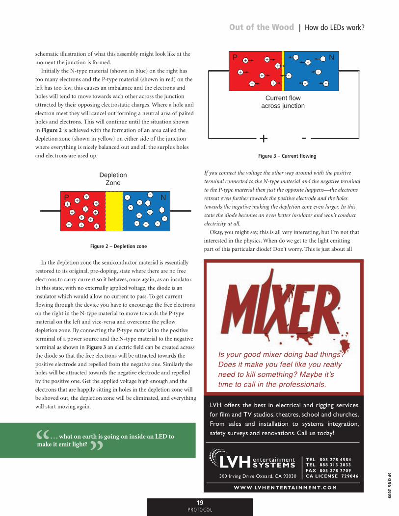
“schematic illustration of what this assembly might look like at the
moment the junction is formed.
Initially the N-type material (shown in blue) on the right has
too many electrons and the P-type material (shown in red) on the
left has too few, this causes an imbalance and the electrons and
holes will tend to move towards each other across the junction
attracted by their opposing electrostatic charges. Where a hole and
electron meet they will cancel out forming a neutral area of paired
holes and electrons. This will continue until the situation shown
in Figure 2 is achieved with the formation of an area called the
depletion zone (shown in yellow) on either side of the junction
where everything is nicely balanced out and all the surplus holes
and electrons are used up.
Figure 2 – Depletion zone
In the depletion zone the semiconductor material is essentially
restored to its original, pre-doping, state where there are no free
electrons to carry current so it behaves, once again, as an insulator.
In this state, with no externally applied voltage, the diode is an
insulator which would allow no current to pass. To get current
flowing through the device you have to encourage the free electrons
on the right in the N-type material to move towards the P-type
material on the left and vice-versa and overcome the yellow
depletion zone. By connecting the P-type material to the positive
terminal of a power source and the N-type material to the negative
terminal as shown in Figure 3 an electric field can be created across
the diode so that the free electrons will be attracted towards the
positive electrode and repelled from the negative one. Similarly the
holes will be attracted towards the negative electrode and repelled
by the positive one. Get the applied voltage high enough and the
electrons that are happily sitting in holes in the depletion zone will
be shoved out, the depletion zone will be eliminated, and everything
will start moving again.
Figure 3 – Current flowing
If you connect the voltage the other way around with the positive
terminal connected to the N-type material and the negative terminal
to the P-type material then just the opposite happens—the electrons
retreat even further towards the positive electrode and the holes
towards the negative making the depletion zone even larger. In this
state the diode becomes an even better insulator and won’t conduct
electricity at all.
Okay, you might say, this is all very interesting, but I’m not that
interested in the physics. When do we get to the light emitting
part of this particular diode? Don’t worry. This is just about all
P N++
+ ++ +
++
+
+
+ +
--
-
- -
--
-
-
---
Depletion
Zone
P N+
+
+ ++
++ -
--
--
-
-
Current flow
across junction
+ -
Is your good mixer doing bad things? Does it make you feel like you really need to kill something? Maybe it’s time to call in the professionals.
LVH offers the best in electrical and rigging services
for film and TV studios, theatres, school and churches.
From sales and installation to systems integration,
safety surveys and renovations. Call us today!

20SPRING 2009
SPR
ING
200
9
the theory we need to understand the principles of the process
but there’s no avoiding a little delving in the bowels of basic
semiconductor theory.
In a light emitting diode everything behaves exactly the same
as in the diode illustrated here and, in fact, most diodes are light
emitting to some extent, but the light might be invisible. LEDs are
operated in the connection shown in Figure 3 (known as forward
biased) where the diode is connected such that current flows
through the device and electrons and holes are continually moving
and meeting at the junction and being replenished from the
applied electric voltage. It’s what happens when those electrons and
holes meet up that actually generates the light.
Figure 4 – Electron and hole combine
As shown diagrammatically in Figure 4 a free electron in the
conduction band of the semiconductor has an energy level higher
than the energy level of the hole. When the high energy electron
drops into a low energy orbital in the hole it has to lose that
excess energy somehow and, in this case, the energy is emitted
as a photon, the basic unit of light. The difference in the energy
levels, or the height of the fall, will determine the energy of the
photon and the higher the energy of that photon the higher the
frequency of the light. As mentioned earlier many semiconductor
diodes exhibit this effect, it’s just that the band gap energy level
in most materials is fairly low so the light emitted is of very low
frequency, outside of the visible range down in the infra red. The
fundamental difference with LEDs is that the semiconductor
materials are chosen such that the energy drop is much higher and
the photon emitted is high enough in frequency to be visible. The
key again is that the higher the energy of the photon, the bluer
the emitted light. Most semiconductor materials tend to exhibit a
single size energy band gap, which means that all the photons are
emitted with approximately the same energy level. This results in
the narrow band of almost monochromatic light that we are all
familiar with from LEDs.
When you look at an LED chip it looks like the whole thing is
glowing and emitting light. However, from the description above
you can see that actually photons are only emitted from the area
where electrons and holes combine near to the junction of the
LED where the two materials, the N-type and the P-type, join.
In other words, it’s the meat in the sandwich that produces the
light. Unfortunately, this is not ideal, as for the light to exit and
be useful it now has to pass through one or the other layers as
well as whatever is used for an electrical connection. The photons
also may hit another electron on the way out and be absorbed
in the process of
knocking it out of
an orbital into a
higher energy level.
In non-LED diodes
even if photons
are produced
most of them are
absorbed by the
semiconductor
material in this
way and end up
as heat. However,
in an LED the
materials used for
the semiconductor
layers, connection layers, and packaging are carefully selected to
be transparent and thin enough that many of the photons escape
as usable light. The choice of these semiconductor materials is
critical. To be a good LED material they have to possess the right
energy gap for the light color you want and be transparent to that
particular color of light. In the early days of LED research it proved
relatively simple to find materials that moved the frequency up
from the infra red into the visible red, so red LEDs appeared first
with gallium arsenide (GaAs) based devices in the fifties. Research
into complex materials with a high enough energy gap to produce
greens and blues took a lot of research, and, as we know, it wasn’t
until the early nineties that Shuji Nakamura of Nichia (now on
the Materials Department faculty at the University of California
. . . there’s no avoiding a little delving in the bowels of basic semiconductor theory.“
“
Out of the Wood | How do LEDs work?
+
-
+-
+-
Photon
Energy gap
Electron dropsinto hole

21PROTOCOL
SPRIN
G 2009
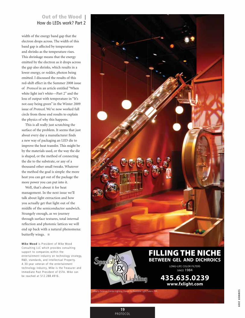
Liberty Science Center. Lighting Design by Available Light, Salem, MA
. . . it’s the meat in the sandwich that produces the light.“
“
at Santa Barbara) demonstrated a gallium
nitride (GaN) material that was capable of
producing high output blue light. Strangely
enough, although we now have materials
that have the right height band gaps to
generate long wavelength light in the reds
and deep ambers, and others with larger
band gaps that generate short wavelength
light in blues and ultra violet, there is still
a big gap in the middle around the yellows
and greens where no efficient materials
have yet been developed. Ironically, this is
right in the region around 555 nm where
the human eye is most sensitive and LEDs
would be really useful. This gap extends
to around 625 nm as, although amber
LEDS are available, their performance and
stability is poor. Considerable fame and
fortune awaits the researcher who manages
to plug this hole and patent the process! In
the meantime developments in phosphor
assisted LEDs where amber or yellow
phosphors are excited by a deep blue or UV
LED are helping fill the visible gap.
Next time I’ll continue this tale and talk
about how the semiconductor materials
are packaged to control and maximize light
output and the innovation that is going in
to that and heat management. Strangely
enough as we journey through photonic
lattices we will end up back with a natural
phenomena; butterfly wings. ■
Mike Wood i s P res ident o f Mike Wood Consu l t ing LLC which prov ides consu l t ing suppor t to companies wi th in the ente r ta inment indust ry on techno logy s t ra tegy, R&D, s tandards, and In te l lec tua l P roper ty. A 30-year ve te ran o f the ente r ta inment techno logy indust ry, Mike i s the Treasure r and Immediate Pas t P res ident o f ESTA. Mike can be reached at 512.288.4916.
Out of the Wood | How do LEDs work?

16SUMMER 2009
SU
MM
ER
20
09
How do LEDs work? Part 2Understanding the challenges of heat management
Out of the WoodBY MIKE WOOD
IN THE LAST ISSUE we covered, while hopefully not getting
bogged down too much into the physics, some of the basic
principles of how an LED (Light Emitting Diode) produces
light without glowing red hot or using an arc. We talked about
PN junctions and how the light is produced at that junction as
electrons fall from a high energy level down into a lower energy
one and give off that excess energy as a photon of light. However
producing the light is only a very small part of the tale. Getting
that light out and keeping everything cool and comfortable is of
equal—if not more—importance to producing a useful and usable
light source.
I’ll continue this tale and talk about how the semiconductor
materials are packaged to control heat and maximize light output
and the innovation that is going in to that and heat management.
Although in almost every other way an LED is significantly
different from other more familiar light sources, it shares one
fundamental problem with all the others—too much heat.
Heat management is the single biggest problem we have to deal
with when designing a luminaire to use LED light sources. The
perception might be that, because it’s a semiconductor-based
emitter with high efficacy—a high ability to turn energy into
light with a perceived brightness—heat emission is minimal.
Unfortunately that’s not at all true and heat is still a huge problem.
Current efficacies of commercially available LEDs are approaching
100 lum/W for a white LED and perhaps 80 lum/W for single
colors such as green. Those figures sound and are very good
compared to conventional light sources, but still fall a long way
short of what is theoretically possible.
The maximum possible efficiency for a white source is not an
easy number to pin down as it depends on the color temperature
we want as well as the CRI we are prepared to live with, and you
also have to integrate under the photopic curve to allow for the
eye’s different sensitivity to different colors. However, very roughly,
the maximum possible efficacy is about 260 lum/W for 3200 K
black-body white light. Let’s compare that with the efficacies of
real light sources. The very best incandescent lamps have efficacies
approaching 30 lum/W which is about 11% of this theoretical
maximum. (Luminous efficiency is usually expressed as a percentage
of the theoretical maximum. For our incandescent lamp that is 30 /
260 = 11%.)
On the same basis a 100 lum/W white LED will be about 38%
efficient—much better than the incandescent, but it still means
that over 60% of the supplied energy is being emitted as heat. Our
green LED is even worse; the theoretical maximum output for a
monochromatic green light right at the peak of the photopic curve
at 555 nm is 683 lum/W so our 80 lum/W green LED is actually less
than 10% efficient and very similar to our incandescent lamp with
90% of the supplied energy appearing as heat.
Heat is always where energy ends up. It’s the end of the line
for energy and a fundamental of thermodynamics. You can
pretty much paraphrase the first two laws of thermodynamics as
“Everything you do eventually ends up as heat and there’s not
a darn thing you can do about it.” Or, as Sting and The Police
almost put it:
Every breath you take
And every move you make
Every bond you break, every step you take
. . . ends up as heat!
Everything you do eventually ends up as heat and there’s not a darn thing you can do about it.“
“
17PROTOCOL
SU
MM
ER
20
09
Out of the Wood | How do LEDs work? Part 2
Efficient thermal management of the luminaire and the enclosed
LED package present the most fundamental design challenges for
anyone involved in LED product design and decisions made here
affect the efficiencies and success of the entire project.
Apart from I2R losses in leads and connections, the majority of
the heat generated is produced within the junction of the LED,
just where it’s the most difficult to get out. As is often the case
with engineering design there are two conflicting requirements: to
maximize light output we want to leave the LED die as open and
unrestricted as possible, whereas for maximal heat transfer we want
to surround and connect it with efficient thermal conductors. We
clearly need to leave the top of the device as open as possible for
light to exit so, in most cases, heat only has one path out of the
LED; via a heat slug to the bottom of the LED package to the PCB.
The top of the package is sealed, often with optical materials that
are poor thermal conductors, trapping the LED die itself in a sealed
package like a small oven.
An awful lot of R&D and design goes in to reconciling these
conflicts to produce the brightest and most efficient products.
Fundamentally the goal is to get the heat out of the bottom of the
package as rapidly as you can while simultaneously collecting and
controlling the light output from the top.
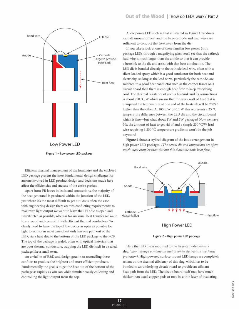
A low power LED such as that illustrated in Figure 1 produces
a small amount of heat and the large cathode and lead wires are
sufficient to conduct that heat away from the die.
If you take a look at one of these familiar low power 5mm
package LEDs through a magnifying glass you’ll see that the cathode
lead wire is much larger than the anode so that it can provide
a heatsink to the die and assist with that heat conduction. The
LED die is bonded directly to the cathode lead wire, often with a
silver-loaded epoxy which is a good conductor for both heat and
electricity. As long as the lead wires, particularly the cathode, are
soldered to a good heat conductor such as the copper traces on a
circuit board then there is enough heat flow to keep everything
cool. The thermal resistance of such a heatsink and its connections
is about 250 °C/W which means that for every watt of heat that is
dissipated the temperature at one end of the heatsink will be 250°C
higher than the other. At 100 mW or 0.1 W this represents a 25 °C
temperature difference between the LED die and the circuit board
which is fine—but what about 1W and 5W packages? Now we have
50x the amount of heat to get rid of and a simple 250 °C/W lead
wire requiring 1,250 °C temperature gradients won’t do the job
anymore!
Figure 2 shows a stylized diagram of the basic arrangement in
high power LED packages. (The actual die and connections are often
much more complex than this but this shows the basic heat flow.)
Figure 2 – High power LED package
Here the LED die is mounted to the large cathode heatsink
slug (often through a submount that provides electrostatic discharge
protection). High powered surface-mount LED lamps are completely
reliant on the thermal efficiency of this slug, which has to be
bonded to an underlying circuit board to provide an efficient
heat path from the LED. The circuit board itself may have much
thicker than usual copper pads or may be a thin layer of insulating
Figure 1 – Low power LED package

18SUMMER 2009
SU
MM
ER
20
09
epoxy material on top of an aluminum core; it could even be
some composite material such as a heat conducting ceramic
or other esoteric material. Whatever it is, the goal is minimal
thermal resistance while providing a stable substrate for providing
the electrical connections and mounting the package. The heat
dissipation problem doesn’t stop there though; the heat has to be
led away from the circuit board, usually to a connected heatsink.
We are also starting to see real innovation in what happens next
to that heat energy. We need to get it as far away from our LEDs
as we can. The easiest way to do that is through fans, but those
are anathema to our industry. (Anathema is the perfect word—it’s
defined as “a person or thing accursed or consigned to damnation or
destruction,” which I think describes pretty well the reaction of many
lighting designers to noisy fans!) That means either large passive
heatsinks or some other quieter method of active cooling. A couple
of manufacturers have experimented with Peltier cooling systems,
which are semiconductor heat pumps, while others are looking
at heat pipes such as those used in many computers to keep the
main processor chilled. Figure 3 shows the basic principle of a heat
pipe—it uses exactly the same principle as a refrigerator or HVAC
system where a volatile fluid is evaporated taking up heat from its
surroundings to do so and then condenses back to a liquid again
in another location giving up that heat. In the case of a heat pipe
there is no pump or compressor involved to move the liquid and it
instead relies upon capillary action in a wick or pipe to move the
fluid. The heat comes from the LED slug and is transferred via the
evaporated vapor to a large heatsink where it condenses back to a
liquid again. I expect we’ll see many other innovations in this area
as time goes on—should be interesting!
Figure 3 – Heat pipe
But why the big fuss about heat in
the first place? When an incandescent or
discharge lamp runs too hot the result is
usually a shortened life, but the effects
of too much heat in an LED system
can be subtler and more insidious. As
well as also losing life with increased
temperature, the quantum efficiency of
LEDs is temperature sensitive so that,
as the temperature rises, the output
drops. The effect is relatively small with
blue and green LEDs, but can be very
significant with ambers and reds. In fact
an amber LED can easily lose 50% or
more of its initial output as it warms up
from room temperature to an operating
point around 80°C. Just to compound
the problem the color of the LED moves
with temperature as well. If you recall
from the last article the wavelength of
the light emitted is determined by the
A thing accursed or consigned to damnation or destruction . . .“
“
Toll Free: 888-577-3876
JS-ICONJS-ICON Series dimmer and solid-state relay racks are the ultimatevalue in professional dimming!Advanced electronics create the “greenest” dimmer rack available and compliance with the International Energy Agency’s “One Watt Initiative” for standby power consumption. Unique “lamp warming” feature
Powerful user interface allows for ease of advanced feature usage. Several models permit a wide range of applications. Up to 10 year warranty available!
TM
Out of the Wood | How do LEDs work? Part 2
19PROTOCOL
SU
MM
ER
20
09
width of the energy band gap that the
electron drops across. The width of this
band gap is affected by temperature
and shrinks as the temperature rises.
This shrinkage means that the energy
emitted by the electron as it drops across
the gap also shrinks, which results in a
lower energy, or redder, photon being
emitted. I discussed the results of this
red-shift effect in the Summer 2008 issue
of Protocol in an article entitled “When
white light isn’t white—Part 2” and the
loss of output with temperature in “It’s
not easy being green” in the Winter 2009
issue of Protocol. We’ve now worked full
circle from those end results to explain
the physics of why this happens.
This is all really just scratching the
surface of the problem. It seems that just
about every day a manufacturer finds
a new way of packaging an LED die to
improve the heat transfer. This might be
by the materials used, or the way the die
is shaped, or the method of connecting
the die to the substrate, or any of a
thousand other small tweaks. Whatever
the method the goal is simple: the more
heat you can get out of the package the
more power you can put into it.
Well, that’s about it for heat
management. In the next issue we’ll
talk about light extraction and how
you actually get that light out of the
middle of the semiconductor sandwich.
Strangely enough, as we journey
through surface textures, total internal
reflection and photonic lattices we will
end up back with a natural phenomena:
butterfly wings.
Mike Wood i s P res ident o f Mike Wood Consu l t ing LLC which prov ides consu l t ing suppor t to companies wi th in the ente r ta inment indust ry on techno logy s t ra tegy, R&D, s tandards, and In te l lec tua l P roper ty. A 30-year ve te ran o f the ente r ta inment techno logy indust ry, Mike i s the Treasure r and Immediate Pas t P res ident o f ESTA. Mike can be reached at 512.288.4916.
Out of the Wood | How do LEDs work? Part 2
20FAll 2009
FALL
20
09
How do LEDs work? Part 3A look at the science and physics behind leDs
Out of the WoodbY MIKE WOOD
In the last tWo Issues we covered the basic principles of
operation of how an led (light emitting diode) produces light
and how, even though the mechanism for producing light is
completely different from other sources, some things never change,
and heat is still public enemy number one. In this article I want
to discuss how that light finally gets out of the led die and the
problems—and solutions—associated with that process.
as we discussed in the earlier articles, the light in an led isn’t
produced on the surface of the led die. Instead, it’s emitted from
the area where the P and n layers meet called the junction. this is
very inconvenient, as the junction is right in the middle of the die,
a bit like the meat in the sandwich, so how does the light actually
get out of there? firstly, it seems pretty clear that at least one of the
layers making up the semiconductor has to be transparent to the
wavelengths of light that the led is producing! Without that, all
you would have is a rather small heater. so now the light has to
get out of the semiconductor, but that doesn’t sound too bad if
it’s transparent does it? however, there’s a huge “gotcha”
that can reduce the amount of light that escapes the die down
to a tiny percentage of the original. that problem is tIr, total
Internal reflection.
total internal reflectionsometimes tIr is our friend, sometimes it’s our foe. let’s start off
by explaining what it is. total internal reflection is what can happen
when light passes from an area of higher refractive index to one of a
lower refractive index, such as when light passes from glass to air or
water to air. If that light hits the boundary between the two media
at right angles to the boundary, then it passes straight through and
all is fine. as the angle between the light beam and the boundary
increases the exiting light will be bent by refraction through a
greater and greater angle until eventually it’s bent so much that it
refracts parallel with the boundary. any increase in angle beyond
that will result in the light being reflected back from the boundary
as if it were a mirror. a very familiar example of this is the effect
you get when snorkeling or scuba diving and you try and look up
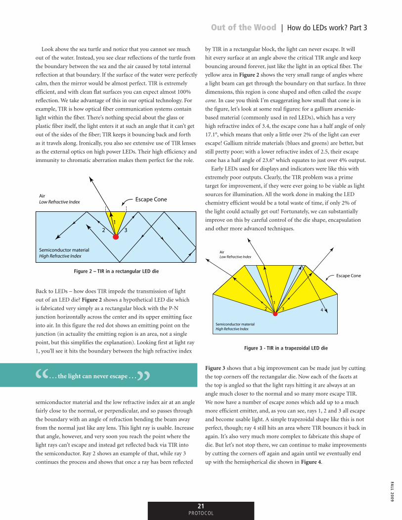
and out of the water as in Figure 1.
Figure 1 – Total Internal Reflection underwater(This is a photograph from a recent vacation in Mexico—
little did the sea turtle know that he was going to be used as an example of TIR.)
. . . there’s a huge ‘Gotcha’ which can reduce the amount of light that escapes the die down to a tiny percentage of the original.“
“
21protocol
FALL 2
00
9
Out of the Wood | How do LEDs work? Part 3
. . . the light can never escape . . .“
“
look above the sea turtle and notice that you cannot see much
out of the water. Instead, you see clear reflections of the turtle from
the boundary between the sea and the air caused by total internal
reflection at that boundary. If the surface of the water were perfectly
calm, then the mirror would be almost perfect. tIr is extremely
efficient, and with clean flat surfaces you can expect almost 100%
reflection. We take advantage of this in our optical technology. for
example, tIr is how optical fiber communication systems contain
light within the fiber. there’s nothing special about the glass or
plastic fiber itself, the light enters it at such an angle that it can’t get
out of the sides of the fiber; tIr keeps it bouncing back and forth
as it travels along. Ironically, you also see extensive use of tIr lenses
as the external optics on high power leds. their high efficiency and
immunity to chromatic aberration makes them perfect for the role.
Figure 2 – TIR in a rectangular LED die
Back to leds – how does tIr impede the transmission of light
out of an led die? Figure 2 shows a hypothetical led die which
is fabricated very simply as a rectangular block with the P-n
junction horizontally across the center and its upper emitting face
into air. In this figure the red dot shows an emitting point on the
junction (in actuality the emitting region is an area, not a single
point, but this simplifies the explanation). looking first at light ray
1, you’ll see it hits the boundary between the high refractive index
semiconductor material and the low refractive index air at an angle
fairly close to the normal, or perpendicular, and so passes through
the boundary with an angle of refraction bending the beam away
from the normal just like any lens. this light ray is usable. Increase
that angle, however, and very soon you reach the point where the
light rays can’t escape and instead get reflected back via tIr into
the semiconductor. ray 2 shows an example of that, while ray 3
continues the process and shows that once a ray has been reflected
by tIr in a rectangular block, the light can never escape. It will
hit every surface at an angle above the critical tIr angle and keep
bouncing around forever, just like the light in an optical fiber. the
yellow area in Figure 2 shows the very small range of angles where
a light beam can get through the boundary on that surface. In three
dimensions, this region is cone shaped and often called the escape
cone. In case you think I’m exaggerating how small that cone is in
the figure, let’s look at some real figures: for a gallium arsenide-
based material (commonly used in red leds), which has a very
high refractive index of 3.4, the escape cone has a half angle of only
17.1°, which means that only a little over 2% of the light can ever
escape! gallium nitride materials (blues and greens) are better, but
still pretty poor; with a lower refractive index of 2.5, their escape
cone has a half angle of 23.6° which equates to just over 4% output.
early leds used for displays and indicators were like this with
extremely poor outputs. clearly, the tIr problem was a prime
target for improvement, if they were ever going to be viable as light
sources for illumination. all the work done in making the led
chemistry efficient would be a total waste of time, if only 2% of
the light could actually get out! fortunately, we can substantially
improve on this by careful control of the die shape, encapsulation
and other more advanced techniques.
Figure 3 - TIR in a trapezoidal LED die
Figure 3 shows that a big improvement can be made just by cutting
the top corners off the rectangular die. now each of the facets at
the top is angled so that the light rays hitting it are always at an
angle much closer to the normal and so many more escape tIr.
We now have a number of escape zones which add up to a much
more efficient emitter, and, as you can see, rays 1, 2 and 3 all escape
and become usable light. a simple trapezoidal shape like this is not
perfect, though; ray 4 still hits an area where tIr bounces it back in
again. It’s also very much more complex to fabricate this shape of
die. But let’s not stop there, we can continue to make improvements
by cutting the corners off again and again until we eventually end
up with the hemispherical die shown in Figure 4.
12 3
Escape Cone
Semiconductor materialHigh Refractive Index
AirLow Refractive Index
12 3 4
Escape Cone
Semiconductor materialHigh Refractive Index
AirLow Refractive Index

22FAll 2009
FALL
20
09
Out of the Wood | How do LEDs work? Part 3
Figure 4 - TIR in a hemispherical LED die
now all the light emitted in an upwards direction will hit the
boundary at a normal angle and so will all escape with no tIr at
all. unfortunately, fabricating dies in hemispherical shapes would
be extremely difficult and expensive. semiconductor manufacture
is essentially a laminar process, where you build up a series of flat
layers by deposition or remove them by etching back, which doesn’t
suit these complex three-dimensional shapes. Is there nothing else
that can be done?
EncapsulationI’m sure you’ve noticed that many led dies have a covering of
transparent epoxy or silicon on top of the die. you may have
thought this encapsulation was to protect the die. It does indeed
provide protection, but it also can help with reducing tIr losses.
Figure 5 - TIR with epoxy encapsulation of the LED die
12 3
Escape Cone
Semiconductor materialHigh Refractive Index
AirLow Refractive Index
12 3
Escape Cone
Semiconductor materialHigh Refractive Index
AirLow Refractive Index
EpoxyMid Refractive Index

23protocol
FALL 2
00
9
Out of the Wood | How do LEDs work? Part 3
Figure 5 shows the same simple rectangular led die shown in
Figure 2, but with a hemispherical cap of an epoxy encapsulant on
top of it. this encapsulant is chosen to have a refractive index that
is between those of the semiconductor and the surrounding air.
so, although we’ve doubled the number of boundaries from one to
two, each one has a smaller difference in refractive index, and thus
a larger escape cone. this is particularly helpful at the boundary
between the semiconductor and the encapsulant. a simple
encapsulant like this can improve the light extraction efficiency by
a factor of 2x, taking our original 2% up to 4%. this is still not too
good for light output, but is inexpensive and sufficient for many
indicator style leds.
led manufacturers have invested significant r&d dollars into
improving light extraction figures, and much of the light output
increase we’ve seen in the last few years from high power leds has
come about because of this work. different shapes and sizes of led
dies, different surface finishes, surface gratings using diffraction
rather than refraction, anti-reflection coatings, and different
encapsulants can all help. you may have seen dies that are inverted
truncated pyramids, some described as flip chips and other strange
names. these are all means of improving the light extraction.
photonic latticesone of the more recent improvements in light extraction has come
from the inclusion of photonic lattices in the top layers of the
junction. the idea was first proposed in 1987 by eli yablonovitch,
now at the university of california at Berkeley, and has since
spawned r&d efforts worldwide to expand and exploit the concept.
the methods for manufacturing the crystals and the precise modes
of operation are outside our scope (and my understanding!), but
the interesting result is that long, thin, crystalline formations are
embedded in the material, which to some extent act as diffractive
waveguides and improve light extraction by redirecting and
diffracting light out of the semiconductor.
Figure 6 shows a very simplified representation of the
layout. the photonic lattice crystals in the upper part of the
semiconductor sandwich tend to redirect the light along their
length and thus much closer to the normal of the semiconductor/
air boundary, avoiding tIr reflections back into the material.
the very latest developments in this technology in real products
from companies like luminus devices and Philips lumileds are
achieving light extraction efficiencies in excess of 70%—a far cry
from the 2% efficiencies we started at!
In the last article I promised you butterfly wings—but how do
we get from a discussion on extraction efficiencies of leds to the
wings of lepidoptera? research in recent years has shown that

22FALL 2009
FALL
20
09
It’s as EASY 1. Rack ’em up2. Roll ’em out3. Plug ’em in
Custom con�gure online at: www.LexProducts.com
Roadworthy Construction• Extruded aluminum frame with high impact plastic panels provide a lightweight, extremely durable rolling rack
• Resistant to corrosion, scratching and denting
Innovative Design• Recessed cups on top panel for stacking
• “Snap-in” latches on front and back panels for quick access
Custom Configuration• DX digital dimming capability
• State-of-the-art laser engraving on top and side panels also available
Rolling Distribution RacksPowerRACK™
Lex Products Corporation401 Shippan AvenueStamford, CT 06902203.363.3738 203.363.3742 Fax
Lex West1847 Sheldon StreetSun Valley, CA 91352818.768.4474818.768.4040 Fax
C
M
Y
CM
MY
CY
CMY
K
Lex_protocol_winter_08 pressready.pdf 12/11/2008 4:51:20 PM
the iridescent colors of various animals, including beetles and
butterflies, are very often due to photonic crystals rather than
any pigments. the size, shape, and pitch of these crystals, and
their bumps and holes act to selectively absorb or reflect different
wavelengths of light, and thus appear in different colors even
though the crystals themselves are actually colorless. additionally,
because these photonic crystal arrays behave differently at
different angles, just like the dichroic filters we are more familiar
with, the resultant colors often iridesce and shift in a striking and
alluring (at least to other butterflies) manner.
the science and physics behind leDs is a fascinating and
complex topic, and we’ve really only scratched the surface in
this short series. It’s also a rapidly changing topic, with regular
significant breakthroughs in many areas. one thing’s for sure: it’s a
topic we’ll be returning to. n
Bibliography:
highly recommended but very technical book concerning the detailed
operation of leDs:
‘light-emitting Diodes’ by e. Fred schubert published by Cambridge
university Press (2nd edition)
Mike Wood i s p res ident o f Mike Wood consu l t ing LLc which prov ides consu l t ing suppor t to companies wi th in the ente r ta inment indust ry on techno logy s t ra tegy, R&D, s tandards, and In te l lec tua l p roper ty. A 30-year ve te ran o f the ente r ta inment techno logy indust ry, Mike i s the Treasure r and Immediate pas t p res ident o f ESTA. Mike can be reached at 512.288.4916.
12 3 Escape Cone
Semiconductor materialHigh Refractive Index
AirLow Refractive Index
Photonic LatticeCrystal
Figure 6 – Photonic lattice structure
Out of the Wood | How do LEDs work? Part 3