Embed Size (px)
Citation preview
How a detector works ?
Sven Herrmann
LCLS/SSRL users meeting – detector workshop
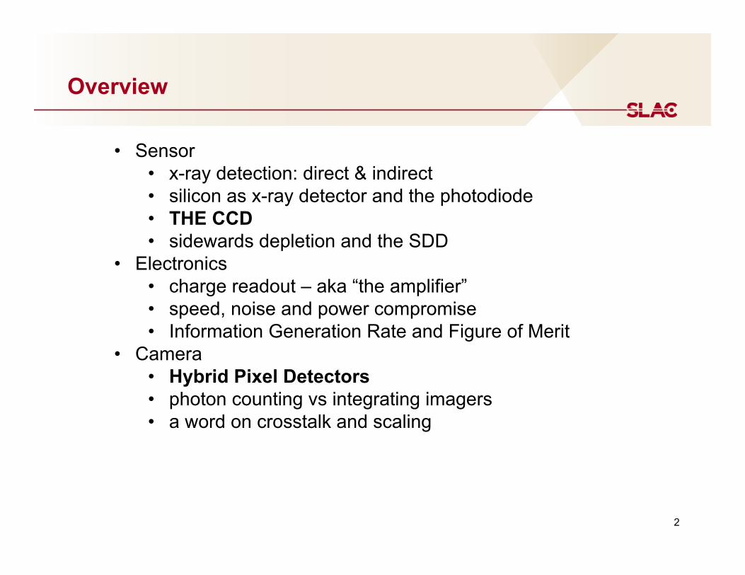
Overview
• Sensor • x-ray detection: direct & indirect • silicon as x-ray detector and the photodiode • THE CCD • sidewards depletion and the SDD
• Electronics • charge readout – aka “the amplifier” • speed, noise and power compromise • Information Generation Rate and Figure of Merit
• Camera • Hybrid Pixel Detectors • photon counting vs integrating imagers • a word on crosstalk and scaling
2
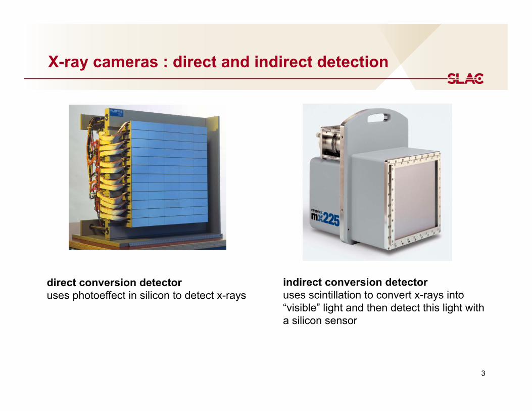
X-ray cameras : direct and indirect detection
direct conversion detector uses photoeffect in silicon to detect x-rays
indirect conversion detector uses scintillation to convert x-rays into “visible” light and then detect this light with a silicon sensor
3
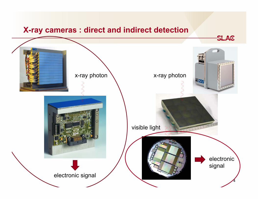
X-ray cameras : direct and indirect detection
electronic signal
electronic signal
x-ray photon x-ray photon
visible light
4
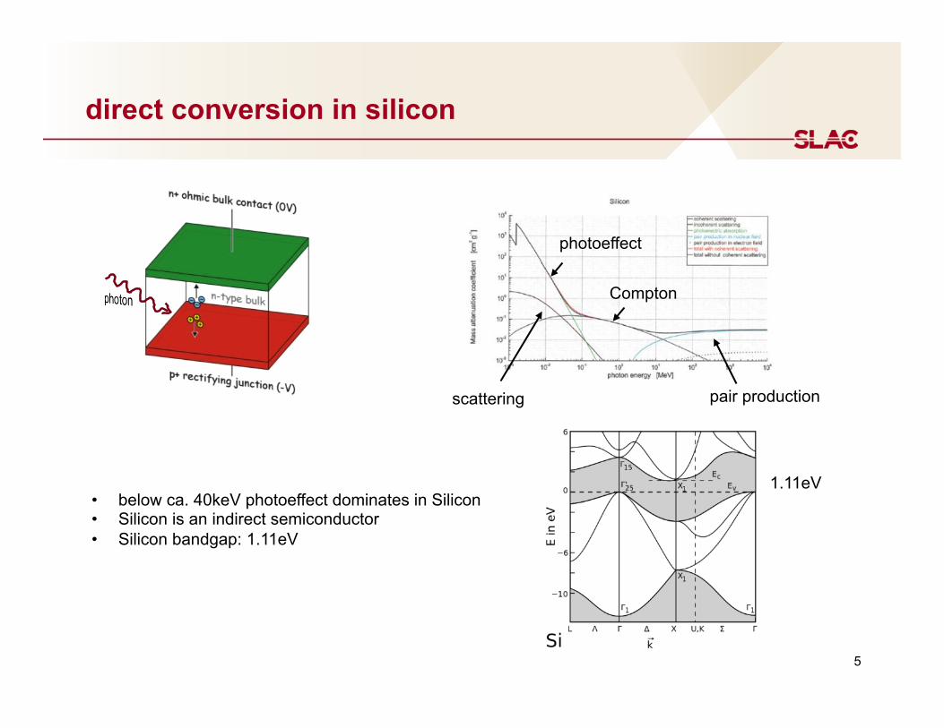
direct conversion in silicon
• below ca. 40keV photoeffect dominates in Silicon • Silicon is an indirect semiconductor • Silicon bandgap: 1.11eV
1.11eV
photoeffect
Compton
pair production scattering
5
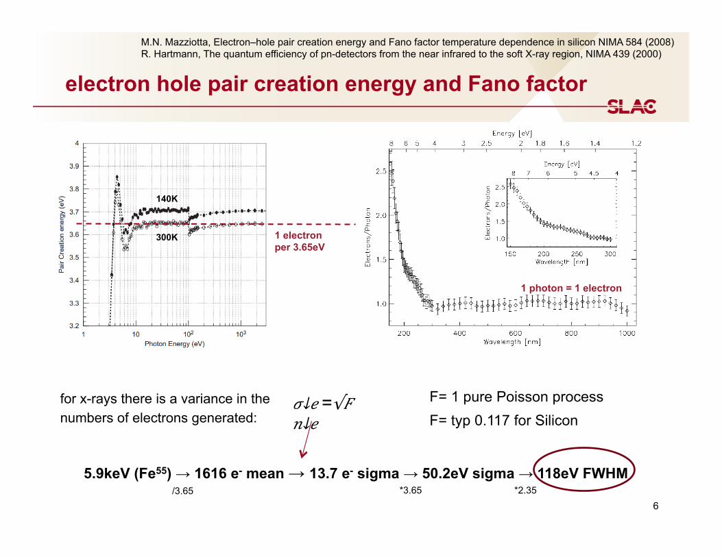
electron hole pair creation energy and Fano factor
140K
300K 1 electron per 3.65eV
1 photon = 1 electron
"↓$ =√'(↓$
F= 1 pure Poisson process F= typ 0.117 for Silicon
for x-rays there is a variance in the numbers of electrons generated:
M.N. Mazziotta, Electron–hole pair creation energy and Fano factor temperature dependence in silicon NIMA 584 (2008) R. Hartmann, The quantum efficiency of pn-detectors from the near infrared to the soft X-ray region, NIMA 439 (2000)
5.9keV (Fe55) → 1616 e- mean → 13.7 e- sigma → 50.2eV sigma → 118eV FWHM /3.65 *3.65 *2.35
6
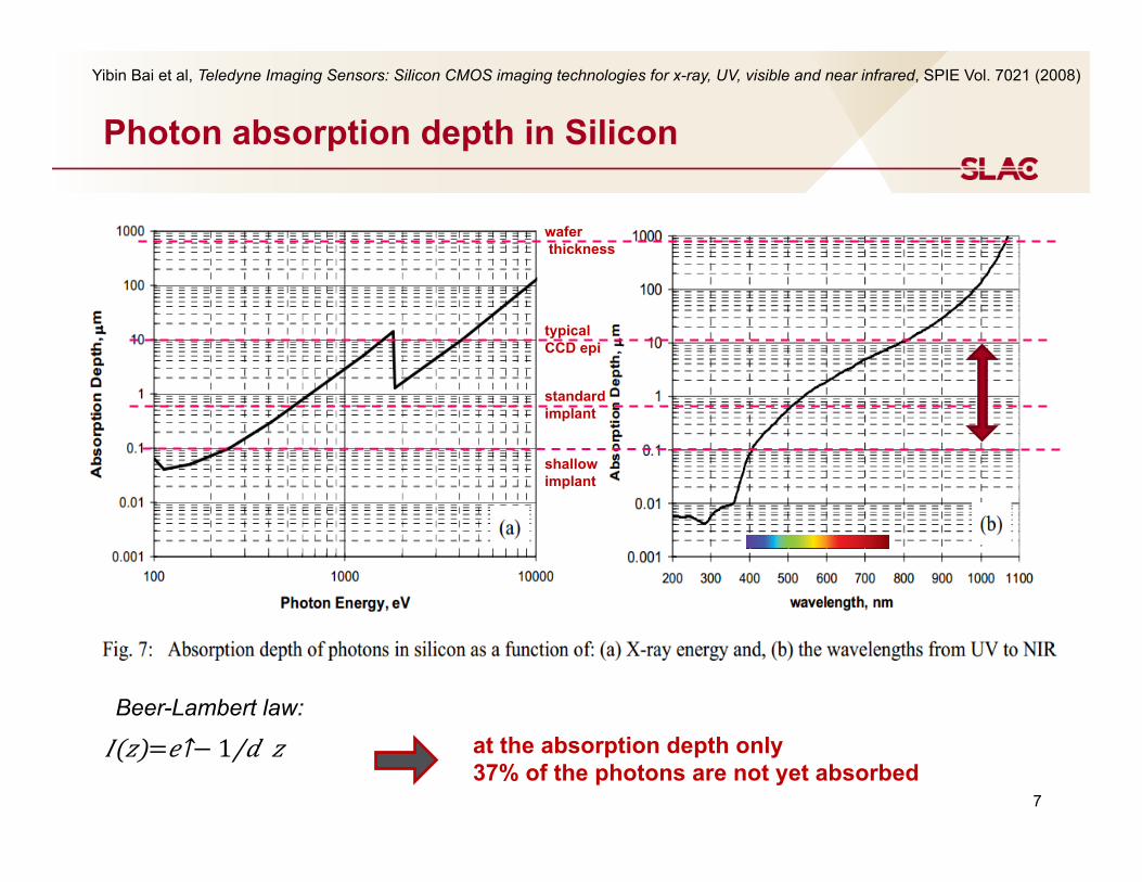
Photon absorption depth in Silicon
Yibin Bai et al, Teledyne Imaging Sensors: Silicon CMOS imaging technologies for x-ray, UV, visible and near infrared, SPIE Vol. 7021 (2008)
)(+)= $↑− 1// + at the absorption depth only 37% of the photons are not yet absorbed
Beer-Lambert law:
wafer thickness
typical CCD epi
standard implant
shallow implant
7
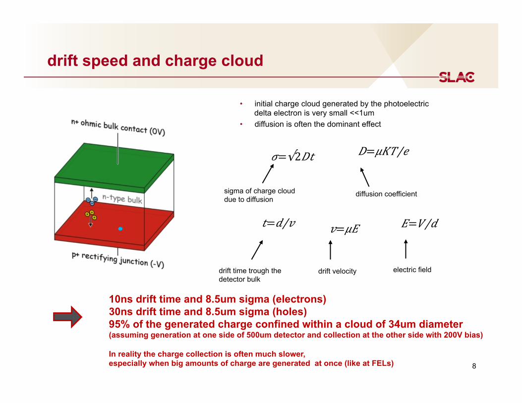
drift speed and charge cloud
• initial charge cloud generated by the photoelectric delta electron is very small <<1um
• diffusion is often the dominant effect
electric field
0=123/$ "=√204
4= //5 5=16 6= 7//
sigma of charge cloud due to diffusion
diffusion coefficient
drift time trough the detector bulk
drift velocity
10ns drift time and 8.5um sigma (electrons) 30ns drift time and 8.5um sigma (holes) 95% of the generated charge confined within a cloud of 34um diameter (assuming generation at one side of 500um detector and collection at the other side with 200V bias) In reality the charge collection is often much slower, especially when big amounts of charge are generated at once (like at FELs) 8
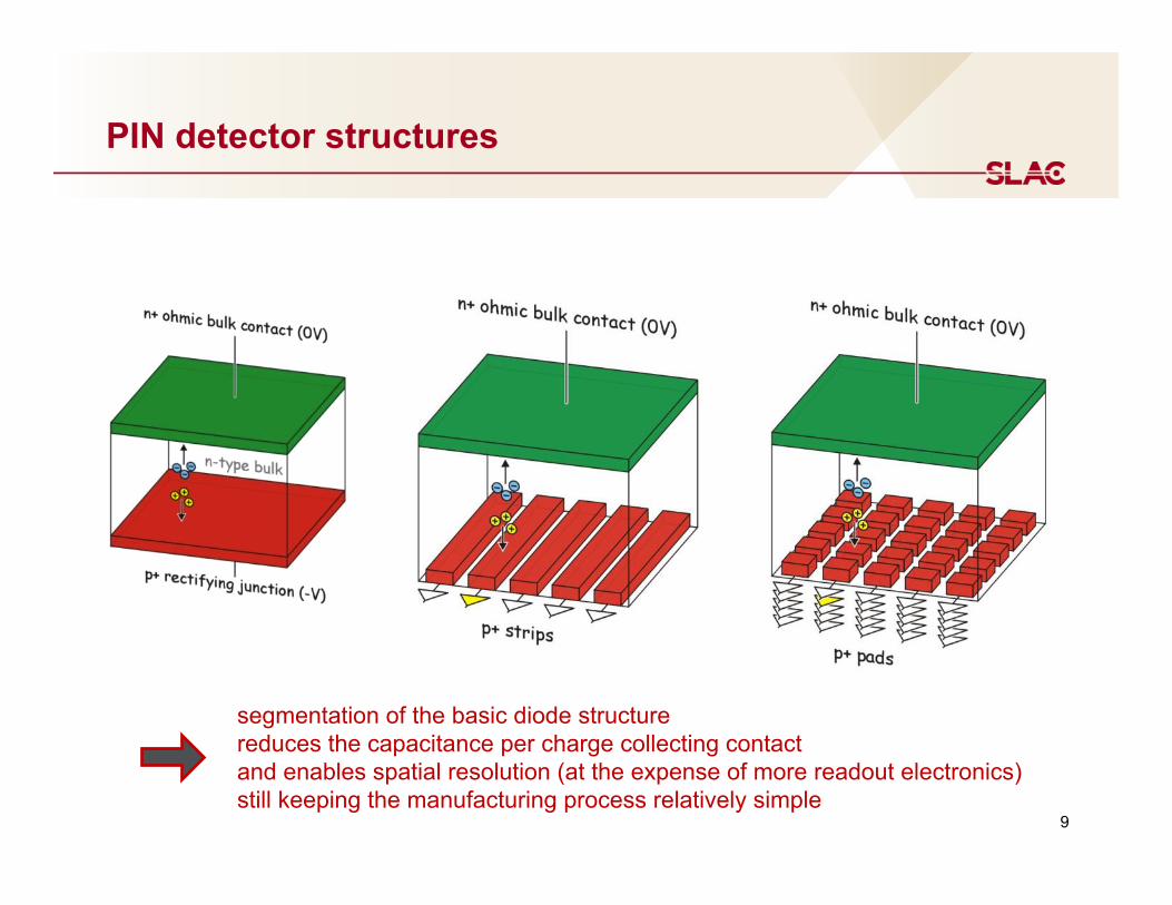
PIN detector structures
segmentation of the basic diode structure reduces the capacitance per charge collecting contact and enables spatial resolution (at the expense of more readout electronics) still keeping the manufacturing process relatively simple
9
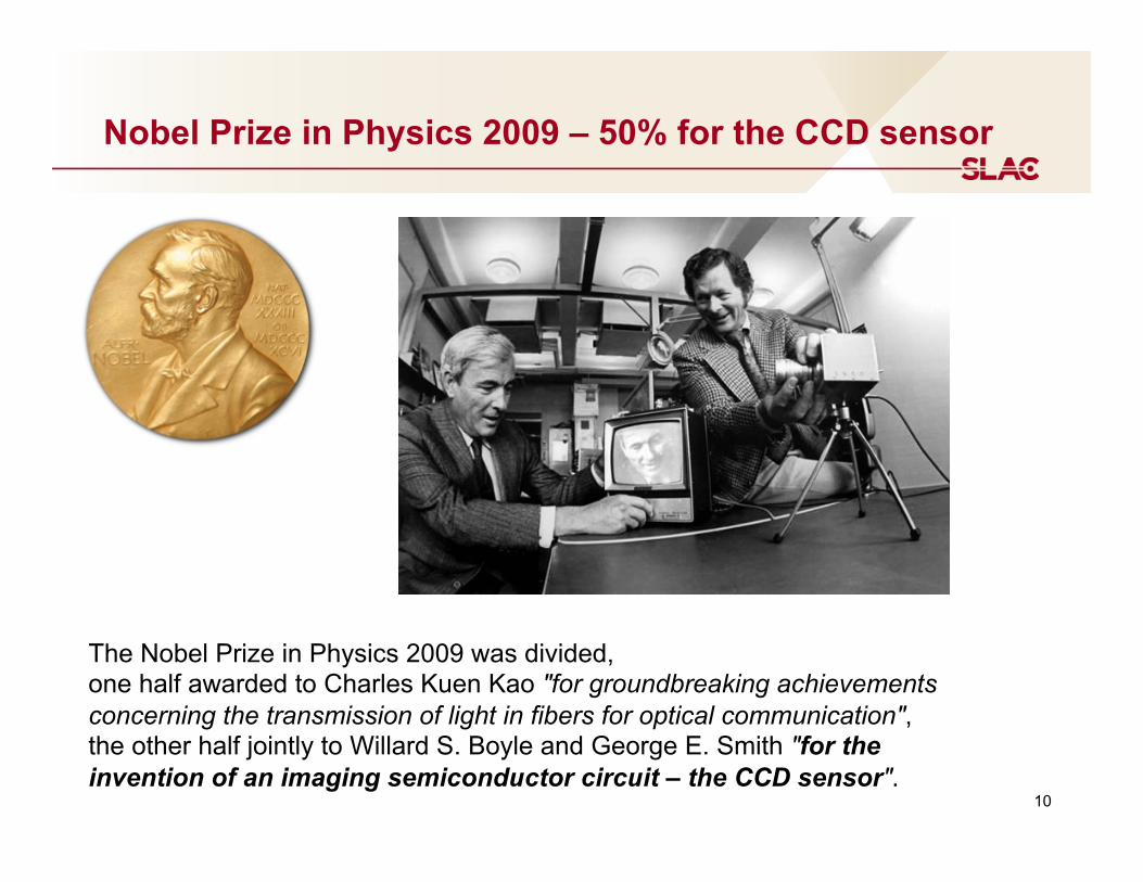
Nobel Prize in Physics 2009 – 50% for the CCD sensor
The Nobel Prize in Physics 2009 was divided, one half awarded to Charles Kuen Kao "for groundbreaking achievements concerning the transmission of light in fibers for optical communication", the other half jointly to Willard S. Boyle and George E. Smith "for the invention of an imaging semiconductor circuit – the CCD sensor".
10
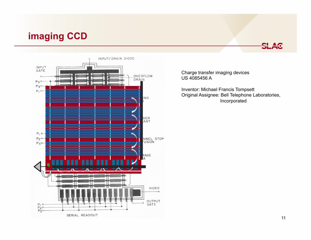
imaging CCD
Charge transfer imaging devices US 4085456 A Inventor: Michael Francis Tompsett Original Assignee: Bell Telephone Laboratories,
Incorporated
11
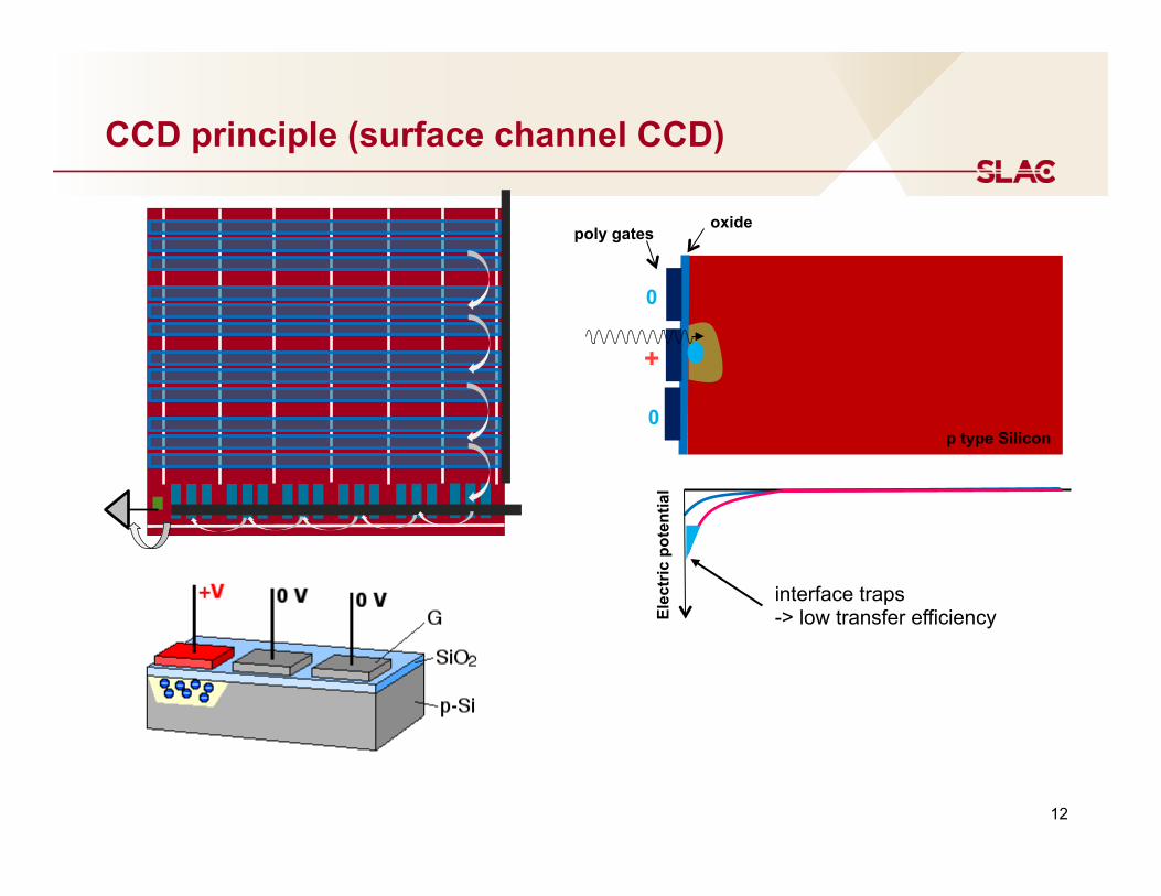
CCD principle (surface channel CCD)
Elec
tric
pot
entia
l
+
0
0 p type Silicon
oxide poly gates
interface traps -> low transfer efficiency
12
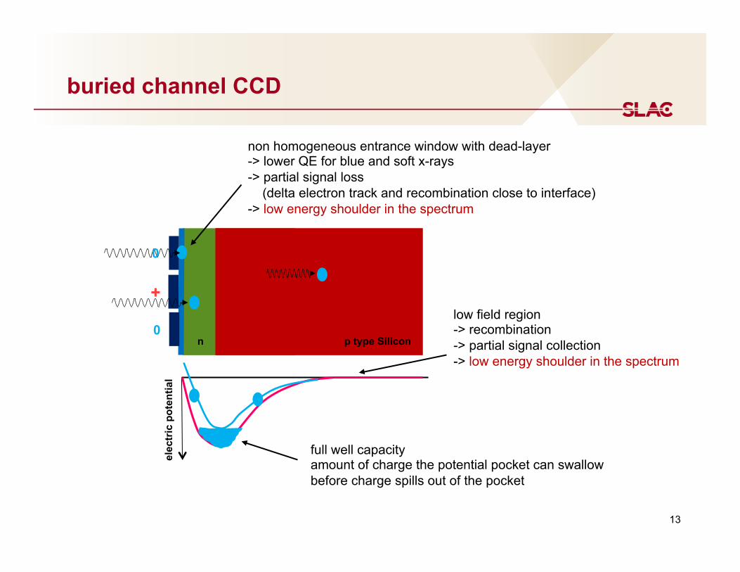
buried channel CCD
low field region -> recombination -> partial signal collection -> low energy shoulder in the spectrum
non homogeneous entrance window with dead-layer -> lower QE for blue and soft x-rays -> partial signal loss (delta electron track and recombination close to interface) -> low energy shoulder in the spectrum
elec
tric
pot
entia
l
+
0
0
full well capacity amount of charge the potential pocket can swallow before charge spills out of the pocket
p type Silicon n
13
0
1000
2000
3000
4000
5000
6000
7000
-‐30 -‐20 -‐10 0 10 20 30 40 50 60 70 80 90 100
norm
alised
cou
nt
histogram bin [ADU]
12keV
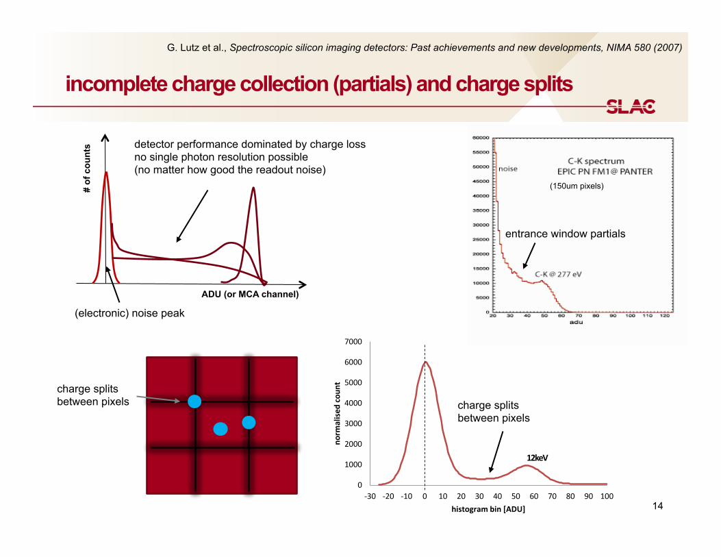
incomplete charge collection (partials) and charge splits
charge splits between pixels
detector performance dominated by charge loss no single photon resolution possible (no matter how good the readout noise)
(electronic) noise peak
ADU (or MCA channel)
# of
cou
nts
G. Lutz et al., Spectroscopic silicon imaging detectors: Past achievements and new developments, NIMA 580 (2007)
entrance window partials
(150um pixels)
charge splits between pixels
14
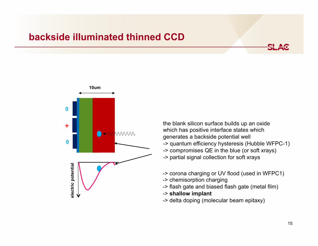
backside illuminated thinned CCD
elec
tric
pot
entia
l
the blank silicon surface builds up an oxide which has positive interface states which generates a backside potential well -> quantum efficiency hysteresis (Hubble WFPC-1) -> compromises QE in the blue (or soft xrays) -> partial signal collection for soft xrays
10um
-> corona charging or UV flood (used in WFPC1) -> chemisorption charging -> flash gate and biased flash gate (metal film) -> shallow implant -> delta doping (molecular beam epitaxy)
+
0
0
15
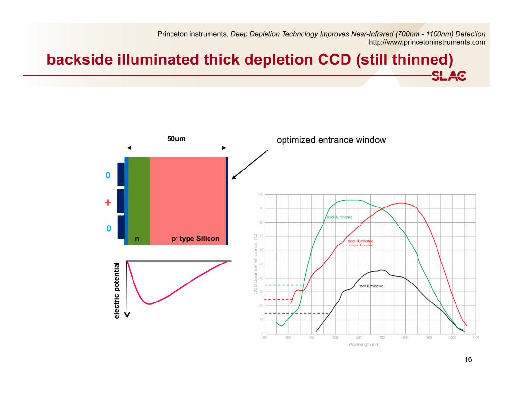
backside illuminated thick depletion CCD (still thinned)
50um
elec
tric
pot
entia
l
optimized entrance window
Princeton instruments, Deep Depletion Technology Improves Near-Infrared (700nm - 1100nm) Detection http://www.princetoninstruments.com
p- type Silicon n
+
0
0
16
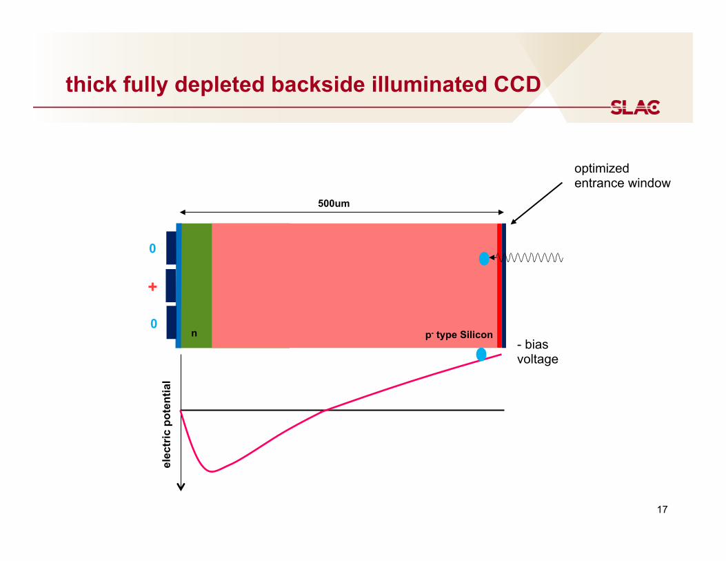
thick fully depleted backside illuminated CCD
elec
tric
pot
entia
l
- bias voltage
optimized entrance window
500um
p- type Silicon n
+
0
0
17
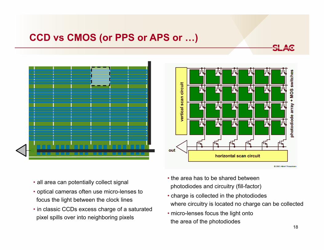
CCD vs CMOS (or PPS or APS or …)
• all area can potentially collect signal • optical cameras often use micro-lenses to focus the light between the clock lines • in classic CCDs excess charge of a saturated pixel spills over into neighboring pixels
• the area has to be shared between photodiodes and circuitry (fill-factor) • charge is collected in the photodiodes where circuitry is located no charge can be collected • micro-lenses focus the light onto the area of the photodiodes
18
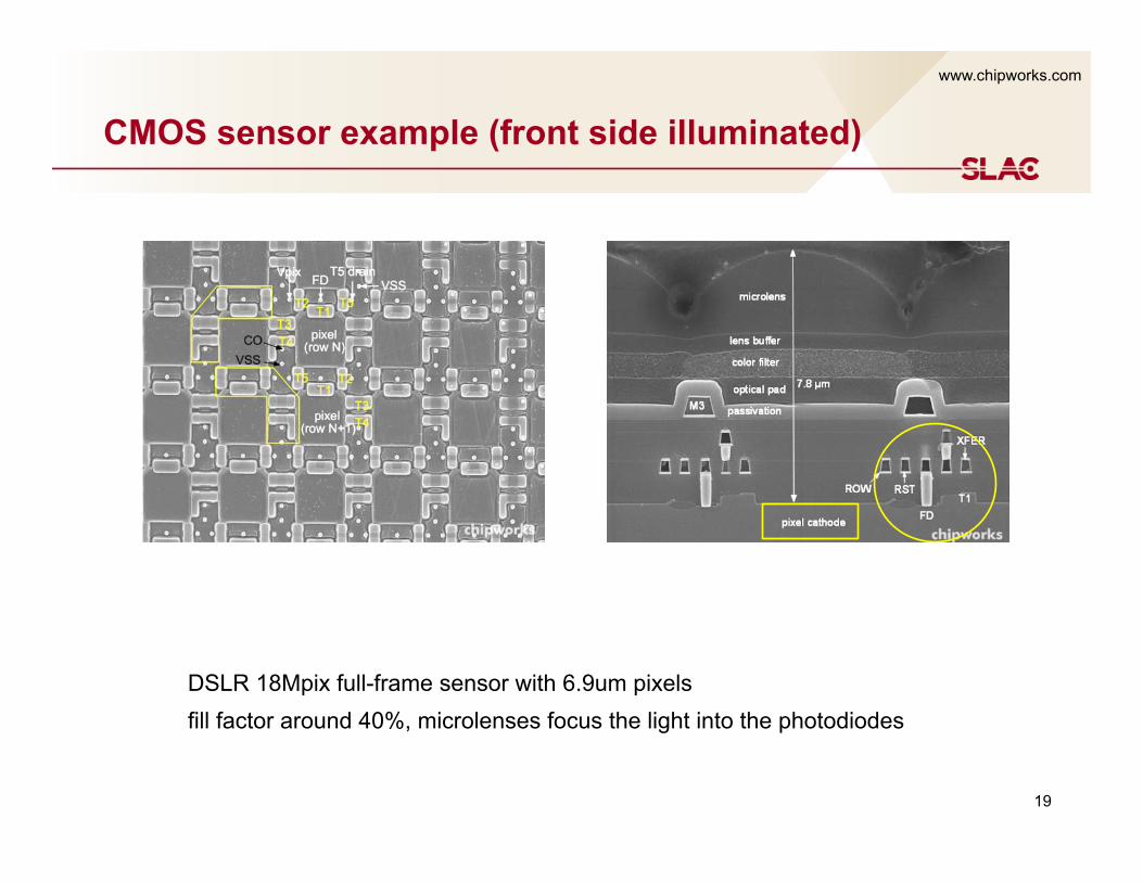
CMOS sensor example (front side illuminated)
DSLR 18Mpix full-frame sensor with 6.9um pixels fill factor around 40%, microlenses focus the light into the photodiodes
www.chipworks.com
19
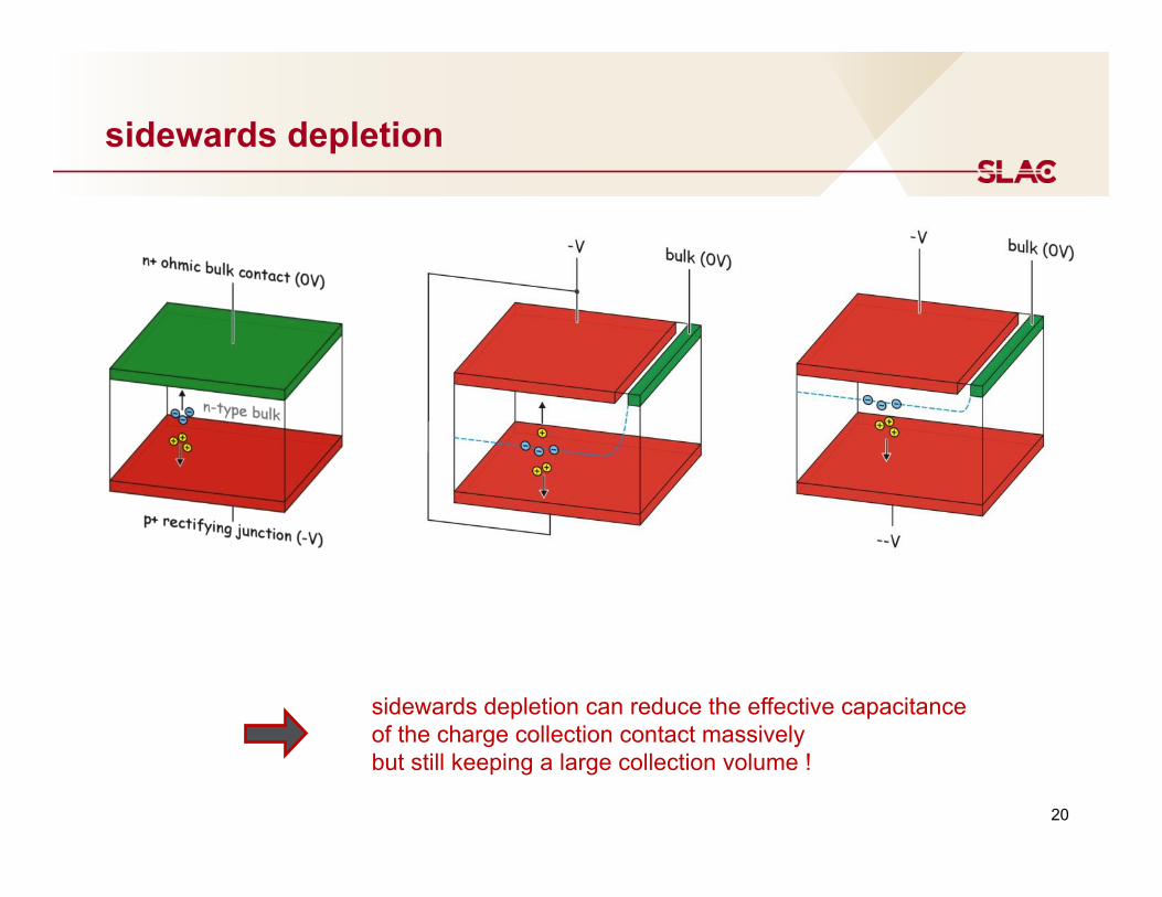
sidewards depletion
sidewards depletion can reduce the effective capacitance of the charge collection contact massively but still keeping a large collection volume !
20
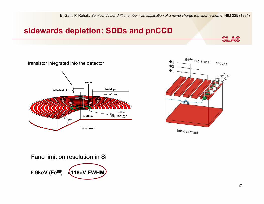
sidewards depletion: SDDs and pnCCD
transistor integrated into the detector
E. Gatti, P. Rehak, Semiconductor drift chamber - an application of a novel charge transport scheme, NIM 225 (1984)
5.9keV (Fe55) → 118eV FWHM
Fano limit on resolution in Si
21
take home bullets from the sensor part
• fully depleted thick silicon (or something with even better stopping power) • backside illumination (homogeneous, better soft x-ray capability) • 100% charge collection
• 100% sensitive volume • shallow (optimized) entrance window
• low leakage current
next: (micro) electronics part
22
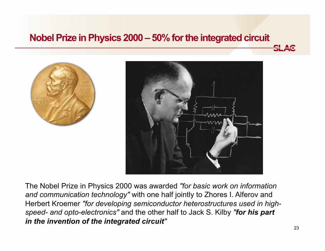
Nobel Prize in Physics 2000 – 50% for the integrated circuit
The Nobel Prize in Physics 2000 was awarded "for basic work on information and communication technology" with one half jointly to Zhores I. Alferov and Herbert Kroemer "for developing semiconductor heterostructures used in high-speed- and opto-electronics" and the other half to Jack S. Kilby "for his part in the invention of the integrated circuit"
23
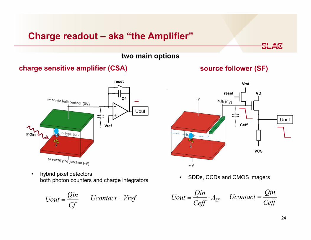
Charge readout – aka “the Amplifier”
Vref Uout
Uout
VD
Vrst
reset
reset
VCS
CfQinUout = SFACeff
QinUout ⋅=
Cf
Ceff
VrefUcontact = CeffQinUcontact =
• hybrid pixel detectors both photon counters and charge integrators • SDDs, CCDs and CMOS imagers
two main options charge sensitive amplifier (CSA) source follower (SF)
24
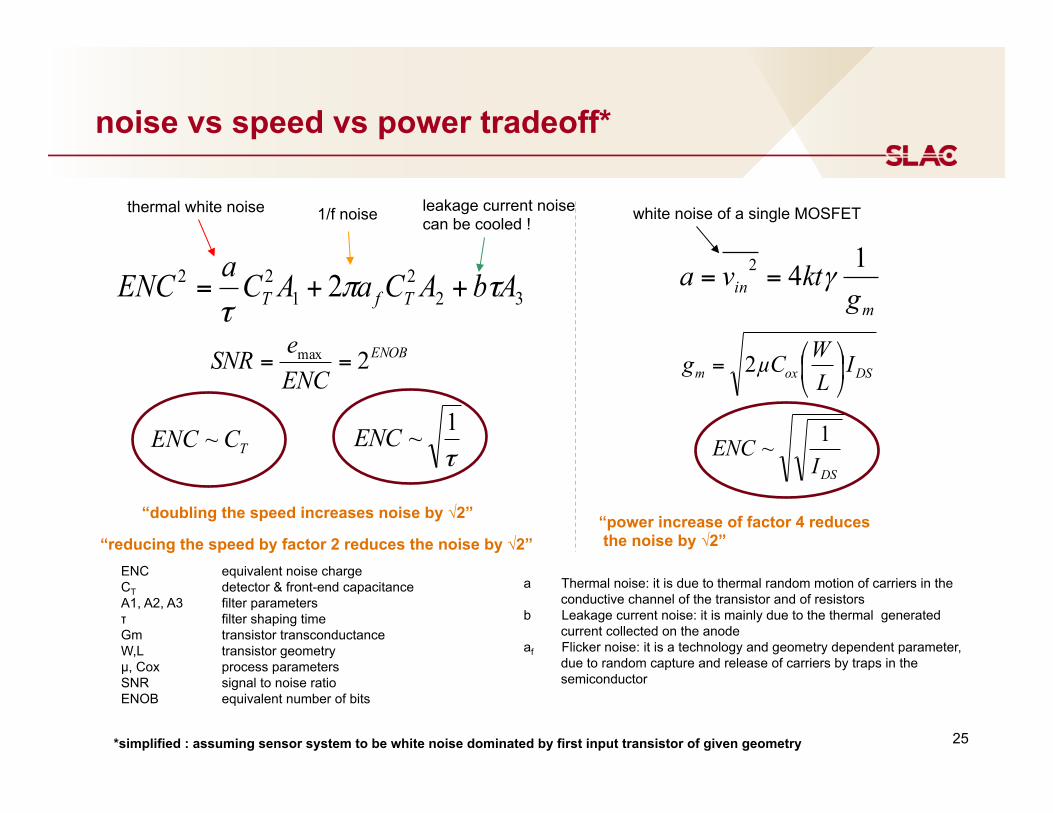
noise vs speed vs power tradeoff*
322
122 2 AbACaACaENC TfT τπ
τ++=
DSoxm ILWµCg ⎟⎠
⎞⎜⎝
⎛= 2
min g
ktva 142 γ==
τ1~ENC
DSIENC 1~
a Thermal noise: it is due to thermal random motion of carriers in the conductive channel of the transistor and of resistors
b Leakage current noise: it is mainly due to the thermal generated current collected on the anode
af Flicker noise: it is a technology and geometry dependent parameter, due to random capture and release of carriers by traps in the semiconductor
ENC equivalent noise charge CT detector & front-end capacitance A1, A2, A3 filter parameters τ filter shaping time Gm transistor transconductance W,L transistor geometry µ, Cox process parameters SNR signal to noise ratio ENOB equivalent number of bits
leakage current noise can be cooled !
thermal white noise
1/f noise
*simplified : assuming sensor system to be white noise dominated by first input transistor of given geometry
“doubling the speed increases noise by √2” “power increase of factor 4 reduces the noise by √2”
white noise of a single MOSFET
ENOB
ENCeSNR 2max ==
“reducing the speed by factor 2 reduces the noise by √2”
TCENC ~
25
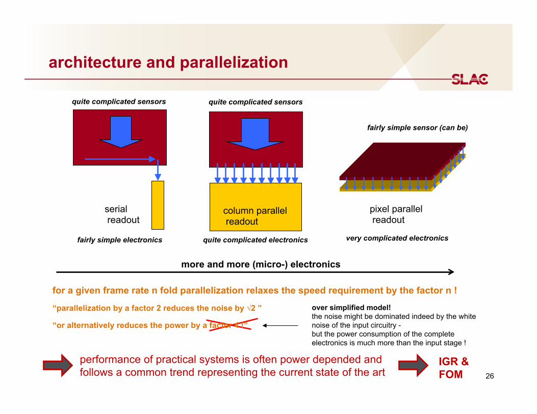
architecture and parallelization
serial readout
“parallelization by a factor 2 reduces the noise by √2 ” over simplified model! the noise might be dominated indeed by the white noise of the input circuitry - but the power consumption of the complete electronics is much more than the input stage !
for a given frame rate n fold parallelization relaxes the speed requirement by the factor n !
“or alternatively reduces the power by a factor 4 !”
more and more (micro-) electronics
column parallel readout
quite complicated sensors
quite complicated electronics
quite complicated sensors
fairly simple electronics
pixel parallel readout
fairly simple sensor (can be)
very complicated electronics
performance of practical systems is often power depended and follows a common trend representing the current state of the art
IGR & FOM 26
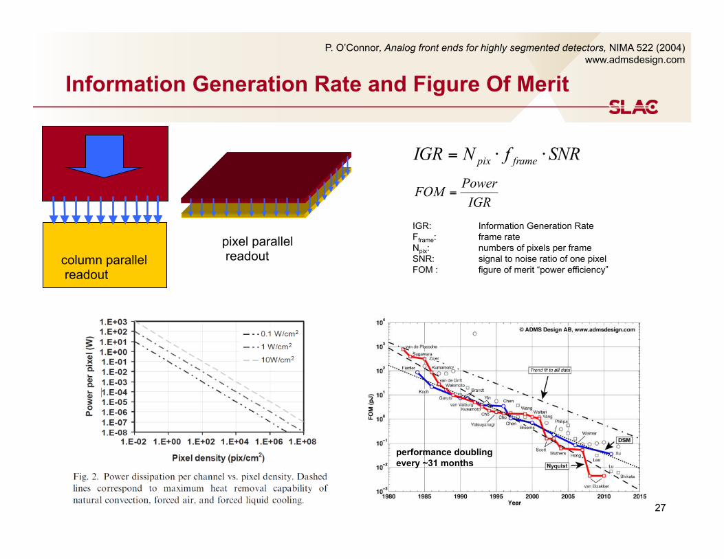
Information Generation Rate and Figure Of Merit
SNRfNIGR framepix ⋅⋅=
column parallel readout
pixel parallel readout
IGRPowerFOM =
IGR: Information Generation Rate Fframe: frame rate Npix: numbers of pixels per frame SNR: signal to noise ratio of one pixel FOM : figure of merit “power efficiency”
performance doubling every ~31 months
P. O’Connor, Analog front ends for highly segmented detectors, NIMA 522 (2004) www.admsdesign.com
27
take home bullets from the (short) electronics part
• low detector capacitance is important for noise performance • low noise performance needs lots of power • high speed per channel kills the noise performance
• high dynamic range, many pixels and high framerates push on the Information Generation Rate (IGR)
• for a given technology there is a practical limit on the IGR in a given area ! • high IGR densities are more prone to crosstalk problems • if one demands to much one has to do R&D to push the FOM in our field • there might be some room to push on thermo-mechanical packaging to harvest improvements
next : hybrid pixel detectors
28
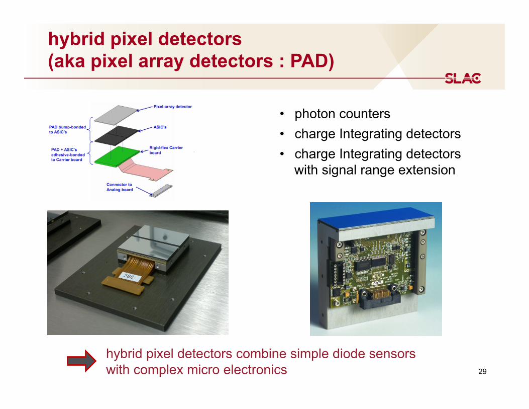
hybrid pixel detectors (aka pixel array detectors : PAD)
• photon counters • charge Integrating detectors • charge Integrating detectors
with signal range extension
hybrid pixel detectors combine simple diode sensors with complex micro electronics 29
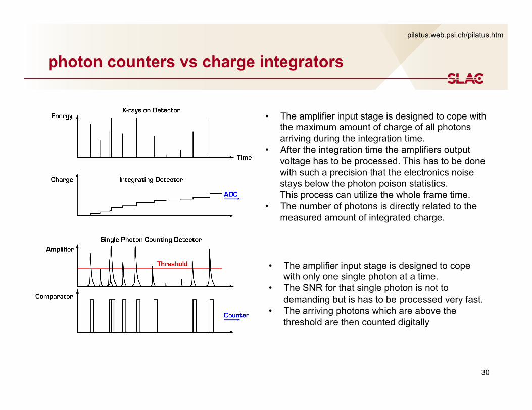
photon counters vs charge integrators
• The amplifier input stage is designed to cope with only one single photon at a time.
• The SNR for that single photon is not to demanding but is has to be processed very fast.
• The arriving photons which are above the threshold are then counted digitally
• The amplifier input stage is designed to cope with the maximum amount of charge of all photons arriving during the integration time.
• After the integration time the amplifiers output voltage has to be processed. This has to be done with such a precision that the electronics noise stays below the photon poison statistics. This process can utilize the whole frame time.
• The number of photons is directly related to the measured amount of integrated charge.
pilatus.web.psi.ch/pilatus.htm
30
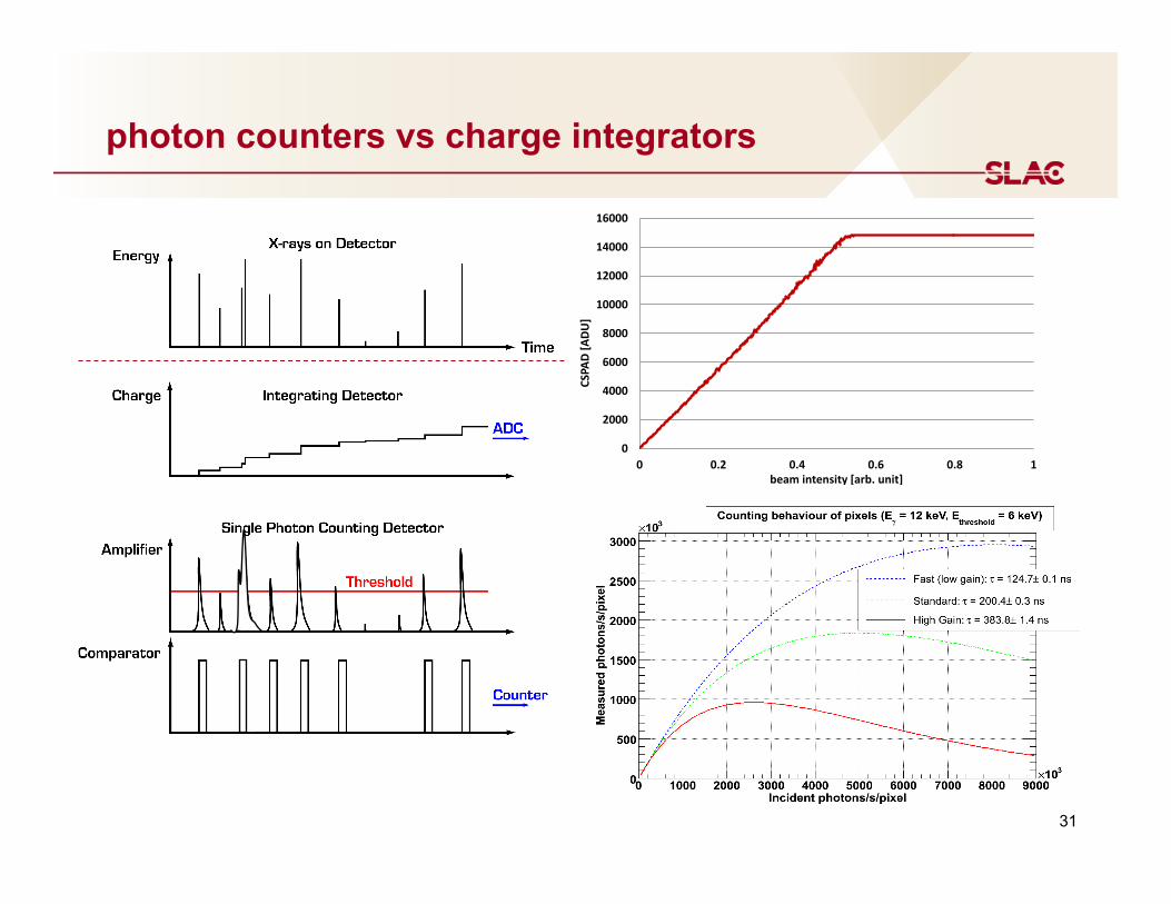
photon counters vs charge integrators
0
2000
4000
6000
8000
10000
12000
14000
16000
0 0.2 0.4 0.6 0.8 1
CSPA
D [ADU
]
beam intensity [arb. unit]
31
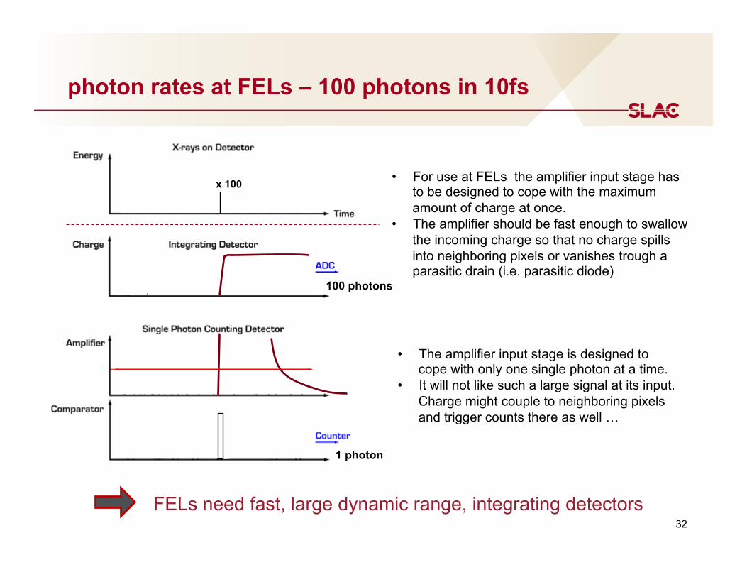
photon rates at FELs – 100 photons in 10fs
x 100
100 photons
1 photon
• The amplifier input stage is designed to cope with only one single photon at a time.
• It will not like such a large signal at its input. Charge might couple to neighboring pixels and trigger counts there as well …
• For use at FELs the amplifier input stage has to be designed to cope with the maximum amount of charge at once.
• The amplifier should be fast enough to swallow the incoming charge so that no charge spills into neighboring pixels or vanishes trough a parasitic drain (i.e. parasitic diode)
FELs need fast, large dynamic range, integrating detectors 32
S&H
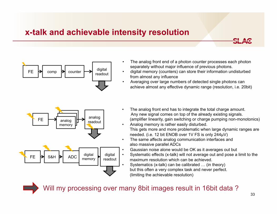
x-talk and achievable intensity resolution
• The analog front end of a photon counter processes each photon separately without major influence of previous photons.
• digital memory (counters) can store their information undisturbed from almost any influence
• Averaging over large numbers of detected single photons can achieve almost any effective dynamic range (resolution, i.e. 20bit)
• The analog front end has to integrate the total charge amount. Any new signal comes on top of the already existing signals. (amplifier linearity, gain switching or charge pumping non-monotonics)
• Analog memory is rather easily disturbed. This gets more and more problematic when large dynamic ranges are needed. (i.e. 12 bit ENOB over 1V FS is only 244µV)
• The same affects analog communication interfaces and also massive parallel ADCs
• Gaussian noise alone would be OK as it averages out but • Systematic effects (x-talk) will not average out and pose a limit to the
maximum resolution which can be achieved. • Systematics (x-talk) can be calibrated … (in theory)
but this often a very complex task and never perfect. (limiting the achievable resolution)
FE comp counter digital readout
FE S&H analog readout analog
memory
FE S&H ADC digital readout
digital memory
Will my processing over many 8bit images result in 16bit data ? 33
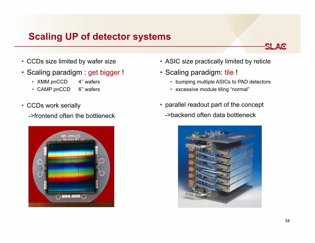
Scaling UP of detector systems
• ASIC size practically limited by reticle
• Scaling paradigm: tile ! • bumping multiple ASICs to PAD detectors • excessive module tiling “normal”
• parallel readout part of the concept ->backend often data bottleneck
• CCDs size limited by wafer size
• Scaling paradigm : get bigger ! • XMM pnCCD 4’’ wafers • CAMP pnCCD 6’’ wafers
• CCDs work serially ->frontend often the bottleneck
34
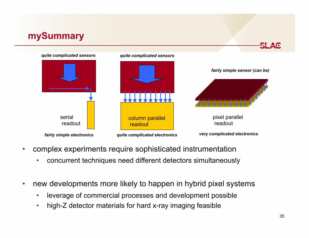
mySummary
• complex experiments require sophisticated instrumentation • concurrent techniques need different detectors simultaneously
• new developments more likely to happen in hybrid pixel systems • leverage of commercial processes and development possible • high-Z detector materials for hard x-ray imaging feasible
serial readout
column parallel readout
pixel parallel readout
quite complicated sensors
quite complicated electronics
quite complicated sensors
fairly simple electronics
fairly simple sensor (can be)
very complicated electronics
35