Embed Size (px)
Citation preview
Hot-embossing replication of self-centering optical fiber alignmentstructures prototyped by deep protonwriting
Evert EbraertMarkus WissmannMarkus GuttmannAlexander KolewMatthias WorgullNicole BariéMarc SchneiderAndreas HofmannStefano BeriJan WattéHugo ThienpontJürgen Van Erps
Evert Ebraert, Markus Wissmann, Markus Guttmann, Alexander Kolew, Matthias Worgull, Nicole Barié,Marc Schneider, Andreas Hofmann, Stefano Beri, Jan Watté, Hugo Thienpont, Jürgen Van Erps, “Hot-embossing replication of self-centering optical fiber alignment structures prototyped by deep protonwriting,” Opt. Eng. 55(7), 076112 (2016), doi: 10.1117/1.OE.55.7.076112.
Hot-embossing replication of self-centering optical fiberalignment structures prototyped by deep proton writing
Evert Ebraert,a,* Markus Wissmann,b Markus Guttmann,b Alexander Kolew,b Matthias Worgull,b Nicole Barié,b
Marc Schneider,b Andreas Hofmann,b Stefano Beri,c Jan Watté,c Hugo Thienpont,a and Jürgen Van Erpsa
aVrije Universiteit Brussel, Department of Applied Physics and Photonics, Brussels Photonics Team (B-PHOT), Pleinlaan 2,B-1050 Brussels, BelgiumbKarlsruhe Institute of Technology (KIT), Institute for Microstructure Technology (IMT), Hermann-von-Helmholtz-Platz 1, 76344Eggenstein-Leopoldshafen, GermanycCommscope, R&D Optics Advanced Engineering, Diestsesteenweg 692, 3010 Kessel-Lo, Belgium
Abstract. This paper presents the hot-embossing replication of self-centering fiber alignment structures for high-precision, single-mode optical fiber connectors. To this end, a metal mold insert was fabricated by electroforminga polymer prototype patterned by means of deep proton writing (DPW). To achieve through-hole structures, wedeveloped a postembossing process step to remove the residual layer inherently present in hot-embossed struc-tures. The geometrical characteristics of the hot-embossed replicas are compared, before and after removal ofthe residual layer, with the DPW prototypes. Initial measurements on the optical performance of the replicas areperformed. The successful replication of these components paves the way toward low-cost mass replication ofDPW-fabricated prototypes in a variety of high-tech plastics. © 2016 Society of Photo-Optical Instrumentation Engineers (SPIE)[DOI: 10.1117/1.OE.55.7.076112]
Keywords: alignment structures; deep proton writing; electroforming; fiber connector; hot embossing; micromilling; mold insert; poly-mer replication; precision alignment.
Paper 160808P received May 24, 2016; accepted for publication Jul. 7, 2016; published online Jul. 22, 2016.
1 IntroductionThe relentlessly increasing demand for bandwidth, mainlydriven by cloud-based services and (ultra-)high-definitionvideo-on-demand services, pushes the need for high-bitrateInternet connections. The only future-proof solution for suchhigh-speed networks is to use optical fiber and bring it asclose as possible to the end user—ultimately, into the sub-scriber’s home.1–3 To deploy “fiber to the home” on a mas-sive scale, there is a strong need for robust and easy-to-use,but at the same time high-performance, fiber connectivitysolutions. These solutions must allow for physical mating ofsingle-mode fibers with very low loss, or in other words,with submicrometer alignment accuracy. To this end, wehave designed a self-centering alignment system (SCAS),which centers a fiber upon insertion to ensure a good lateralalignment accuracy between two mated single-modefibers.4,5 This SCAS is based on deflectable microspringsthat exert a force on the fiber while it is being inserted.6,7
The advantage of self-centering fiber connectors is thatthey can mitigate the effect of the fabrication tolerance (oftypically �0.7 μm and up to �1.0 μm8) on the claddingdiameter of G.652 standard telecom single-mode fiber, asopposed to more traditional connector approaches makinguse of ferrules or V-grooves.9 We have recently shown thatan insertion loss down to 0.1 dB can be achieved with con-nector assemblies based on prototype SCAS componentsfabricated through deep proton writing (DPW).5 Given thevery high number of fiber connections that need to beinstalled when rolling out a fiber-to-the-home network, itis imperative that those components can be made at low
cost and in high volumes. In addition, the componentsshould be compatible with stringent environmental condi-tions, such as an operating temperature ranging from−40°C to 70°C.10 This means that the parts should be fab-ricated of high-performance plastics with replication tech-nologies such as microinjection molding or hot embossing.11
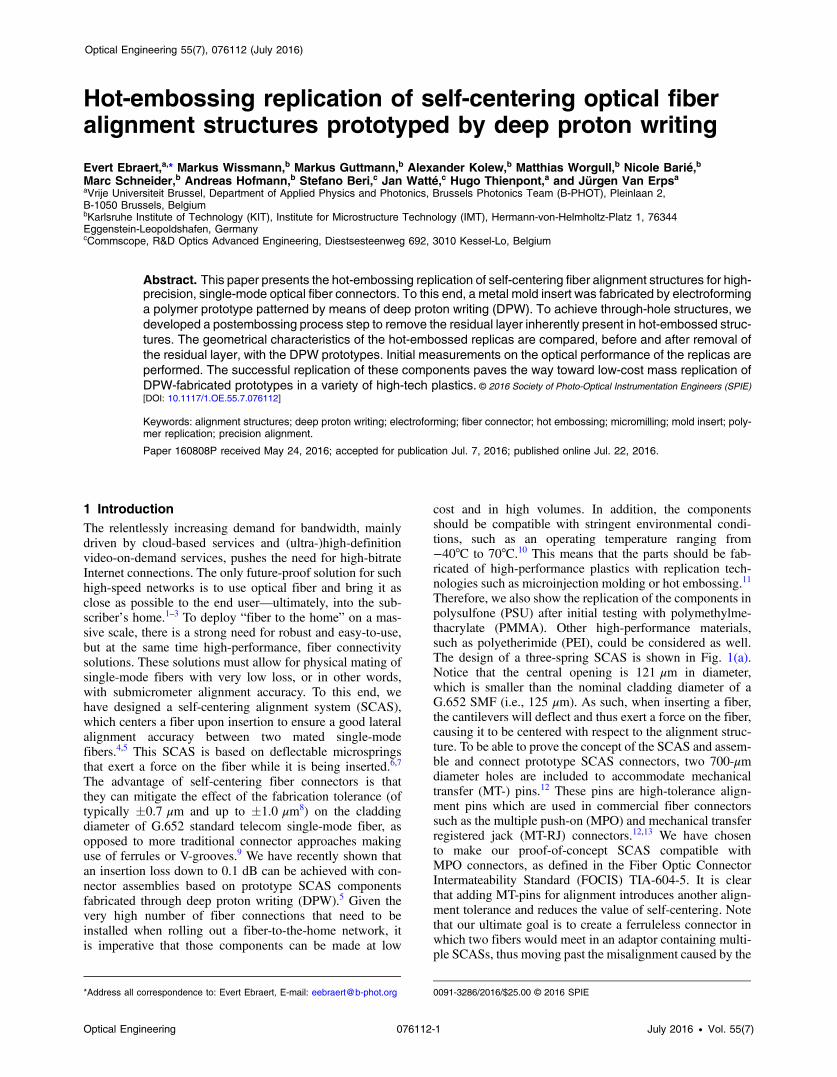
Therefore, we also show the replication of the components inpolysulfone (PSU) after initial testing with polymethylme-thacrylate (PMMA). Other high-performance materials,such as polyetherimide (PEI), could be considered as well.The design of a three-spring SCAS is shown in Fig. 1(a).Notice that the central opening is 121 μm in diameter,which is smaller than the nominal cladding diameter of aG.652 SMF (i.e., 125 μm). As such, when inserting a fiber,the cantilevers will deflect and thus exert a force on the fiber,causing it to be centered with respect to the alignment struc-ture. To be able to prove the concept of the SCAS and assem-ble and connect prototype SCAS connectors, two 700-μmdiameter holes are included to accommodate mechanicaltransfer (MT-) pins.12 These pins are high-tolerance align-ment pins which are used in commercial fiber connectorssuch as the multiple push-on (MPO) and mechanical transferregistered jack (MT-RJ) connectors.12,13 We have chosento make our proof-of-concept SCAS compatible withMPO connectors, as defined in the Fiber Optic ConnectorIntermateability Standard (FOCIS) TIA-604-5. It is clearthat adding MT-pins for alignment introduces another align-ment tolerance and reduces the value of self-centering. Notethat our ultimate goal is to create a ferruleless connector inwhich two fibers would meet in an adaptor containing multi-ple SCASs, thus moving past the misalignment caused by the
*Address all correspondence to: Evert Ebraert, E-mail: [email protected] 0091-3286/2016/$25.00 © 2016 SPIE
Optical Engineering 076112-1 July 2016 • Vol. 55(7)
Optical Engineering 55(7), 076112 (July 2016)
fabrication tolerances on both the alignment ferrules and thefiber. The aspect ratio of the SCAS is 5∶1 (500-μm deep and100-μm wide cavities). In this paper, we discuss the use ofhot embossing for the replication of SCAS components. InSec. 2, we describe the DPW technology that was used forprototyping the master component in PMMA. We also dis-cuss the justified partial metallization of that master compo-nent in order to realize a metal mold insert throughelectroforming. Finally, we discuss the hot-embossing repli-cation of these structures in PMMA14 and PSU and theadapted micromilling process we developed to remove theresidual layer inherently present in the hot-embossed repli-cas. In Sec. 3, we describe the results of the hot embossingand residual layer removal and characterize the geometricaldimensions of the replicas with the master component fab-ricated through DPW. Last but not least, we perform opticalinsertion loss measurements of fiber connector assembliesmaking use of the fabricated replicas.
2 Technology Description and ExperimentalMethods
2.1 Prototyping by Deep Proton Writing
DPW is a rapid prototyping technology for micro-opticaland micromechanical components.15 DPW finds its originsin the LIGA technology (Lithographie, Galvanoformung,Abformung)16 but uses protons rather than x-rays for the irra-diation process. In addition, DPW is a direct writing processin which the desired proton-beam diameter is selected in astopping mask, and the sample is moved perpendicularly tothe proton beam according to a predefined pattern (i.e., thedesign of the SCAS in this case). The stopping mask consistsof two stacked 350-μm thick nickel plates with aperturesranging from 50 to 300 μm. This allows us to work with pro-ton energies of up to 16.5 MeV,17 which enables irradiationof PMMA samples that are up to 2-mm thick.18 The conceptof DPW is based on the fact that irradiating high-molecular-weight PMMA (Mw ≈ 106 g∕mol) with high-energy protonswill break the long polymer chains. This will cause thephysical and chemical material properties in the irradiatedzones to be very different from those in the unexposedbulk material. This will, in turn, allow the irradiated zones
to be selectively etched away in so-called GG developer(which consists of 60% diethylene glycol monobutylether, 20% morpholine, 5% 2-aminoethanol, and 15%de-ionized water) during 105 min at 38°C while using anultrasonic stirrer.15 This way, DPW enables high-qualityprototyping of (arrays of) microholes,19 micropillars,17 andmicromirrors with optical quality sidewalls.15 An importantcharacteristic of DPW is that the protons scatter within thesample material during irradiation, causing a slightly conicalshape when irradiating microholes.19 In this case, the conicalshape is an asset, since it both facilitates the fiber insertion inthe SCAS (by avoiding perfectly vertical and flat sidewalls)and the demolding of replicas. The DPW-prototyped masterof a three-spring SCAS structure is shown in Fig. 1(b). Sincethe SCAS is designed with a thickness of 500 μm, a protonenergy of 12 MeV was used, as this is sufficient to guaranteefull traversal of the protons through the sample, and higherenergies would cause a higher amount of surface damage dueto stray protons and the long irradiation times required forthe SCAS. Since the smallest cavity in the SCAS is 100-μmwide, the resulting aspect ratio is 5∶1. This component wasirradiated using the smallest available proton beam, with adiameter of 50 μm, to be able to pattern the fine features ofthe central hole region in the SCAS. The proton fluence wasoptimized to 5.2 × 10⁸ protons∕μm2 to achieve the desireddimensional shape. The total irradiation time for two 700-μmdiameter alignment holes and the SCAS is about 5 h. Hence,it is clear that DPW is a costly and time-consuming process,ideally suited for rapid prototyping but not for large-volumeproduction. Note that self-centering optical fiber holders,created by combining proton beam writing and symmetricswelling of PMMA, have previously been reported.20 Thisapproach requires the diffusion of a monomer into a DPW-irradiated PMMA sample while a fiber is inserted into theirradiated and partly etched microholes. It is clear that thistechnique is not at all scalable to large-scale production.
2.2 Mold Insert Formation
Although DPW is not a mass replication technique as such,one of the assets of DPW is that once the master componenthas been prototyped, a metal mold can be generated from themaster by applying a combination of joining technology and
6.4 mm
2.5m
m
4.6 mm
MT-pinhole
Central opening
MT-pinhole
(a) (b)
Fig. 1 (a) Design of a three-spring SCAS, designed to be compatible with commercial MPO connectors.(b) Prototype SCAS fabricated in PMMA with DPW.
Optical Engineering 076112-2 July 2016 • Vol. 55(7)
Ebraert et al.: Hot-embossing replication of self-centering optical fiber alignment structures. . .
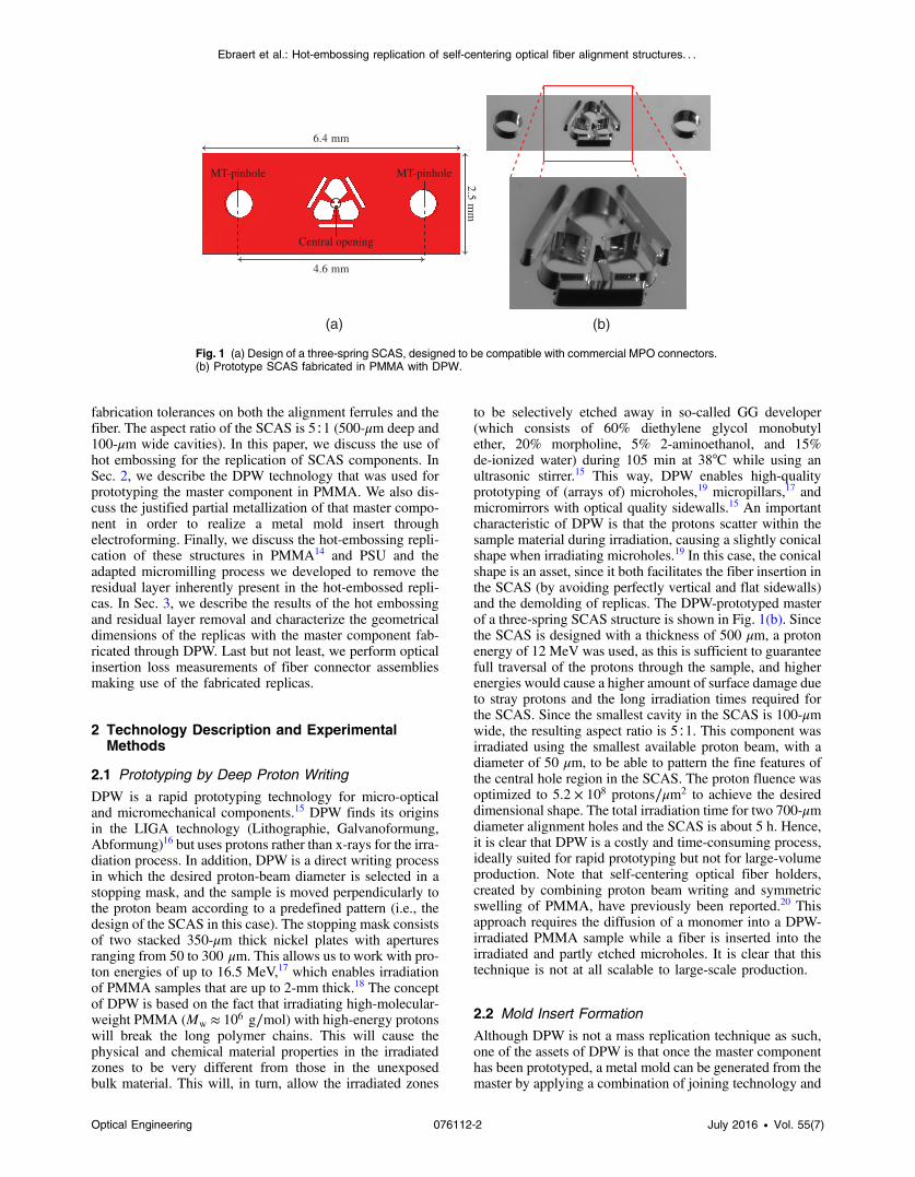
electroforming. Electroforming of PMMA master compo-nents has been known for a long time,21 and we have pre-viously shown the successful application of this method forthe replication of DPW-prototyped micromirror structures.22
However, as opposed to the latter components, the currentself-centering fiber alignment structures contain through-holes and small cavities, which could induce errors likeincomplete filling or underplating during the electroformingprocess. To avoid those errors, we have developed a justifiedpartial metallization process for the mold formation.23 Thisprocess requires the DPW prototype to be attached to a cop-per substrate. To avoid excessive amounts of adhesive in thesmall through-holes, a dip method was used to apply adhe-sive to the prototype structure. Even with this special dipmethod, some adhesive covered the copper substrate in thesmallest features, leading to an undesired “rounding” effectas illustrated in the scanning electron microscope (SEM)image of the mold insert in Fig. 2(a). To minimize this effect,laser ablation was used to remove the adhesive in thesethrough-holes and reveal the copper substrate for subsequentelectroforming. To ensure that the electroforming starts byfilling the small through-holes and covers the rest of thestructure only after filling those through-holes, a seed layeris deposited on the structure with physical vapor depositionthrough a mask.23 This allows us to avoid defects like voidspaces or loose parts in the electroformed nickel mold. Thefinal step of the mold insert fabrication consists of cutting themold insert to its desired dimensions by wire electron dis-charge machine cutting.
2.3 Replication by Hot Embossing
The mold insert is inserted in the upper part of ourhot-embossing equipment (a HEX03 from JenoptikMikrotechnik GmbH). The lower part of the hot embosserconsists of a demolding plate with a high surface roughness(sandblasted stainless steel) to facilitate the demolding ofreplicas. Both the upper and lower parts can be heated upto 280°C and can maintain a pressure of up to 200 kN.The materials considered for the self-centering alignmentstructure replicas are PSU and PMMA. PMMA is selectedbecause of our previous experience with this material forhot embossing as well as to enable a comparison betweenthe DPW prototype and its replicas in the same material.
PSU is a polymer, which is commonly used for microhotembossing,24,25 shows a high resistance to creep and is com-patible with the stringent environmental conditions discussedin Sec. 1.26 The embossing process begins with placing a20 × 20 × 2 mm3 piece of PMMA or PSU on the demoldingplate. Then the upper and lower parts of the embosser closeand form a vacuum chamber which is evacuated to a pressurebelow 100 mbar. The mold insert and demolding plate aresubsequently heated up to 180°C or 235°C for the replicationin, respectively, PMMA or PSU. Once this temperature isreached the actual embossing happens with a force of50 kN, which is maintained for 5 min. Then the system iscooled down to 80°C while holding the force at 50 kN inorder to minimize the effect of shrinkage of the polymer andto prevent void spaces from forming in the embossed struc-ture. After cooling down, the upper and lower parts arepulled apart, and the replica sticks to the demolding platebecause the friction of the replica with the sand-blasteddemolding plate is larger than the friction with the moldinsert. The total cycle time for an SCAS component to bereplicated is about 30 min. An SEM image of a silver-platedPMMA replica can be seen in Fig. 2(b).
2.4 Residual Layer Removal
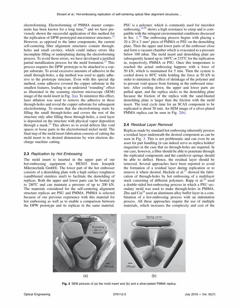
Replicas made by standard hot embossing inherently possessa residual layer underneath the desired component as can beseen in Fig. 3. This is not problematic and can even be anasset for part handling (it can indeed serve as replica holder/magazine) in the case that no through-holes are required. Inour case, however, a fiber should be able to penetrate throughthe replicated components and the cantilever springs shouldbe able to deflect. Hence, the residual layer should beremoved. Several approaches have been reported to avoidthe formation of a residual layer during replication or toremove it where desired. Heckele et al.27 showed the fabri-cation of through-holes by hot embossing of a multilayerstack consisting of different polymers. Rapp et al.28 useda double-sided hot-embossing process in which a PSU sec-ondary mold was used to make through-holes in PMMA.Zhu and Cui29 used an aluminum alloy buffer layer in a com-bination of a hot-embossing process with an indentationprocess. All these approaches require the use of multiplematerials, which increases the complexity and cost of the
Roundingdue to
adhesive
100 m
Spring cavity
100 m
(a) (b)
µ µ
Fig. 2 SEM pictures of (a) the mold insert and (b) and a silver-plated PMMA replica.
Optical Engineering 076112-3 July 2016 • Vol. 55(7)
Ebraert et al.: Hot-embossing replication of self-centering optical fiber alignment structures. . .
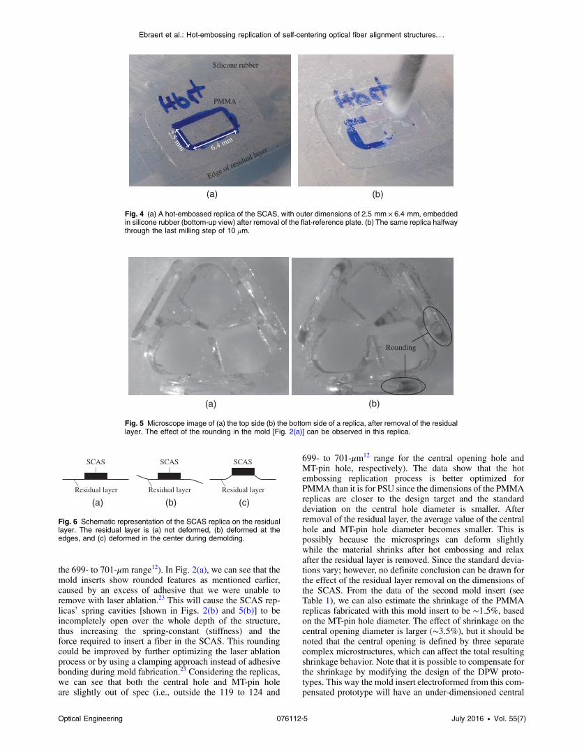
hot-embossing process. We present an alternative approachto remove the residual layer through a post-embossingprocessing step consisting of a combination of siliconemolding30 and conventional micromilling. For visual identi-fication, we first mark the residual layer directly around thereplica and then cut the residual layer down to a small size (of∼15 mm × ∼20 mm) in order to increase the amount of rep-licas we can process simultaneously. It is also possible thatmultiple SCAS structures are included in a single moldinsert, which would allow for multiple replicas to be moldedat the same time, sharing the same residual layer. Replicasare then placed bottom-down on a flat reference plate andsubsequently embedded into a liquid silicone, which is amixture of a rubber (10 parts by weight) and a catalyst (1part by weight). The silicone rubber (Rhodorsil RTV 246A)contains approximately 90% (by weight) methyl-vinyl-poly-siloxane, <1% hexamethydisilazane, 9% amorphous silica,and <0.5% modified chloroplatinic acid. The silicone cata-lyst (MCP-HEK CAT750) is a hydride-terminated poly-dimethyl-siloxane. When cutting down the size of theresidual layer around each replica, care needs to be takento maintain enough residual layer surface. This allows theliquid silicone rubber to apply sufficient pressure to pushthe replica down against the flat reference plate. If not,the replica could be embedded in the silicone under anangle, which could severely impede the subsequent residuallayer removal process. In cases where multiple replicas areincluded on a single residual layer, this is not an issue. TheCAT750 catalyst ensures hardening of the silicone over aperiod of 24 h after mixing with the silicone rubber. Somesilicone flows under the edges of the residual layer. Whenremoving the flat reference plate, the residual layer’s bottomside is thus partially submerged in silicone rubber and par-tially free, as can be seen in Fig. 4(a) for a hot-embossedreplica of an SCAS with outer dimensions of 2.5 mm ×6.4 mm. After hardening, the silicone rubber mold can bemounted on a conventional micromilling machine (a VHFCAM 100 in our case), which we have equipped with aVolpi AS 11∕50 video microprobe and CCD-camera for vis-ual alignment of the structure with respect to the milling tool.The residual layer is milled away with a step-wise approach.A double-tooth cutter with fishtail of 3-mm diameter is usedat 8000 rpm with a cutting speed of 0.3 mm∕s. Starting witha manual touch-down of the milling tool, 10 μm is milledaway from the residual layer each step, until the residuallayer of the SCAS is fully removed. The reason we chooseto take steps of 10 μm is that this is our micromilling
machine’s resolution. As can be seen in Fig. 4(b), the replicais free of residual layer once the marked zone around theSCAS is milled away. A microscope image of the surfaceafter micromilling can be seen in Fig. 5(b). After optimiza-tion of this method, we were able to successfully remove theresidual layer of the SCAS replicas with a yield higher than80% for both the PMMA and PSU replicas. The main reasonfor failures is the deformation of the residual layer of certainreplicas during demolding. This deformation can manifestitself as a bending of the edge of the residual layer asdepicted in Fig. 6(a). This can lead to the sample beingmounted under an angle in the micromilling machine asmentioned earlier. The deformation can also manifest itselfin the center of the residual layer, where the SCAS is located,as depicted in Fig. 6(b). In this case, the visual feedbackmethod [i.e., the marked zone being milled away, asshown in Fig. 4(b)], will not be adequate to accurately deter-mine when the residual layer is removed. This gives rise tothe operator of the micromilling machine to either removetoo little of the residual layer or to continue milling afterthe SCAS has been removed. Either one of the above-described cases or a combination can lead to damaged micro-springs in the SCAS and thus unusable components.
3 Results
3.1 Geometrical Characterization
The mold inserts fabricated by electroforming DPW proto-types (described in Sec. 2.2) and the replicas made fromthese mold inserts by hot embossing (described inSec. 2.3) are measured using a Werth UA-400 multisensorcoordinate measure machine (CMM). For the geometricalcharacterization, we focus on measuring two critical featuresof the SCAS: the diameter of the central opening and of theMT-pin holes as indicated in Fig. 1(a). When the centralopening becomes larger than 126 μm in diameter, the struc-ture will no longer exhibit any self-centering functionalitysince the cladding diameter of a G.652 SMF is 125� 1 μmas mentioned earlier. The smaller the central hole becomes,the more force will be required to insert a fiber. Therefore, itis important that the central hole diameter is in the range of121 to 124 μm to avoid nonfunctional SCAS structures. Inan MPO-compatible connector assembly, the MT-pin holesare used to align two connector assemblies in order to makea physical fiber connection (mechanical splice). Hence, theMT-pin hole size and position are also crucial to the func-tionality of the SCAS. In our case, two SCAS connectorassemblies can be connected or one SCAS connectorassembly can be connected to an MPO connector. To opti-mize the electroforming process, six DPW prototypes wereselected, based on their dimensions, to use for creating moldinserts. The results of the final two electroformed moldinserts are shown in Table 1. Since one mold insert was dam-aged during the optimization of the hot-embossing processfor the replication of components in PSU, there is no geo-metrical data available on that insert. (The electroformedmold insert was not measured prior to replication testsbecause the CMM measurements took place at a differentlocation than the electroforming and hot embossing.)Regarding the central hole, the second mold insert is inspec (i.e., inside the 121- to 124-μm range12). For theMT-pin hole though, it is slightly out of spec (i.e., outside
SCAS replica
Residual layer
Fig. 3 A hot-embossed SCAS replica in PMMA with residual layer cutdown to size (∼15 mm × ∼20 mm) for residual layer removal.
Optical Engineering 076112-4 July 2016 • Vol. 55(7)
Ebraert et al.: Hot-embossing replication of self-centering optical fiber alignment structures. . .
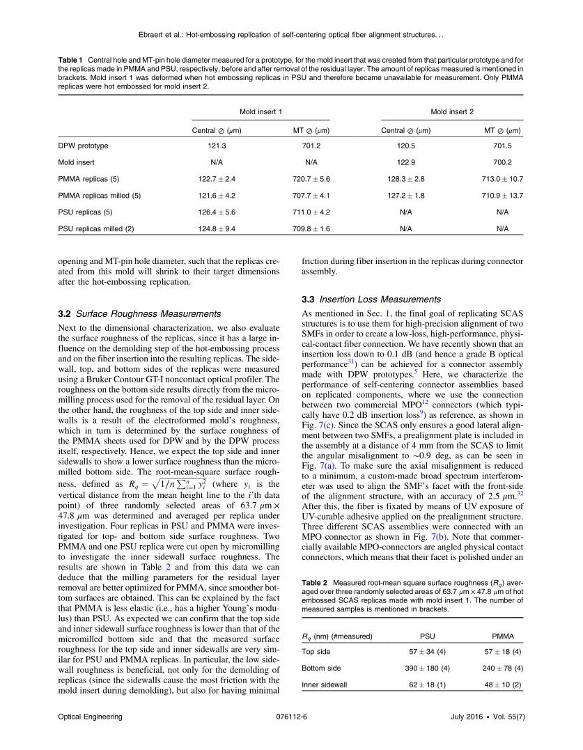
the 699- to 701-μm range12). In Fig. 2(a), we can see that themold inserts show rounded features as mentioned earlier,caused by an excess of adhesive that we were unable toremove with laser ablation.23 This will cause the SCAS rep-licas’ spring cavities [shown in Figs. 2(b) and 5(b)] to beincompletely open over the whole depth of the structure,thus increasing the spring-constant (stiffness) and theforce required to insert a fiber in the SCAS. This roundingcould be improved by further optimizing the laser ablationprocess or by using a clamping approach instead of adhesivebonding during mold fabrication.23 Considering the replicas,we can see that both the central hole and MT-pin holeare slightly out of spec (i.e., outside the 119 to 124 and
699- to 701-μm12 range for the central opening hole andMT-pin hole, respectively). The data show that the hotembossing replication process is better optimized forPMMA than it is for PSU since the dimensions of the PMMAreplicas are closer to the design target and the standarddeviation on the central hole diameter is smaller. Afterremoval of the residual layer, the average value of the centralhole and MT-pin hole diameter becomes smaller. This ispossibly because the microsprings can deform slightlywhile the material shrinks after hot embossing and relaxafter the residual layer is removed. Since the standard devia-tions vary; however, no definite conclusion can be drawn forthe effect of the residual layer removal on the dimensions ofthe SCAS. From the data of the second mold insert (seeTable 1), we can also estimate the shrinkage of the PMMAreplicas fabricated with this mold insert to be ∼1.5%, basedon the MT-pin hole diameter. The effect of shrinkage on thecentral opening diameter is larger (∼3.5%), but it should benoted that the central opening is defined by three separatecomplex microstructures, which can affect the total resultingshrinkage behavior. Note that it is possible to compensate forthe shrinkage by modifying the design of the DPW proto-types. This way the mold insert electroformed from this com-pensated prototype will have an under-dimensioned central
Rounding
(a) (b)
Fig. 5 Microscope image of (a) the top side (b) the bottom side of a replica, after removal of the residuallayer. The effect of the rounding in the mold [Fig. 2(a)] can be observed in this replica.
SCAS
Residual layer
SCAS
Residual layer
SCAS
Residual layer
(a) (b) (c)
Fig. 6 Schematic representation of the SCAS replica on the residuallayer. The residual layer is (a) not deformed, (b) deformed at theedges, and (c) deformed in the center during demolding.
PMMA
Edgeof re
sidual la
yer
Silicone rubber
6.4mm
2.5mm
(a) (b)
Fig. 4 (a) A hot-embossed replica of the SCAS, with outer dimensions of 2.5 mm × 6.4 mm, embeddedin silicone rubber (bottom-up view) after removal of the flat-reference plate. (b) The same replica halfwaythrough the last milling step of 10 μm.
Optical Engineering 076112-5 July 2016 • Vol. 55(7)
Ebraert et al.: Hot-embossing replication of self-centering optical fiber alignment structures. . .
opening and MT-pin hole diameter, such that the replicas cre-ated from this mold will shrink to their target dimensionsafter the hot-embossing replication.
3.2 Surface Roughness Measurements
Next to the dimensional characterization, we also evaluatethe surface roughness of the replicas, since it has a large in-fluence on the demolding step of the hot-embossing processand on the fiber insertion into the resulting replicas. The side-wall, top, and bottom sides of the replicas were measuredusing a Bruker Contour GT-I noncontact optical profiler. Theroughness on the bottom side results directly from the micro-milling process used for the removal of the residual layer. Onthe other hand, the roughness of the top side and inner side-walls is a result of the electroformed mold’s roughness,which in turn is determined by the surface roughness ofthe PMMA sheets used for DPW and by the DPW processitself, respectively. Hence, we expect the top side and innersidewalls to show a lower surface roughness than the micro-milled bottom side. The root-mean-square surface rough-ness, defined as Rq ¼
ffiffiffiffiffiffiffiffiffiffiffiffiffiffiffiffiffiffiffiffiffiffiffiffi1∕n
Pni¼1 y
2i
p(where yi is the
vertical distance from the mean height line to the i’th datapoint) of three randomly selected areas of 63.7 μm ×47.8 μm was determined and averaged per replica underinvestigation. Four replicas in PSU and PMMA were inves-tigated for top- and bottom side surface roughness. TwoPMMA and one PSU replica were cut open by micromillingto investigate the inner sidewall surface roughness. Theresults are shown in Table 2 and from this data we candeduce that the milling parameters for the residual layerremoval are better optimized for PMMA, since smoother bot-tom surfaces are obtained. This can be explained by the factthat PMMA is less elastic (i.e., has a higher Young’s modu-lus) than PSU. As expected we can confirm that the top sideand inner sidewall surface roughness is lower than that of themicromilled bottom side and that the measured surfaceroughness for the top side and inner sidewalls are very sim-ilar for PSU and PMMA replicas. In particular, the low side-wall roughness is beneficial, not only for the demolding ofreplicas (since the sidewalls cause the most friction with themold insert during demolding), but also for having minimal
friction during fiber insertion in the replicas during connectorassembly.
3.3 Insertion Loss Measurements
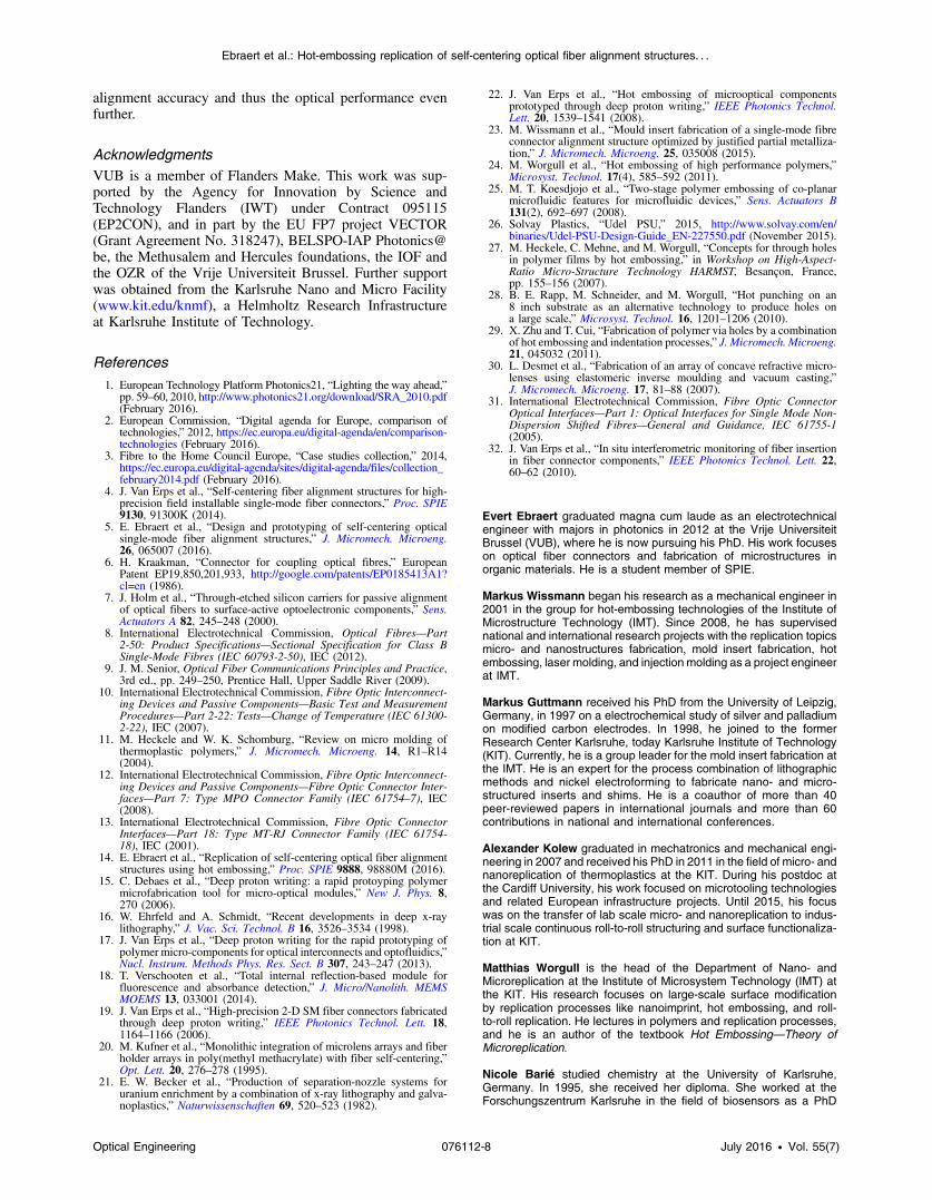
As mentioned in Sec. 1, the final goal of replicating SCASstructures is to use them for high-precision alignment of twoSMFs in order to create a low-loss, high-performance, physi-cal-contact fiber connection. We have recently shown that aninsertion loss down to 0.1 dB (and hence a grade B opticalperformance31) can be achieved for a connector assemblymade with DPW prototypes.5 Here, we characterize theperformance of self-centering connector assemblies basedon replicated components, where we use the connectionbetween two commercial MPO12 connectors (which typi-cally have 0.2 dB insertion loss9) as reference, as shown inFig. 7(c). Since the SCAS only ensures a good lateral align-ment between two SMFs, a prealignment plate is included inthe assembly at a distance of 4 mm from the SCAS to limitthe angular misalignment to ∼0.9 deg, as can be seen inFig. 7(a). To make sure the axial misalignment is reducedto a minimum, a custom-made broad spectrum interferom-eter was used to align the SMF’s facet with the front-sideof the alignment structure, with an accuracy of 2.5 μm.32
After this, the fiber is fixated by means of UV exposure ofUV-curable adhesive applied on the prealignment structure.Three different SCAS assemblies were connected with anMPO connector as shown in Fig. 7(b). Note that commer-cially available MPO-connectors are angled physical contactconnectors, which means that their facet is polished under an
Table 1 Central hole and MT-pin hole diameter measured for a prototype, for the mold insert that was created from that particular prototype and forthe replicas made in PMMA and PSU, respectively, before and after removal of the residual layer. The amount of replicas measured is mentioned inbrackets. Mold insert 1 was deformed when hot embossing replicas in PSU and therefore became unavailable for measurement. Only PMMAreplicas were hot embossed for mold insert 2.
Mold insert 1 Mold insert 2
Central ⊘ (μm) MT ⊘ (μm) Central ⊘ (μm) MT ⊘ (μm)
DPW prototype 121.3 701.2 120.5 701.5
Mold insert N/A N/A 122.9 700.2
PMMA replicas (5) 122.7� 2.4 720.7� 5.6 128.3� 2.8 713.0� 10.7
PMMA replicas milled (5) 121.6� 4.2 707.7� 4.1 127.2� 1.8 710.9� 13.7
PSU replicas (5) 126.4� 5.6 711.0� 4.2 N/A N/A
PSU replicas milled (2) 124.8� 9.4 709.8� 1.6 N/A N/A
Table 2 Measured root-mean square surface roughness (Rq ) aver-aged over three randomly selected areas of 63.7 μm × 47.8 μm of hotembossed SCAS replicas made with mold insert 1. The number ofmeasured samples is mentioned in brackets.
Rq (nm) (#measured) PSU PMMA
Top side 57� 34 (4) 57� 18 (4)
Bottom side 390� 180 (4) 240� 78 (4)
Inner sidewall 62� 18 (1) 48� 10 (2)
Optical Engineering 076112-6 July 2016 • Vol. 55(7)
Ebraert et al.: Hot-embossing replication of self-centering optical fiber alignment structures. . .
8 deg angle. Hence, we had to polish the MPO ferrules per-pendicularly such that a physical connection could be madewith flat-cleaved fibers. The smallest insertion loss was mea-sured to be 0.84 dB when connecting an SCAS connectorassembly from a PMMA replica to a perpendicularly pol-ished MPO connector, as shown in Fig. 7(d). Consideringthe nonideal rounded features in the mold insert [Fig. 2(a)]and in the resulting replicas [Fig. 5(b)] and the fact that wecurrently have not compensated the prototypes for shrinking.These results show that our connector assemblies using thereplicated self-centering alignment structures have the poten-tial to be as performant as current state-of-the-art optical sin-gle-mode fiber connectors, taking into account that we havealready demonstrated insertion losses down to 0.1 dB withthe DPW prototypes.5 To realize this potential, further opti-mization of the prototype (e.g., compensating for the shrink-age), of the mold formation and of the replication process isneeded.
4 ConclusionsWe have shown that a DPW fabricated PMMA prototype ofan SCAS can be used as a template for electroforming anickel mold insert. This mold insert is subsequently usedas a shim for the replication of the SCAS by means ofhot embossing. Successful replication was achieved in twomaterials: PMMA and PSU. Hot embossed replicas inher-ently posses a residual layer underneath the replicated struc-ture which needs to be removed to achieve through-holes inthe SCAS to allow for fiber insertion into the structure. Wedeveloped a method in which we remove the residual layer
by micromilling in steps of 10 μm after encasing the SCASreplica in a silicone rubber with the aim of holding the smallSCAS components in place during the micromilling process.With this method, a yield better than 80% was achieved forresidual layer removal. The SCAS replicas were geometri-cally characterized and were shown to be slightly out ofspec, mainly due to shrinkage. The root-mean square surfaceroughness (Rq) was measured for the inner sidewalls, top andbottom sides of the replicas. As expected, the bottom side(i.e., the micromilled side) showed the highest surfaceroughness (Rq ¼ 240 to 390 nm) while lower values weremeasured for the inner sidewalls and top side (Rq ¼ 48 to62 nm), which facilitates the demolding process as wellas the fiber insertion in the resulting replicas. Finally, theSCAS replicas were used to create MPO-compatible sin-gle-mode fiber connector assemblies and an insertion lossof 0.84 dB was achieved compared to an MPO–MPO refer-ence connection. The rounded features in the mold insert andthe fact that we did not compensate for shrinkage, leads tothe replicas being slightly out of spec. For this reason, envi-ronmental testing of the replicas has not been performed yet.However, taking into account the insertion loss of 0.1 dBobtained with SCAS prototypes,5 this result shows thatthe replicated SCAS has the potential to perform as wellas state-of-the-art connectors after further optimization ofthe prototype (e.g., compensation for shrinkage), of themold formation and of the replication process. Indeed,while, in this paper, we used an MPO-compatible layoutto be able to perform a proof-of-concept demonstration,our ultimate goal is to move toward ferruleless connectorsto fully exploit the potential of the SCAS, improving the
Prealignment plate
Spacer
Self-centering alignment plate
MT-pin
MT-pin
Reference
MPOSource MPO Detector
MT-pin
Insertion loss measurement
SCASSource MPO Detector
MT-pin
(a) (b)
(c) (d)
Fig. 7 SCAS assembly with the prealignment plate in green, spacer in gray, SCAS in red, MT-pins inyellow, and the single-mode fiber in black. (a) This assembly (male) can be aligned with anotherassembly (female) by inserting the MT-pins in the other assembly and pressing them together suchthat physical contact is made. (b) A connection between an SCAS assembly and a perpendicularlypolished MPO ferrule. Schematic representation of (c) the reference measurement between 2 MPOconnectors and (d) the insertion loss measurement between an MPO connector and an SCAS connectorassembly.
Optical Engineering 076112-7 July 2016 • Vol. 55(7)
Ebraert et al.: Hot-embossing replication of self-centering optical fiber alignment structures. . .
alignment accuracy and thus the optical performance evenfurther.
AcknowledgmentsVUB is a member of Flanders Make. This work was sup-ported by the Agency for Innovation by Science andTechnology Flanders (IWT) under Contract 095115(EP2CON), and in part by the EU FP7 project VECTOR(Grant Agreement No. 318247), BELSPO-IAP Photonics@be, the Methusalem and Hercules foundations, the IOF andthe OZR of the Vrije Universiteit Brussel. Further supportwas obtained from the Karlsruhe Nano and Micro Facility(www.kit.edu/knmf), a Helmholtz Research Infrastructureat Karlsruhe Institute of Technology.
References
1. European Technology Platform Photonics21, “Lighting the way ahead,”pp. 59–60, 2010, http://www.photonics21.org/download/SRA_2010.pdf(February 2016).
2. European Commission, “Digital agenda for Europe, comparison oftechnologies,” 2012, https://ec.europa.eu/digital-agenda/en/comparison-technologies (February 2016).
3. Fibre to the Home Council Europe, “Case studies collection,” 2014,https://ec.europa.eu/digital-agenda/sites/digital-agenda/files/collection_february2014.pdf (February 2016).
4. J. Van Erps et al., “Self-centering fiber alignment structures for high-precision field installable single-mode fiber connectors,” Proc. SPIE9130, 91300K (2014).
5. E. Ebraert et al., “Design and prototyping of self-centering opticalsingle-mode fiber alignment structures,” J. Micromech. Microeng.26, 065007 (2016).
6. H. Kraakman, “Connector for coupling optical fibres,” EuropeanPatent EP19,850,201,933, http://google.com/patents/EP0185413A1?cl=en (1986).
7. J. Holm et al., “Through-etched silicon carriers for passive alignmentof optical fibers to surface-active optoelectronic components,” Sens.Actuators A 82, 245–248 (2000).
8. International Electrotechnical Commission, Optical Fibres—Part2-50: Product Specifications—Sectional Specification for Class BSingle-Mode Fibres (IEC 60793-2-50), IEC (2012).
9. J. M. Senior, Optical Fiber Communications Principles and Practice,3rd ed., pp. 249–250, Prentice Hall, Upper Saddle River (2009).
10. International Electrotechnical Commission, Fibre Optic Interconnect-ing Devices and Passive Components—Basic Test and MeasurementProcedures—Part 2-22: Tests—Change of Temperature (IEC 61300-2-22), IEC (2007).
11. M. Heckele and W. K. Schomburg, “Review on micro molding ofthermoplastic polymers,” J. Micromech. Microeng. 14, R1–R14(2004).
12. International Electrotechnical Commission, Fibre Optic Interconnect-ing Devices and Passive Components—Fibre Optic Connector Inter-faces—Part 7: Type MPO Connector Family (IEC 61754–7), IEC(2008).
13. International Electrotechnical Commission, Fibre Optic ConnectorInterfaces—Part 18: Type MT-RJ Connector Family (IEC 61754-18), IEC (2001).
14. E. Ebraert et al., “Replication of self-centering optical fiber alignmentstructures using hot embossing,” Proc. SPIE 9888, 98880M (2016).
15. C. Debaes et al., “Deep proton writing: a rapid protoyping polymermicrofabrication tool for micro-optical modules,” New J. Phys. 8,270 (2006).
16. W. Ehrfeld and A. Schmidt, “Recent developments in deep x-raylithography,” J. Vac. Sci. Technol. B 16, 3526–3534 (1998).
17. J. Van Erps et al., “Deep proton writing for the rapid prototyping ofpolymer micro-components for optical interconnects and optofluidics,”Nucl. Instrum. Methods Phys. Res. Sect. B 307, 243–247 (2013).
18. T. Verschooten et al., “Total internal reflection-based module forfluorescence and absorbance detection,” J. Micro/Nanolith. MEMSMOEMS 13, 033001 (2014).
19. J. Van Erps et al., “High-precision 2-D SM fiber connectors fabricatedthrough deep proton writing,” IEEE Photonics Technol. Lett. 18,1164–1166 (2006).
20. M. Kufner et al., “Monolithic integration of microlens arrays and fiberholder arrays in poly(methyl methacrylate) with fiber self-centering,”Opt. Lett. 20, 276–278 (1995).
21. E. W. Becker et al., “Production of separation-nozzle systems foruranium enrichment by a combination of x-ray lithography and galva-noplastics,” Naturwissenschaften 69, 520–523 (1982).
22. J. Van Erps et al., “Hot embossing of microoptical componentsprototyped through deep proton writing,” IEEE Photonics Technol.Lett. 20, 1539–1541 (2008).
23. M. Wissmann et al., “Mould insert fabrication of a single-mode fibreconnector alignment structure optimized by justified partial metalliza-tion,” J. Micromech. Microeng. 25, 035008 (2015).
24. M. Worgull et al., “Hot embossing of high performance polymers,”Microsyst. Technol. 17(4), 585–592 (2011).
25. M. T. Koesdjojo et al., “Two-stage polymer embossing of co-planarmicrofluidic features for microfluidic devices,” Sens. Actuators B131(2), 692–697 (2008).
26. Solvay Plastics, “Udel PSU,” 2015, http://www.solvay.com/en/binaries/Udel-PSU-Design-Guide_EN-227550.pdf (November 2015).
27. M. Heckele, C. Mehne, and M. Worgull, “Concepts for through holesin polymer films by hot embossing,” in Workshop on High-Aspect-Ratio Micro-Structure Technology HARMST, Besançon, France,pp. 155–156 (2007).
28. B. E. Rapp, M. Schneider, and M. Worgull, “Hot punching on an8 inch substrate as an alternative technology to produce holes ona large scale,” Microsyst. Technol. 16, 1201–1206 (2010).
29. X. Zhu and T. Cui, “Fabrication of polymer via holes by a combinationof hot embossing and indentation processes,” J. Micromech. Microeng.21, 045032 (2011).
30. L. Desmet et al., “Fabrication of an array of concave refractive micro-lenses using elastomeric inverse moulding and vacuum casting,”J. Micromech. Microeng. 17, 81–88 (2007).
31. International Electrotechnical Commission, Fibre Optic ConnectorOptical Interfaces—Part 1: Optical Interfaces for Single Mode Non-Dispersion Shifted Fibres—General and Guidance, IEC 61755-1(2005).
32. J. Van Erps et al., “In situ interferometric monitoring of fiber insertionin fiber connector components,” IEEE Photonics Technol. Lett. 22,60–62 (2010).
Evert Ebraert graduated magna cum laude as an electrotechnicalengineer with majors in photonics in 2012 at the Vrije UniversiteitBrussel (VUB), where he is now pursuing his PhD. His work focuseson optical fiber connectors and fabrication of microstructures inorganic materials. He is a student member of SPIE.
Markus Wissmann began his research as a mechanical engineer in2001 in the group for hot-embossing technologies of the Institute ofMicrostructure Technology (IMT). Since 2008, he has supervisednational and international research projects with the replication topicsmicro- and nanostructures fabrication, mold insert fabrication, hotembossing, laser molding, and injection molding as a project engineerat IMT.
Markus Guttmann received his PhD from the University of Leipzig,Germany, in 1997 on a electrochemical study of silver and palladiumon modified carbon electrodes. In 1998, he joined to the formerResearch Center Karlsruhe, today Karlsruhe Institute of Technology(KIT). Currently, he is a group leader for the mold insert fabrication atthe IMT. He is an expert for the process combination of lithographicmethods and nickel electroforming to fabricate nano- and micro-structured inserts and shims. He is a coauthor of more than 40peer-reviewed papers in international journals and more than 60contributions in national and international conferences.
Alexander Kolew graduated in mechatronics and mechanical engi-neering in 2007 and received his PhD in 2011 in the field of micro- andnanoreplication of thermoplastics at the KIT. During his postdoc atthe Cardiff University, his work focused on microtooling technologiesand related European infrastructure projects. Until 2015, his focuswas on the transfer of lab scale micro- and nanoreplication to indus-trial scale continuous roll-to-roll structuring and surface functionaliza-tion at KIT.
Matthias Worgull is the head of the Department of Nano- andMicroreplication at the Institute of Microsystem Technology (IMT) atthe KIT. His research focuses on large-scale surface modificationby replication processes like nanoimprint, hot embossing, and roll-to-roll replication. He lectures in polymers and replication processes,and he is an author of the textbook Hot Embossing—Theory ofMicroreplication.
Nicole Barié studied chemistry at the University of Karlsruhe,Germany. In 1995, she received her diploma. She worked at theForschungszentrum Karlsruhe in the field of biosensors as a PhD
Optical Engineering 076112-8 July 2016 • Vol. 55(7)
Ebraert et al.: Hot-embossing replication of self-centering optical fiber alignment structures. . .
student. In 1998, she obtained her PhD. As a postdoc, she worked inthe application development for gas- and biosensors. Her fields ofinterest include immunosensing with SAW devices and the develop-ment of a preconcentration unit for gas sensor arrays. Since 2008, sheis worked as a project manager at the IMT of KIT in the area of micro-and nanostructured mold inserts.
Marc Schneider graduated as a mechanical engineer in 2007 at theHochschule Karlsruhe (HsKA) with a thesis developing a fast, hightemperature hot embossing tool. Afterward he joined the KIT, IMTfor different projects. Since 2008, he is a member in the KarlsruheNano and Micro-Facility Laboratory for Micro- and Nanostructuring.The actual research focuses on tool fabrication and process develop-ment for a continuous roll-to-roll embossing of microstructures.
Andreas Hofmann received his dipl.-ing. in mechanical engineeringfrom the University Karlsruhe (TH). He has worked in the field ofautomated production of, e.g., microsystems more than 20 years.Currently, he is working in the field of microassembly systems andprocesses at the Institute for Applied Computer Science (IAI) atthe KIT. His main research interests lie in the field of comprehensiveprocess and system design for micromanufacturing processes andthe implementation in modular and adaptable system solutions.
Stefano Beri received his PhD degree in physics from LancasterUniversity, Lancaster, UK, in 2004 with a thesis on the effects ofnoise on the operation of semiconductor lasers. He later specializedin theoretical and experimental photonics as a postdoctoral fellow atthe Technical University Eindhoven, Eindhoven, The Netherlands,and at the Vrije Universiteit Brussels, Brussels, Belgium. Currently,he is a project leader at Commscope in Kessel-Lo (Belgium) andworking on several aspects of outside plant optical connectivity. He
is an author of more than 20 peer-reviewed papers in internationaljournals and more than 50 contributions in international conferences.
JanWatté received his PhD from the KU Leuven in 1993 on a study ofohmic contact formation in furnace and laser alloyed metal/n-GaAsstructures. After postdoctoral work on micro-Raman spectroscopy oflocal oxidized silicon structures, he became an R&D engineer atthe Raychem. At TE Connectivity, he became responsible fordevelopment programs of field installable connectors. Currently, atCommscope Connectivity Solutions, he manages the optics groupat the Advanced Engineering Department. He coordinates appliedresearch programs related to fiber optic connectivity and integratedoptics.
Hugo Thienpont coordinates the Brussels Photonics Team of theVrije Universiteit Brussel, a group of 60 researchers that focuseson photonics research and innovation. He coordinates largeEuropean networking projects and manages photonics industry proj-ects. Since 2004, he has been a general chair of the SPIE PhotonicsEurope conference. He authored more than 800 SCI-stated journalpapers and international conference proceedings publications.Since 2012, he has been vice-rector for innovation and industrial pol-icy at the Vrije Universities Brussel.
Jürgen Van Erps graduated in 2003 as an electrotechnical engineerwith majors in photonics at the VUB, where he also obtained his PhDsumma cum laude in 2008. Now, he is a professor at the VUB. He(co-)authored 49 SCI-stated papers and more than 100 papers ininternational conference proceedings. He is coinventor of three pat-ents. He is a senior member of the SPIE, and a member of the OSAand the IEEE Photonics Society.
Optical Engineering 076112-9 July 2016 • Vol. 55(7)
Ebraert et al.: Hot-embossing replication of self-centering optical fiber alignment structures. . .