Embed Size (px)
Citation preview
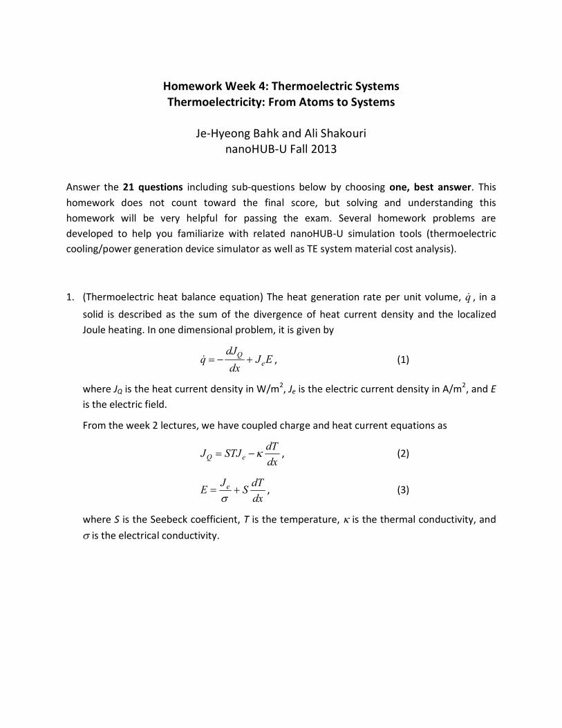
Homework Week 4: Thermoelectric Systems Thermoelectricity: From Atoms to Systems
Je-Hyeong Bahk and Ali Shakouri
nanoHUB-U Fall 2013
Answer the 21 questions including sub-questions below by choosing one, best answer. This homework does not count toward the final score, but solving and understanding this homework will be very helpful for passing the exam. Several homework problems are developed to help you familiarize with related nanoHUB-U simulation tools (thermoelectric cooling/power generation device simulator as well as TE system material cost analysis).
1. (Thermoelectric heat balance equation) The heat generation rate per unit volume, q , in a solid is described as the sum of the divergence of heat current density and the localized Joule heating. In one dimensional problem, it is given by
EJdxdJ
q eQ , (1)
where JQ is the heat current density in W/m2, Je is the electric current density in A/m2, and E is the electric field.
From the week 2 lectures, we have coupled charge and heat current equations as
dxdTSTJJ eQ , (2)
dxdTSJE e
, (3)
where S is the Seebeck coefficient, T is the temperature, is the thermal conductivity, and is the electrical conductivity.

1-1. In the steady state, the heat generation rate q becomes zero. By plugging (2) and (3) in (1), find the second derivative of temperature as a function of the material properties and the electric current density, and see how it is related to the Joule heating.
a) eJdxTd
2
2
b) eJdxTd
1
2
2
c) 22
2 1eJdx
Td
d) 22
2 1eJdx
Td
e) ee JJdxTd
2
2
2 1

1-2. (1D Temperature profile under a current flow) Now, imagine a solid of length d and cross-sectional area A as shown in the figure below. An electric current I flows in the +x direction, and a temperature gradient is created from the cold side at temperature TC to the hot side at TH.
Solve the differential equation for the second derivative of temperature obtained from the previous problem to find the one-dimensional temperature profile along the x-axis. Use the boundary condition of T(x=0) = TC, and T(x=d) = TH. I = JeA, T = TH TC, K = A/d is the thermal conductance, and R = d/(A) is the electrical resistance. Also, see how the temperature changes with x in the case of no current.
a) CTxKdRI
dTx
KdRIxT
22)(
22
2
2
b) CTxdTx
KdRIxT
2
2
2
2)(
c) CTxdTxT
)(
d) CTxKdRI
dTx
KdRIxT
22
2
2)(
e) CTxd
RIdTx
dRIxT
22)(
22
2
2

1-3. The heat dissipated to the cold side is given by the heat conduction equation as
0
out
xdx
dTAQ . (4)
Then find the heat balance equation at the cold side that depicts the balance between Qout, the Peltier cooling (= STCI), and the net cooling power QC absorbed at the cold side.
a) TKRIISTQ CC 2
b) TKRIISTQ CC 2
21
c) TKRIISTQ CC 2
21
d) TKRIISTQ CC 2
21
e) TKISTQ CC

2. (Quasi-ballistic thermoelectric cooler) Figure below shows the result of Monte Carlo simulations for carriers injected into a 3 μm-long GaAs under an applied bias of 5 kV/cm. It can be seen that it takes a distance of the order of 1 m before electrons reach equilibrium and lose energy equal to what they gain at steady state from the external electric field. Fitting the result by an exponential expression that includes an energy relaxation length E, we get the distributed Joule heating density per unit length as
Ee
xJdx
dq
exp11 2Joule . (5)
Fig. 2 Joule heating generated in the quasi-ballistic GaAs cooler as a function of distance

2-1. (Temperature profile in a quasi-ballistic cooler) Update the second derivative of temperature obtained in Problem 1-1 with Eq. (5), and then obtain the temperature profile for this quasi-ballistic thermoelectric cooler with the boundary condition of T(x=0) = TC, and T(x=d) = TH. Use the same symbols for the material properties and dimensions as in Prob. 1-2.
a) CTx
KdRI
dTx
KdRIxT
22
)(2
22
2
b) C
E
E TxdKd
RIdTx
KdRIxT
exp1
22)( 3
222
2
2
c)
E
EC
E
E xKdRITxd
KdRI
KdRI
dTx
KdRIxT
expexp
222)( 2
22
3
2222
2
2
d)
E
EC
E
E xKdRITxd
KdRI
dTx
KdRIxT
exp1exp1
22)( 2
22
3
222
2
2
e)
E
EC
E
E xKdRITxd
KdRI
KdRI
dTx
KdRIxT
exp1exp1
22)( 2
22
3
2222
2
2
f)
E
EC
E
E xKdRITxd
KdRI
KdRI
dTx
KdRIxT
exp1exp1
222)( 2
22
3
2222
2
2

2-2. (Heat dissipation at cold side) Using Eq. (4) and the temperature profile obtained in Prob. 2-1, find the heat dissipated to the cold side for the quasi-ballistic cooler.
a) TKRIQ 2out 2
1
b) TKd
RIQ E
212
out
c) TKdd
RIQ EE
22
out 21
d) TKdd
RIQE
E
exp1
21 2
2out
e) TKddd
RIQE
EE
exp1
21 2
2out
2-3. (Fraction of Joule heating dissipated to the cathode side) The heat dissipated to the cold side consists of the Joule heating term and the heat conduction term. If the length of the cooler is d = 3 μm and E is obtained from Fig. 2, what fraction of the total diffusive Joule heating (= RI2) is dissipated to the cold side? Choose the closest value.
a) 0.5
b) 0.47
c) 0.44
d) 0.41
e) 0.38

3. (Thermoelectric cooler) A thin film cooler is fabricated on top of a substrate that is much larger than the size of the thin film. An electric current can be injected from the top contact through the thin film in the cross-plane direction and then through the substrate to the ground contact. The top surface of the thin film will be cooled due to the Peltier effect.
Fig. 3 Schematic of a thin film thermoelectric cooler
3-1. (Maximum net cooling) First, imagine there is no substrate and neglect the parasitic heat conduction through the supply electrode. Use the heat balance equation obtained for a diffusive thermoelectric cooler in Problem 1-3, and find the maximum net cooling Tmax and the optimal electric current Iopt that maximizes T under an adiabatic condition at the top (cold) side, i.e. QC = 0. Use Z = S2/(RK).
a. RSTIZTT H
H opt2
max ,21
b. RSTIZTT C
C opt2
max ,21
c.
2
,22
1opt
2
maxHCHC TT
RSITTZT
d. RSTI
ZTTT H
C
H opt
2
max ,2
e. RSTI
ZTTT C
C
H opt
2
max ,2

(Prob. 3 continued) Now, run the thermoelectric device simulator on nanoHUB to check the maximum net cooling for this device. Go to the following address to reach the website for the tool, and click the ‘launch tool’ button. You may need to install JavaTM to run nanoHUB tools.
https://nanohub.org/tools/thermo
This is a screenshot of the first phase of the tool. Click the button as shown in the figure to proceed to the second phase.
In the second phase “Mode selection and Conditions”, select the first mode “Mode 1: Thermoelectric Thin Film Cooler: Cooling power is known.” Enter 0 W/cm2 for Cooling Power Density, 300 K for T ambient, Select “Current [Amp]” as an independent variable. The bottom surface of the cooler is assumed to be in contact with an ideal heat sink so that the temperature is maintained at the ambient temperature. Set “0”, “0.01”, and “2” A for Minimum value, Step value, and Maximum value of the current, respectively, as shown in the screenshot below.

Proceed to the third phase “Material Properties and Dimensions.” Set “Substrate and Spreading Effect Options” to “No Substrate.” You will see the drawing below the option changing to the no-substrate figure. Click the blue button next to the “Thin Film Properties” to enter the material property values for thin film. Enter “200” μV/K for Seebeck coefficient, “2” W/mK for thermal conductivity, “1000” (Ω-cm)-1 for electrical conductivity, “50” μm for thickness, and “10000” μm2 (100 μm x 100 μm) for Area as shown in the screenshot below:
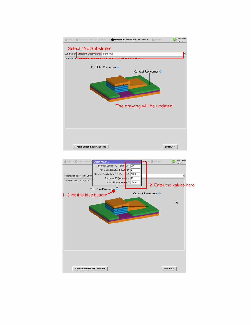

Click the second blue button for Contact Resistance, and enter “0” value for now.
Now, you are ready to run the simulation. Click the “Simulate” button to start simulation. You will get various output plots in seconds. Please note that in all of these simulations the parasitic heat conduction through the supply electrode on the cold junction is neglected.
3-2. (Simulation for maximum net cooling) What are the maximum net cooling and the current at the maximum cooling according to the simulation? Also, what are TC at the maximum cooling and Z value? Note that TC is denoted as T_1 in the simulation tool. Check if they match the calculated values from Prob. 3-1.
a. 1optmax K001.0K,6.278,A20.0,K4.21 ZTIT C
b. 1optmax K001.0K,6.264,A31.0,K4.35 ZTIT C
c. 1optmax K002.0K,6.241,A97.0,K4.58 ZTIT C
d. 1optmax K002.0K,6.215,A48.0,K4.84 ZTIT C
e. 1optmax K004.0K,6.149,A32.1,K4.150 ZTIT C

3-3. (Effect of contact resistance) Now, add a contact resistance at the interface between the top contact metal and the thin film by clicking the blue button for Contact Resistance in the second phase “Material Properties and Dimensions.” Enter “1e-6” (Ω·cm2) for Specific Contact Resistance. The total contact resistance RC is given by
ArR c
c , (6)
where rc is the specific contact resistance, and A is the cross-sectional area of the device. Note that the contact resistance is inversely proportional to the area. This contact resistance is added as an additional Joule heating in the heat balance equation at the cold side. Click “Simulate” button in the simulation tool to see the effect of contact resistance on the net cooling.
What are the maximum net cooling and the current at the maximum cooling with the contact resistance according to the simulation?
a. A24.0,K4.32 optmax IT
b. A73.0,K1.46 optmax IT
c. A97.0,K4.58 optmax IT
d. A24.1,K4.73 optmax IT
e. A42.1,K4.92 optmax IT
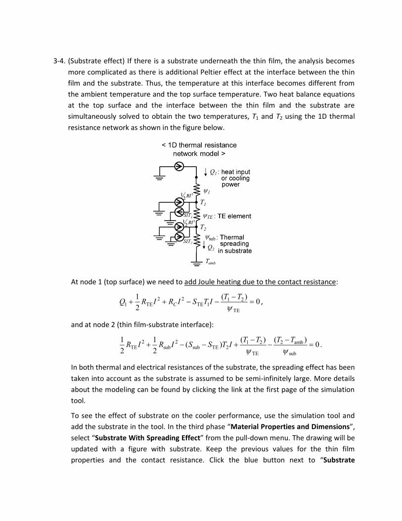
3-4. (Substrate effect) If there is a substrate underneath the thin film, the analysis becomes more complicated as there is additional Peltier effect at the interface between the thin film and the substrate. Thus, the temperature at this interface becomes different from the ambient temperature and the top surface temperature. Two heat balance equations at the top surface and the interface between the thin film and the substrate are simultaneously solved to obtain the two temperatures, T1 and T2 using the 1D thermal resistance network as shown in the figure below.
At node 1 (top surface) we need to add Joule heating due to the contact resistance:
0)(21
TE
211TE
22TE1
TTITSIRIRQ C ,
and at node 2 (thin film-substrate interface):
0)()()(21
21
sub
amb2
TE
212TEsub
2sub
2TE
TTTTITSSIRIR .
In both thermal and electrical resistances of the substrate, the spreading effect has been taken into account as the substrate is assumed to be semi-infinitely large. More details about the modeling can be found by clicking the link at the first page of the simulation tool.
To see the effect of substrate on the cooler performance, use the simulation tool and add the substrate in the tool. In the third phase “Material Properties and Dimensions”, select “Substrate With Spreading Effect” from the pull-down menu. The drawing will be updated with a figure with substrate. Keep the previous values for the thin film properties and the contact resistance. Click the blue button next to “Substrate

Properties” to enter “90” μV/K for the Seebeck coefficient, “130” W/mK for the thermal conductivity, “300” (Ωcm)-1 for the electrical conductivity, and “500” μm for the thickness of the substrate. Click the “Simulate” button to start simulation.
What are the maximum net cooling and the current at the maximum cooling with the contact resistance according to the simulation? Compare the values with the previous simulation without the substrate.
a. A24.0,K5.22 optmax IT
b. A43.0,K1.34 optmax IT
c. A69.0,K5.44 optmax IT
d. A82.0,K4.53 optmax IT
e. A94.0,K8.62 optmax IT

3-5. (Continued from Prob. 3-4) What is the temperature (T2) at the thin film-substrate interface at the maximum cooling condition? Why is T2 higher than the ambient temperature?
a. T2 = 301.9 K, because there is a Peltier heating at the interface due to the positive Seebeck value of the substrate
b. T2 = 301.9 K, because there is a Peltier heating at the interface due to the smaller Seebeck value of the substrate than that of the thin film
c. T2 = 310.9 K, because there is a Peltier heating at the interface due to the positive Seebeck value of the substrate
d. T2 = 310.9 K, because there is a Peltier heating at the interface due to the smaller Seebeck value of the substrate than that of the thin film
e. T2 = 310.9 K, because there is a Joule heating larger than the Peltier cooling at the interface.

4. (Segmented element for enhanced cooling) Two dissimilar materials can be connected in series with the same cross-sectional area to build a segmented thermoelectric element as shown in the figure below.
Ideally, if I = ST/R is satisfied at the cold side of a material, the Joule heating and the Peltier cooling cancel each other, so that the maximum cooling is obtained as you have solved it for a homogeneous material in Prob. 3-1. If the temperature variation is small, in order to have this condition satisfied at the junction between the two segmented materials, the second material needs to have a Seebeck coefficient that is twice larger than that of the first material, i.e. S2 = 2S1, so that the change in Seebeck coefficients S becomes equal to the first Seebeck coefficient S1. The Peltier cooling is proportional to S. We keep the resistances of the two segments equal. We assume the power factor, S2, to be constant throughout the device; the electrical conductivity of the second material is set to be a quarter of that of the first material.

In the thermoelectric device simulator (https://nanohub.org/tools/thermo), one can simulate such a segmented element with a thin film on a substrate that has no spreading effect. With no spreading effect, the substrate is assumed to have the same cross-sectional area as that of the thin film, so the structure mimics an element with two segments in series. In the second phase “Mode Selection and Condition” in the tool, select “Mode 1: Thermoelectric Thin Film Cooler: Cooling power is known.” Enter “0” for Cooling Power Density (this is the actual heat load at the cold junction), “300” K for T ambient, and “Current [Amp]” as an independent variable with minimum 0 A to maximum 2 A with a step of 0.01 A.

In the next phase “Material Properties and Dimensions,” select “Substrate with no spreading effect.” The drawing will be automatically updated with a shrinked substrate to the size of the thin film. Remember that we are still neglecting the parasitic heat conduction through the supply electrode on the top side. The drawing shows this electrode and the insulator region near the top segment. These are not included in the simulations but indicate some parasitic effects that should be considered in real applications.
Click the blue buttons to enter the material properties. For the first material (thin film), use Seebeck coefficient of 200 μV/K, thermal conductivity of 2 W/mK, electrical conductivity of 1000 Ω-1cm-1, thickness of 50 μm, and area of 1e4 μm2. For the second material (substrate), use Seebeck coefficient of 400 μV/K, thermal conductivity of 2 W/mK, electrical conductivity of 250 Ω-1cm-1, and thickness of 12.5 μm. Leave the contact resistance to be “0”. Then click “Simulate” to start the simulation.

After the simulation is done, find the maximum cooling, Tmax. Calculate ½ZTC2 in this case
using the cold side temperature Tc obtained from the simulation, and the material properties. See that the maximum cooling was enhanced from ½ZTC
2 with the additional segment made of the second material at the hot side.
a. K38.5821,K57.41 2
max CZTT
b. K38.5821,K82.54 2
max CZTT
c. K0.5221,K97.71 2
max CZTT
d. K0.5221,K97.76 2
max CZTT
e. K04.4821,K27.88 2
max CZTT

5. (Thermoelectric power generator) The same geometry of a thermoelectric device can be used as a power generator when the top surface is heated and substrate heat sunk to create temperature gradient across the device and generate a Seebeck voltage. When a load resistance RL is connected to the power generator, a power is generated at the load by current flow as the thermoelectric device acts as a voltage supplier.
Fig. 3 Schematic of a thin film thermoelectric power generator
5-1. (Power output) First, imagine there is no substrate. What are the electrical current and the power generated at the load if the top surface temperature is TH, the bottom temperature is TC, S is the Seebeck coefficient, and R is the electrical resistance of the power generator? (we neglect heat conduction through the supply electrode as well as Joule heating in the wires).
a. 2
22
out,R
RTSPRTTSI LCH
b. LL
CH
RTSP
RTTSI
22
out,
c. 2
22
out,L
LH
L
H
RRRTSP
RRSTI
d. 2
22
out,L
LC
L
C
RRRTSP
RRSTI
e. 2
22
out,L
L
L
CH
RRRTSP
RRTTSI

5-2. (Maximum power output) What is the load resistance that maximizes the power output, and what is the maximum power output? (Hint: Differentiate Pout found in Prob. 5-1 with respect to RL.)
a. 2
22
maxout, )1(4,
HHL ZTR
TSPRZTR
b. )1(4
,122
maxout,H
HL ZTRTSPZTRR
c. 2
22
maxout, )1(4,1
HHL ZTR
TSPZTRR
d. RTSPRRL 4
,22
maxout,
e. RTSPRRL 9
,222
maxout,
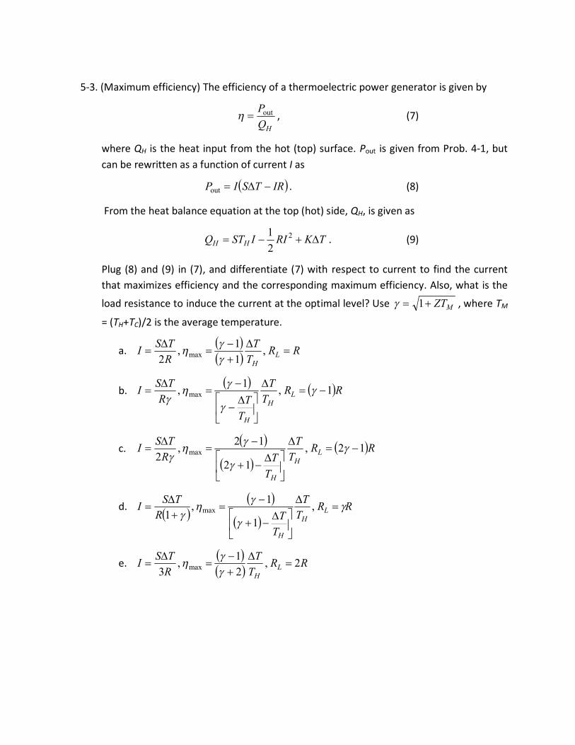
5-3. (Maximum efficiency) The efficiency of a thermoelectric power generator is given by
HQ
Pout , (7)
where QH is the heat input from the hot (top) surface. Pout is given from Prob. 4-1, but can be rewritten as a function of current I as
IRTSIP out . (8)
From the heat balance equation at the top (hot) side, QH, is given as
TKRIISTQ HH 2
21
. (9)
Plug (8) and (9) in (7), and differentiate (7) with respect to current to find the current that maximizes efficiency and the corresponding maximum efficiency. Also, what is the
load resistance to induce the current at the optimal level? Use MZT 1 , where TM
= (TH+TC)/2 is the average temperature.
a. RR
TT
RTSI L
H
,11,
2 max
b. RRTT
TTR
TSI LH
H
1,1, max
c.
RR
TT
TTR
TSI LH
H
12,12
12,2 max
d.
RR
TT
TTR
TSI LH
H
,1
1,1 max
e. RR
TT
RTSI L
H2,
21,
3 max

5-4. (Carnot limit of efficiency) What ZTM value is needed to have the maximum efficiency equal to the Carnot efficiency, ηcarnot = T/TH?
a. 1MZT
b. 0MZT
c. 10MZT
d. 100MZT
e. MZT
5-5. (Simulation for maximum power output) Use the thermoelectric device simulation tool (https://nanohub.org/tools/thermo) to simulate the performance of a thermoelectric power generator. Clear the previous output plots by clicking “clear” at the output page if necessary.
In the pull-down menu in the second phase “Mode Selection and Conditions,” select “Mode 4: Thermoelectric Thin Film Power Generator: Top temperature is known.” Enter “600” K for Temperature 1, “300” K for ambient temperature, “Load Resistance [Ohm]” as an independent variable, and “0”, “1e-4”, and “0.3” Ω for Minimum Value, Step Value, and Maximum Value of the load resistance, respectively.
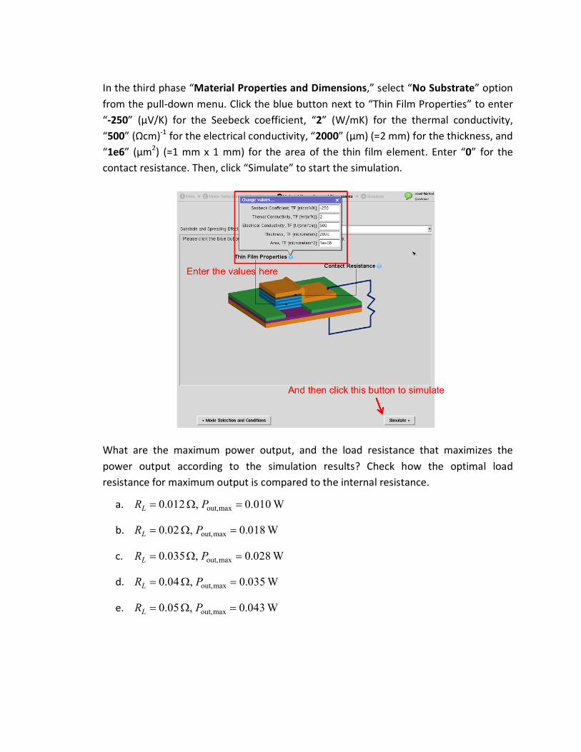
In the third phase “Material Properties and Dimensions,” select “No Substrate” option from the pull-down menu. Click the blue button next to “Thin Film Properties” to enter “-250” (μV/K) for the Seebeck coefficient, “2” (W/mK) for the thermal conductivity, “500” (Ωcm)-1 for the electrical conductivity, “2000” (μm) (=2 mm) for the thickness, and “1e6” (μm2) (=1 mm x 1 mm) for the area of the thin film element. Enter “0” for the contact resistance. Then, click “Simulate” to start the simulation.
What are the maximum power output, and the load resistance that maximizes the power output according to the simulation results? Check how the optimal load resistance for maximum output is compared to the internal resistance.
a. W010.0,012.0 maxout, PRL
b. W018.0,02.0 maxout, PRL
c. W028.0,035.0 maxout, PRL
d. W035.0,04.0 maxout, PRL
e. W043.0,05.0 maxout, PRL
5-6. (Maximum efficiency, continued from Prob. 4-4) What is the maximum efficiency, and the load resistance for that maximum efficiency according to the previous simulation results? Check how the optimal load resistance for maximum efficiency is compared to the internal resistance.
a. 027.0,012.0 max LR
b. 041.0,024.0 max LR
c. 052.0,032.0 max LR
d. 690.0,044.0 max LR
e. 850.0,052.0 max LR

5-7. (Simulation on Power output as a function of temperature difference) Now, simulate the power output as a function of the temperature difference T. Click “clear” at the down right corner at the output page to clear the previous simulation results. Go back to the second phase “Mode Selection and Conditions”, and leave the mode to be “Mode 4: Thermoelectric Thin Film Power Generator.” Change the independent variable to “Temperature 1 [K].” Set the minimum, step, and maximum values of the temperature 1 to be “300”, “10”, and “600” K, respectively. Leave the ambient temperature to be “300” K. Enter “0.04” Ω for the load resistance. Note that this load resistance value matches the internal resistance of the power generator.
Keep the previous material property and dimension values as used in the previous simulation in the third phase. Click “Simulate” to start the simulation.

After the simulation is done, check the power output graph as a function of the top surface temperature (T1). What are the power outputs at T1 = 400 K, 500 K, and 600K, respectively? See if the power output increases in proportion to (T)2 as predicted in Prob. 5-2.
a. mW8.10 and,8.4,2.1out P
b. mW7.20 and,2.9,3.2out P
c. mW2.35 and,6.15,9.3out P
d. mW5.40 and,0.18,5.4out P
e. mW8.46 and,8.20,2.5out P

6. (Thermoelectric system optimization) A thermoelectric energy conversion module consists of multiple pairs of n-type and p-type elements connected electrically in series, and placed in parallel along the heat flow direction. One side of the module is attached to a heat source via a heat exchanger to ensure high heat transfer between them. The other side of the module is attached to a heat sink to create a large temperature gradient across the module. This whole thermoelectric energy conversion system needs to be optimized together with both-side heat exchangers.
Fig. 6 A thermoelectric energy conversion system with heat exchangers
The analysis and optimization is complicated, so we have built another simulation tool on nanoHUB for the performance optimization of a thermoelectric system. Go to the following link to launch the system optimization tool:
https://nanohub.org/tools/tedev
Click “Launch Tool” on the website to launch the tool. Read the introduction page in the tool carefully. This tool finds the optimal thickness of the thermoelectric elements and the optimal load resistance by co-optimizing the thermal and electrical resistances of the thermoelectric module with given material properties of the thermoelectric elements, and the heat transfer coefficients of the heat exchangers, and calculates the maximum power output and cost of the system.

In the case of the symmetric thermal resistances at hot and cold sides, the maximum power output per unit area is given by
22max1
)11(4 aSM
TTAZT
ZP
, (10)
where A is the substrate area, ∑Ψ is the sum of the external thermal resistances including heat exchangers and spreading thermal resistances in the substrates, TS is the heat source temperature, and Ta is the ambient temperature. Note that as we change the number of n- and p-legs without changing the area covered by TE material, we trade off the generated voltage and the current but the power output of the TE module per unit area does not change.
In the second phase named “Simulation Options,” one can vary either one of the material properties such as Seebeck coefficient, electrical conductivity and thermal conductivity of the thermoelectric material used, or a heat transfer coefficient at hot or cold side to study the variation of the maximum power output and cost per Watt as a function of the independent variable.
6-1. (Power output) First, choose “Power Output as a function of Material Properties” in the topmost pull-down menu in the second phase. Then choose “Thermal Conductivity” as an independent variable in the second pull-down menu. Enter “0.5” W/mK for the initial value of thermal conductivity, “3.0” W/mK for the final value, and “0.1” W/mK for increment. Set the Seebeck coefficient at “300” μV/K , and the electrical conductivity at “370” Ω-1cm-1. For both heat transfer coefficients at the hot and cold sides, use “400” W/m2K.

In the next phase named “Fixed Parameters”, check the set values for the other parameters describing system conditions, dimensions and cost information of the thermoelectric system to simulate. These set values are realistic values obtained from a steam turbine environment. Among them, note that the fractional area coverage, or fill factor is set to 0.1, meaning that only 10 % of the substrate area is covered by the thermoelectric elements. We will keep the set values for the parameters during the simulations. Click “Simulate” button to start the simulation.
Once the simulation is done, check the output graphs. Then, do not clear the output plots and go back to the second phase “Simulation Options.” Now, choose “Seebeck coefficient” as an independent variable, and vary from “100” μV/K to “500” μV/K with “10” μV/K increment. Set the thermal conductivity at “1.5” W/mK, and the electrical conductivity at “370” Ω-1cm-1. Keep both heat transfer coefficients at “400” W/m2K. Click “Simulate” to start the simulation.

Once the simulation is done, do not clear the output plots again and go back to the second phase “Simulation Options.” Now, choose “Electrical Conductivity” as an independent variable, and vary from “100” Ω-1cm-1 to “1000” Ω-1cm-1 with “10” Ω-1cm-1 increment. Set the thermal conductivity at “1.5” W/mK, and the Seebeck coefficient at “300” μV/K. Keep both heat transfer coefficients at “400” W/m2K. Click “Simulate” to start the simulation.

Now, you have collected all the graphs for the three simulations in the output page. Choose the “Power Output vs. ZT” graph from the pull-down menu in the output page. See how the power output changes with varying different material properties.
Repeat the three simulations done so far with different values of the hot and cold-side heat transfer coefficients of “200” W/m2K. Then, repeat the three simulations again with “600” W/m2K for the two heat transfer coefficients. Learn how the power output changes with varying all the heat transfer coefficients and the material properties. Pay particular attention to “Power Output vs. ZT” plots. Be careful with the graphs plotted together in a plot with different x-axes. You can turn on and off some of the curves using the legend sidebar on the right side, and zoom in and out with your mouse on a plot.

After all these simulations, which of the following statements is correct about the power output of this thermoelectric system?
a. The higher the heat transfer coefficient is, the lower the power output is generated.
b. Optimal power output is only a function of the heat transfer coefficients, and not of the material properties.
c. Optimal power output does not change with varying any of the three individual material properties and the heat transfer coefficients as long as the ZT value remains the same.
d. Optimal power output does not change with varying any of the three individual material properties as long as the ZT value and the heat transfer coefficients remain the same.
e. None of the above.

6-2. (Cost analysis) Now, choose “Power Cost vs. ZT” graph among the output plots. Open the legend sidebar by clicking the blue arrowed button on the right hand side of the plot. Deselect all other curves, leaving only the first three simulation curves selected. These curves are the ones with the constant heat transfer coefficients of 400 W/m2K while varying the three material properties.
After carefully looking at the three remaining curves, find a correct statement among the followings.
a. Materials produce the same power cost if their ZT values are the same.
b. In the high ZT regime (e.g. ZT higher than ~ 3.0), lowering the thermal conductivity is more desired than enhancing the power factor in terms of power cost if ZT remains the same.
c. In the high ZT regime (e.g. ZT higher than ~ 3.0), enhancing the power factor is more desired than lowering the thermal conductivity in terms of power cost if ZT remains the same.
d. Power cost increases with increasing ZT.
e. Power cost decreases with decreasing efficiency.