Embed Size (px)
Citation preview
PROPRIETARY NOTETHIS SPECIFICATION IS THE PROPERTY OF BOE DT AND SHALL NOT BEREPRODUCED OR COPIED WITHOUT THE WRITTEN PERMISSION OF BOE DT AND MUST BE RETURNED TO BOE DT UPON ITS REQUEST
HM215WU1 500 ProductHM215WU1-500 Product
Specification Rev.P2
BEIJING BOE DISPLAY TECHNOLOGY
A4(210 X 297)
SPEC. NUMBERSPRODUCT GROUP Rev.P2 ISSUE DATE
2013.11.19
PAGE
A4(210 X 297)
PAGE
OF 30
B2010-8002-O (1/3)
1TFT-LCD

REVISION HISTORY
PRODUCT GROUP REV ISSUE DATE
TFT- LCD PRODUCT Rev.P2 Nov.19. 13’
REV. ECN No. DESCRIPTION OF CHANGES DATE PREPARED
Rev.P0 Initial Release May.10. 13’ Wang Hetao
Rev.P1 2nd Release Sep. 25. 13’ Wang Hetao
Rev P2 3rd Release Nov 19 13’ Wang Hetao
REVISION HISTORY
Rev.P2 3rd Release Nov.19.13 Wang Hetao
B2010-8002-O (2/3) A4(210 X 297)
SPEC. NUMBER
S
SPEC. TITLE
HM215WU1-500 Product Specification_Rev.P2
PAGE
OF 302
REV ISSUE DATEPRODUCT GROUP
Rev.P2TFT- LCD PRODUCT Nov. 19. 13’
C t tContents
No. Item Page
1.0 General Description 4
2.0 Absolute Maximum Ratings 6
3.0 Electrical Specifications 7
4.0 Optical Specifications 9
5.0 Interface Connection 11
6.0 Signal Timing Specifications 15
7 0 Signal Timing Waveforms of Interface Signal 167.0 Signal Timing Waveforms of Interface Signal 16
8.0 Input Signals, Display Colors & Gray Scale of Colors 19
9.0 Power Sequence 20
10.0 Mechanical Characteristics 21
11.0 Reliability Test 22
12.0 Handling& Cautions 23
13.0 Product Serial Number 24
14.0 Packing 25
15.0 Appendix 27
A4(210 X 297)
PAGE
OF 30SPEC. NUMBER
S
SPEC. TITLE
HM215WU1-500 Product Specification_Rev.P2
B2010-8002-O (3/3)
3
REV ISSUE DATEPRODUCT GROUP
Rev.P2TFT- LCD PRODUCT Nov. 19. 13’
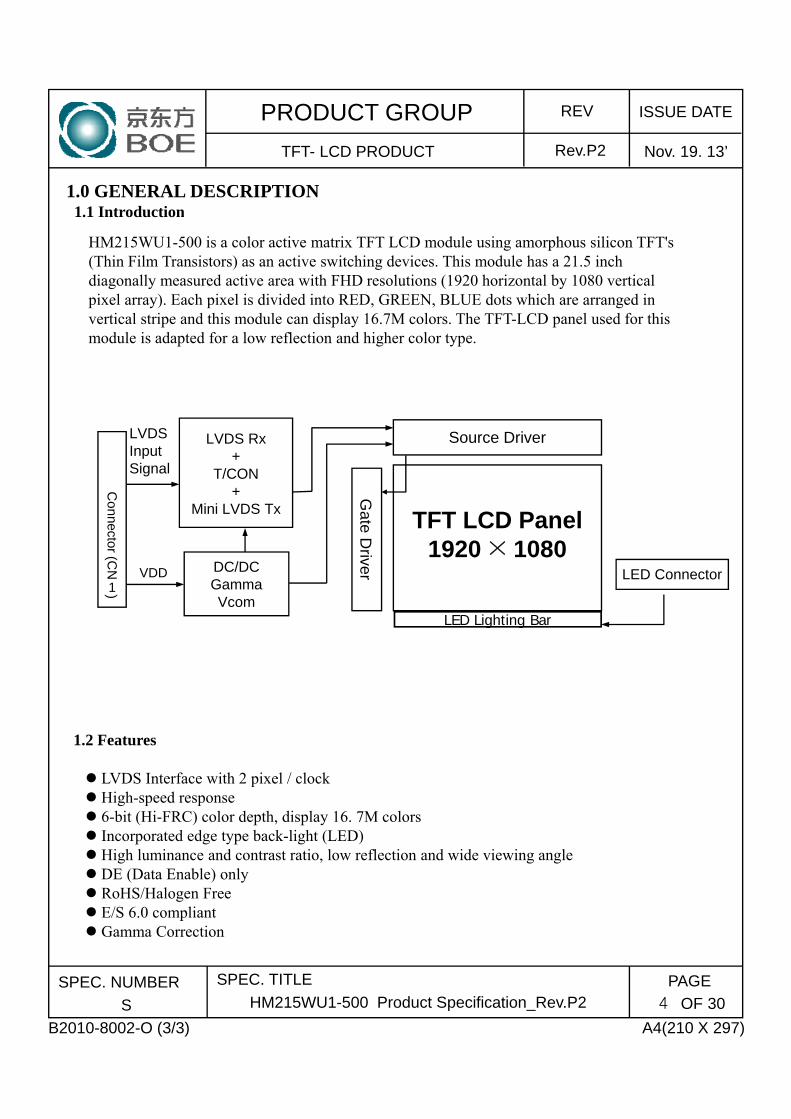
1.0 GENERAL DESCRIPTION1.1 Introduction
HM215WU1-500 is a color active matrix TFT LCD module using amorphous silicon TFT's (Thin Film Transistors) as an active switching devices. This module has a 21.5 inch diagonally measured active area with FHD resolutions (1920 horizontal by 1080 vertical pixel array). Each pixel is divided into RED, GREEN, BLUE dots which are arranged in vertical stripe and this module can display 16.7M colors. The TFT-LCD panel used for this module is adapted for a low reflection and higher color type.
1.1 Introduction
Source DriverLVDS Rx+
T/CON+
LVDSInputSignal
Gate D
river
TFT LCD Panel1920 × 1080
+Mini LVDS Tx
DC/DCGammaVcom
Connector (C
N
1)
VDD
LED Lighting Bar
LED Connector
1.2 Features
g g
LVDS Interface with 2 pixel / clock High-speed response 6-bit (Hi-FRC) color depth, display 16. 7M colors Incorporated edge type back-light (LED) High luminance and contrast ratio, low reflection and wide viewing angle DE (Data Enable) only RoHS/Halogen Free
A4(210 X 297)
PAGE
OF 30SPEC. NUMBER
S
SPEC. TITLE
HM215WU1-500 Product Specification_Rev.P2
B2010-8002-O (3/3)
4
g E/S 6.0 compliant Gamma Correction
REV ISSUE DATEPRODUCT GROUP
Rev.P2TFT- LCD PRODUCT Nov. 19. 13’
1.3 Application
Desktop Type of PC & Workstation Use Slim-Size Display for Stand-alone Monitor Display Terminals for Control SystemMonitors for Process Controller
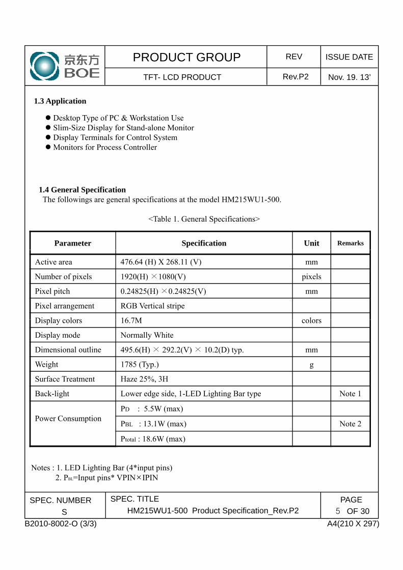
1.4 General SpecificationThe followings are general specifications at the model HM215WU1-500.
<Table 1. General Specifications>
Parameter Specification Unit Remarks
Active area 476.64 (H) X 268.11 (V) mm
Number of pixels 1920(H) ×1080(V) pixels
Pixel pitch 0.24825(H) ×0.24825(V) mm
Pixel arrangement RGB Vertical stripe
Display colors 16 7M colorsDisplay colors 16.7M colors
Display mode Normally White
Dimensional outline 495.6(H) × 292.2(V) × 10.2(D) typ. mm
Weight 1785 (Typ.) g
Surface Treatment Haze 25%, 3H
Back-light Lower edge side, 1-LED Lighting Bar type Note 1
Power ConsumptionPD : 5.5W (max)
PBL : 13.1W (max) Note 2
Ptotal : 18.6W (max)
A4(210 X 297)
PAGE
OF 30SPEC. NUMBER
S
SPEC. TITLE
HM215WU1-500 Product Specification_Rev.P2
B2010-8002-O (3/3)
5
Notes : 1. LED Lighting Bar (4*input pins)2. PBL=Input pins* VPIN×IPIN
REV ISSUE DATEPRODUCT GROUP
Rev.P2TFT- LCD PRODUCT Nov. 19. 13’
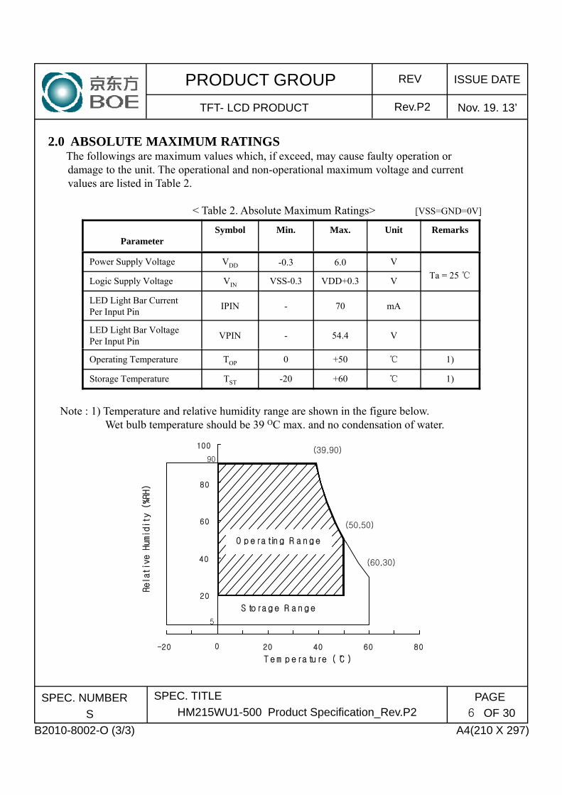
2.0 ABSOLUTE MAXIMUM RATINGSTh f ll i i l hi h if d f lt tiThe followings are maximum values which, if exceed, may cause faulty operation or damage to the unit. The operational and non-operational maximum voltage and current values are listed in Table 2.
< Table 2. Absolute Maximum Ratings> [VSS=GND=0V]
ParameterSymbol Min. Max. Unit Remarks
Power Supply Voltage VDD -0.3 6.0 V
Ta = 25 Logic Supply Voltage VIN VSS-0.3 VDD+0.3 V
LED Light Bar CurrentPer Input Pin
IPIN - 70 mA
LED Light Bar VoltagePer Input Pin
VPIN - 54.4 V
Operating Temperature TOP 0 +50 1)
Storage Temperature TST -20 +60 1)
Note : 1) Temperature and relative humidity range are shown in the figure below.Wet bulb temperature should be 39 OC max. and no condensation of water.
100
60
80
90
100
O p e ra tin g R a n g eumid
ity
(%RH
)
(39,90)
(50,50)
5
20
40
O p e ra tin g R a n g e
S to ra g e R a n g e
Rela
tive
Hu
(60,30)
A4(210 X 297)
PAGE
OF 30SPEC. NUMBER
S
SPEC. TITLE
HM215WU1-500 Product Specification_Rev.P2
B2010-8002-O (3/3)
6
0 20 40 60 80-20
T e m p e ra tu re ( C )
REV ISSUE DATEPRODUCT GROUP
Rev.P2TFT- LCD PRODUCT Nov. 19. 13’
3.0 ELECTRICAL SPECIFICATIONS3.1Electrical Specifications
[ 2 ±2 ]< Table 3. Electrical specifications >
Parameter Min. Typ. Max. Unit Remarks
Power Supply Voltage VDD 4.5 5.0 5.5 VNote1
Power Supply Current IDD - 900 1100 mA
In-Rush Current IRUSH - 2.0 3.0 A Note 2
Permissible Input Ripple Voltage VRF - - 300 mV Note3
[Ta =25±2 ]
p pp g RF
High Level Differential Input Threshold Voltage
VIH - - +100 mV
Low Level Differential Input Threshold Voltage
VIL -100 - - mV
Differential input voltage |VID | 200 - 600 mV
Differential input common mode voltage Vcm 1.0 1.2 1.5VIH=100mV,VIL=-100mVVIL 100mV
Power Consumption
PD - 3.5 5.5 W
PBL 11.1 12.3 13.1 W Note 4
Ptotal - 15.8 18.6 W
Notes : 1. The supply voltage is measured and specified at the interface connector of LCM.The current draw and power consumption specified is for VDD=5.0V, Frame rate=75HzThe current draw and power consumption specified is for VDD 5.0V, Frame rate 75HzClock frequency = 92.9 MHz. Test Pattern of power supply current
a) Typ : Color Testb) Max : Skip Subpixel255
2. Duration of rush current is about 2 ms and rising time of VDD is 520 μs ± 20 %3 i ibl i l l h ld b d d 0 2 °C f (f f ) A3. Permissible Input ripple Voltage should be measured under VDD =5.0V, 25°C, fV(frame frequency)=MAX
condition(@ Gray level 255 Gray level 0) and At that time, we recommend the bandwidth configuration ofoscilloscope is to be under 20Mhz. Ripple Voltage should be covered by Input voltage Spec.
4. Calculated value for reference (Input pins*VPIN ×IPIN) excluding inverter loss.
A4(210 X 297)
PAGE
OF 30SPEC. NUMBER
S
SPEC. TITLE
HM215WU1-500 Product Specification_Rev.P2
B2010-8002-O (3/3)
7
Gray level 255 Gray level 0
REV ISSUE DATEPRODUCT GROUP
Rev.P2TFT- LCD PRODUCT Nov. 19. 13’
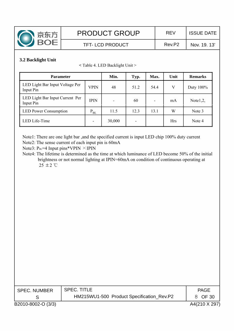
3.2 Backlight Unit T bl 4 LED B kli ht U it
Parameter Min. Typ. Max. Unit Remarks
LED Light Bar Input Voltage Per Input Pin
VPIN 48 51.2 54.4 V Duty 100%
LED Light Bar Input Current Per Input Pin
IPIN - 60 - mA Note1,2,
< Table 4. LED Backlight Unit >
p
LED Power Consumption PBL 11.5 12.3 13.1 W Note 3
LED Life-Time - 30,000 - Hrs Note 4
Note1: There are one light bar ,and the specified current is input LED chip 100% duty current Note2: The sense current of each input pin is 60mANote3: PBL=4 Input pins*VPIN ×IPINNote4: The lifetime is determined as the time at which luminance of LED become 50% of the initial
brightness or not normal lighting at IPIN=60mA on condition of continuous operating at 25 ±2
A4(210 X 297)
PAGE
OF 30SPEC. NUMBER
S
SPEC. TITLE
HM215WU1-500 Product Specification_Rev.P2
B2010-8002-O (3/3)
8
REV ISSUE DATEPRODUCT GROUP
Rev.P2TFT- LCD PRODUCT Nov. 19. 13’
4.0 OPTICAL SPECIFICATION4 1 O i4.1 Overview
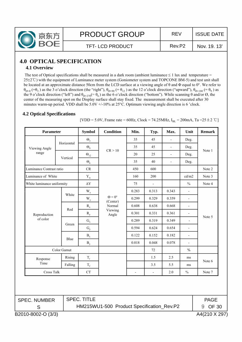
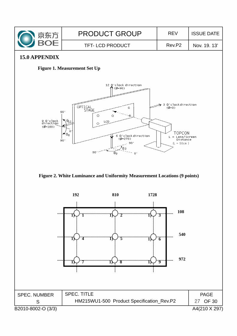
The test of Optical specifications shall be measured in a dark room (ambient luminance 1 lux and temperature = 252) with the equipment of Luminance meter system (Goniometer system and TOPCONE BM-5) and test unit shall be located at an approximate distance 50cm from the LCD surface at a viewing angle of θ and Φ equal to 0. We refer to θØ=0 (=θ3 ) as the 3 o’clock direction (the “right”), θØ=90 (= θ12 ) as the 12 o’clock direction (“upward”), θØ=180 (= θ9 ) as the 9 o’clock direction (“left”) and θØ=270(= θ6 ) as the 6 o’clock direction (“bottom”). While scanning θ and/or Ø, the center of the measuring spot on the Display surface shall stay fixed. The measurement shall be executed after 30 minutes warm-up period. VDD shall be 5.0V +/-10% at 25C. Optimum viewing angle direction is 6 ’clock.
Parameter Symbol Condition Min. Typ. Max. Unit Remark
Viewing Angle
HorizontalΘ3
CR > 10
35 45 - Deg.
N t 1Θ9 35 45 - Deg.
4.2 Optical Specifications[VDD = 5.0V, Frame rate = 60Hz, Clock = 74.25MHz, IBL = 200mA, Ta =25±2 ]
g grange
CR > 10 Note 1
VerticalΘ12 20 25 - Deg.
Θ6 35 40 - Deg.
Luminance Contrast ratio CR 450 600 Note 2
Luminance of White Yw 160 200 cd/m2 Note 3
White luminance uniformity ΔY 75 - % Note 4
W 0 283 0 313 0 343 -
Θ = 0(Center)Normal Viewing AngleReproduction
of color
WhiteWx 0.283 0.313 0.343
Note 5
Wy 0.299 0.329 0.359 -
RedRx 0.608 0.638 0.668 -
Ry 0.301 0.331 0.361 -
GreenGx 0.289 0.319 0.349 -
Gy 0.594 0.624 0.654 -
BlueBx 0.122 0.152 0.182 -
By 0.018 0.048 0.078 -
Color Gamut 72 %
ResponseTime
Rising Tr 1.5 2.5 msNote 6
Falling Tf 3.5 5.5 ms
Cross Talk CT - - 2.0 % Note 7
A4(210 X 297)
PAGE
OF 30SPEC. NUMBER
S
SPEC. TITLE
HM215WU1-500 Product Specification_Rev.P2
B2010-8002-O (3/3)
9
REV ISSUE DATEPRODUCT GROUP
Rev.P2TFT- LCD PRODUCT Nov. 19. 13’
1. Viewing angle is the angle at which the contrast ratio is greater than 10. The viewing are determined for the horizontal or 3, 9 o’clock direction and the vertical or 6, 12 o’clock direction with respect to the optical axis which is normal to the LCD surface.
2. Contrast measurements shall be made at viewing angle of = 0 and at the center of the LCD surface. Luminance shall be measured with all pixels in the view field set first to white, then
h d k (bl k) (S FIGURE 1 h i A di ) L i C R i (CR)
Note :
to the dark (black) state. (See FIGURE 1 shown in Appendix) Luminance Contrast Ratio (CR) is defined mathematically.
Luminance when displaying a white rasterLuminance when displaying a black raster
3. Center Luminance of white is defined as the LCD surface. Luminance shall be measured with ll i l i th i fi ld t fi t t hit Thi t h ll b t k t th l ti
CR =
all pixels in the view field set first to white. This measurement shall be taken at the locations shown in FIGURE 2 for a total of the measurements per display.
4. The White luminance uniformity on LCD surface is then expressed as :ΔY = ( Minimum Luminance of 9points / Maximum Luminance of 9points ) * 100 (See FIGURE 2 shown in Appendix).
5. The color chromaticity coordinates specified in Table 4. shall be calculated from the spectral data measured with all pixels first in red, green, blue and white. Measurements shall be made at the center of the panelat the center of the panel.
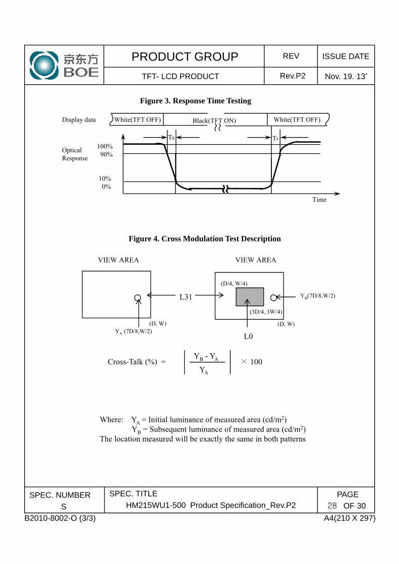
6. The electro-optical response time measurements shall be made as FIGURE 3 shown in Appendix by switching the “data” input signal ON and OFF. The times needed for the luminance to change from 10% to 90% is Td, and 90% to 10% is Tr.
7. Cross-Talk of one area of the LCD surface by another shall be measured by comparing the luminance (YA) of a 25mm diameter area, with all display pixels set to a gray level, to the luminance (YB) of that same area when any adjacent area is driven dark. (See FIGURE 4 shown in Appendix)shown in Appendix).
A4(210 X 297)
PAGE
OF 30SPEC. NUMBER
S
SPEC. TITLE
HM215WU1-500 Product Specification_Rev.P2
B2010-8002-O (3/3)
10
REV ISSUE DATEPRODUCT GROUP
Rev.P2TFT- LCD PRODUCT Nov. 19. 13’
5.0 INTERFACE CONNECTION.5 1 El t i l I t f C ti5.1 Electrical Interface Connection
5.1.1 LED Light Bar
Pin No Symbol Description
1 IRLED1 LED current sense for string1
2 IRLED2 LED current sense for string2
< Table 1. LED Light Bar>
2 IRLED2 LED current sense for string2
3 VLED LED power supply
4 VLED LED power supply
5 IRLED3 LED current sense for string3
6 IRLED4 LED current sense for string4
7 CONNECTOR 3708K-Q06N-00R7 CONNECTOR 3708K Q06N 00R
Figure1. Top View of LED Bar Connector
A4(210 X 297)
PAGE
OF 30SPEC. NUMBER
S
SPEC. TITLE
HM215WU1-500 Product Specification_Rev.P2
B2010-8002-O (3/3)
11
Figure2. Back Side of Module
REV ISSUE DATEPRODUCT GROUP
Rev.P2TFT- LCD PRODUCT Nov. 19. 13’
5.0 INTERFACE CONNECTION.5 1 El t i l I t f C ti5.1 Electrical Interface Connection
CN11 Module Side Connector : UJU IS100-L30R-C23or EquivalentUser Side Connector : JAE FI-X30H or Equivalent
Pin No Symbol Function Remark
1 RXO0- Negative Transmission data of Pixel 0 (ODD)
2 RXO0+ Positive Transmission data of Pixel 0 (ODD)2 RXO0+ Positive Transmission data of Pixel 0 (ODD)
3 RXO1- Negative Transmission data of Pixel 1 (ODD)
4 RXO1+ Positive Transmission data of Pixel 1 (ODD)
5 RXO2- Negative Transmission data of Pixel 2 (ODD)
6 RXO2+ Positive Transmission data of Pixel 2 (ODD)
7 GND Power Ground
8 RXOC- Negative Transmission Clock (ODD)
9 RXOC+ P iti T i i Cl k (ODD)9 RXOC+ Positive Transmission Clock (ODD)
10 RXO3- Negative Transmission data of Pixel 3 (ODD)
11 RXO3+ Positive Transmission data of Pixel 3 (ODD)
12 RXE0- Negative Transmission data of Pixel 0 (EVEN)
13 RXE0+ Positive Transmission data of Pixel 0 (EVEN)
14 GND Power Ground
15 RXE1- Negative Transmission data of Pixel 1 (EVEN)
16 RXE1 P i i T i i d f Pi l 1 (EVEN)16 RXE1+ Positive Transmission data of Pixel 1 (EVEN)
17 GNG Power Ground
18 RXE2- Negative Transmission data of Pixel 2 (EVEN)
19 RXE2+ Positive Transmission data of Pixel 2 (EVEN)
20 RXEC- Negative Transmission Clock (EVEN)
21 RXEC+ Positive Transmission Clock (EVEN)
22 RXE3- Negative Transmission data of Pixel 3 (EVEN)
23 RXE3+ Positive Transmission data of Pixel 3 (EVEN)
24 GND Power Ground Note 1
25 NC
No. Connection26 NC
27 NC
28 VDD
Power Supply: +5V29 VDD
A4(210 X 297)
PAGE
OF 30SPEC. NUMBER
S
SPEC. TITLE
HM215WU1-500 Product Specification_Rev.P2
B2010-8002-O (3/3)
12
30 VDD
Note 1 : This pin should be connected with GND.
REV ISSUE DATEPRODUCT GROUP
Rev.P2TFT- LCD PRODUCT Nov. 19. 13’
5.2 LVDS Interface (Tx; THC63LVDF83A or Equivalent)5 2 1 LVDS Interface5.2.1 LVDS Interface
Pin No.
HT236F01-100 (CN11)
TFT-LCD (Rx)
Pin No. System (Tx)
Interface
Pin No.
52
51
Transmitter Remark
OR1
OR0
InputSignal
12
RXO0-RXO0+
4847
OUT0-OUT0+
7
6
4
3
56
55
54
OG2
OG1
OG0
OR5
OR4
OR3
OR2
34
RXO1-RXO1+
4645
OUT1-OUT1+
22
20
19
15
14
12
11
OB3
OB2
OB1
OB0
OG5
OG4
OG3
LVD
89
56
RXO CLK-RXO CLK+
RXO2-RXO2+
4039
4241
CLK OUT-CLK OUT+
OUT2-OUT2+
31
30
28
27
24
23
22
MCLK
DE
Vsync
Hsync
OB5
OB4
OB3DS
1011
RXO3-RXO3+
3837
OUT3-OUT3+
25
18
16
10
8
2
50
RSVD
OB7
OB6
OG7
OG6
OR7
OR6
A4(210 X 297)
PAGE
OF 30SPEC. NUMBER
S
SPEC. TITLE
HM215WU1-500 Product Specification_Rev.P2
B2010-8002-O (3/3)
13
25RSVD

REV ISSUE DATEPRODUCT GROUP
Rev.P2TFT- LCD PRODUCT Nov. 19. 13’
5.3 Data Input Format
(1,1) (2,1) (1919,1) (1920,1)
R G B R G B R G B R G BR G B R G B R G B R G B
1 Pixel = 3 Dots
R G B
R G B R G B R G B R G B
(1,1080) (2,1080) (1919,1080) (1920,1080)Display Position of Input Data (V H)Display Position of Input Data (V-H)
A4(210 X 297)
PAGE
OF 30SPEC. NUMBER
S
SPEC. TITLE
HM215WU1-500 Product Specification_Rev.P2
B2010-8002-O (3/3)
14

REV ISSUE DATEPRODUCT GROUP
Rev.P2TFT- LCD PRODUCT Nov. 19. 13’
6.0 SIGNAL TIMING SPECIFICATION6 1 Th HM215WU1 500 i t d b th DE l6.1 The HM215WU1-500 is operated by the DE only.
Item Symbols Min Typ Max Unit
Clock
Frequency 1/Tc 58.54 74.25 98 MHz
High Time Tch - 3/7Tc -
Low Time Tcl - 3/7Tc -
Frame Period Tv
1115 1126 1136 lines
50 60 75 Hz
20 16.7 13.3 ms
Vertical Display Period Tvd - 1080 - lines
One line Scanning Period Th 1050 1100 1150 clocks
Horizontal Display Period Thd 960 960 960 clocks
Modulating frequency of input clock
d i SSC
Flvmod 10 - 200 KHz
F=85MHzVic=1.2V
Vid=±200mV
during SSC
Maximum deviation of input clock
frequency during SSC
Flvdev -3 - +3 %
Cycle to200
Cycle to Cycle jitter
Tcy-cy - - 200 ps
A4(210 X 297)
PAGE
OF 30SPEC. NUMBER
S
SPEC. TITLE
HM215WU1-500 Product Specification_Rev.P2
B2010-8002-O (3/3)
15

REV ISSUE DATEPRODUCT GROUP
Rev.P2TFT- LCD PRODUCT Nov. 19. 13’
6.2 LVDS Rx Interface Timing ParameterThe specification of the LVDS Rx interface timing parameter is shown in Table 4The specification of the LVDS Rx interface timing parameter is shown in Table 4.
<Table 4. LVDS Rx Interface Timing Specification>
Item Symbol Min Typ Max Unit Remark
CLKIN Period tRCIP 10.20 13.47 17.08 nsec
Input Data 0 tRIP1 -0.4 0.0 +0.4 nsec
I t D t 1 tRIP0 tRCIP/7 0 4 tRCIP/7 tRCIP/7+0 4Input Data 1 tRIP0 tRCIP/7-0.4 tRCIP/7 tRCIP/7+0.4 nsec
Input Data 2 tRIP6 2 ×tRCIP/7-0.4 2 ×tRCIP/7 2 ×tRCIP/7+0.4 nsec
Input Data 3 tRIP5 3 ×tRCIP/7-0.4 3 ×tRCIP/7 3 ×tRCIP/7+0.4 nsec
Input Data 4 tRIP4 4 ×tRCIP/7-0.4 4 ×tRCIP/7 4 ×tRCIP/7+0.4 nsec
Input Data 5 tRIP3 5 ×tRCIP/7-0.4 5 ×tRCIP/7 5 ×tRCIP/7+0.4 nsec
Input Data 6 tRIP2 6 ×tRCIP/7-0.4 6 ×tRCIP/7 6 ×tRCIP/7+0.4 nsec
tRIP3
tRIP4
tRIP2
tRIP5
tRIP6
tRIP0
tRIP1
RXz +/ Rx2 Rx1 Rx0 Rx6 Rx5 Rx4 Rx3 Rx2 Rx1 Rx0Rx3
tRCIPVdiff=0[v]Vdiff=0[v]RxCLK+
RXz +/-* Z = 0, 1, 2,3
A4(210 X 297)
PAGE
OF 30SPEC. NUMBER
S
SPEC. TITLE
HM215WU1-500 Product Specification_Rev.P2
B2010-8002-O (3/3)
16
* Vdiff = (RXz+)-(RXz-),…. ,(RXCLK+)-(RXCLK-)
REV ISSUE DATEPRODUCT GROUP
Rev.P2TFT- LCD PRODUCT Nov. 19. 13’
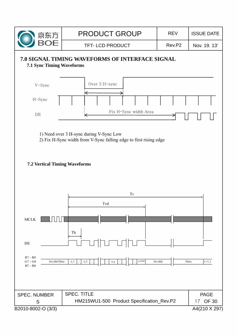
7.0 SIGNAL TIMING WAVEFORMS OF INTERFACE SIGNAL7 1 Sync Timing Waveforms7.1 Sync Timing Waveforms
V-Sync
H-Sync
Over 3 H-sync
DEFix H-Sync width Area
1) Need over 3 H-sync during V-Sync Low 2) Fix H-Sync width from V-Sync falling edge to first rising edge
7.2 Vertical Timing Waveforms
MCLK
Tv
Tvd
DE
x,1 x,2 x,y x+1,1x,1050Invalid Data DataInvalid
Th
R7 ~ R0G7 ~ G0B7 ~ B0
A4(210 X 297)
PAGE
OF 30SPEC. NUMBER
S
SPEC. TITLE
HM215WU1-500 Product Specification_Rev.P2
B2010-8002-O (3/3)
17
REV ISSUE DATEPRODUCT GROUP
Rev.P2TFT- LCD PRODUCT Nov. 19. 13’
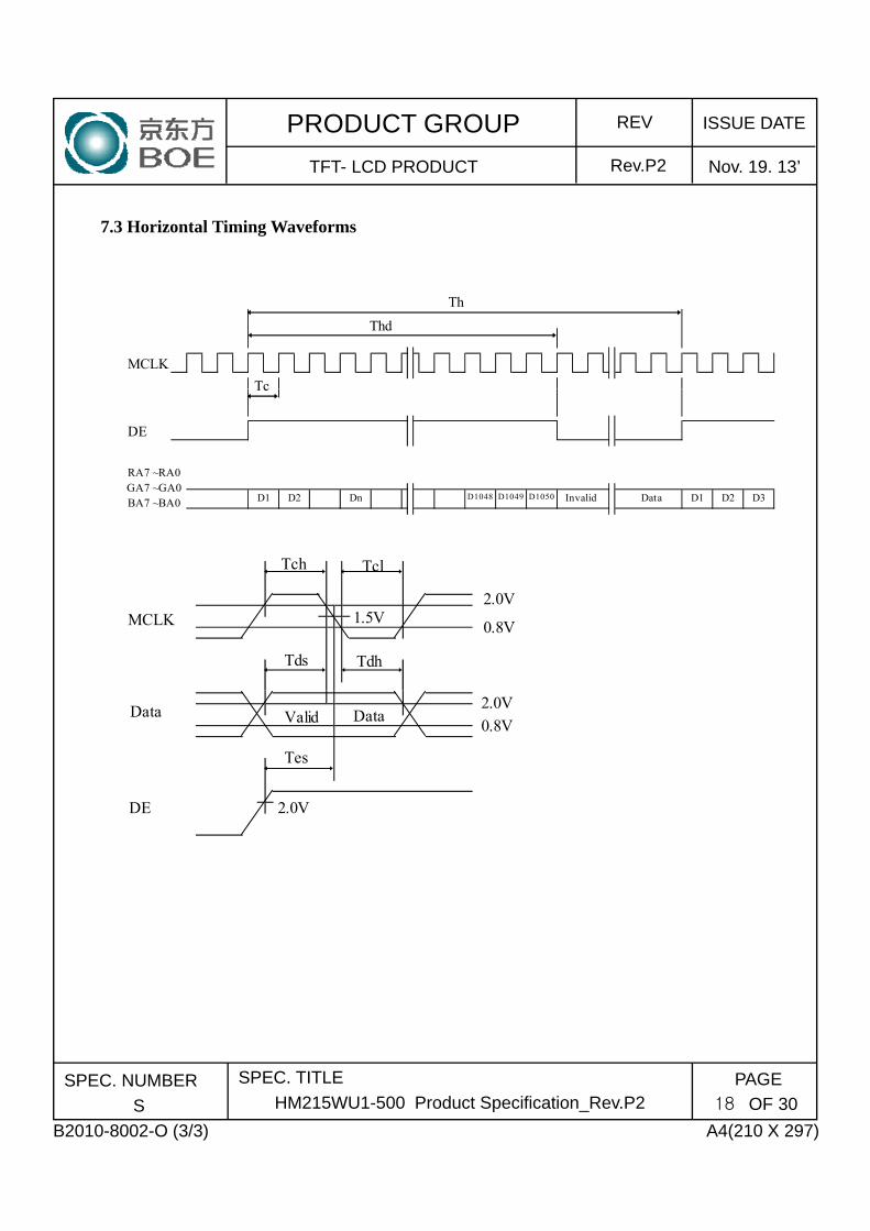
7.3 Horizontal Timing Waveforms
MCLK
Th
Thd
Tc
DE
D1 D2 Dn Data D1 D2 D3
InvalidD1048 D1049 D1050
Tc
RA7 ~RA0GA7 ~GA0BA7 ~BA0
Tch Tcl
TdhTds
2.0V
0.8VMCLK 1.5V
2.0V
0.8V
Tes
2.0V
Valid DataData
DE
A4(210 X 297)
PAGE
OF 30SPEC. NUMBER
S
SPEC. TITLE
HM215WU1-500 Product Specification_Rev.P2
B2010-8002-O (3/3)
18
REV ISSUE DATEPRODUCT GROUP
Rev.P2TFT- LCD PRODUCT Nov. 19. 13’
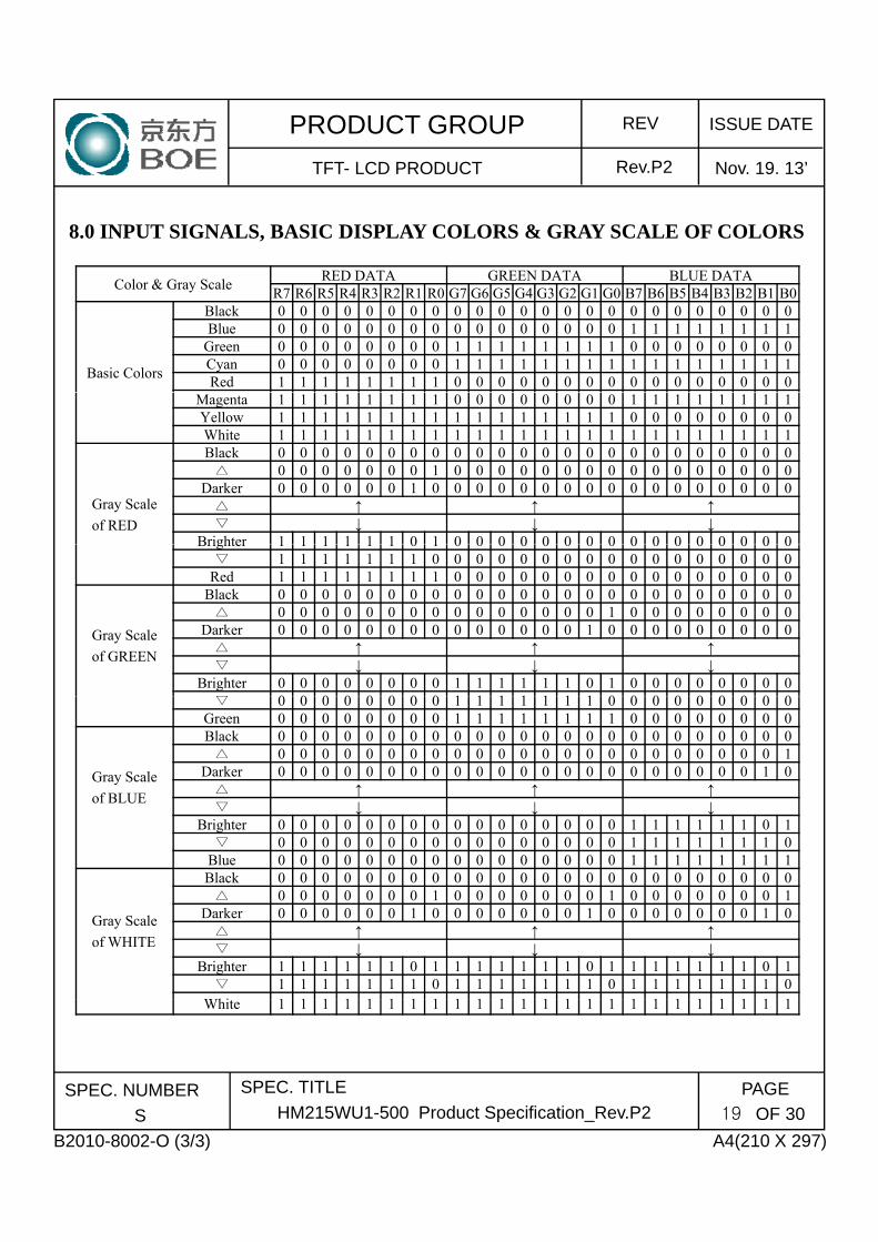
8.0 INPUT SIGNALS, BASIC DISPLAY COLORS & GRAY SCALE OF COLORS,
Color & Gray ScaleRED DATA GREEN DATA BLUE DATA
R7 R6 R5 R4 R3 R2 R1 R0 G7 G6 G5 G4 G3 G2 G1 G0 B7 B6 B5 B4 B3 B2 B1 B0
Basic Colors
Black 0 0 0 0 0 0 0 0 0 0 0 0 0 0 0 0 0 0 0 0 0 0 0 0Blue 0 0 0 0 0 0 0 0 0 0 0 0 0 0 0 0 1 1 1 1 1 1 1 1
Green 0 0 0 0 0 0 0 0 1 1 1 1 1 1 1 1 0 0 0 0 0 0 0 0Cyan 0 0 0 0 0 0 0 0 1 1 1 1 1 1 1 1 1 1 1 1 1 1 1 1Red 1 1 1 1 1 1 1 1 0 0 0 0 0 0 0 0 0 0 0 0 0 0 0 0
Magenta 1 1 1 1 1 1 1 1 0 0 0 0 0 0 0 0 1 1 1 1 1 1 1 1Yellow 1 1 1 1 1 1 1 1 1 1 1 1 1 1 1 1 0 0 0 0 0 0 0 0White 1 1 1 1 1 1 1 1 1 1 1 1 1 1 1 1 1 1 1 1 1 1 1 1
Gray Scale
of RED
Black 0 0 0 0 0 0 0 0 0 0 0 0 0 0 0 0 0 0 0 0 0 0 0 0 0 0 0 0 0 0 0 1 0 0 0 0 0 0 0 0 0 0 0 0 0 0 0 0
Darker 0 0 0 0 0 0 1 0 0 0 0 0 0 0 0 0 0 0 0 0 0 0 0 0 ↑ ↑ ↑ ↓ ↓ ↓
Brighter 1 1 1 1 1 1 0 1 0 0 0 0 0 0 0 0 0 0 0 0 0 0 0 0Brighter 1 1 1 1 1 1 0 1 0 0 0 0 0 0 0 0 0 0 0 0 0 0 0 0 1 1 1 1 1 1 1 0 0 0 0 0 0 0 0 0 0 0 0 0 0 0 0 0
Red 1 1 1 1 1 1 1 1 0 0 0 0 0 0 0 0 0 0 0 0 0 0 0 0
Gray Scale
of GREEN
Black 0 0 0 0 0 0 0 0 0 0 0 0 0 0 0 0 0 0 0 0 0 0 0 0 0 0 0 0 0 0 0 0 0 0 0 0 0 0 0 1 0 0 0 0 0 0 0 0
Darker 0 0 0 0 0 0 0 0 0 0 0 0 0 0 1 0 0 0 0 0 0 0 0 0 ↑ ↑ ↑ ↓ ↓ ↓
Brighter 0 0 0 0 0 0 0 0 1 1 1 1 1 1 0 1 0 0 0 0 0 0 0 0 0 0 0 0 0 0 0 0 1 1 1 1 1 1 1 0 0 0 0 0 0 0 0 0 0 0 0 0 0 0 0 0 1 1 1 1 1 1 1 0 0 0 0 0 0 0 0 0
Green 0 0 0 0 0 0 0 0 1 1 1 1 1 1 1 1 0 0 0 0 0 0 0 0
Gray Scale
of BLUE
Black 0 0 0 0 0 0 0 0 0 0 0 0 0 0 0 0 0 0 0 0 0 0 0 0 0 0 0 0 0 0 0 0 0 0 0 0 0 0 0 0 0 0 0 0 0 0 0 1
Darker 0 0 0 0 0 0 0 0 0 0 0 0 0 0 0 0 0 0 0 0 0 0 1 0 ↑ ↑ ↑ ↓ ↓ ↓
Brighter 0 0 0 0 0 0 0 0 0 0 0 0 0 0 0 0 1 1 1 1 1 1 0 1 0 0 0 0 0 0 0 0 0 0 0 0 0 0 0 0 1 1 1 1 1 1 1 0
Blue 0 0 0 0 0 0 0 0 0 0 0 0 0 0 0 0 1 1 1 1 1 1 1 1
Gray Scale
of WHITE
Black 0 0 0 0 0 0 0 0 0 0 0 0 0 0 0 0 0 0 0 0 0 0 0 0 0 0 0 0 0 0 0 1 0 0 0 0 0 0 0 1 0 0 0 0 0 0 0 1
Darker 0 0 0 0 0 0 1 0 0 0 0 0 0 0 1 0 0 0 0 0 0 0 1 0 ↑ ↑ ↑ ↓ ↓ ↓
Brighter 1 1 1 1 1 1 0 1 1 1 1 1 1 1 0 1 1 1 1 1 1 1 0 1 1 1 1 1 1 1 1 0 1 1 1 1 1 1 1 0 1 1 1 1 1 1 1 0
Whi 1 1 1 1 1 1 1 1 1 1 1 1 1 1 1 1 1 1 1 1 1 1 1 1
A4(210 X 297)
PAGE
OF 30SPEC. NUMBER
S
SPEC. TITLE
HM215WU1-500 Product Specification_Rev.P2
B2010-8002-O (3/3)
19
White 1 1 1 1 1 1 1 1 1 1 1 1 1 1 1 1 1 1 1 1 1 1 1 1
REV ISSUE DATEPRODUCT GROUP
Rev.P2TFT- LCD PRODUCT Nov. 19. 13’
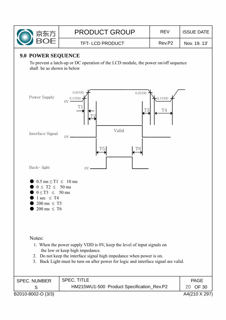
9.0 POWER SEQUENCET t l t h DC ti f th LCD d l th / ffTo prevent a latch-up or DC operation of the LCD module, the power on/off sequence shall be as shown in below
Power Supply
0.9VDD
0.1VDD
0.9VDD
0.1VDD0V
T1
Interface SignalValid
T2
T3
0V
0V
T4
Back- light
T5 T6
0V
0.5 ms ≤ T1 10 ms 0 T2 50 ms 0 ≤ T3 50 ms 1 sec T4 200 ms T5 200 ms T6
Notes:1. When the power supply VDD is 0V, keep the level of input signals on
the low or keep high impedance.2. Do not keep the interface signal high impedance when power is on.
A4(210 X 297)
PAGE
OF 30SPEC. NUMBER
S
SPEC. TITLE
HM215WU1-500 Product Specification_Rev.P2
B2010-8002-O (3/3)
20
p g g p p3. Back Light must be turn on after power for logic and interface signal are valid.
REV ISSUE DATEPRODUCT GROUP
Rev.P2TFT- LCD PRODUCT Nov. 19. 13’
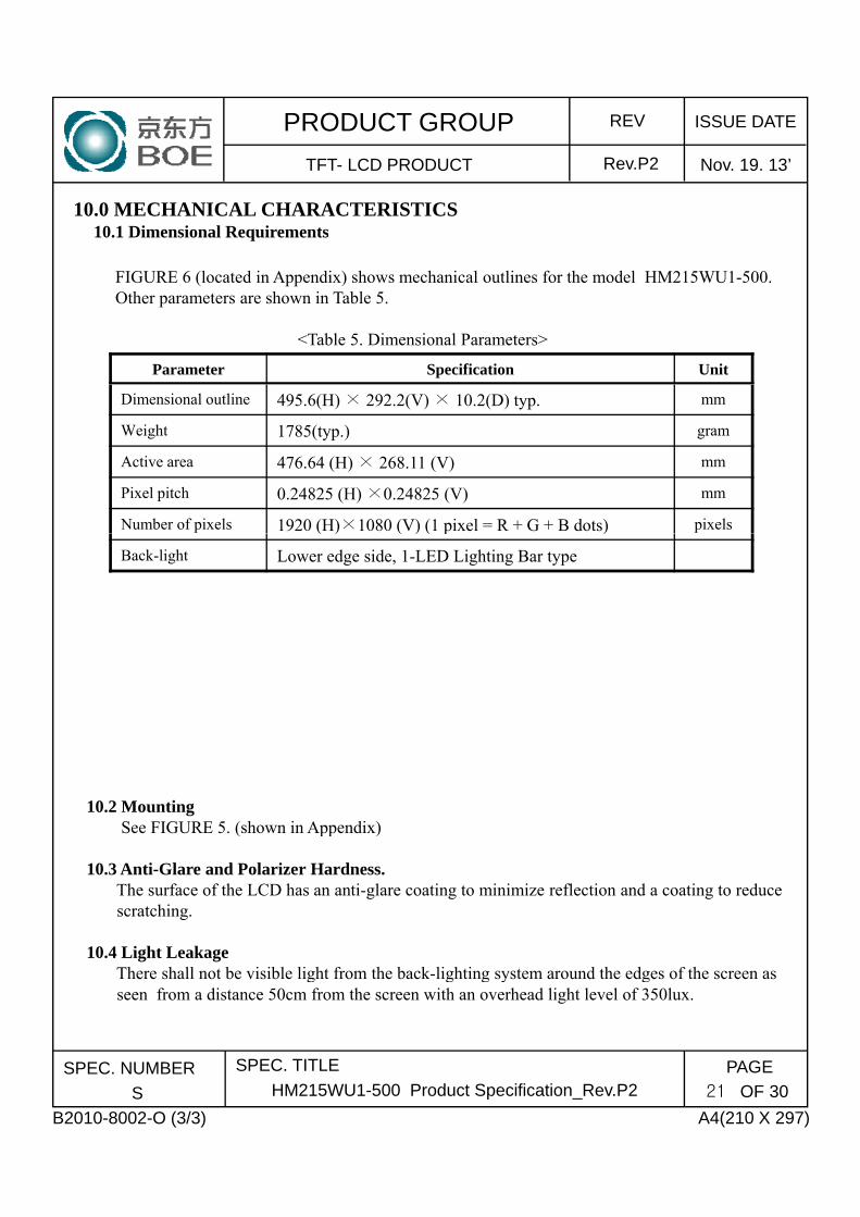
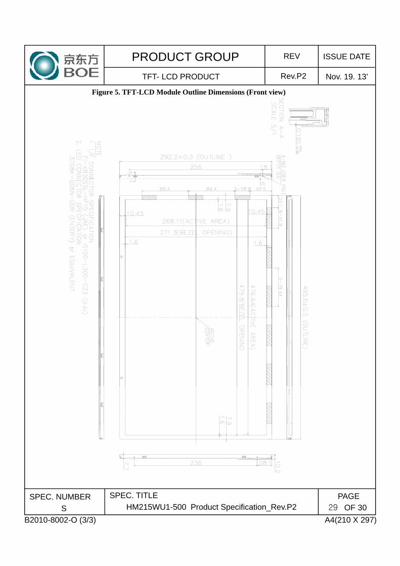
10.0 MECHANICAL CHARACTERISTICS10.1 Dimensional Requirements10.1 Dimensional Requirements
FIGURE 6 (located in Appendix) shows mechanical outlines for the model HM215WU1-500. Other parameters are shown in Table 5.
<Table 5. Dimensional Parameters>
Parameter Specification Unit
Dimensional outline 495.6(H) × 292.2(V) × 10.2(D) typ. mm
Weight 1785(typ.) gram
Active area 476.64 (H) × 268.11 (V) mm
Pixel pitch 0.24825 (H) ×0.24825 (V) mm
Number of pixels 1920 (H)×1080 (V) (1 pixel = R + G + B dots) pixels( ) ( ) ( p )
Back-light Lower edge side, 1-LED Lighting Bar type
10.2 Mounting See FIGURE 5 (shown in Appendix)See FIGURE 5. (shown in Appendix)
10.3 Anti-Glare and Polarizer Hardness.The surface of the LCD has an anti-glare coating to minimize reflection and a coating to reduce scratching.
10.4 Light LeakageThere shall not be visible light from the back-lighting system around the edges of the screen as
A4(210 X 297)
PAGE
OF 30SPEC. NUMBER
S
SPEC. TITLE
HM215WU1-500 Product Specification_Rev.P2
B2010-8002-O (3/3)
21
g g g y gseen from a distance 50cm from the screen with an overhead light level of 350lux.
REV ISSUE DATEPRODUCT GROUP
Rev.P2TFT- LCD PRODUCT Nov. 19. 13’
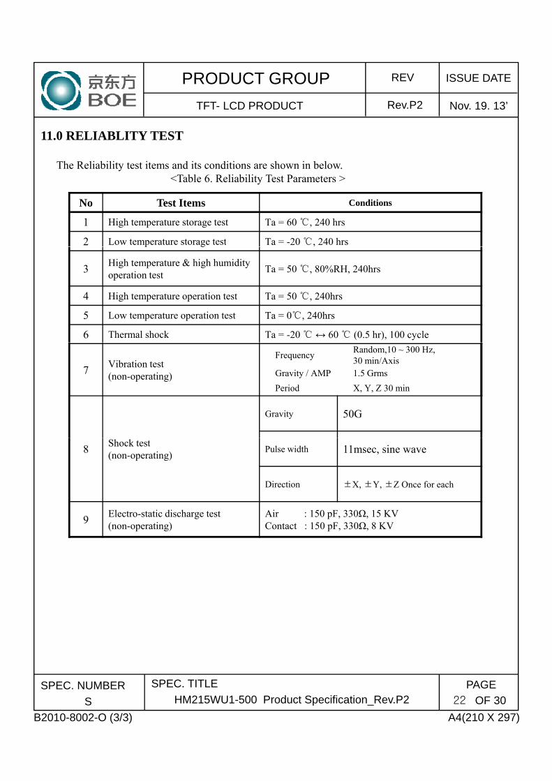
11.0 RELIABLITY TEST
The Reliability test items and its conditions are shown in below.<Table 6. Reliability Test Parameters >
No Test Items Conditions
1 High temperature storage test Ta = 60 , 240 hrs
2 Low temperature storage test Ta = -20 , 240 hrsp g
3High temperature & high humidity operation test
Ta = 50 , 80%RH, 240hrs
4 High temperature operation test Ta = 50 , 240hrs
5 Low temperature operation test Ta = 0, 240hrs
6 Thermal shock Ta = -20 ↔ 60 (0.5 hr), 100 cycle
7Vibration test(non-operating)
FrequencyRandom,10 ~ 300 Hz, 30 min/Axis
Gravity / AMP 1.5 Grms
Period X, Y, Z 30 min
Gravity 50G
8Shock test(non-operating)
Pulse width 11msec, sine wave
Direction ±X, ±Y, ±Z Once for each
9Electro-static discharge test (non-operating)
Air : 150 pF, 330Ω, 15 KV Contact : 150 pF, 330Ω, 8 KV
A4(210 X 297)
PAGE
OF 30SPEC. NUMBER
S
SPEC. TITLE
HM215WU1-500 Product Specification_Rev.P2
B2010-8002-O (3/3)
22
REV ISSUE DATEPRODUCT GROUP
Rev.P2TFT- LCD PRODUCT Nov. 19. 13’
12 0 HANDLING & CAUTIONS12.0 HANDLING & CAUTIONS
(1) Cautions when taking out the module Pick the pouch only, when taking out module from a shipping package.
(2) Cautions for handling the moduleAs the electrostatic discharges may break the LCD module, handle the LCD
module with care. Peel a protection sheet off from the LCD panel surface as slowly as possible.As the LCD panel and back - light element are made from fragile glass material,
impulse and pressure to the LCD module should be avoided.As the surface of the polarizer is very soft and easily scratched, use a soft dry
cloth without chemicals for cleaning. Do not pull the interface connector in or out while the LCD module is operating. Put the module display side down on a flat horizontal plane. Handle connectors and cables with care.
( ) i f h i(3) Cautions for the operationWhen the module is operating, do not lose CLK, ENAB signals. If any one of
these signals is lost, the LCD panel would be damaged. Obey the supply voltage sequence. If wrong sequence is applied, the module
would be damaged.(4) Cautions for the atmosphere Dew drop atmosphere should be avoided.
D t t d/ t th LCD d l i hi h t t d/ Do not store and/or operate the LCD module in a high temperature and/or humidity atmosphere. Storage in an electro-conductive polymer packing pouch and under relatively low temperature atmosphere is recommended.
(5) Cautions for the module characteristics Do not apply fixed pattern data signal to the LCD module at product aging. Applying fixed pattern for a long time may cause image sticking.
(6) Other cautions Do not disassemble and/or re assemble LCD module Do not disassemble and/or re-assemble LCD module. Do not re-adjust variable resistor or switch etc.When returning the module for repair or etc., Please pack the module not to be
broken. We recommend to use the original shipping packages.
A4(210 X 297)
PAGE
OF 30SPEC. NUMBER
S
SPEC. TITLE
HM215WU1-500 Product Specification_Rev.P2
B2010-8002-O (3/3)
23
REV ISSUE DATEPRODUCT GROUP
Rev.P2TFT- LCD PRODUCT Nov. 19. 13’
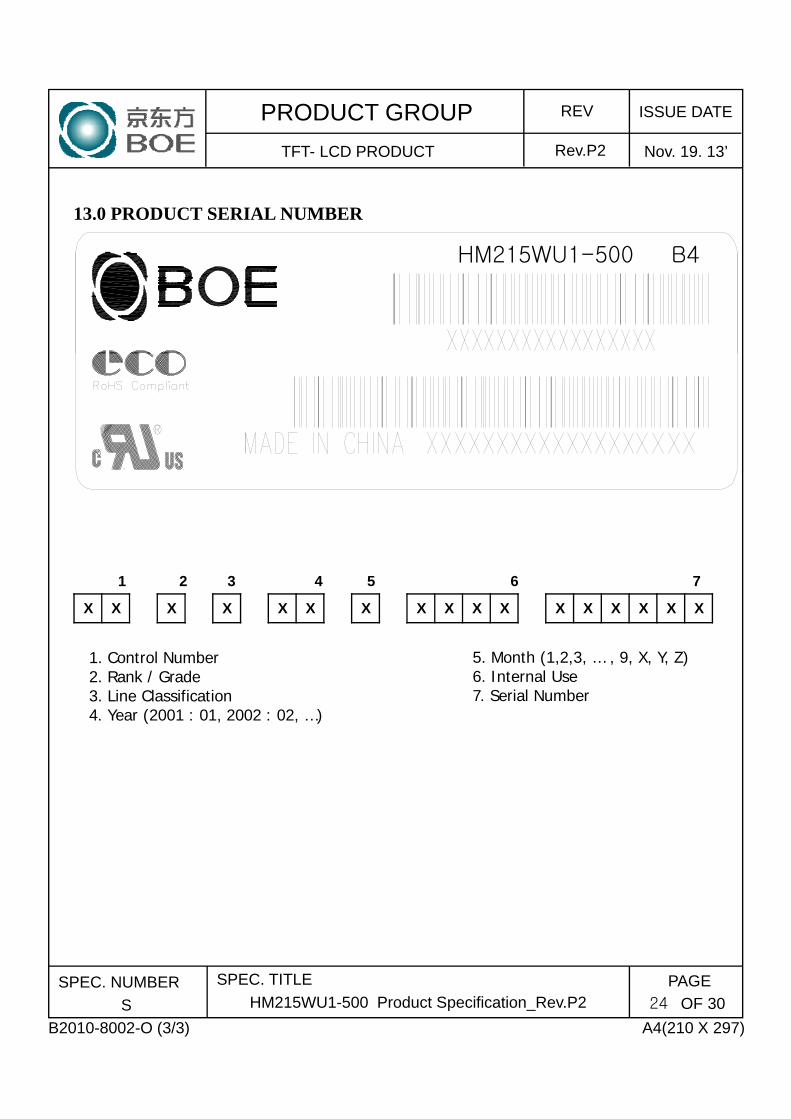
13 0 PRODUCT SERIAL NUMBER13.0 PRODUCT SERIAL NUMBER
HM215WU1-500 B4
1 2 3 4 5 6 7
X X X X X X X X X X X X X X X X X
1. Control Number2. Rank / Grade3. Line Classification 4. Year (2001 : 01, 2002 : 02, …)
5. Month (1,2,3, … , 9, X, Y, Z)6. Internal Use7. Serial Number
A4(210 X 297)
PAGE
OF 30SPEC. NUMBER
S
SPEC. TITLE
HM215WU1-500 Product Specification_Rev.P2
B2010-8002-O (3/3)
24
REV ISSUE DATEPRODUCT GROUP
Rev.P2TFT- LCD PRODUCT Nov. 19. 13’
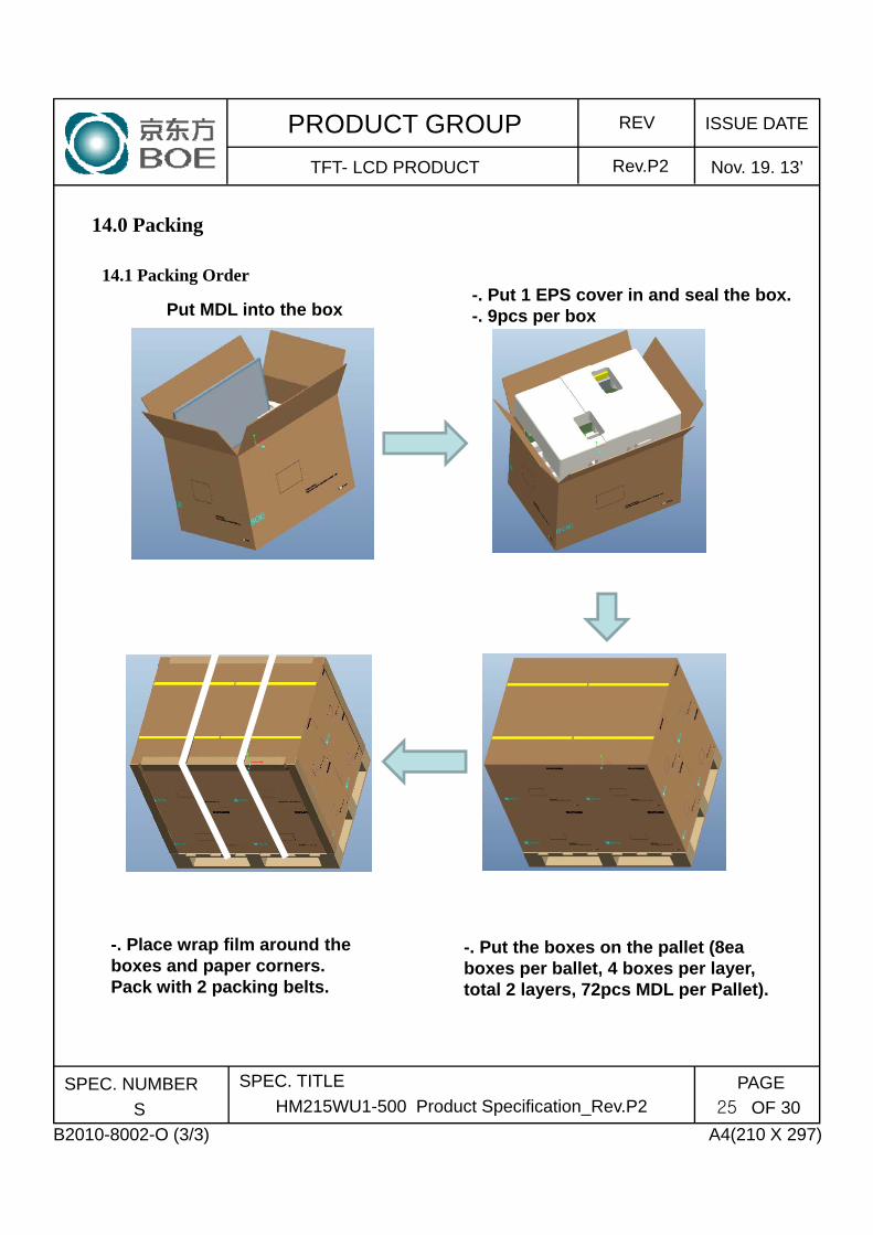
14.0 Packing
14.1 Packing Order
Put MDL into the box-. Put 1 EPS cover in and seal the box.-. 9pcs per box
-. Put the boxes on the pallet (8ea boxes per ballet, 4 boxes per layer, total 2 layers, 72pcs MDL per Pallet).
-. Place wrap film around the boxes and paper corners.Pack with 2 packing belts.
A4(210 X 297)
PAGE
OF 30SPEC. NUMBER
S
SPEC. TITLE
HM215WU1-500 Product Specification_Rev.P2
B2010-8002-O (3/3)
25
total 2 layers, 72pcs MDL per Pallet).p g
REV ISSUE DATEPRODUCT GROUP
Rev.P2TFT- LCD PRODUCT Nov. 19. 13’
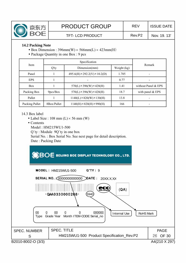
14.2 Packing Note Box Dimension : 396mm(W) 566mm(L) 423mm(H)Box Dimension : 396mm(W) 566mm(L) 423mm(H) Package Quantity in one Box : 9 pcs
ItemSpecification
RemarkQ'ty Dimension(mm) Weight (kg)
Panel 1 495.6(H)×292.2(V)×10.2(D) 1.785 -
EPS 1 - 0.77 -
Box 1 570(L)×396(W)×428(H) 1.41 without Panel & EPS
Packing Box 9pcs/Box 570(L)×396(W)×428(H) 18.7 with panel & EPS
Pallet 1 1140(L)×820(W)×130(H) 13.8 -
Packing Pallet 8Box/Pallet 1140(H)×820(H)×990(H) 166 -
14.3 Box label Label Size : 108 mm (L) 56 mm (W) Contents
Model : HM215WU1-500Q`ty : Module 9Q`ty in one boxSerial No. : Box Serial No. See next page for detail description.Date : Packing Date
0000000000000 20XX.X.XX
9HM215WU1-500
0000000000000 20XX.X.XX
00 0 00 0 0 000000
5940
A4(210 X 297)
PAGE
OF 30SPEC. NUMBER
S
SPEC. TITLE
HM215WU1-500 Product Specification_Rev.P2
B2010-8002-O (3/3)
26
00 0 00 0 0 000000Type Grade Year Month ITEM-CODE Serial_no
Internal Use RoHS Mark
REV ISSUE DATEPRODUCT GROUP
Rev.P2TFT- LCD PRODUCT Nov. 19. 13’
15.0 APPENDIX
Figure 1. Measurement Set Up
(L = 5 0 c m )
Figure 2. White Luminance and Uniformity Measurement Locations (9 points)
1) 1
192 810 1728
1081) 2 1) 3
540
972
1) 4 1) 5
1) 7 1) 8 1) 9
1) 6
A4(210 X 297)
PAGE
OF 30SPEC. NUMBER
S
SPEC. TITLE
HM215WU1-500 Product Specification_Rev.P2
B2010-8002-O (3/3)
27
REV ISSUE DATEPRODUCT GROUP
Rev.P2TFT- LCD PRODUCT Nov. 19. 13’
Figure 3. Response Time Testing
Display data
OpticalResponse
Black(TFT ON)White(TFT OFF)
100%90%
10%
TR TF
White(TFT OFF)
10%0%
Time
Figure 4. Cross Modulation Test Description
YB(7D/8,W/2)
(3D/4, 3W/4)
L31
(D/4, W/4)
VIEW AREA VIEW AREA
YB - YA
YA
Cross-Talk (%) = × 100
YA (7D/8,W/2)L0
(D, W) (D, W)
Where: YA = Initial luminance of measured area (cd/m2)YB = Subsequent luminance of measured area (cd/m2)
The location measured will be exactly the same in both patterns
A4(210 X 297)
PAGE
OF 30SPEC. NUMBER
S
SPEC. TITLE
HM215WU1-500 Product Specification_Rev.P2
B2010-8002-O (3/3)
28
REV ISSUE DATEPRODUCT GROUP
Rev.P2TFT- LCD PRODUCT Nov. 19. 13’
Figure 5. TFT-LCD Module Outline Dimensions (Front view)
A4(210 X 297)
PAGE
OF 30SPEC. NUMBER
S
SPEC. TITLE
HM215WU1-500 Product Specification_Rev.P2
B2010-8002-O (3/3)
29
REV ISSUE DATEPRODUCT GROUP
Rev.P2TFT- LCD PRODUCT Nov. 19. 13’
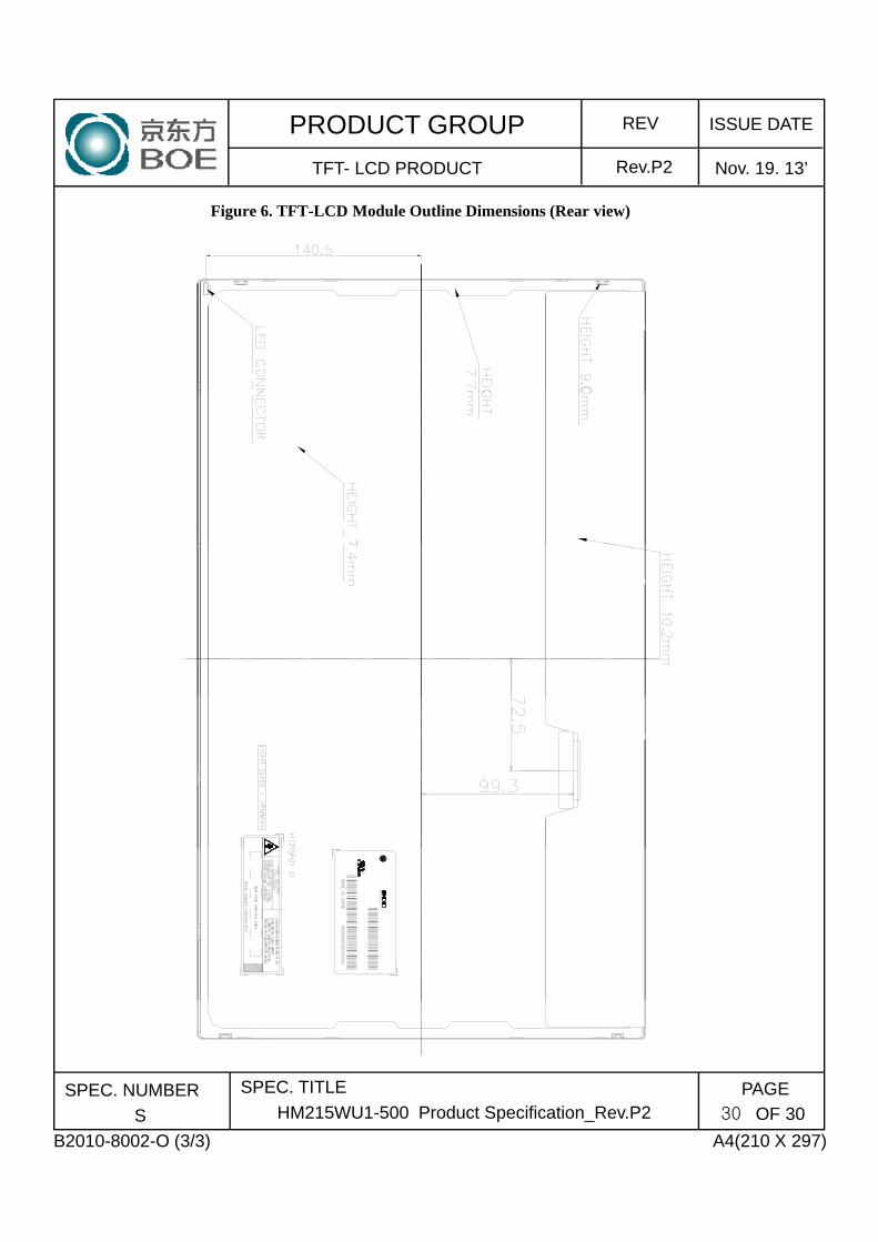
Figure 6. TFT-LCD Module Outline Dimensions (Rear view)
A4(210 X 297)
PAGE
OF 30SPEC. NUMBER
S
SPEC. TITLE
HM215WU1-500 Product Specification_Rev.P2
B2010-8002-O (3/3)
30


![Investor Presentation (3Q13 Results).pptx [Read-Only]bh.listedcompany.com/misc/PRESN/20131119-BH-investorPRESN.pdf · PG.2 Disclaimer • The information contained in this presentation](https://img.pdfslide.us/doc/110x75/5f06ce197e708231d419d2a8/investor-presentation-3q13-resultspptx-read-onlybh-pg2-disclaimer-a-the.jpg)

![Ver. Date Page Descriptionultran.ru/sites/default/files/catalog/svetodiody/brend/datasheets/com... · Object substance Maximum content [ppm] Cadmium and its compound 100 Hexavalent](https://img.pdfslide.us/doc/110x75/5f0f42c27e708231d44347f7/ver-date-page-object-substance-maximum-content-ppm-cadmium-and-its-compound-100.jpg)