Embed Size (px)
Citation preview

Highly Miniaturized Antennas and Filters for
Wireless Applications
by
Reza Azadegan
A dissertation submitted in partial fulfillmentof the requirements for the degree of
Doctor of Philosophy(Electrical Engineering)
in The University of Michigan2004
Doctoral Committee:Professor Kamal Sarabandi, ChairAssistant Professor Michael P. FlynnProfessor John W. HalloranProfessor Gabriel M. RebeizProfessor John L. Volakis

c© Reza Azadegan 2004All Rights Reserved

ABSTRACT
Highly Miniaturized Antennas and Filters for Wireless Applications
by
Reza Azadegan
Chair: Kamal Sarabandi
A novel approach to miniaturize antennas and microwave filters for wireless sys-
tems is presented. This approach is based on a proper choice of a miniature topology,
which at the same time offers minimal loss. The proposed topology has been used
to design a miniaturized slot antenna structure whose dimensions are as small as
0.05λ0 × 0.05λ0 with a gain of −3 dBi. A number of similar miniaturized topologies,
including a miniaturized folded-slot, its complementary and self-complementary pairs
have also been designed to provide miniaturized antennas with enhanced bandwidths.
Based on the same premise, miniaturization of direct-coupled and cross-coupled
filters are demonstrated. Although miniaturization is expected to adversely affect
the Q of a filter, the proposed filters exhibit a comparable Q to that of standard size
microstrip filters due to the inherent higher Q of a slot-line.
Finally, a high-impedance miniaturized antenna is proposed, followed by a radar
cross-section (RCS) measurement technique to extract its input impedance. Such a
high-impedance antenna may be a suitable candidate for emerging high-impedance
low-power micro- and nano-devices used in future wireless systems.

To my mother Batool (Akhtar), my father Jahangir,
my wife Zeinab, and my son Mohammad-Hosein
ii

ACKNOWLEDGEMENTS
I would first like to thank my advisor, Professor Kamal Sarabandi for his strong
support and encouragement. I should commend him for two things in particular.
First is the enormous amount of time he spends with his students providing them
with advice and thoughtful comments. Second is his exemplary courage to embark
on novel research avenues.
I also thank my dissertation committee, Prof. Michael P. Flynn, Prof. John
Halloran, Prof. Gabriel M. Rebeiz, and Prof. John L. Volakis. for their support and
feedback. I should acknowledge Prof. Volakis for his input on the different aspects of
the numerical simulation of antennas.
Special thanks are due to Prof. Liepa, Prof. Senior, and Prof. Tai for numerous
technical conversations that we have had regarding different topics in electromagnet-
ics. On a personal level, Dr. Liepa has been a very kind friend to me as well as an
outstanding expert on electromagnetic measurements.
I would like to acknowledge breadth and depth of help I have received from my
friends at the Radiation Laboratory of The University of Michigan. The spirit of
perseverance and cooperation in the RADLAB produces a unique environment that
nurtures academic excellence.
This acknowledgment would be incomplete without referring to my Iranian friends
at The University of Michigan whose presence made my stay in Ann Arbor a more
pleasant experience. Special thanks to my very good friend Mr. Alireza Tabatabaeene-
jad with whom I had long conversations on a variety of issues, and to many others.
iii

Mrs. Susan Charnley and Mr. Masoud Agah deserve a special mention. Dr.
Charnley has kindly helped me in editing a considerable portion of this manuscript
for style while it was developing. Masoud was kind enough to read my dissertation
in its entirety and provide helpful suggestions.
Finally, I would like to express my sincere gratitude to my family whose emotional
support has been essential in fulfilling this endeavor; to my mother for being my
inspiration; to my father for his rationality; to my wife for her continued love and
patience, and to my son for being so sweet.
iv

TABLE OF CONTENTS
DEDICATION . . . . . . . . . . . . . . . . . . . . . . . . . . . . . . . . . . ii
ACKNOWLEDGEMENTS . . . . . . . . . . . . . . . . . . . . . . . . . . iii
LIST OF TABLES . . . . . . . . . . . . . . . . . . . . . . . . . . . . . . . . viii
LIST OF FIGURES . . . . . . . . . . . . . . . . . . . . . . . . . . . . . . . ix
CHAPTER
1 Introduction . . . . . . . . . . . . . . . . . . . . . . . . . . . . . . . 11.1 Motivation and Background . . . . . . . . . . . . . . . . . . 11.2 Thesis Overview . . . . . . . . . . . . . . . . . . . . . . . . . 8
2 A Compact Quarter-wavelength Slot Antenna Topology . . . . . . . 122.1 Introduction . . . . . . . . . . . . . . . . . . . . . . . . . . . 122.2 Compact Spiral Antennas . . . . . . . . . . . . . . . . . . . . 142.3 A Miniature Quarter-wave Topology . . . . . . . . . . . . . . 162.4 Realization and Measurements . . . . . . . . . . . . . . . . . 222.5 Conclusion . . . . . . . . . . . . . . . . . . . . . . . . . . . . 29
3 Miniaturization of Slot Antennas . . . . . . . . . . . . . . . . . . . . 303.1 Introduction . . . . . . . . . . . . . . . . . . . . . . . . . . . 30
3.1.1 Background . . . . . . . . . . . . . . . . . . . . . . . 303.1.2 Fundamental Limitations of Small Antennas . . . . . 313.1.3 Approaches for Antenna Miniaturization . . . . . . . 31
3.2 Miniaturized Antenna Geometry . . . . . . . . . . . . . . . . 343.2.1 Slot Radiator Topology . . . . . . . . . . . . . . . . . 343.2.2 Antenna Feed . . . . . . . . . . . . . . . . . . . . . . 37
3.3 Design Procedure . . . . . . . . . . . . . . . . . . . . . . . . 383.4 Full-Wave Simulation and Tuning . . . . . . . . . . . . . . . 40
3.4.1 Equivalent-Circuit Model . . . . . . . . . . . . . . . . 433.4.2 Antenna Matching . . . . . . . . . . . . . . . . . . . . 45
3.5 Antenna Simulation and Measurements . . . . . . . . . . . . 483.6 Conformability to Curved Platforms . . . . . . . . . . . . . . 54
v

3.7 Conclusion . . . . . . . . . . . . . . . . . . . . . . . . . . . . 60
4 Bandwidth Enhancement of Miniaturized Slot Antennas Using Folded,Complementary and Self-Complementary Realizations . . . . . . . . 61
4.1 Introduction . . . . . . . . . . . . . . . . . . . . . . . . . . . 614.2 Miniaturized Folded Slot Antenna . . . . . . . . . . . . . . . 644.3 Miniaturized Folded Printed Wire Antenna . . . . . . . . . . 714.4 Miniaturized Self-Complementary Folded Antenna . . . . . . 77
4.4.1 Impedance Matching . . . . . . . . . . . . . . . . . . 784.5 Self-Complimentary H-Shaped Antenna . . . . . . . . . . . . 844.6 Conclusion . . . . . . . . . . . . . . . . . . . . . . . . . . . . 92
5 RF Filter Miniaturization Using a High-Q Slot-line Resonator . . . . 945.1 Introduction . . . . . . . . . . . . . . . . . . . . . . . . . . . 945.2 Miniaturized Slot-line Resonator Topology . . . . . . . . . . 975.3 Direct-Coupled 4-Pole Filter . . . . . . . . . . . . . . . . . . 104
5.3.1 Coupling Structures . . . . . . . . . . . . . . . . . . . 1045.3.2 External Coupling . . . . . . . . . . . . . . . . . . . . 1095.3.3 Examples . . . . . . . . . . . . . . . . . . . . . . . . . 110
5.4 Cross Coupled Miniature Filters . . . . . . . . . . . . . . . . 1135.5 Conclusions . . . . . . . . . . . . . . . . . . . . . . . . . . . 123
6 RCS Measurement Technique to Extract the Input Impedance of High-Impedance Miniaturized Slot Antennas . . . . . . . . . . . . . . . . 125
6.1 Introduction . . . . . . . . . . . . . . . . . . . . . . . . . . . 1256.2 Methodology . . . . . . . . . . . . . . . . . . . . . . . . . . . 1276.3 Formulation . . . . . . . . . . . . . . . . . . . . . . . . . . . 129
6.3.1 Scattering from an Electric-Dipole Antenna . . . . . . 1296.3.2 Scattering from a Magnetic Dipole Antenna . . . . . . 1326.3.3 Radar Cross-Section of an Aperture Antenna . . . . . 133
6.4 Analytical Results . . . . . . . . . . . . . . . . . . . . . . . . 1366.5 Numerical Simulation . . . . . . . . . . . . . . . . . . . . . . 137
6.5.1 Center-fed Slot Antenna . . . . . . . . . . . . . . . . 1386.5.2 High-impedance Miniaturized Slot Antenna . . . . . . 141
6.6 Measurement of High-Impedance Antenna . . . . . . . . . . . 1456.7 Conclusion . . . . . . . . . . . . . . . . . . . . . . . . . . . . 147
7 Conclusions and Recommendations for Future Work . . . . . . . . . 1497.1 Summary . . . . . . . . . . . . . . . . . . . . . . . . . . . . . 1497.2 Contributions . . . . . . . . . . . . . . . . . . . . . . . . . . 150
7.2.1 Antenna Miniaturization . . . . . . . . . . . . . . . . 1507.2.2 Bandwidth Enhancement of Miniaturized Antennas . 1507.2.3 Microwave Filter Miniaturization . . . . . . . . . . . . 1517.2.4 High-Impedance Antenna Measurement . . . . . . . . 151
7.3 Future Work . . . . . . . . . . . . . . . . . . . . . . . . . . . 152
vi

APPENDIX . . . . . . . . . . . . . . . . . . . . . . . . . . . . . . . . . . . . 155
BIBLIOGRAPHY . . . . . . . . . . . . . . . . . . . . . . . . . . . . . . . . 169
vii

LIST OF TABLES
Table
2.1 Resonant frequencies, gains, and ground plane sizes of the three minia-turized slot antennas of Fig. 2.7. . . . . . . . . . . . . . . . . . . . . . 25
3.1 Slot-line characteristics for two different values of slot width w, andthe dielectric constant of εr = 2.2 and thickness of h = 0.787(mm) andf = 300 MHz. . . . . . . . . . . . . . . . . . . . . . . . . . . . . . . . 38
3.2 The parameters of the Genetic Algorithm optimizer. . . . . . . . . . . 45
3.3 The equivalent circuit parameters of the microstrip fed slot antenna. . 45
3.4 The physical length of the 50 Ω microstrip line needed for realizing thetermination susceptance, where the dielectric material properties areas specified in Table 3.1. . . . . . . . . . . . . . . . . . . . . . . . . . 47
3.5 Antenna characteristics as a function of two different size ground planescompared with the simulated results for the same antenna on an infiniteground plane. . . . . . . . . . . . . . . . . . . . . . . . . . . . . . . . 51
4.1 Comparison among characteristics of miniaturized slot, miniaturizedfolded slot, and miniaturized printed folded dipole antennas. . . . . . 76
5.1 The effect of the slot to strip width (s/w) on the unloaded Q of theminiaturized slot-line resonators. . . . . . . . . . . . . . . . . . . . . 100
viii
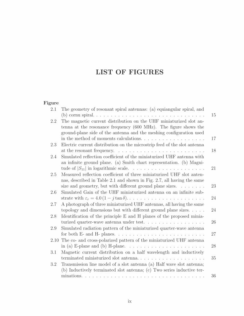
LIST OF FIGURES
Figure
2.1 The geometry of resonant spiral antennas: (a) equiangular spiral, and(b) cornu spiral. . . . . . . . . . . . . . . . . . . . . . . . . . . . . . . 15
2.2 The magnetic current distribution on the UHF miniaturized slot an-tenna at the resonance frequency (600 MHz). The figure shows theground-plane side of the antenna and the meshing configuration usedin the method of moments calculations. . . . . . . . . . . . . . . . . . 17
2.3 Electric current distribution on the microstrip feed of the slot antennaat the resonant frequency. . . . . . . . . . . . . . . . . . . . . . . . . 18
2.4 Simulated reflection coefficient of the miniaturized UHF antenna withan infinite ground plane. (a) Smith chart representation. (b) Magni-tude of |S11| in logarithmic scale. . . . . . . . . . . . . . . . . . . . . 21
2.5 Measured reflection coefficient of three miniaturized UHF slot anten-nas, described in Table 2.1 and shown in Fig. 2.7, all having the samesize and geometry, but with different ground plane sizes. . . . . . . . 23
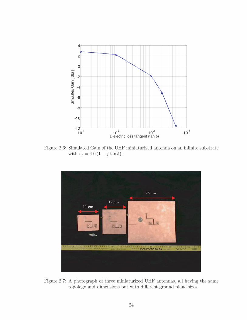
2.6 Simulated Gain of the UHF miniaturized antenna on an infinite sub-strate with εr = 4.0 (1 − j tan δ). . . . . . . . . . . . . . . . . . . . . . 24
2.7 A photograph of three miniaturized UHF antennas, all having the sametopology and dimensions but with different ground plane sizes. . . . . 24
2.8 Identification of the principle E and H planes of the proposed minia-turized quarter-wave antenna under test. . . . . . . . . . . . . . . . . 26
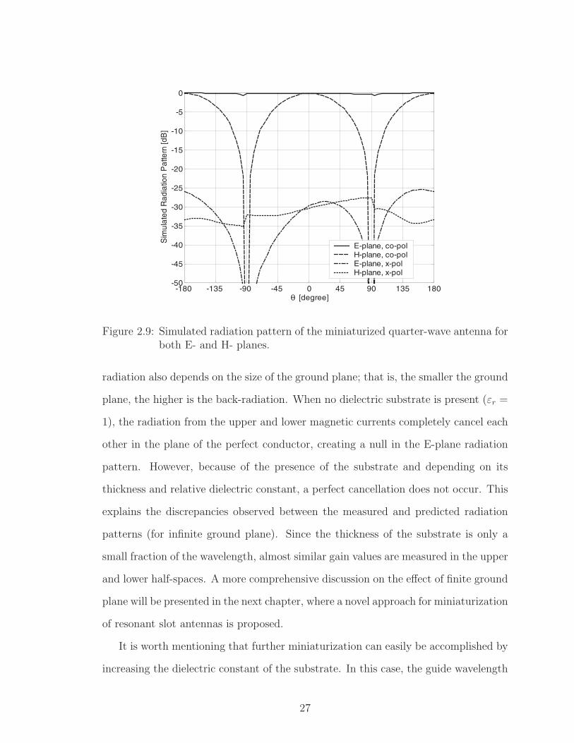
2.9 Simulated radiation pattern of the miniaturized quarter-wave antennafor both E- and H- planes. . . . . . . . . . . . . . . . . . . . . . . . . 27
2.10 The co- and cross-polarized pattern of the miniaturized UHF antennain (a) E-plane and (b) H-plane. . . . . . . . . . . . . . . . . . . . . . 28
3.1 Magnetic current distribution on a half wavelength and inductivelyterminated miniaturized slot antenna. . . . . . . . . . . . . . . . . . . 35
3.2 Transmission line model of a slot antenna (a) Half wave slot antenna;(b) Inductively terminated slot antenna; (c) Two series inductive ter-minations. . . . . . . . . . . . . . . . . . . . . . . . . . . . . . . . . . 36
ix
3.3 Proposed antenna geometry fed by a two-port microstrip feed. Thistwo-port geometry is used to find out the exact resonant frequency ofthe inductively loaded slot. . . . . . . . . . . . . . . . . . . . . . . . . 37
3.4 S-parameters of the two-port antenna shown in Fig. 3.3. . . . . . . . 41
3.5 Topology of the equivalent circuit for the two-port antenna. . . . . . 42
3.6 Y-parameters of the two-port antenna after deembedding the microstripfeed lines. . . . . . . . . . . . . . . . . . . . . . . . . . . . . . . . . . 44
3.7 Comparison between the full-wave simulated S-parameters of the an-tenna and that of the equivalent circuit. . . . . . . . . . . . . . . . . 46
3.8 The required terminating admittance for the second port of the two-port model in order to match the antenna to a 50 Ω line. . . . . . . . 46
3.9 The geometry of the antenna and its feed designed to operate at 300 MHz. 48
3.10 Measured and simulated return loss of the miniaturized antenna. . . . 49
3.11 A photograph of the fabricated miniaturized slot antenna at 300 MHz. 50
3.12 Simulated radiation pattern of the miniaturized antenna. . . . . . . . 52
3.13 Measured radiation patterns of the antenna with a small (0.2λ0×0.2λ0)and a larger (0.5λ0 × 0.5λ0) Ground Plane (GP): (a) H-plane pattern,(b) E-plane pattern. . . . . . . . . . . . . . . . . . . . . . . . . . . . 53
3.14 A photograph of the miniaturized slot antenna conformed into a curvedsurface along the H-plane. . . . . . . . . . . . . . . . . . . . . . . . . 55
3.15 Comparison between the measured radiation pattern of the conformedminiaturized slot antenna of Fig. 3.14 with that of its planar counter-part having a large ground plane (GP) with dimensions of (0.5λ0 ×0.5λ0): (a) H-plane pattern, (b) E-plane pattern. . . . . . . . . . . . . 57
3.16 A photograph of the miniaturized slot antenna conformed into a curvedsurface along the E-plane. . . . . . . . . . . . . . . . . . . . . . . . . 58
3.17 Comparison between the measured radiation pattern of the conformedminiaturized slot antenna of Fig. 3.16 with that of its planar counter-part having a large ground plane (GP) with dimensions of (0.5λ0 ×0.5λ0): (a) H-plane pattern, (b) E-plane pattern. . . . . . . . . . . . . 59
4.1 The layout and the the simulated input impedance of the miniaturizedslot antenna around its resonance. . . . . . . . . . . . . . . . . . . . . 64
4.2 The layout and the simulated input impedance of the miniaturizedfolded slot antenna around its resonance. . . . . . . . . . . . . . . . . 66
4.3 Miniaturized folded-slot antenna fed by a capacitively coupled CPWline. . . . . . . . . . . . . . . . . . . . . . . . . . . . . . . . . . . . . 67
4.4 Simulated and measured input return loss of the miniaturized foldedslot antenna of Fig. 4.3. . . . . . . . . . . . . . . . . . . . . . . . . . 68
4.5 Measured radiation pattern of the miniaturized folded slot antenna ofFig. 4.3. (a) H-plane pattern, (b) E-plane pattern. . . . . . . . . . . . 70
4.6 Layout of the miniaturized folded printed wire antenna, and the realand imaginary parts of its input admittance. . . . . . . . . . . . . . . 72
4.7 Merchand balun architecture. . . . . . . . . . . . . . . . . . . . . . . 73
x

4.8 The miniaturized folded printed wire antenna with balanced feed andfine tuning setup. . . . . . . . . . . . . . . . . . . . . . . . . . . . . . 74
4.9 Simulated and measured input return loss of the miniaturized antennain Fig. 4.8. . . . . . . . . . . . . . . . . . . . . . . . . . . . . . . . . . 74
4.10 E- and H-plane measured radiation patterns of the miniaturized foldedprinted wire of Fig. 4.8. . . . . . . . . . . . . . . . . . . . . . . . . . . 75
4.11 The simulated radiation pattern of the miniaturized folded printed wireantenna without a balun. . . . . . . . . . . . . . . . . . . . . . . . . . 75
4.12 The miniaturized self-complementary folded antenna fed by a two-portself-complementary asymmetric CPW-line. . . . . . . . . . . . . . . . 78
4.13 The two-port simulated S-parameters of the miniaturized self-complementaryfolded antenna of Fig. 4.12 to be used for obtaining a proper loss-lessmatching network. . . . . . . . . . . . . . . . . . . . . . . . . . . . . 79
4.14 The equivalent circuit of the required matching network to a 50 Ω line. 80
4.15 The geometry of the miniaturized self-complementary folded antennaalong with the distributed-element realization of the matching networkof Fig. 4.14. . . . . . . . . . . . . . . . . . . . . . . . . . . . . . . . . 80
4.16 The measured, simulated, input return losses of the antenna of Fig. 4.15,as well as that of the equivalent circuit model of Fig. 4.14. . . . . . . 81
4.17 Comparison between the measured and simulated radiation patterns ofthe miniaturized self-complementary antenna on three different planesof (a): φ = 0, (b): φ = 45, and (c): φ = 90. . . . . . . . . . . . . . 83
4.18 The topology of a self-complementary H-antenna fed by a short-circuitedmicrostrip line. . . . . . . . . . . . . . . . . . . . . . . . . . . . . . . 85
4.19 Measured and simulated return losses of the H-antenna in Fig. 4.18, aswell as that of the same structure without dielectric (εr = 1.0). . . . . 85
4.20 Comparison between the measured and simulated gains of the self-complementary H-antenna as a function of frequency. . . . . . . . . . 86
4.21 Comparison between the measured and simulated gain of the self-complementary H-antenna as a function of frequency. . . . . . . . . . 87
4.22 Comparison between the measured and simulated radiation patterns ofthe self-complementary H antenna at 1.5 GHz for three cuts of φ = 0,φ = 45, φ = 90; (a): measurements, (b): simulations. . . . . . . . . 88
4.23 Comparison between the measured and simulated radiation patterns ofthe self-complementary H antenna at 2.0 GHz for three cuts of φ = 0,φ = 45, φ = 90; (a): measurements, (b): simulations. . . . . . . . . 89
4.24 Comparison between the measured and simulated radiation patterns ofthe self-complementary H antenna at 2.5 GHz for three cuts of φ = 0,φ = 45, φ = 90; (a): measurements, (b): simulations. . . . . . . . . 90
4.25 Comparison between the measured and simulated radiation patterns ofthe self-complementary H antenna at 3.0 GHz for three cuts of φ = 0,φ = 45, φ = 90; (a): measurements, (b): simulations. . . . . . . . . 91
xi
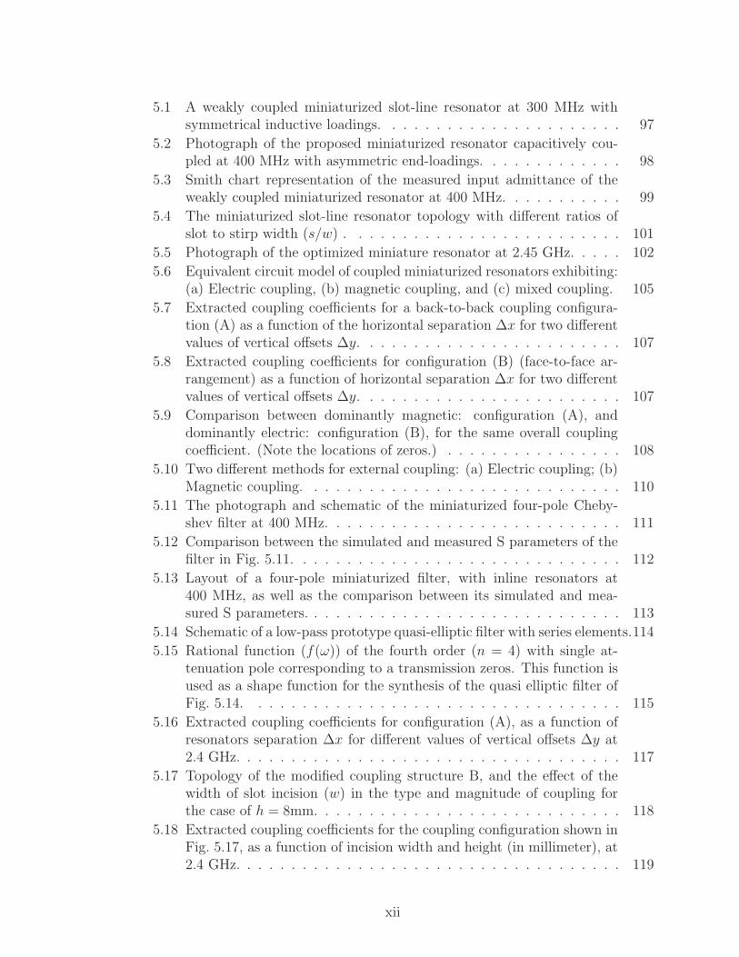
5.1 A weakly coupled miniaturized slot-line resonator at 300 MHz withsymmetrical inductive loadings. . . . . . . . . . . . . . . . . . . . . . 97
5.2 Photograph of the proposed miniaturized resonator capacitively cou-pled at 400 MHz with asymmetric end-loadings. . . . . . . . . . . . . 98
5.3 Smith chart representation of the measured input admittance of theweakly coupled miniaturized resonator at 400 MHz. . . . . . . . . . . 99
5.4 The miniaturized slot-line resonator topology with different ratios ofslot to stirp width (s/w) . . . . . . . . . . . . . . . . . . . . . . . . . 101
5.5 Photograph of the optimized miniature resonator at 2.45 GHz. . . . . 102
5.6 Equivalent circuit model of coupled miniaturized resonators exhibiting:(a) Electric coupling, (b) magnetic coupling, and (c) mixed coupling. 105
5.7 Extracted coupling coefficients for a back-to-back coupling configura-tion (A) as a function of the horizontal separation ∆x for two differentvalues of vertical offsets ∆y. . . . . . . . . . . . . . . . . . . . . . . . 107
5.8 Extracted coupling coefficients for configuration (B) (face-to-face ar-rangement) as a function of horizontal separation ∆x for two differentvalues of vertical offsets ∆y. . . . . . . . . . . . . . . . . . . . . . . . 107
5.9 Comparison between dominantly magnetic: configuration (A), anddominantly electric: configuration (B), for the same overall couplingcoefficient. (Note the locations of zeros.) . . . . . . . . . . . . . . . . 108
5.10 Two different methods for external coupling: (a) Electric coupling; (b)Magnetic coupling. . . . . . . . . . . . . . . . . . . . . . . . . . . . . 110
5.11 The photograph and schematic of the miniaturized four-pole Cheby-shev filter at 400 MHz. . . . . . . . . . . . . . . . . . . . . . . . . . . 111
5.12 Comparison between the simulated and measured S parameters of thefilter in Fig. 5.11. . . . . . . . . . . . . . . . . . . . . . . . . . . . . . 112
5.13 Layout of a four-pole miniaturized filter, with inline resonators at400 MHz, as well as the comparison between its simulated and mea-sured S parameters. . . . . . . . . . . . . . . . . . . . . . . . . . . . . 113
5.14 Schematic of a low-pass prototype quasi-elliptic filter with series elements.114
5.15 Rational function (f(ω)) of the fourth order (n = 4) with single at-tenuation pole corresponding to a transmission zeros. This function isused as a shape function for the synthesis of the quasi elliptic filter ofFig. 5.14. . . . . . . . . . . . . . . . . . . . . . . . . . . . . . . . . . 115
5.16 Extracted coupling coefficients for configuration (A), as a function ofresonators separation ∆x for different values of vertical offsets ∆y at2.4 GHz. . . . . . . . . . . . . . . . . . . . . . . . . . . . . . . . . . . 117
5.17 Topology of the modified coupling structure B, and the effect of thewidth of slot incision (w) in the type and magnitude of coupling forthe case of h = 8mm. . . . . . . . . . . . . . . . . . . . . . . . . . . . 118
5.18 Extracted coupling coefficients for the coupling configuration shown inFig. 5.17, as a function of incision width and height (in millimeter), at2.4 GHz. . . . . . . . . . . . . . . . . . . . . . . . . . . . . . . . . . . 119
xii
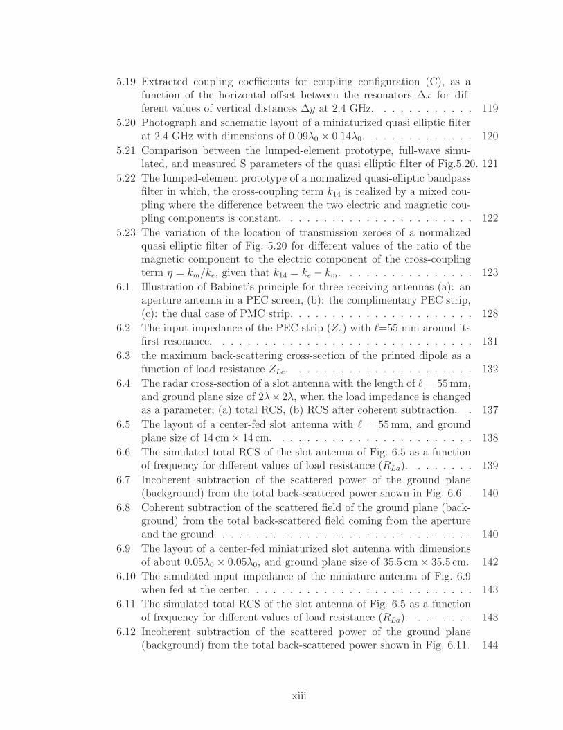
5.19 Extracted coupling coefficients for coupling configuration (C), as afunction of the horizontal offset between the resonators ∆x for dif-ferent values of vertical distances ∆y at 2.4 GHz. . . . . . . . . . . . 119
5.20 Photograph and schematic layout of a miniaturized quasi elliptic filterat 2.4 GHz with dimensions of 0.09λ0 × 0.14λ0. . . . . . . . . . . . . 120
5.21 Comparison between the lumped-element prototype, full-wave simu-lated, and measured S parameters of the quasi elliptic filter of Fig.5.20. 121
5.22 The lumped-element prototype of a normalized quasi-elliptic bandpassfilter in which, the cross-coupling term k14 is realized by a mixed cou-pling where the difference between the two electric and magnetic cou-pling components is constant. . . . . . . . . . . . . . . . . . . . . . . 122
5.23 The variation of the location of transmission zeroes of a normalizedquasi elliptic filter of Fig. 5.20 for different values of the ratio of themagnetic component to the electric component of the cross-couplingterm η = km/ke, given that k14 = ke − km. . . . . . . . . . . . . . . . 123
6.1 Illustration of Babinet’s principle for three receiving antennas (a): anaperture antenna in a PEC screen, (b): the complimentary PEC strip,(c): the dual case of PMC strip. . . . . . . . . . . . . . . . . . . . . . 128
6.2 The input impedance of the PEC strip (Ze) with =55 mm around itsfirst resonance. . . . . . . . . . . . . . . . . . . . . . . . . . . . . . . 131
6.3 the maximum back-scattering cross-section of the printed dipole as afunction of load resistance ZLe. . . . . . . . . . . . . . . . . . . . . . 132
6.4 The radar cross-section of a slot antenna with the length of = 55 mm,and ground plane size of 2λ× 2λ, when the load impedance is changedas a parameter; (a) total RCS, (b) RCS after coherent subtraction. . 137
6.5 The layout of a center-fed slot antenna with = 55 mm, and groundplane size of 14 cm × 14 cm. . . . . . . . . . . . . . . . . . . . . . . . 138
6.6 The simulated total RCS of the slot antenna of Fig. 6.5 as a functionof frequency for different values of load resistance (RLa). . . . . . . . 139
6.7 Incoherent subtraction of the scattered power of the ground plane(background) from the total back-scattered power shown in Fig. 6.6. . 140
6.8 Coherent subtraction of the scattered field of the ground plane (back-ground) from the total back-scattered field coming from the apertureand the ground. . . . . . . . . . . . . . . . . . . . . . . . . . . . . . . 140
6.9 The layout of a center-fed miniaturized slot antenna with dimensionsof about 0.05λ0 × 0.05λ0, and ground plane size of 35.5 cm × 35.5 cm. 142
6.10 The simulated input impedance of the miniature antenna of Fig. 6.9when fed at the center. . . . . . . . . . . . . . . . . . . . . . . . . . . 143
6.11 The simulated total RCS of the slot antenna of Fig. 6.5 as a functionof frequency for different values of load resistance (RLa). . . . . . . . 143
6.12 Incoherent subtraction of the scattered power of the ground plane(background) from the total back-scattered power shown in Fig. 6.11. 144
xiii

6.13 Coherent subtraction of the scattered field of the ground plane (back-ground) from the total back-scattered field of the miniaturized antennaof Fig. 6.9. . . . . . . . . . . . . . . . . . . . . . . . . . . . . . . . . . 145
6.14 High-impedance measurement setup for measuring the input impedanceof the miniaturized slot antenna of Fig. 6.9. . . . . . . . . . . . . . . 146
6.15 The input impedance of the high impedance miniaturized slot antennaof Fig. 6.9 measured using the setup of Fig. 6.14. . . . . . . . . . . . 146
6.16 Schematics of the equivalent circuit of the high-impedance antennaof Fig. 6.9 extracted by the impedance analyzer along with the linedeembedding scheme. . . . . . . . . . . . . . . . . . . . . . . . . . . . 147
6.17 The measured input impedance of the high-impedance miniaturizedslot antenna of Fig. 6.9 after deembedding the effect of the microstrip-line. . . . . . . . . . . . . . . . . . . . . . . . . . . . . . . . . . . . . 148
A.1 Slot antenna in a perfectly conducting ground plane center fed by atwo-wire transmission line. . . . . . . . . . . . . . . . . . . . . . . . . 157
A.2 The geometry of a standard slot antenna along with its principle E-and H-planes. . . . . . . . . . . . . . . . . . . . . . . . . . . . . . . . 161
A.3 The simulated radiation pattern of a slot antenna on air with an infiniteground plane using IE3D with magnetic current discretization. . . . . 163
A.4 The simulated radiation pattern of a slot antenna with an infiniteground plane over an infinite extent dielectric substrate with εr = 2.2and thickness of 0.7874 mm using IE3D with magnetic current dis-cretization. . . . . . . . . . . . . . . . . . . . . . . . . . . . . . . . . 164
A.5 Comparison between the simulated radiation patterns of a finite groundplane slot with no dielectric substrate, obtained from IE3D (electriccurrent discretization) and HFSS. . . . . . . . . . . . . . . . . . . . . 165
A.6 The simulated radiation pattern of a slot antenna with a finite groundplane on a dielectric substrate using IE3D. . . . . . . . . . . . . . . . 166
A.7 The simulated radiation pattern of a slot antenna with a finite groundplane and finite dielectric substrate obtained from HFSS. . . . . . . . 167
xiv

CHAPTER 1
Introduction
1.1 Motivation and Background
Antennas are among the most important components of a wireless network, and
as far as efficiency and size are concerned, they may impose stringent restrictions on
the size and performance of any wireless system. With recent advances in solid-state
devices and MEMS technology, construction of high performance miniaturized trans-
mit and receive modules are now realizable. Although significant efforts have been
devoted towards achieving low-power miniaturized electronic and RF components, is-
sues related to design and fabrication of efficient, miniaturized, and easily integrable
antennas have been overlooked. This remains true not only for antennas but also
for all passive distributed microwave components such as resonators, filters and cou-
plers whose dimensions are comparable or larger than a wavelength. This wavelength
dependence stems from the fact that all of the aforementioned distributed compo-
nents are composed of one or more resonant structures. The main objective of this
dissertation is to embark on the challenging issue of antenna and microwave filter
miniaturization to ultimately realize the holy grail of the next generation of wire-
less systems; that is, the idea of integrating antennas on a chip with the rest of the
transceiver circuitry.
1
In addition to the need for miniaturization, low-power characteristics of such trans-
mit/receive modules are extremely important and require highly efficient low-loss
miniaturized components. In order to reach minimum power consumptions in the
micro-circuits, high-impedance solid-state devices are preferred since they are less-
expensive due to their smaller size. As the size of micro/nano-devices decreases, the
bias current and DC power consumption are reduced. Meanwhile, the impedance of
these devices increases drastically. For example, the motional resistance of MEMS
resonators is on the order of a few kilo-ohms, which necessitates at least an order of
magnitude larger input and output termination impedances so that their superb per-
formance can be fully exploited and accurately measured. Obviously, if a miniaturized
antenna is sought for integration with MEMS transceivers, it should demonstrate very
high input impedance characteristics so as to be compatible with the MEMS circuitry.
Therefore, a high-impedance miniature antenna is desired for such applications.
The use of high-impedance miniature antennas is not limited to the front-end of
microsystems. These antennas may also be used in conjunction with nano-scale de-
vices such as Carbon Nano Tube (CNT) transistors or nano-scale MOSFETs. CNT
transistors are emerging as new high-speed low power nano-scale transistors. It is
predicted that these devices would be extremely fast due to the ballistic transport of
electrons inside the nano-tube, and that they demonstrate very low parasitic capac-
itances (in the order of several aF1). Yet, there is no report on the high-frequency
operation of these devices. One reason is that they have a very high-impedance
(≈ 5kΩ), and thus, they are extremely difficult to test and measure at RF. One way
of utilizing these high-impedance devices is to use them in conjunction with high-
impedance miniature antennas developed in this research. By doing so, we can also
make these nano devices of practical use in new arenas. It is also important to have
a compact and high-impedance antenna that can be matched directly to small size
110−18F
2
(minimum feature size) transistors to keep power consumption at a minimum.
In the context of the above examples, the design and fabrication of highly-efficient
miniaturized antennas and microwave filters are of a great interest. By adding the
high-impedance feature to miniature antenna characteristics, one of the major issues
of nano-scale devices, especially at higher frequencies, can be resolved. Thus, these
miniaturized components, together with micro/nano-scale sensors and transducers,
may find numerous applications in industry, medicine, and the military.
The subject of small antennas is not new. The literature addressing this subject
dates back to the early 1940’s. The early studies of small antennas, however, were
restricted to the establishment of the fundamental limitations of this class of antennas,
where features such as bandwidth, gain, and efficiency have analytically been related
to the antenna size [1, 2, 3]. Using a multi-pole expansion and a clever equivalent
circuit model, Chu was able to derive the Q factor of the equivalent circuit for each
spherical mode in terms of the normalized radius (a/λ) of the smallest sphere enclosing
the antenna structure. Also, it is shown that the Q of the lowest order mode is a
lower bound for the Q of a single resonant antenna. Qualitatively, these studies show
that for single resonant antennas, the smaller the maximum dimension of an antenna,
the higher its Q, or equivalently, the lower its bandwidth. Nevertheless, no discussion
is provided in the above literature about small antenna topologies, and its impedance
matching.
In recent years, practical aspects of antenna miniaturization have received signifi-
cant attention. Most successful designs rely on the use of high-permittivity ceramics,
which are not suitable for monolithic integration. Moreover, this approach is prone to
surface-wave excitation at higher frequencies. Another approach for antenna minia-
turization, reported in the literature, is to use meandered-line antennas, in which a
half wavelength antenna is made compact by meandering the line. In general, me-
andered antennas have considerable ohmic losses, and hence, must be fabricated on
3
high-temperature superconductive films.
Another approach for designing small antennas is to find a miniaturized topol-
ogy with a minimal ohmic loss and an appropriate characteristic impedance. In
accordance with this premise, a novel class of miniaturized slot topology is intro-
duced. Variation of this topology has been extensively employed to design a variety
of efficient miniaturized antennas, high-Q microwave filters, and resonators. The pro-
posed miniature slot topology, when used for antenna design, demonstrates a much
less ohmic loss, and thus, higher efficiency than meandered microstrip structures.
When used for resonator/filter miniaturization, the application of miniaturized slot-
line topology leads to a much higher Q, or equivalently, lower insertion loss than
that of microstrip filters. This miniaturized topology also demonstrates the high-
impedance property required for some micro- and nano-devices.
Miniature antennas, as alluded to briefly in the earlier discussion, are inherently
narrow band, where the bandwidth is subject to a fundamental limit. At the first
glance, the bandwidth limit might seem to be intractable, whereas is not the case
for planar antennas. In other words, the fundamental limit introduces a loose upper
bound on the bandwidth of a planar antenna. For three dimensional antennas, in
contrast, the attainable bandwidth can get closer to the fundamental limit. As a
result, a considerable improvement in the bandwidth of planar antennas might be
still possible without violating the fundamental limit.
The bandwidth of miniaturized antennas can be improved more effectively if we
understand the causes of their narrow bandwidth. The radiation conductance of a
slot antenna is an equivalent quantity, whose dissipated power models the radiated
power by the antenna. Likewise, the radiation resistance of wire and printed antennas
is defined. The radiation resistance does not contribute to the overall loss of the
antenna. Instead, it indicates how effectively an antenna may perform. Moreover,
radiation resistance/conductance determines the radiation quality factor, defined as
4
Qrad = 1/∆, where ∆ is the fractional bandwidth of the antenna. For the slot
structure, radiation conductance is proportional to the length of the slot line. As the
miniaturization increases, the radiation conductance decreases, and thus, it leads to a
higher Qrad and a lower antenna bandwidth. If the physical aperture of a slot antenna
is increased in such a way that its overall dimensions remain the same, the radiation
conductance as well as the bandwidth increases. Based on the above premise, a
miniaturized folded-slot topology is introduced whose radiation conductance is four
times as much as that of an unfolded miniaturized slot topology, while having almost
the same dimensions.
Another factor limiting the bandwidth of small antennas is the required match-
ing network, which turns out to be narrow-band by itself. As mentioned earlier,
the radiation conductance of a miniaturized slot is very small, where it translates
into a very high input impedance. Matching such a high-impedance to a standard
50Ω line is rather difficult and should be done off-resonance. At an off-resonant fre-
quency, however, the reactance slope of the antenna impedance is very high, and
therefore, matching would be narrow band. To alleviate this problem, namely, rapid
variation of the input resistance and reactance with respect to frequency, the idea
of self-complementarity may be tried. The input impedance of a self-complimentary
antenna, in an ideal case, is a frequency-independent real quantity. A few conditions
must be satisfied by a self-complementary structure. The first condition is that the
structure should be of an infinite extent. Obviously, this condition is contradictory to
the notion of miniaturization and will be treated so that an economical compromise
may be reached.
Another major thrust of this research pertains to the design and miniaturization
of passive microwave resonators and filters. A few approaches in the literature ad-
dress filter miniaturization, among which are the use of lumped-element filters, high-
temperature super conducting (HTS) filters, and slow-wave distributed resonators
5

[4, 5]. Although filters designed using lumped-elements can be made very small, their
insertion loss becomes prohibitively large at UHF and beyond. The power handling
capability of lumped-element filters may also be very poor at high frequencies. To
cope with the insertion loss and probably power handling problems, high-temperature
super-conducting filters (HTS) have been proposed, which can play an important
role in communication systems if the cost issue is resolved [6]. In addition to the
cost and complexity associated with the HTS circuits, superconductivity has not yet
been demonstrated at room temperature. Cooling systems and their power require-
ments make the current HTS technology inapplicable for mobile wireless systems
[7]. Distributed element approaches in miniaturized filter design, such as coupled
transmission-line resonators, exhibit far superior performance with regard to the in-
sertion loss and power handling capabilities compared to lumped-element filters. On
the other hand, size and complexity are tow major drawbacks of distributed element
filters.
The prevalent idea throughout this dissertation is to implement a novel and ef-
ficient miniaturized topology suitable to design miniaturized distributed microwave
resonators and filters. The building block of the proposed topology for miniature
resonators is similar to the one used for miniaturized antennas. The miniature res-
onators, on one hand, are conducive to the design of miniaturized antennas when the
impedance of these resonators are matched to that of the standard transmission-line.
On the other hand, the appropriate coupling between these miniaturized resonators,
through adjusting their distance and orientation with respect to each other, would
lead to miniaturized direct-coupled bandpass filters. Additionally, the proposed res-
onators allow for both electric and magnetic coupling –also referred to as negative
and positive coupling– and thus, enabling the design of elliptical and quasi-elliptical
filters. Quasi-elliptical filters are very compact, and at the same time, provide a very
sharp out of band rejection due to the existence of two out-of-band transmission zeros.
6

Having successfully introduced novel miniaturized topologies for antenna, res-
onator, and filter applications, issues related to the integration of these components
to the active electronics and circuitry must be addressed. As mentioned earlier, one
of the restrictions in the integration process is the ultra high impedance of the elec-
tronics as well as micro- and nano-devices. The standard characteristic impedance
adopted for RF applications is 50Ω, which makes it impossible to be matched directly
to low-power high-impedance electronics with the use of ordinary matching networks.
Conversely, significant effort has been devoted to modifying the electronic devices
so as to reduce their input impedance level. In doing so, the size and cost of such
a devise, as well as its power consumption, would increase considerably. Another
difficulty in dealing with high-impedance structures is that their performance cannot
be accurately measured at RF since microwave measurement instruments are also
designed to work well for impedances in the same order of magnitude as the standard
impedance. All of the above ramifications remain true for micro- and nano-scale de-
vices. Thus, the high-impedance miniature antenna introduced in this research may
find numerous applications in the area of micro- and nano-systems.
In the future, this research can be pursued in a number of different directions,
some of which are immediate extensions, while others can be a part of a longer term
plan. A few of the short term extensions of this work include the use of the proposed
miniaturized topology in almost any application, in which a resonant structure such
as antenna, resonator, and filter is required. Array configuration of miniaturized
antennas for automotive and radar applications, frequency selective surfaces, and
lenses can lead to much smaller wireless and radar systems. Multi-functional and
reconfigurable miniaturized and tunable antennas and resonators are among other
areas where the contribution of this thesis may find prospective applications. In the
long run, the high-impedance feature of the proposed miniature antenna can find
numerous applications in conjunction with the emerging high-impedance nano-scale
7
devices in interfacing, impedance matching, and testing.
1.2 Thesis Overview
The primary objective of this thesis is to introduce a power efficient miniaturized
solution for mobile wireless systems. This task has been divided into three main
thrusts. The first thrust addresses issues related to the design and fabrications of
miniaturized antennas. A great amount of attention is devoted to different aspects of
this task, such as miniaturizing the antenna topology, enhancing the antenna band-
width, and introducing the complementary and self-complementary realization of the
same topology (Chapters 2,3,4). The second thrust addresses the design of minia-
turized high-Q resonators and RF filters, which will be presented in Chapter 5. The
last piece of this work touches on the interfacing of the miniaturized antennas to the
high-impedance electronics, MEMS, and nano-devices (Chapter 6). In more details,
the outline of this thesis is as follows.
In Chapter 2, a UHF miniaturized planar antenna is introduced. This antenna
consists of a quarter-wavelength resonant slot-line. The resonance is established by
means of an open- and a short-circuit at both ends of the slot-line. Short-circuit termi-
nation for a slot-line is readily realizable due to the presence of the ground plane. The
open-circuit termination, however, can only be realized using distributed elements by
employing two coiled quarter-wave short-circuited slot lines. Further miniaturization
is made possible through additional modification of the antenna topology so as to use
the two dimensional area more efficiently. As a result, a miniaturized UHF planar
slot antenna with dimensions of 0.12λ0 × 0.12λ0 is achieved.
Chapter 3 demonstrates a novel approach for the miniaturization of slot antennas.
The antenna design in Chapter 2 was based on the realization of an open and a short
boundary condition at each end of the slot-line, which can only provide a quarter-wave
8

antenna. The basic premise of this chapter is to implement variable reactive bound-
ary conditions instead of open-circuit or short-circuit terminations. The advantages
of reactive boundary conditions are twofold. One advantage is that the symmetry
of the antenna structure is preserved; the other is that much smaller antennas than
a quarter-wavelength are feasible. The overall area occupied by this antenna can be
precisely controlled by adjusting reactive boundary conditions at both ends of the
slot-line. The application of such loads is shown to reduce the size of the resonant
slot antenna for a given resonant frequency, without imposing any stringent condition
on its impedance matching. The matching procedure is based on an equivalent circuit
model for the antenna and its feed structure. The corresponding equivalent circuit
parameters are extracted using a full-wave forward model in conjunction with a Ge-
netic Algorithm (GA) optimizer. These parameters are employed to find a proper
matching network to a 50 Ω line. It is shown in this chapter that for a prototype slot
antenna with approximate dimensions of 0.05λ0 × 0.05λ0, the impedance match is
obtained with a fairly high gain of −3 dBi, for a very small rectangular ground plane
(≈ 0.20λ0 × 0.20λ0).
Chapter 4 delineates methodologies to enhance the bandwidth of miniaturized
antennas. These methods include the application of folded and self-complementary
structures, both of which are shown to be very effective for bandwidth improvement.
The miniaturized folded-slot topology is demonstrated to enhance the bandwidth
of the miniaturized slot antenna of Chapter 3 by more than 100%. The radiation
conductance of a miniaturized folded-slot topology is four times larger than that of
a miniaturized slot antenna, and thus, it is much easier to match to a 50Ω line.
Furthermore, the higher the radiation conductance, the lower the Q and the higher
bandwidth can be expected.
Another methodology described in this chapter is to utilize the concept of self-
complementarity to achieve a wider bandwidth. In theory, self-complementary struc-
9
tures must be of infinite extent in order to behave as a frequency independent an-
tenna. Nevertheless, a compromise can be made between the size (truncation) and the
bandwidth. In the first example of self-complementary design, a self-complementary
miniaturized folded antenna is presented, where it shows more than 20% bandwidth
increase over the folded-slot of the same size. The next example of this chapter deals
with an H-shaped self-complementary antenna, in which the miniaturization criterion
has been relaxed in favor of bandwidth. The H-shape antenna demonstrates a very
wide -10 dB return loss bandwidth of 2.3:1 and a fairly constant gain of slightly above
1 dBi over the entire band of operating frequency. The dimensions of this antenna
are 0.13λ0 × 0.24λ0 at the lowest frequency of operation.
The focus of the second thrust of this thesis is RF filter miniaturization, which
is the topic of Chapter 5. In this chapter, both miniaturized slot-line and folded-slot
resonators are used to design different types of direct- and cross-coupled filters. Cou-
pling between the adjacent resonators is extracted using the pole-splitting method
with the aid of a full-wave EM simulator. Having extracted the coupling coefficients,
design curves can be generated, and the filter theory may be employed to design
different bandpass filters. The size of introduced miniaturized filters is shown to be
very small compared to that of conventional transmission-line filters, without com-
promising their insertion loss drastically. The Q of the proposed slot-line filters is
demonstrated to be considerably higher than that of microstrip resonators of the same
size. Also in this chapter, a rigorous study will be conducted on the effect of resonator
parameters such as size and impedance on the unloaded Q of the structure.
The third part of this thesis deals with the interfacing of miniature antennas
and high-impedance electronics, micro and nano-devices for wireless communication
systems. Chapter 6 is an effort to address the issue of high-impedance antenna match-
ing, which seems to be critical for nanotechnology, especially at high frequencies. The
approach adopted in this chapter is to control the impedance of the miniaturized an-
10

tenna so that it can be matched directly to a high-impedance load without a need to
any type of external matching network. This load can be an input stage of an LNA,
a bank of MEMS filters, or a CNT transistor. Having designed a high-impedance
miniature antenna, the impedance of the antenna needs to be measured. Available
microwave measurement instruments are designed to work with the standard 50 Ω
systems. Nevertheless, an alternative measurement technique is required for high-
impedance antennas. Chapter 6 introduces a new technique to measure the radiation
resistance of high-impedance antennas. In this technique, first a relationship is estab-
lished between the terminating impedance of a miniature antenna and its radar cross
section (RCS). Also, the condition on RCS for the matched impedance is derived.
Then, an antenna under test is terminated with a set of terminating impedances,
and its RCS is measured. The antenna impedance can be identified when the RCS
satisfies the condition for that of a matched antenna. This technique is, then, em-
ployed to measure the input impedance of the high-impedance miniature slot antenna
presented in this research.
Finally, Chapter 7 summarizes the contributions presented in this thesis and sub-
mits recommendations for the future work.
11

CHAPTER 2
A Compact Quarter-wavelength
Slot Antenna Topology
2.1 Introduction
With the advent of wireless technology and ever increasing demand for high data
rate mobile communications, the number of radios on military mobile platforms has
reached to a point that the real estate for these antennas has become a serious issue.
Similar problems are also emerging in the commercial sector where the number of
wireless services planned for future automobiles, such as FM and CD radios, analog
and digital cell phones, GPS, keyless entry and etc., is on the rise. To circumvent
the aforementioned difficulties to some extent, antenna miniaturization and/or com-
pact multi-functional antennas must be considered. Such architectural antennas are,
therefore, of great importance in mobile communication systems where low visibility
and high mobility are required. Slot radiating elements, having a planar geometry
and being capable of transmitting vertical polarization when placed nearly horizon-
tal, are specifically appropriate for these applications. Moreover, slot antennas have
another useful property so far as impedance matching is concerned. Slot dipoles can
easily be excited by a microstrip line and can be matched to arbitrary line impedances
12
simply by moving the feed point along the slot. Slot structure seems to satisfy most
requirements of mobile communication systems, and consequently, it is chosen as a
suitable candidate to design miniaturized antennas.
The subject of antenna miniaturization is not new. The literatures concerning
this subject date back to the early 1940’s [8, 1]. To our knowledge the fundamental
limitations of small antennas was first addressed by Chu in 1948 [1]. Using a multi-
pole expansion and a clever equivalent circuit model, Chu was able to derive the Q
factor of the equivalent circuit for each spherical mode in terms of the normalized
radius (a/λ) of the smallest sphere enclosing the antenna. In [1] it is also shown
that the Q of the lowest order mode is a lower bound for the Q of a single resonant
antenna. This subject was revisited by Wheeler [9], Harrington [3], and Collins [10].
In [10] a similar procedure is used for characterization of a small dipole antenna
using cylindrical wave functions. Then, a cylindrical enclosing surface is used which
produces a tighter lower bound for the Q of small antennas with large aspect ratios
such as dipoles and helical antennas. Qualitatively, these studies show that for single
resonant antennas, the smaller is the maximum dimension of an antenna, the higher
is its Q or equivalently the lower is its bandwidth [2]. However, in these papers
no discussion is provided about the miniaturization methods, antenna topology, or
impedance matching.
Considering the wave propagation issues where line-of-sight communication is an
unlikely event, such as in an urban environment or over irregular terrain, carrier fre-
quencies at HF-UHF band are commonly used. At these frequencies there is consider-
able penetration through vegetation and buildings, wave diffraction around obstacles,
and wave propagation over curved surfaces. However, at these frequencies the size of
efficient antennas are relatively large and therefore a large number of such antennas
may not fit in the available space without the risks of mutual coupling and co-cite
interference. Efficient antennas require dimensions of the order of half a wavelength
13
for single frequency operation. To cover a wide frequency range, broadband antennas
may be used, however, dimensions of these antennas are comparable to or larger than
the wavelength at the lowest frequency. Besides, depending on the applications, the
polarization and the direction of maximum directivity for different wireless systems
operating at different frequencies may be different and hence a single broadband an-
tenna may not be sufficient. It should also be noted that any type of broadband
antenna is highly susceptible to electronic warfare jamming techniques. Variations of
monopole and dipole antennas in use today are prohibitively large and bulky at HF
through VHF, and therefore, efforts to achieve miniaturized antennas are inevitable.
In subsequent sections, the topology of an efficient, miniaturized, resonant slot
antenna is presented, and then, its input impedance, bandwidth, and radiation char-
acteristics are investigated. This class of antennas can exhibit simultaneous band
selectivity and anti-jam characteristics in addition to possessing a planar structure
and low profile, which is easily integrable with other RF and microwave circuits.
2.2 Compact Spiral Antennas
Equiangular and Archimedean spiral antennas [11] are commonly used as broad-
band antennas. These antennas usually have arm length larger than a wavelength.
Not much has been reported about the performance of spiral antennas when the arm
length is half of the guided wavelength (a resonance condition). One obvious reason
is that slot spiral antennas are usually center-fed where at the first resonance the in-
put impedance is very high, and impedance matching becomes practically impossible.
However, if we allow the feed point to be moved to one end of the arm, impedance
matching to transmission lines with typical characteristic impedances seems possible.
First an equiangular spiral slot, as shown in Fig. 2.1(a), was considered. Using
electrostatic analysis, the guided wavelength of a slot-line with finite ground plane
14
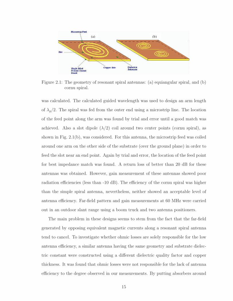
(a) (b)
Figure 2.1: The geometry of resonant spiral antennas: (a) equiangular spiral, and (b)cornu spiral.
was calculated. The calculated guided wavelength was used to design an arm length
of λg/2. The spiral was fed from the outer end using a microstrip line. The location
of the feed point along the arm was found by trial and error until a good match was
achieved. Also a slot dipole (λ/2) coil around two center points (cornu spiral), as
shown in Fig. 2.1(b), was considered. For this antenna, the microstrip feed was coiled
around one arm on the other side of the substrate (over the ground plane) in order to
feed the slot near an end point. Again by trial and error, the location of the feed point
for best impedance match was found. A return loss of better than 20 dB for these
antennas was obtained. However, gain measurement of these antennas showed poor
radiation efficiencies (less than -10 dB). The efficiency of the cornu spiral was higher
than the simple spiral antenna, nevertheless, neither showed an acceptable level of
antenna efficiency. Far-field pattern and gain measurements at 60 MHz were carried
out in an outdoor slant range using a boom truck and two antenna positioners.
The main problem in these designs seems to stem from the fact that the far-field
generated by opposing equivalent magnetic currents along a resonant spiral antenna
tend to cancel. To investigate whether ohmic losses are solely responsible for the low
antenna efficiency, a similar antenna having the same geometry and substrate dielec-
tric constant were constructed using a different dielectric quality factor and copper
thickness. It was found that ohmic losses were not responsible for the lack of antenna
efficiency to the degree observed in our measurements. By putting absorbers around
15
the feed cable and antenna positioner, it was found that these antennas produce a
very strong near-field which can excite current on the nearby objects, such as the
cable feeding them and the antenna positioner. The current induced on these objects
in turn radiated the input power, but not necessarily in the direction of the maximum
antenna radiation pattern. Thus, it can be discerned that the observed impedance
match is owing to the near-field coupling to the feeding cable. Obviously, when the
cable is shielded, the matching is deteriorated. This conclusion is consistent with our
expectation that the antenna should be hard to match mainly due to the presence of
opposing equivalent magnetic currents on the spiral.
2.3 A Miniature Quarter-wave Topology
A different topology for a miniaturized resonant slot is sought that does not have
the drawbacks of the previously discussed spiral and cornu-spiral geometries. A major
reduction in size is achieved by noting that a slot dipole can be considered as trans-
mission line resonator where at the lowest resonant frequency the magnetic current
(transverse electric field in the slot) goes to zero at each end of the dipole antenna.
As mentioned before, at this frequency the antenna length is equal to λg/2 where λg
is the wavelength of the quasi-TEM mode supported by the slot-line. λg is a function
of the substrate thickness, dielectric constant, and slot width, which is shorter than
the free-space wavelength. In view of transmission line resonators, one can also make
a quarter-wave resonator by creating a short circuit at one end and an open circuit at
the other end. Creating a physical open circuit, however, is not practical for slot-lines.
The new design borrows the idea of the non-radiating tightly-coiled slot spiral from
the previous design. Basically, a spiral slot of a quarter wavelength and short-circuited
at one end behaves as an open circuit at the resonant frequency. Therefore, a quarter-
wave slot-line, that is short-circuited at one end and terminated by the non-radiating
16
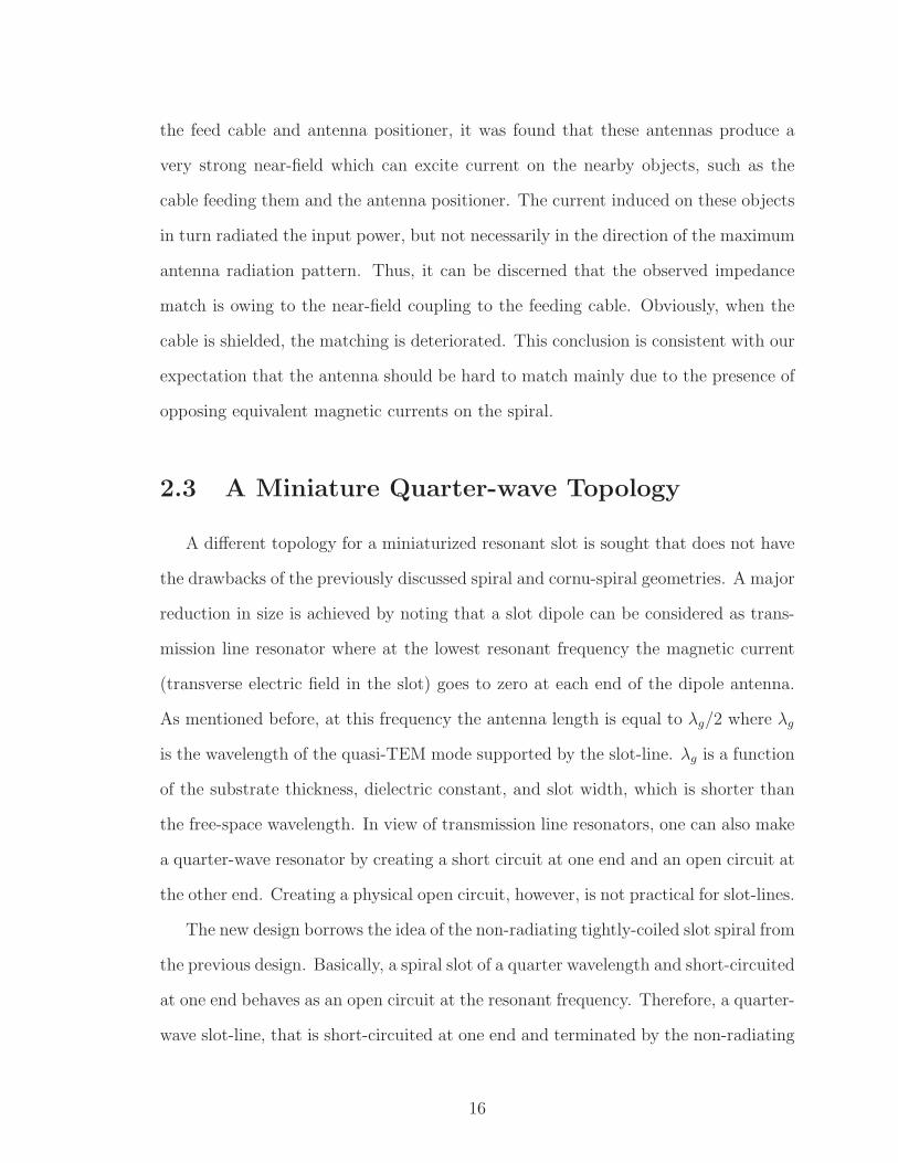
6.5 cm
6.5 cm
Figure 2.2: The magnetic current distribution on the UHF miniaturized slot antennaat the resonance frequency (600 MHz). The figure shows the ground-planeside of the antenna and the meshing configuration used in the method ofmoments calculations.
quarter-wave spiral at the other end, should resonate and radiate electromagnetic
waves very efficiently. With this topology, the size of the slot dipole can be reduced
by approximately 50%. Further size reduction can be accomplished by bending the
radiating section. This bending procedure should be done so that no section of the
resulting line geometry carries a magnetic current opposing the current on any other
sections.
Fig. 2.2 shows the geometry of a typical λg/4 compact resonating slot antenna.
The radiating section is terminated with two identical quarter-wave non-radiating
spiral slots to maintain the symmetry. It was found that by splitting the magnetic
current at the end into equal and opposing magnetic currents, the radiation pattern
is enhanced. Since the magnetic current distribution attains its maximum at the end
of the quarter-wave line, the magnetic current in the beginning segments of a single
(unbalanced) quarter-wave spiral reduces the radiation of the radiating section. But
17

Figure 2.3: Electric current distribution on the microstrip feed of the slot antenna atthe resonant frequency.
the opposite magnetic currents on two such spirals simply cancel the radiated field of
each other, and as a result, the radiated field of the radiating section remains intact.
Additional miniaturization can also be achieved by noting that the strength of the
magnetic current near the short-circuited end of the radiating section is insignificant.
Hence, bending this section of the line does not significantly reduce the radiation
efficiency despite allowing opposing currents. In Fig. 2.2 the T-top represents a small
reduction in the length of the line without affecting the radiation efficiency.
This antenna is fed by an open-ended microstrip line shown in Fig. 2.3. A quarter
wavelength line corresponds short-circuit line under the slot, however, using the length
of the microstrip line as an adjustable parameter, the reactive part of the antenna
input impedance can be compensated for. Figures 2.2 and 2.3, respectively, show
the simulated electric current distribution on the microstrip feed and the magnetic
current distribution on the slot of the compact UHF antenna designed to operate at
600 MHz. For this design we chose an ordinary FR4 substrate with a thickness of
3 mm (120 mil) and a dielectric constant of εr = 4. A full-wave moment method
software was used for the simulations of this antenna [12].
The microstrip feed is constructed from two sections: 1) a 50 Ω line section, and
2) an open-ended 80 Ω line. The 80 Ω line is thinner which allows for compact and
18
localized feeding of the slot. The length of this line is adjusted to compensate for the
reactive component of the slot input impedance. Noting that the slot appears as a
series load in the microstrip transmission line, a line length of less than λm/4 compen-
sates for an inductive reactance, and a line length of longer than λm/4 compensates
for a capacitive reactance, where λm is the guided wavelength on the microstrip line.
In the process of impedance matching, the length of the microstrip line feeding
the slot was first set equal to a quarter-wavelength so that the the characteristic
impedance of the slot antenna can be identified. Through this simulation, it was
found that the slot antenna fed near the edge is inductive. Therefore, a length less
than λm/4 is chosen for the open-ended microstrip line to compensate for the inductive
input impedance. The real part of the input impedance of a slot dipole depends on the
feed location along the slot and increases from zero at the short-circuited end to about
2000 Ω at the center (quarter wavelength from the short circuit). This property of the
slot dipole allows for matching to almost all practical transmission line impedances.
The crossing point of the microstrip line over the slot was determined using the full-
wave analysis tool by trial-and-error. The uniform current distribution over the 50 Ω
line section, as shown in Fig. 2.3, indicates no standing wave pattern, which is a result
of a very good input impedance match.
Apart from the T-top section, the quarter-wave radiating section of the slot dipole
is composed of three slot-line sections, two vertical and one horizontal. Significant
radiation emanates from the middle and lower sections. Changing the relative size of
these two sections controls the polarization of the proposed antenna. In this design,
the relative lengths of the three line sections were chosen in order to minimize the
area occupied by the slot structure. The slot width of the first section can as well be
varied in order to enhance the impedance matching. When there is a limitation in
moving the microstrip and slot-line crossing point, the slot width may be changed.
At a given point from the short-circuited end, an impedance match to a lower line
19
impedance can be achieved when the slot width is narrowed. This was used in this
design, where the slot-line width of the top vertical section is narrower than those of
the other two sections. It should be pointed out that by narrowing the slot-line width
the magnetic current density increases, but the total magnetic current in the line does
not. In other words, there is no discontinuity in the magnetic current along the line at
points where the slot width is changed, however, there are other consequences. One is
the change in the characteristic impedance of the line, and the second is the change in
the antenna efficiency considering the finite conductivity of the ground plane. There
are two components of electric current flowing on the ground plane; one component
flows parallel to the edge and the other is perpendicular. For narrow slots the current
density of the parallel component near the edge increases, and as a result, this current
sees a higher ohmic resistance. The magnetic current over the T-top section is very
low and does not contribute to the radiated field but its length affects the resonant
frequency. Half the length of the T-top section originally was part of the first vertical
section, which is removed and placed horizontally to lower the vertical extent of the
antenna.
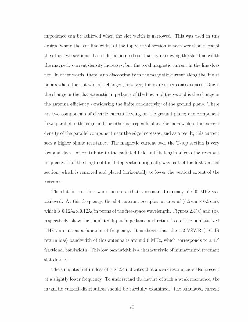
The slot-line sections were chosen so that a resonant frequency of 600 MHz was
achieved. At this frequency, the slot antenna occupies an area of (6.5 cm × 6.5 cm),
which is 0.12λ0×0.12λ0 in terms of the free-space wavelength. Figures 2.4(a) and (b),
respectively, show the simulated input impedance and return loss of the miniaturized
UHF antenna as a function of frequency. It is shown that the 1.2 VSWR (-10 dB
return loss) bandwidth of this antenna is around 6 MHz, which corresponds to a 1%
fractional bandwidth. This low bandwidth is a characteristic of miniaturized resonant
slot dipoles.
The simulated return loss of Fig. 2.4 indicates that a weak resonance is also present
at a slightly lower frequency. To understand the nature of such a weak resonance, the
magnetic current distribution should be carefully examined. The simulated current
20
x=j50
x=-j50
50ocsc
600MHz
575MHz 625MHz
(a)
0.54 0.56 0.58 0.6 0.62 0.64-30
-25
-20
-15
-10
-5
0
5
dB
dB[S(1,1)]
Frequency (GHz)
(b)
Figure 2.4: Simulated reflection coefficient of the miniaturized UHF antenna with aninfinite ground plane. (a) Smith chart representation. (b) Magnitude of|S11| in logarithmic scale.
21
distribution demonstrates that the double spiral terminations are at resonance at
the exact frequency where a weak resonance is observed in the return loss. In this
scenario, the radiating section serves as a feed line for the terminating double spirals,
and the double spirals turn into a radiating element over this frequency band. This
double spiral, which resembles the cornu-spiral of Fig. 2.1(a), is not a very efficient
radiator due to its ohmic losses nor can it be matched easily. That is why the return
loss at this resonance is poor.
The polarization of this antenna may appear to be rather unpredictable at a
first glance due to its convoluted geometry. However, it can be conjectured that the
polarization of any miniaturized antenna whose dimensions are much smaller than a
wavelength cannot be anything other than linear. This is basically because of the fact
that the small electrical size of the antenna does not allow for a phase shift between
two orthogonal components of the radiated field required for producing an elliptical
polarization. Hence by rotating the antenna a desired linear polarization along a
given direction can be obtained.
2.4 Realization and Measurements
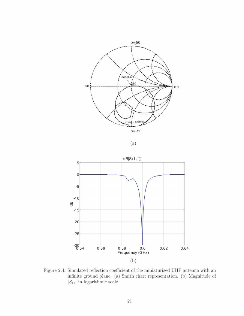
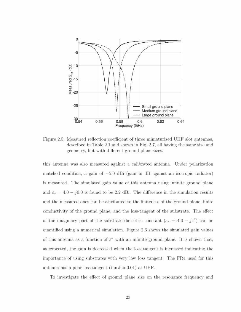
An antenna based on the layout shown in Figs. 2.2 and 2.3 was made on a FR4
printed-circuit-board. In the first try, the size of the ground plane was chosen to
be 8.5 cm × 11.5 cm. The return loss of this antenna was measured with a network
analyzer, and the result is shown by the solid line in Fig. 2.5. It is noticed that the
resonant frequency of this antenna is at 568 MHz, which is significantly lower than
what was predicted by the simulation. Also, the measured return loss for the designed
microstrip feed line (not shown here) was around -10 dB. To get a better return loss,
the length of the microstrip line had to be extended slightly. The measured return
loss of this antenna, after a slight modification, is shown in Fig. 2.5. The gain of
22
0.54 0.56 0.58 0.6 0.62 0.64-30
-25
-20
-15
-10
-5
0
Frequency (GHz)
Mea
sure
d S
11 (
dB)
Small ground plane Medium ground planeLarge ground plane
Figure 2.5: Measured reflection coefficient of three miniaturized UHF slot antennas,described in Table 2.1 and shown in Fig. 2.7, all having the same size andgeometry, but with different ground plane sizes.
this antenna was also measured against a calibrated antenna. Under polarization
matched condition, a gain of −5.0 dBi (gain in dB against an isotropic radiator)
is measured. The simulated gain value of this antenna using infinite ground plane
and εr = 4.0 − j0.0 is found to be 2.2 dBi. The difference in the simulation results
and the measured ones can be attributed to the finiteness of the ground plane, finite
conductivity of the ground plane, and the loss-tangent of the substrate. The effect
of the imaginary part of the substrate dielectric constant (εr = 4.0 − jε′′) can be
quantified using a numerical simulation. Figure 2.6 shows the simulated gain values
of this antenna as a function of ε′′ with an infinite ground plane. It is shown that,
as expected, the gain is decreased when the loss tangent is increased indicating the
importance of using substrates with very low loss tangent. The FR4 used for this
antenna has a poor loss tangent (tan δ ≈ 0.01) at UHF.
To investigate the effect of ground plane size on the resonance frequency and
23
10-4
10-3
10-2
10-1
-12
-10
-8
-6
-4
-2
0
2
4
Sim
ulat
ed G
ain
[ dB
i ]
Dielectric loss tangent (tan δ)
Figure 2.6: Simulated Gain of the UHF miniaturized antenna on an infinite substratewith εr = 4.0 (1 − j tan δ).
25 cm
12 cm11 cm
Figure 2.7: A photograph of three miniaturized UHF antennas, all having the sametopology and dimensions but with different ground plane sizes.
24
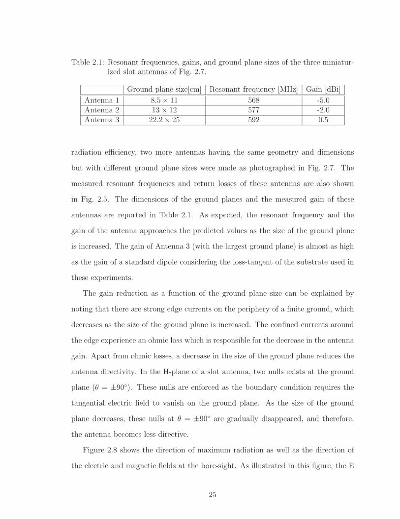
Table 2.1: Resonant frequencies, gains, and ground plane sizes of the three miniatur-ized slot antennas of Fig. 2.7.
Ground-plane size[cm] Resonant frequency [MHz] Gain [dBi]
Antenna 1 8.5 × 11 568 -5.0Antenna 2 13 × 12 577 -2.0Antenna 3 22.2 × 25 592 0.5
radiation efficiency, two more antennas having the same geometry and dimensions
but with different ground plane sizes were made as photographed in Fig. 2.7. The
measured resonant frequencies and return losses of these antennas are also shown
in Fig. 2.5. The dimensions of the ground planes and the measured gain of these
antennas are reported in Table 2.1. As expected, the resonant frequency and the
gain of the antenna approaches the predicted values as the size of the ground plane
is increased. The gain of Antenna 3 (with the largest ground plane) is almost as high
as the gain of a standard dipole considering the loss-tangent of the substrate used in
these experiments.
The gain reduction as a function of the ground plane size can be explained by
noting that there are strong edge currents on the periphery of a finite ground, which
decreases as the size of the ground plane is increased. The confined currents around
the edge experience an ohmic loss which is responsible for the decrease in the antenna
gain. Apart from ohmic losses, a decrease in the size of the ground plane reduces the
antenna directivity. In the H-plane of a slot antenna, two nulls exists at the ground
plane (θ = ±90). These nulls are enforced as the boundary condition requires the
tangential electric field to vanish on the ground plane. As the size of the ground
plane decreases, these nulls at θ = ±90 are gradually disappeared, and therefore,
the antenna becomes less directive.
Figure 2.8 shows the direction of maximum radiation as well as the direction of
the electric and magnetic fields at the bore-sight. As illustrated in this figure, the E
25
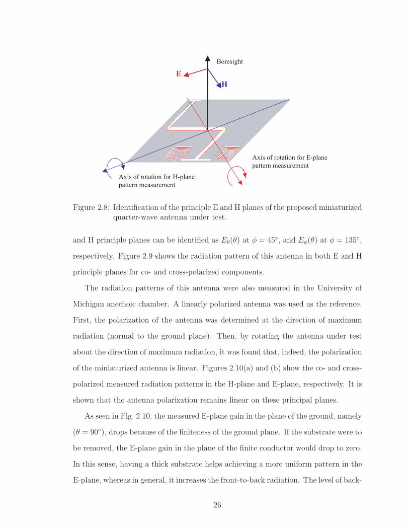
E H
Axis of rotation for E-plane pattern measurement
Axis of rotation for H-plane pattern measurement
Boresight
Figure 2.8: Identification of the principle E and H planes of the proposed miniaturizedquarter-wave antenna under test.
and H principle planes can be identified as Eθ(θ) at φ = 45, and Eφ(θ) at φ = 135,
respectively. Figure 2.9 shows the radiation pattern of this antenna in both E and H
principle planes for co- and cross-polarized components.
The radiation patterns of this antenna were also measured in the University of
Michigan anechoic chamber. A linearly polarized antenna was used as the reference.
First, the polarization of the antenna was determined at the direction of maximum
radiation (normal to the ground plane). Then, by rotating the antenna under test
about the direction of maximum radiation, it was found that, indeed, the polarization
of the miniaturized antenna is linear. Figures 2.10(a) and (b) show the co- and cross-
polarized measured radiation patterns in the H-plane and E-plane, respectively. It is
shown that the antenna polarization remains linear on these principal planes.
As seen in Fig. 2.10, the measured E-plane gain in the plane of the ground, namely
(θ = 90), drops because of the finiteness of the ground plane. If the substrate were to
be removed, the E-plane gain in the plane of the finite conductor would drop to zero.
In this sense, having a thick substrate helps achieving a more uniform pattern in the
E-plane, whereas in general, it increases the front-to-back radiation. The level of back-
26
-180 -135 -90 -45 0 45 90 135 180-50
-45
-40
-35
-30
-25
-20
-15
-10
-5
0
θ [degree]
Sim
ulat
ed R
adia
tion
Pat
tern
[dB
]
E-plane, co-polH-plane, co-polE-plane, x-polH-plane, x-pol
Figure 2.9: Simulated radiation pattern of the miniaturized quarter-wave antenna forboth E- and H- planes.
radiation also depends on the size of the ground plane; that is, the smaller the ground
plane, the higher is the back-radiation. When no dielectric substrate is present (εr =
1), the radiation from the upper and lower magnetic currents completely cancel each
other in the plane of the perfect conductor, creating a null in the E-plane radiation
pattern. However, because of the presence of the substrate and depending on its
thickness and relative dielectric constant, a perfect cancellation does not occur. This
explains the discrepancies observed between the measured and predicted radiation
patterns (for infinite ground plane). Since the thickness of the substrate is only a
small fraction of the wavelength, almost similar gain values are measured in the upper
and lower half-spaces. A more comprehensive discussion on the effect of finite ground
plane will be presented in the next chapter, where a novel approach for miniaturization
of resonant slot antennas is proposed.
It is worth mentioning that further miniaturization can easily be accomplished by
increasing the dielectric constant of the substrate. In this case, the guide wavelength
27
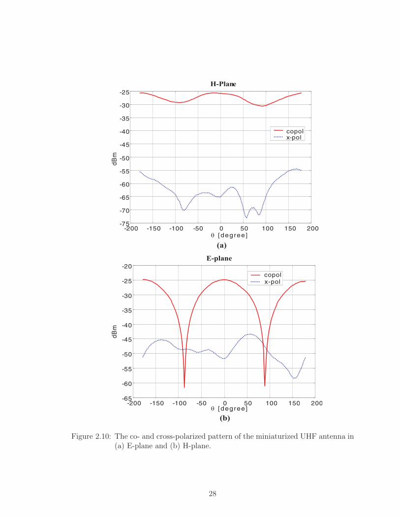
-200 -150 -100 -50 0 50 100 150 200 -75
-70
-65
-60
-55
-50
-45
-40
-35
-30
-25
θ [degree]
θ [degree]
dBm
dBm
H-Plane
copol x-pol
(a)
-200 -150 -100 -50 0 50 100 150 200 -65
-60
-55
-50
-45
-40
-35
-30
-25
-20
E-plane
x-pol
(b)
copol
Figure 2.10: The co- and cross-polarized pattern of the miniaturized UHF antenna in(a) E-plane and (b) H-plane.
28
shortens which renders a smaller antenna. As mentioned earlier, further antenna
miniaturization is accompanied by a reduction on the antenna bandwidth. Also
confining the electric currents on the ground plane into a smaller area results in
a higher ohmic loss, and consequently, a lower antenna efficiency.
2.5 Conclusion
A novel topology for designing electrically small resonant slot antenna is demon-
strated. A major size reduction was achieved by constructing a λg/4 resonant slot
rather than the traditional λg/2 antenna. This is accomplished by generating a virtual
open circuit at one end of the slot. Further miniaturization was achieved by bending
the slot into three pieces in order to use the area of the board more efficiently. The
antenna geometry occupies a very small area (0.014λ20) of a PC board with εr = 4.0
and a thickness of 3 mm. The antenna is very efficient and shows a gain as high as
that of a dipole antenna and a 1% bandwidth. It is also shown that if the antenna is
made on a small ground plane, its gain will be reduced and its radiation pattern will
change slightly.
29
CHAPTER 3
Miniaturization of Slot Antennas
3.1 Introduction
3.1.1 Background
The topic of small antennas has been a subject of interest for more than half
a century, but in recent years, it has attained significant attention because of an
exorbitant demand for mobile wireless communication systems. The need for antenna
miniaturization stems from the fact that most mobile platforms have a limited space
for all of the required antennas in ever increasing wireless systems. Compact antennas
are needed so that more antennas can be closely packed together without the risk of
mutual and parasitic coupling between them. For local area networks, there is an
emerging interest in making antennas small enough to ultimately fit on a single chip
with the rest of the receiving front-end. As part of a general trend in monolithic circuit
integration, using the area of substrate more efficiently is another strong motivation.
At low frequencies (HF-VHF), miniature antennas are in high demand, since the
antenna size often imposes a significant limitation on the overall size of a portable
wireless system.
30

3.1.2 Fundamental Limitations of Small Antennas
Earlier studies on small antennas focused on establishing a relationship between
the volume occupied by the antenna and its radiation characteristics and band-
width [1, 2, 3, 8, 9]. In these studies, a relation between the Quality Factor (Q)
of the antenna and the radius of the smallest fictitious spherical enclosure containing
the antenna was derived based on the spherical wave function expansion of the fields
radiated from the antenna. Each spherical mode was represented by an equivalent
circuit for which a quality factor (Qn) was calculated. Since the spherical eigenfunc-
tions are orthogonal, no energy could be coupled among modes. Therefore, the Q of
the antenna was expressed as a function of the Q of the individual modes. Finally, it
was shown that the quality factor of the lowest order mode is a lower bound for the
Q of a single resonant antenna [1]. A similar approach was adopted by Collin [10]
for cylindrical antennas using cylindrical wave functions to provide a tighter lower
limit on the Q of thin antennas with large aspect ratios. Results of these studies have
been summarized and referred to as the fundamental limitations of small antennas
[2]. However, in the above papers there are no discussions about procedures to design
miniaturized antennas.
In addition to high Q, another direct ramification of antenna miniaturization is
reduction in the antenna efficiency owing to the relatively high conduction and/or
polarization currents on the conductors or within the dielectric part of the antenna
structure. Furthermore, the matching network of a miniaturized antenna is usually
complex and lossy. Discussions regarding to the antenna efficiency and impedance
matching will be presented in more details in this chapter.
3.1.3 Approaches for Antenna Miniaturization
An example of miniaturized antennas is a meandered antenna where a half wave-
length dipole is made compact by meandering the wire [13]. A similar approach
31

can be applied to design a meander type slot antenna [14]. In order to increase the
efficiency of these antennas by reducing dissipation, the use of a high-temperature
superconductors (HTS) has been proposed [15, 16]. On the other hand, meandered
antennas are very hard to match to a 50 Ω line. This difficulty is due to the fact that
the radiation of almost in-phase electric currents flowing in opposite directions on
closely spaced wires tend to cancel each other in the far-field region. This cancella-
tion renders a considerable portion of opposing currents ineffective as far as radiation
efficiency is concerned and leads to a very low radiation resistance that might have
been increased using a two-strip meandered line [17]. Consequently, these antennas
are difficult to match, and yet, require a very low temperature of operation to control
material losses [18].
Another approach for antenna miniaturization, reported in the literature, is to use
very high dielectric constant materials in dielectric loaded antennas [19, 20]. Obvi-
ously, dielectric loading provides a size reduction factor on the order of√
εr for the
leaky dielectric and cavity resonator type antennas (e.g. microstrip patch antennas),
where εr is the relative permittivity of the dielectric material. This miniaturization
method, however, is less effective for terminated transmission line antennas, such
as slot or printed dipole antennas since these antennas see an effective permittivity
(εeff ), which is considerably less than εr. Although this method of miniaturization is
susceptible to surface wave excitation, it might be found beneficial, especially when
the electrical thickness of the substrate is small compared to the wavelength. It is
worth mentioning that this type of antenna miniaturization is not immune to the
aforementioned adverse effects such as high Q, low efficiency, and complexity in the
matching network.
There is another important methodology in antenna miniaturization; that is, mod-
ifying the antenna geometry. In Chapter 2, a new topology based on an S-shape
quarter wavelength resonant slot antenna was introduced using a short-circuit at one
32

end of the slot and an open-circuit at the other end. The open-circuit was realized by
a coiled quarter wavelength slot-line. Using this design, a very efficient miniaturized
antenna with dimensions of 0.12λ0 × 0.12λ0 on a substrate having εr = 4.0 was con-
structed and fed by a microstrip-line. The polarization of the radiated fields by this
antenna is frequency dependent, due to the fact that the radiating element is divided
into a three S-shape lines. It should also be noted that the size of this antenna cannot
be further miniaturized since its design is primarily based on the quarter-wavelength
structure.
Nevertheless, further miniaturization of slot antennas can be achieved by the vir-
tual enforcement of the required boundary condition at the end of a slot antenna,
whereby the area occupied by the resonant antenna can be reduced. To achieve the
required virtual Boundary Condition (BC), the two short-circuit at the end of the
standard resonant slot are replaced by some reactive BC, including inductive or ca-
pacitive loadings. The application of these loads is shown to reduce the size of the
resonant slot antenna for a given resonant frequency without imposing any stringent
condition on the impedance matching of the antenna.
In this chapter, a procedure for designing this class of miniaturized slot antennas
for any arbitrary size (relative to wavelength) is presented. As will be shown, in
order to locate the resonant frequency of this structure, the antenna is first fed by
a two-port microstrip line, and then, the location of the null in the insertion loss
(S21) is found and adjusted. The design procedure is based on an equivalent circuit
model for the antenna and its two-port feed structure. The corresponding equivalent
circuit parameters are extracted using a full-wave forward model in conjunction with
a Genetic Algorithm (GA) optimizer. These parameters are employed to find a proper
matching network so that a perfect match to a 50 Ω line is obtained.
Finally, a prototype slot antenna with approximate dimensions of 0.05λ0 × 0.05λ0
and a perfect impedance match is obtained, with a fairly high gain of −3 dBi, for a
33
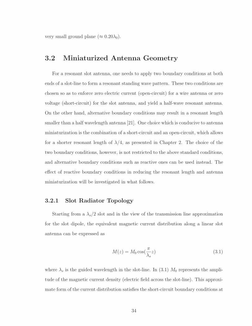
very small ground plane (≈ 0.20λ0).
3.2 Miniaturized Antenna Geometry
For a resonant slot antenna, one needs to apply two boundary conditions at both
ends of a slot-line to form a resonant standing wave pattern. These two conditions are
chosen so as to enforce zero electric current (open-circuit) for a wire antenna or zero
voltage (short-circuit) for the slot antenna, and yield a half-wave resonant antenna.
On the other hand, alternative boundary conditions may result in a resonant length
smaller than a half wavelength antenna [21]. One choice which is conducive to antenna
miniaturization is the combination of a short-circuit and an open-circuit, which allows
for a shorter resonant length of λ/4, as presented in Chapter 2. The choice of the
two boundary conditions, however, is not restricted to the above standard conditions,
and alternative boundary conditions such as reactive ones can be used instead. The
effect of reactive boundary conditions in reducing the resonant length and antenna
miniaturization will be investigated in what follows.
3.2.1 Slot Radiator Topology
Starting from a λs/2 slot and in the view of the transmission line approximation
for the slot dipole, the equivalent magnetic current distribution along a linear slot
antenna can be expressed as
M(z) = M0 cos(π
λs
z) (3.1)
where λs is the guided wavelength in the slot-line. In (3.1) M0 represents the ampli-
tude of the magnetic current density (electric field across the slot-line). This approxi-
mate form of the current distribution satisfies the short-circuit boundary conditions at
34
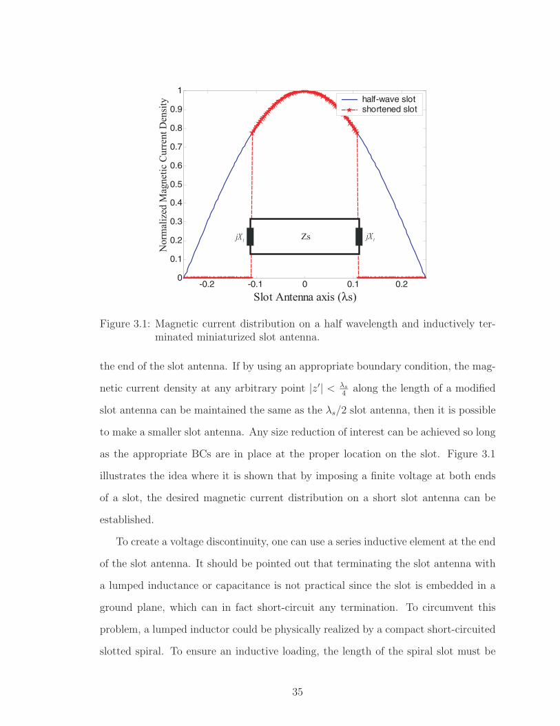
-0.2 -0.1 0 0.1 0.20
0.1
0.2
0.3
0.4
0.5
0.6
0.7
0.8
0.9
1half-wave slotshortened slot
Zs tjX
Slot Antenna axis (λs)
tjX
Nor
mal
ized
Mag
netic
Cur
rent
Den
sity
Figure 3.1: Magnetic current distribution on a half wavelength and inductively ter-minated miniaturized slot antenna.
the end of the slot antenna. If by using an appropriate boundary condition, the mag-
netic current density at any arbitrary point |z′| < λs
4along the length of a modified
slot antenna can be maintained the same as the λs/2 slot antenna, then it is possible
to make a smaller slot antenna. Any size reduction of interest can be achieved so long
as the appropriate BCs are in place at the proper location on the slot. Figure 3.1
illustrates the idea where it is shown that by imposing a finite voltage at both ends
of a slot, the desired magnetic current distribution on a short slot antenna can be
established.
To create a voltage discontinuity, one can use a series inductive element at the end
of the slot antenna. It should be pointed out that terminating the slot antenna with
a lumped inductance or capacitance is not practical since the slot is embedded in a
ground plane, which can in fact short-circuit any termination. To circumvent this
problem, a lumped inductor could be physically realized by a compact short-circuited
slotted spiral. To ensure an inductive loading, the length of the spiral slot must be
35
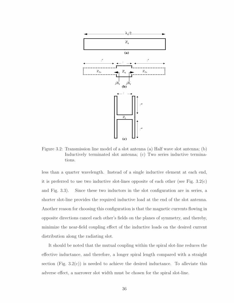
λ /2s
Zs Z1sZ1s
Zs
jXt jXt
′′
(a)
(b)
Zs
″
″
(c)
Figure 3.2: Transmission line model of a slot antenna (a) Half wave slot antenna; (b)Inductively terminated slot antenna; (c) Two series inductive termina-tions.
less than a quarter wavelength. Instead of a single inductive element at each end,
it is preferred to use two inductive slot-lines opposite of each other (see Fig. 3.2(c)
and Fig. 3.3). Since these two inductors in the slot configuration are in series, a
shorter slot-line provides the required inductive load at the end of the slot antenna.
Another reason for choosing this configuration is that the magnetic currents flowing in
opposite directions cancel each other’s fields on the planes of symmetry, and thereby,
minimize the near-field coupling effect of the inductive loads on the desired current
distribution along the radiating slot.
It should be noted that the mutual coupling within the spiral slot-line reduces the
effective inductance, and therefore, a longer spiral length compared with a straight
section (Fig. 3.2(c)) is needed to achieve the desired inductance. To alleviate this
adverse effect, a narrower slot width must be chosen for the spiral slot-line.
36
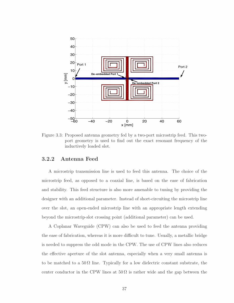
−60 −40 −20 0 20 40 60−50
−40
−30
−20
−10
0
10
20
30
40
50
x [mm]
y [m
m]
Port 2 Port 1
De−embedded Port 1
De−embedded Port 2
Figure 3.3: Proposed antenna geometry fed by a two-port microstrip feed. This two-port geometry is used to find out the exact resonant frequency of theinductively loaded slot.
3.2.2 Antenna Feed
A microstrip transmission line is used to feed this antenna. The choice of the
microstrip feed, as opposed to a coaxial line, is based on the ease of fabrication
and stability. This feed structure is also more amenable to tuning by providing the
designer with an additional parameter. Instead of short-circuiting the microstrip line
over the slot, an open-ended microstrip line with an appropriate length extending
beyond the microstrip-slot crossing point (additional parameter) can be used.
A Coplanar Waveguide (CPW) can also be used to feed the antenna providing
the ease of fabrication, whereas it is more difficult to tune. Usually, a metallic bridge
is needed to suppress the odd mode in the CPW. The use of CPW lines also reduces
the effective aperture of the slot antenna, especially when a very small antenna is
to be matched to a 50 Ω line. Typically for a low dielectric constant substrate, the
center conductor in the CPW lines at 50 Ω is rather wide and the gap between the
37
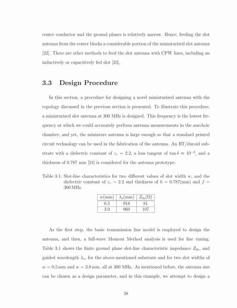
center conductor and the ground planes is relatively narrow. Hence, feeding the slot
antenna from the center blocks a considerable portion of the miniaturized slot antenna
[22]. There are other methods to feed the slot antenna with CPW lines, including an
inductively or capacitively fed slot [23].
3.3 Design Procedure
In this section, a procedure for designing a novel miniaturized antenna with the
topology discussed in the previous section is presented. To illustrate this procedure,
a miniaturized slot antenna at 300 MHz is designed. This frequency is the lowest fre-
quency at which we could accurately perform antenna measurements in the anechoic
chamber, and yet, the miniature antenna is large enough so that a standard printed
circuit technology can be used in the fabrication of the antenna. An RT/duroid sub-
strate with a dielectric constant of εr = 2.2, a loss tangent of tan δ ≈ 10−3, and a
thickness of 0.787 mm [24] is considered for the antenna prototype.
Table 3.1: Slot-line characteristics for two different values of slot width w, and thedielectric constant of εr = 2.2 and thickness of h = 0.787(mm) and f =300 MHz.
w(mm) λs(mm) Z0s(Ω)
0.5 918 813.0 960 107
As the first step, the basic transmission line model is employed to design the
antenna, and then, a full-wave Moment Method analysis is used for fine tuning.
Table 3.1 shows the finite ground plane slot-line characteristic impedance Z0s, and
guided wavelength λs, for the above-mentioned substrate and for two slot widths of
w = 0.5 mm and w = 3.0 mm, all at 300 MHz. As mentioned before, the antenna size
can be chosen as a design parameter, and in this example, we attempt to design a
38
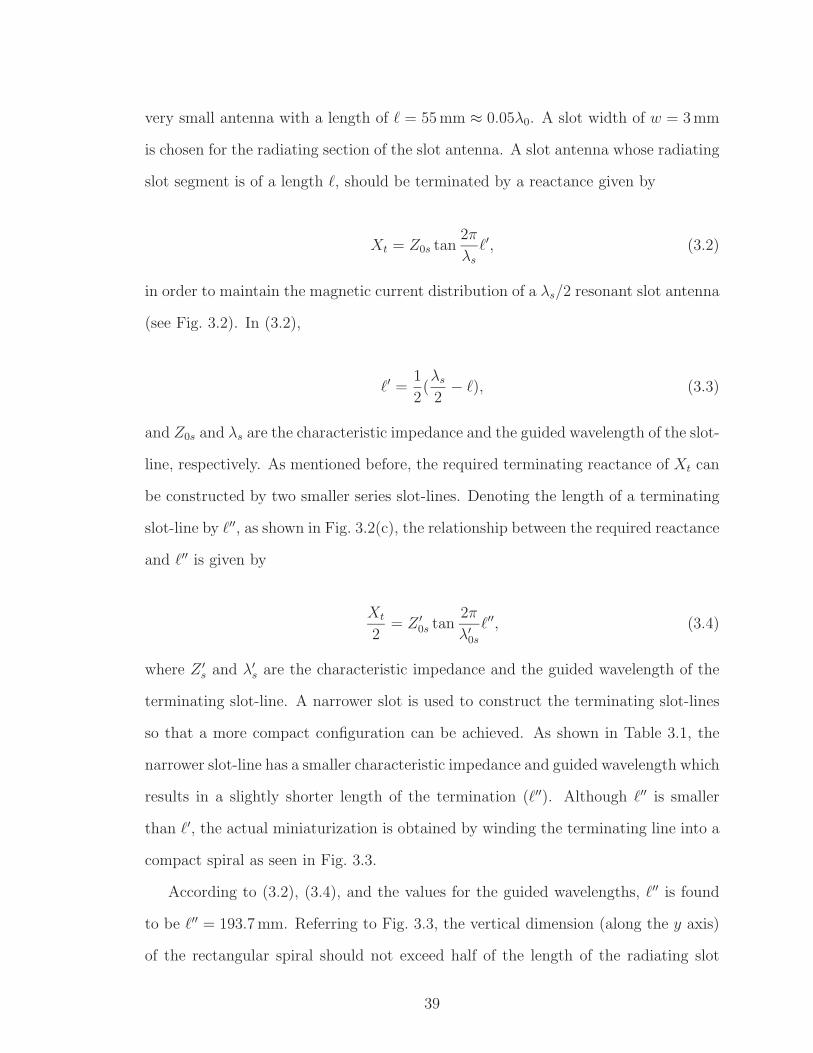
very small antenna with a length of = 55 mm ≈ 0.05λ0. A slot width of w = 3 mm
is chosen for the radiating section of the slot antenna. A slot antenna whose radiating
slot segment is of a length , should be terminated by a reactance given by
Xt = Z0s tan2π
λs
′, (3.2)
in order to maintain the magnetic current distribution of a λs/2 resonant slot antenna
(see Fig. 3.2). In (3.2),
′ =1
2(λs
2− ), (3.3)
and Z0s and λs are the characteristic impedance and the guided wavelength of the slot-
line, respectively. As mentioned before, the required terminating reactance of Xt can
be constructed by two smaller series slot-lines. Denoting the length of a terminating
slot-line by ′′, as shown in Fig. 3.2(c), the relationship between the required reactance
and ′′ is given by
Xt
2= Z ′
0s tan2π
λ′0s
′′, (3.4)
where Z ′s and λ′
s are the characteristic impedance and the guided wavelength of the
terminating slot-line. A narrower slot is used to construct the terminating slot-lines
so that a more compact configuration can be achieved. As shown in Table 3.1, the
narrower slot-line has a smaller characteristic impedance and guided wavelength which
results in a slightly shorter length of the termination (′′). Although ′′ is smaller
than ′, the actual miniaturization is obtained by winding the terminating line into a
compact spiral as seen in Fig. 3.3.
According to (3.2), (3.4), and the values for the guided wavelengths, ′′ is found
to be ′′ = 193.7 mm. Referring to Fig. 3.3, the vertical dimension (along the y axis)
of the rectangular spiral should not exceed half of the length of the radiating slot
39

segment (). This constraint on the inductive rectangular spiral is imposed so that
the entire antenna structure can fit into a square area of 55 mm × 55 mm, which is
about 0.05λ0×0.05λ0. Since the dielectric constant and the thickness of the substrate
chosen for this design are very low (εr = 2.2), the guided wavelength (λs = 96 cm)
is not very much different from that of the free space (λ0 = 100 cm). Thus, the
miniaturization is mainly achieved by the proper choice of the antenna topology. It is
worth mentioning that further size reduction can be obtained once a substrate with
higher permittivity is used.
3.4 Full-Wave Simulation and Tuning
In the previous section, the transmission line model was employed for design-
ing the proposed miniature antenna. Although this model is not very accurate, it
provides the intuition necessary for designing the novel topology. The transmission
line model ignores the coupling between the adjacent slot-lines and the microstrip
to slot transition. For calculation of the input impedance, and exact determination
of the length of different slot-line segments, a full-wave simulation tool is required.
IE3D, a commercially available Moment Method code, is used for required numerical
simulations [25].
Figure 3.3 shows the proposed antenna geometry fed by a two-port 50 Ω microstrip
line. The two-port structure is constructed to study the resonant frequency of the
antenna as well as the transition between the microstrip-line and slot antenna. The
microstrip line is extended well beyond the slot transition point so that the port ter-
minals do not couple to the slot antenna. The radiating slot length is chosen to be
= 55 mm, and the length of the rectangular spirals are tuned such that the antenna
resonates at 300 MHz. The resonance at the desired frequency is indicated by a deep
null in the frequency response of S21. The simulated S-parameters of this two-port
40
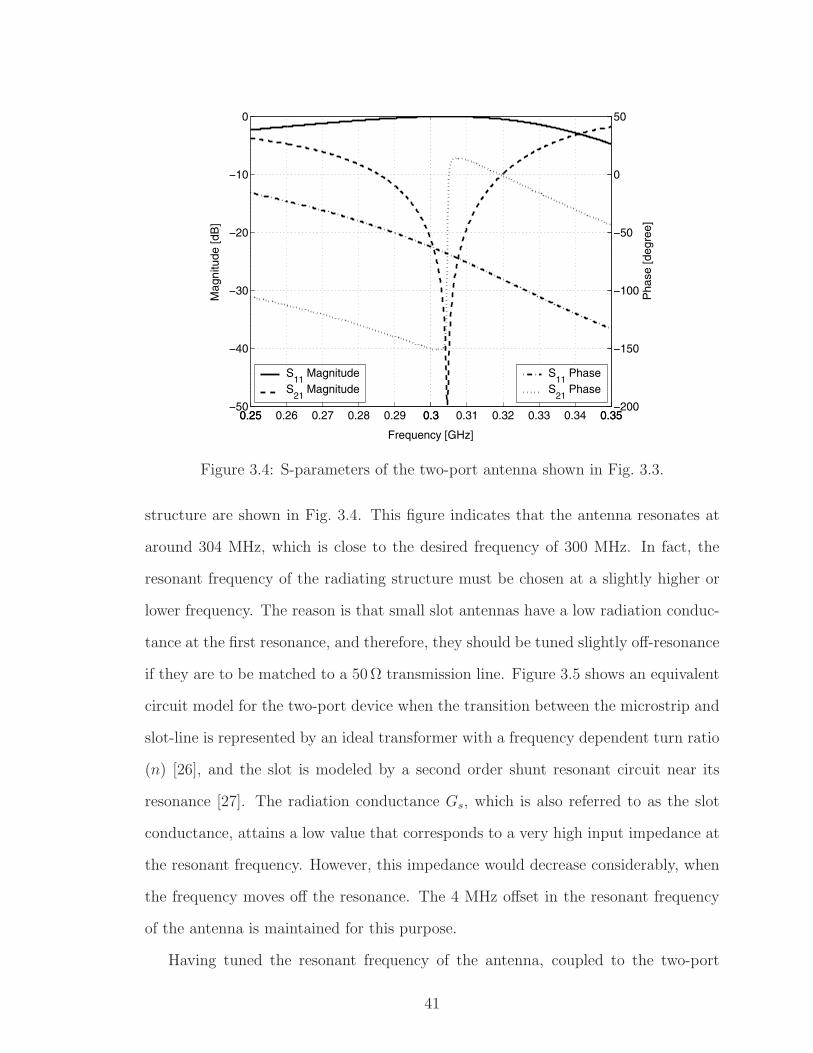
0.25 0.3 0.35−50
−40
−30
−20
−10
0
Mag
nitu
de [d
B]
Frequency [GHz]
S11
MagnitudeS
21 Magnitude
0.25 0.26 0.27 0.28 0.29 0.3 0.31 0.32 0.33 0.34 0.35−200
−150
−100
−50
0
50
Pha
se [d
egre
e]
S11
PhaseS
21 Phase
Figure 3.4: S-parameters of the two-port antenna shown in Fig. 3.3.
structure are shown in Fig. 3.4. This figure indicates that the antenna resonates at
around 304 MHz, which is close to the desired frequency of 300 MHz. In fact, the
resonant frequency of the radiating structure must be chosen at a slightly higher or
lower frequency. The reason is that small slot antennas have a low radiation conduc-
tance at the first resonance, and therefore, they should be tuned slightly off-resonance
if they are to be matched to a 50 Ω transmission line. Figure 3.5 shows an equivalent
circuit model for the two-port device when the transition between the microstrip and
slot-line is represented by an ideal transformer with a frequency dependent turn ratio
(n) [26], and the slot is modeled by a second order shunt resonant circuit near its
resonance [27]. The radiation conductance Gs, which is also referred to as the slot
conductance, attains a low value that corresponds to a very high input impedance at
the resonant frequency. However, this impedance would decrease considerably, when
the frequency moves off the resonance. The 4 MHz offset in the resonant frequency
of the antenna is maintained for this purpose.
Having tuned the resonant frequency of the antenna, coupled to the two-port
41
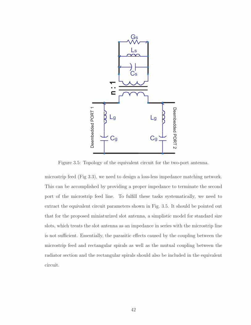
Lg
Gs
Lg
CgCg
Cs
Ls
n : 1
Dee
mbe
dded
PO
RT
1 Deem
bedded POR
T 2
Figure 3.5: Topology of the equivalent circuit for the two-port antenna.
microstrip feed (Fig 3.3), we need to design a loss-less impedance matching network.
This can be accomplished by providing a proper impedance to terminate the second
port of the microstrip feed line. To fulfill these tasks systematically, we need to
extract the equivalent circuit parameters shown in Fig. 3.5. It should be pointed out
that for the proposed miniaturized slot antenna, a simplistic model for standard size
slots, which treats the slot antenna as an impedance in series with the microstrip line
is not sufficient. Essentially, the parasitic effects caused by the coupling between the
microstrip feed and rectangular spirals as well as the mutual coupling between the
radiator section and the rectangular spirals should also be included in the equivalent
circuit.
42
3.4.1 Equivalent-Circuit Model
In this section, an equivalent circuit model for the proposed antenna is developed.
This model is capable of predicting the slot radiation conductance and the antenna
input impedance near resonance. This approach provides very helpful insight as to
how this antenna and its feed network operate. As mentioned before, this model is
also needed to find a proper matching network for the antenna.
Near resonant frequencies, the slot antenna can be modeled by a simple second
order RLC circuit. Since the voltage across the slot excites the slot antenna at the
feed point, it is appropriate to use the shunt resonant model for the radiating slot as
shown in Fig. 3.5. The coupling between the microstrip and the slot is modeled by a
series ideal transformer with a turn ratio n.
To model the feeding mechanism right at the cross junction of the microstrip
and slot, it is necessary to deembed the effect of the microstrip lines between the
terminals and the crossing points. There are different deembedding schemes reported
in the literature [28, 29]. The advantage of proper deembedding as opposed to the
mere shifting of the reference planes by the corresponding phase factor is to exclude
the effect of radiation and other parasitic effects of the line.
To model the parasitic coupling of the microstrip line and the slot (coupling of
radiated field from the microstrip line and slot), two additional parasitic parameters,
namely, Lg and Cg are included in the model. The use of shunt parasitic parameters
has previously been suggested to model the effects of fields as perturbed by a wide
slot [30]. Figure 3.6 shows the deembedded Y-parameters of the two-port microstrip-
fed slot antenna where the location of deembedded ports are shown in Fig. 3.3. Note
that these two ports are now defined at the microstrip-slot junction. According to
the lumped element model of Fig. 3.5, the Y-parameters are given by:
Y11 =−j
Lgω − 1Cgω
+1
n2[Gs + j(Csω − 1
Lsω)] (3.5)
43
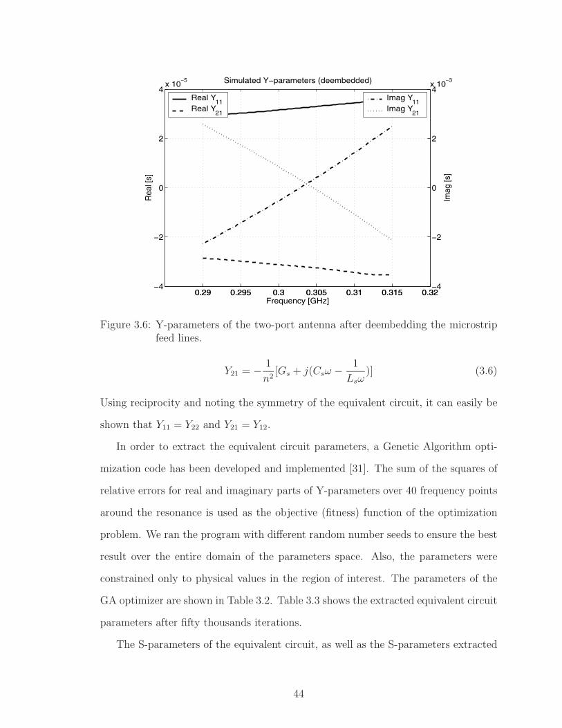
0.29 0.295 0.3 0.305 0.31 0.315 0.32−4
−2
0
2
4x 10
−5
Rea
l [s]
Frequency [GHz]
Simulated Y−parameters (deembedded)
Real Y11
Real Y21
0.29 0.295 0.3 0.305 0.31 0.315 0.32−4
−2
0
2
4x 10
−3
Imag
[s]
Imag Y11
Imag Y
21
Figure 3.6: Y-parameters of the two-port antenna after deembedding the microstripfeed lines.
Y21 = − 1
n2[Gs + j(Csω − 1
Lsω)] (3.6)
Using reciprocity and noting the symmetry of the equivalent circuit, it can easily be
shown that Y11 = Y22 and Y21 = Y12.
In order to extract the equivalent circuit parameters, a Genetic Algorithm opti-
mization code has been developed and implemented [31]. The sum of the squares of
relative errors for real and imaginary parts of Y-parameters over 40 frequency points
around the resonance is used as the objective (fitness) function of the optimization
problem. We ran the program with different random number seeds to ensure the best
result over the entire domain of the parameters space. Also, the parameters were
constrained only to physical values in the region of interest. The parameters of the
GA optimizer are shown in Table 3.2. Table 3.3 shows the extracted equivalent circuit
parameters after fifty thousands iterations.
The S-parameters of the equivalent circuit, as well as the S-parameters extracted
44

Table 3.2: The parameters of the Genetic Algorithm optimizer.
Population Size 300Number of Iteration 50,000Chromosome Length 128
PCrossover 0.55PMutation 0.005
Table 3.3: The equivalent circuit parameters of the microstrip fed slot antenna.
Turn Ratio (n) 0.948007Rs(Ω) 33979
Ls(µH) 0.0207Cs(pF ) 13.1744Lg(µH) 0.49997Cg(pF ) 0.125
from the full-wave analysis, are shown in Fig. 3.7. Excellent agreement is observed
between the full-wave results and those of the equivalent circuit.
3.4.2 Antenna Matching
Having found the equivalent circuit parameters, the antenna’s matching network
can readily be designed. For matching networks, especially when efficiency is the
main concern, loss-less terminations are usually desired. Therefore, we seek a purely
reactive admittance to terminate the feed line, which in fact is the load for the second
port of the two-port equivalent circuit model. The explicit expression for a termina-
tion admittance (Yt) to be placed at the second terminal of the two-port model in
order to match the impedance of the antenna is given by:
Yt = −Y11 +Y 2
12
Y11 − Y0
. (3.7)
Fig. 3.8 shows the spectral behavior of Yt for a standard 50 Ω line (Y0 = 0.02).
45
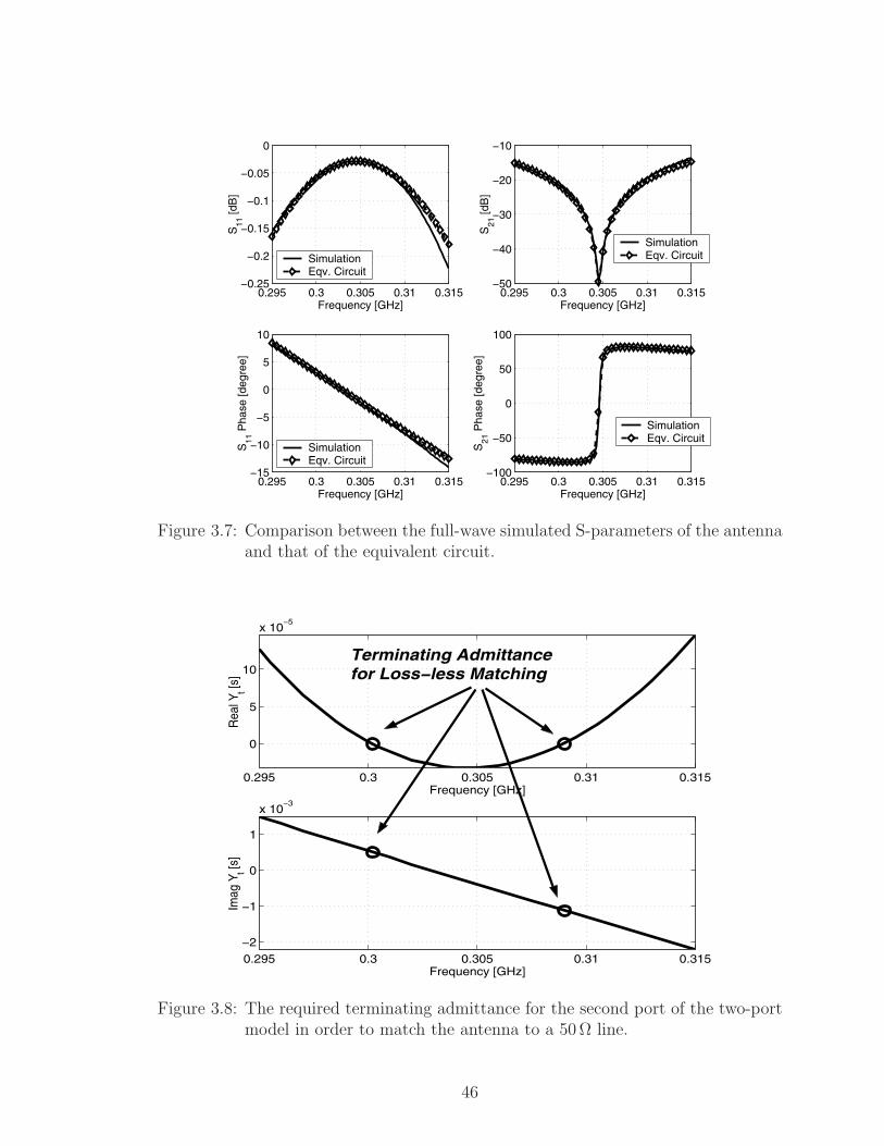
0.295 0.3 0.305 0.31 0.315−0.25
−0.2
−0.15
−0.1
−0.05
0
Frequency [GHz]
S11
[dB
]
SimulationEqv. Circuit
0.295 0.3 0.305 0.31 0.315−50
−40
−30
−20
−10
Frequency [GHz]
S21
[dB
]
SimulationEqv. Circuit
0.295 0.3 0.305 0.31 0.315−15
−10
−5
0
5
10
Frequency [GHz]
S11
Pha
se [d
egre
e]
SimulationEqv. Circuit
0.295 0.3 0.305 0.31 0.315−100
−50
0
50
100
Frequency [GHz]S
21 P
hase
[deg
ree]
SimulationEqv. Circuit
Figure 3.7: Comparison between the full-wave simulated S-parameters of the antennaand that of the equivalent circuit.
0.295 0.3 0.305 0.31 0.315
0
5
10
x 10−5
Frequency [GHz]
Rea
l Yt [s
]
0.295 0.3 0.305 0.31 0.315−2
−1
0
1
x 10−3
Frequency [GHz]
Imag
Yt [s
]
Terminating Admittancefor Loss−less Matching
Figure 3.8: The required terminating admittance for the second port of the two-portmodel in order to match the antenna to a 50 Ω line.
46
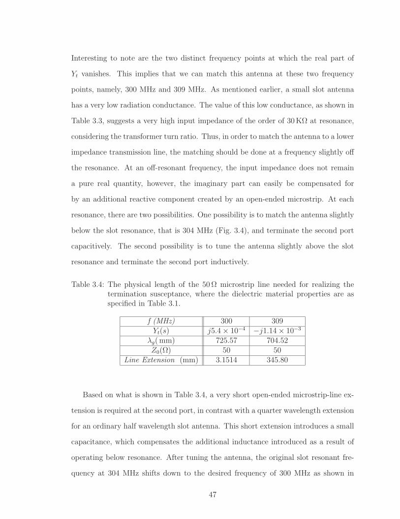
Interesting to note are the two distinct frequency points at which the real part of
Yt vanishes. This implies that we can match this antenna at these two frequency
points, namely, 300 MHz and 309 MHz. As mentioned earlier, a small slot antenna
has a very low radiation conductance. The value of this low conductance, as shown in
Table 3.3, suggests a very high input impedance of the order of 30 KΩ at resonance,
considering the transformer turn ratio. Thus, in order to match the antenna to a lower
impedance transmission line, the matching should be done at a frequency slightly off
the resonance. At an off-resonant frequency, the input impedance does not remain
a pure real quantity, however, the imaginary part can easily be compensated for
by an additional reactive component created by an open-ended microstrip. At each
resonance, there are two possibilities. One possibility is to match the antenna slightly
below the slot resonance, that is 304 MHz (Fig. 3.4), and terminate the second port
capacitively. The second possibility is to tune the antenna slightly above the slot
resonance and terminate the second port inductively.
Table 3.4: The physical length of the 50 Ω microstrip line needed for realizing thetermination susceptance, where the dielectric material properties are asspecified in Table 3.1.
f (MHz) 300 309Yt(s) j5.4 × 10−4 −j1.14 × 10−3
λg( mm) 725.57 704.52Z0(Ω) 50 50
Line Extension (mm) 3.1514 345.80
Based on what is shown in Table 3.4, a very short open-ended microstrip-line ex-
tension is required at the second port, in contrast with a quarter wavelength extension
for an ordinary half wavelength slot antenna. This short extension introduces a small
capacitance, which compensates the additional inductance introduced as a result of
operating below resonance. After tuning the antenna, the original slot resonant fre-
quency at 304 MHz shifts down to the desired frequency of 300 MHz as shown in
47
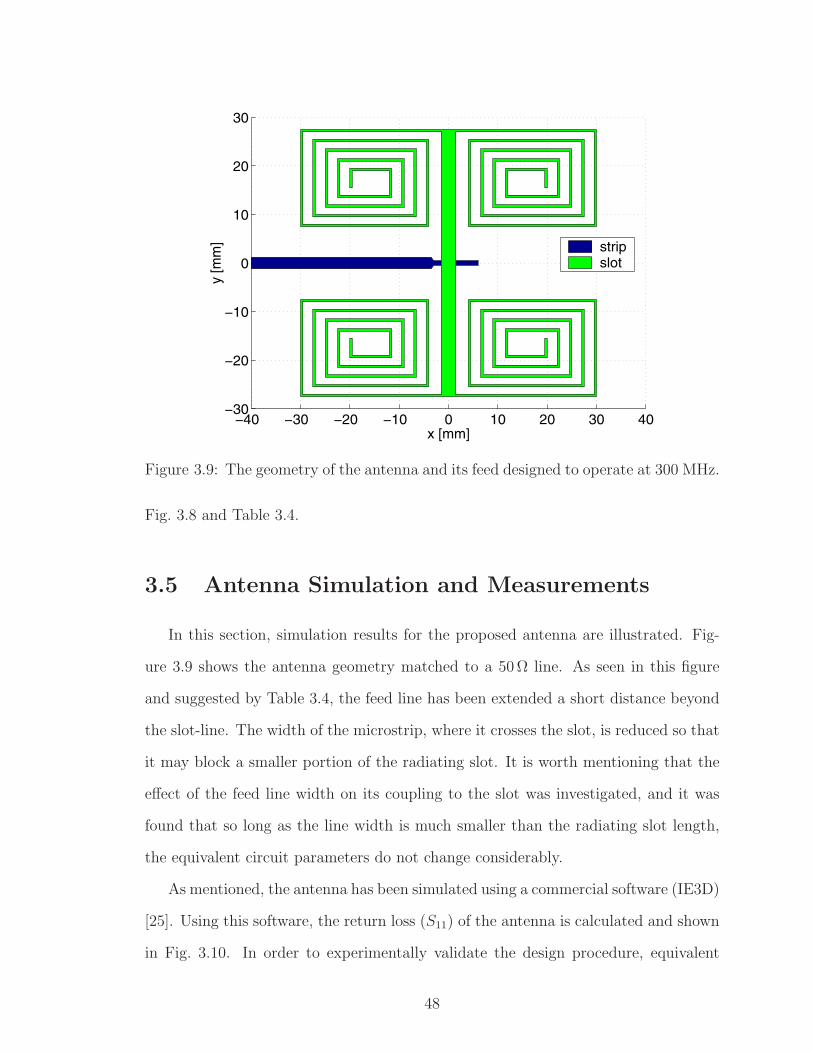
−40 −30 −20 −10 0 10 20 30 40−30
−20
−10
0
10
20
30
y [m
m]
x [mm]
stripslot
Figure 3.9: The geometry of the antenna and its feed designed to operate at 300 MHz.
Fig. 3.8 and Table 3.4.
3.5 Antenna Simulation and Measurements
In this section, simulation results for the proposed antenna are illustrated. Fig-
ure 3.9 shows the antenna geometry matched to a 50 Ω line. As seen in this figure
and suggested by Table 3.4, the feed line has been extended a short distance beyond
the slot-line. The width of the microstrip, where it crosses the slot, is reduced so that
it may block a smaller portion of the radiating slot. It is worth mentioning that the
effect of the feed line width on its coupling to the slot was investigated, and it was
found that so long as the line width is much smaller than the radiating slot length,
the equivalent circuit parameters do not change considerably.
As mentioned, the antenna has been simulated using a commercial software (IE3D)
[25]. Using this software, the return loss (S11) of the antenna is calculated and shown
in Fig. 3.10. In order to experimentally validate the design procedure, equivalent
48
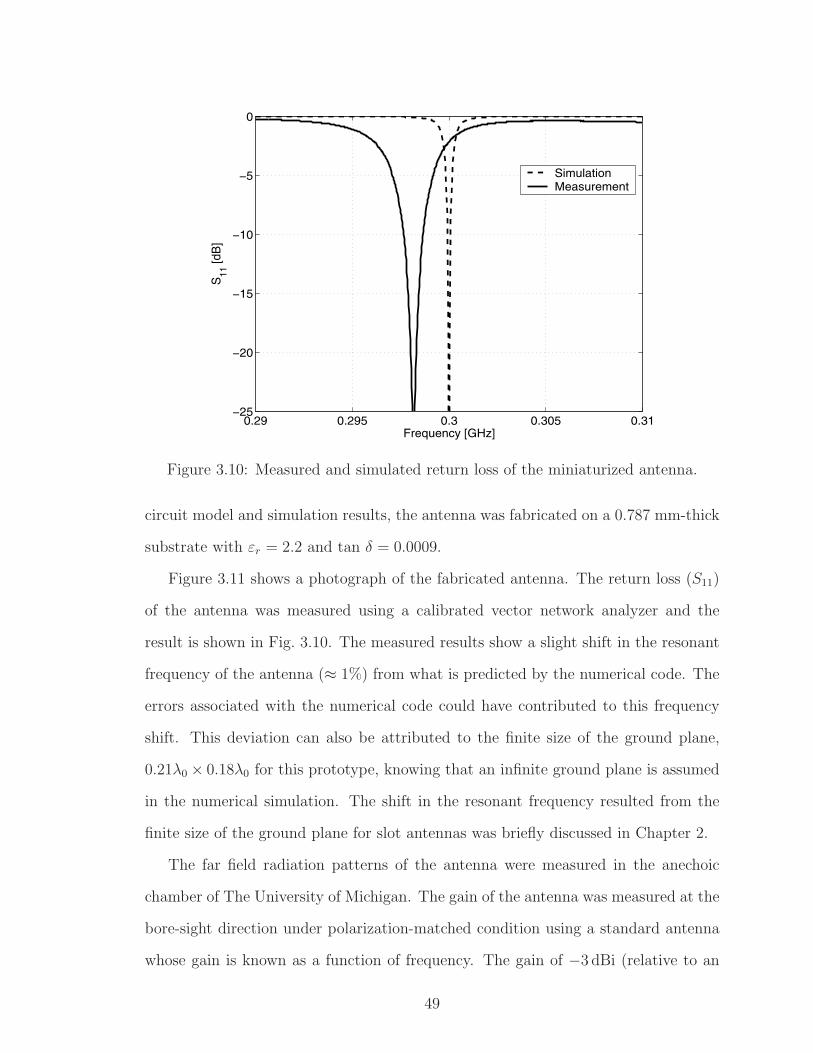
0.29 0.295 0.3 0.305 0.31−25
−20
−15
−10
−5
0
Frequency [GHz]
S11
[dB
]
SimulationMeasurement
Figure 3.10: Measured and simulated return loss of the miniaturized antenna.
circuit model and simulation results, the antenna was fabricated on a 0.787 mm-thick
substrate with εr = 2.2 and tan δ = 0.0009.
Figure 3.11 shows a photograph of the fabricated antenna. The return loss (S11)
of the antenna was measured using a calibrated vector network analyzer and the
result is shown in Fig. 3.10. The measured results show a slight shift in the resonant
frequency of the antenna (≈ 1%) from what is predicted by the numerical code. The
errors associated with the numerical code could have contributed to this frequency
shift. This deviation can also be attributed to the finite size of the ground plane,
0.21λ0 × 0.18λ0 for this prototype, knowing that an infinite ground plane is assumed
in the numerical simulation. The shift in the resonant frequency resulted from the
finite size of the ground plane for slot antennas was briefly discussed in Chapter 2.
The far field radiation patterns of the antenna were measured in the anechoic
chamber of The University of Michigan. The gain of the antenna was measured at the
bore-sight direction under polarization-matched condition using a standard antenna
whose gain is known as a function of frequency. The gain of −3 dBi (relative to an
49
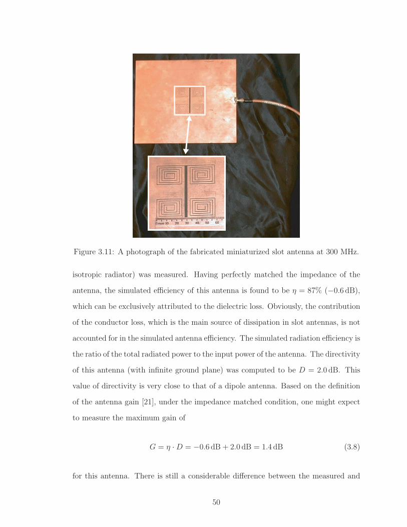
Figure 3.11: A photograph of the fabricated miniaturized slot antenna at 300 MHz.
isotropic radiator) was measured. Having perfectly matched the impedance of the
antenna, the simulated efficiency of this antenna is found to be η = 87% (−0.6 dB),
which can be exclusively attributed to the dielectric loss. Obviously, the contribution
of the conductor loss, which is the main source of dissipation in slot antennas, is not
accounted for in the simulated antenna efficiency. The simulated radiation efficiency is
the ratio of the total radiated power to the input power of the antenna. The directivity
of this antenna (with infinite ground plane) was computed to be D = 2.0 dB. This
value of directivity is very close to that of a dipole antenna. Based on the definition
of the antenna gain [21], under the impedance matched condition, one might expect
to measure the maximum gain of
G = η · D = −0.6 dB + 2.0 dB = 1.4 dB (3.8)
for this antenna. There is still a considerable difference between the measured and
50
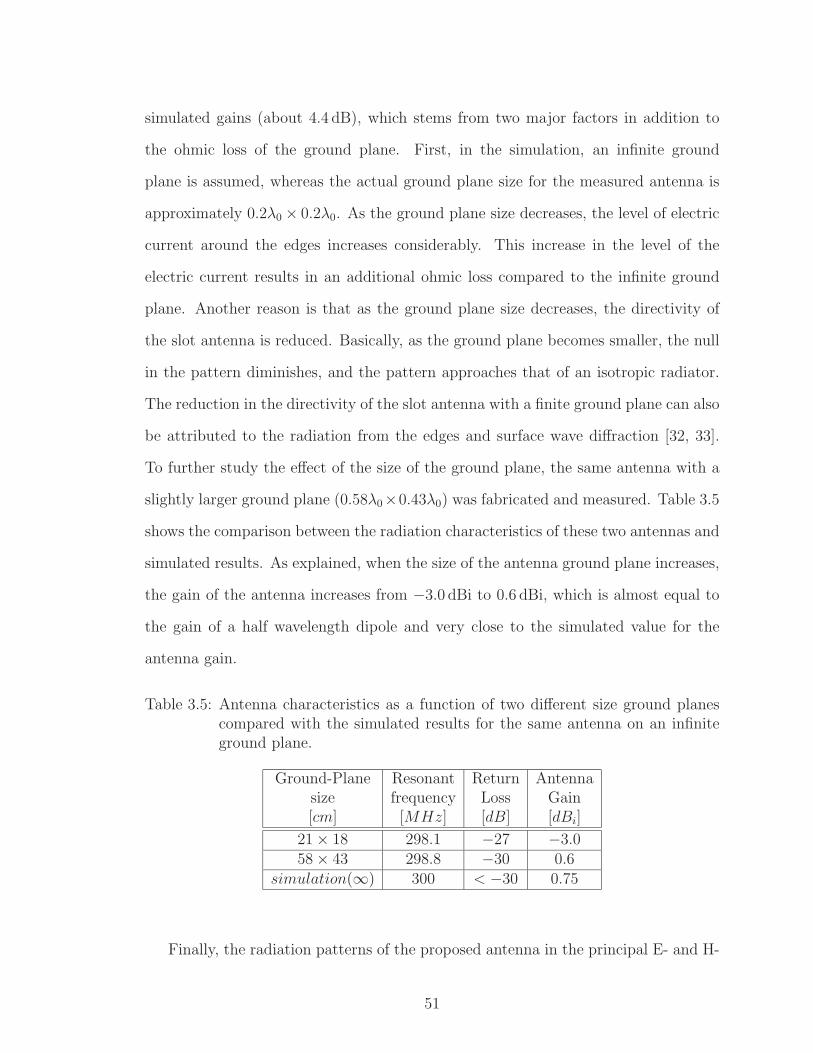
simulated gains (about 4.4 dB), which stems from two major factors in addition to
the ohmic loss of the ground plane. First, in the simulation, an infinite ground
plane is assumed, whereas the actual ground plane size for the measured antenna is
approximately 0.2λ0 × 0.2λ0. As the ground plane size decreases, the level of electric
current around the edges increases considerably. This increase in the level of the
electric current results in an additional ohmic loss compared to the infinite ground
plane. Another reason is that as the ground plane size decreases, the directivity of
the slot antenna is reduced. Basically, as the ground plane becomes smaller, the null
in the pattern diminishes, and the pattern approaches that of an isotropic radiator.
The reduction in the directivity of the slot antenna with a finite ground plane can also
be attributed to the radiation from the edges and surface wave diffraction [32, 33].
To further study the effect of the size of the ground plane, the same antenna with a
slightly larger ground plane (0.58λ0×0.43λ0) was fabricated and measured. Table 3.5
shows the comparison between the radiation characteristics of these two antennas and
simulated results. As explained, when the size of the antenna ground plane increases,
the gain of the antenna increases from −3.0 dBi to 0.6 dBi, which is almost equal to
the gain of a half wavelength dipole and very close to the simulated value for the
antenna gain.
Table 3.5: Antenna characteristics as a function of two different size ground planescompared with the simulated results for the same antenna on an infiniteground plane.
Ground-Plane Resonant Return Antennasize frequency Loss Gain[cm] [MHz] [dB] [dBi]
21 × 18 298.1 −27 −3.058 × 43 298.8 −30 0.6
simulation(∞) 300 < −30 0.75
Finally, the radiation patterns of the proposed antenna in the principal E- and H-
51
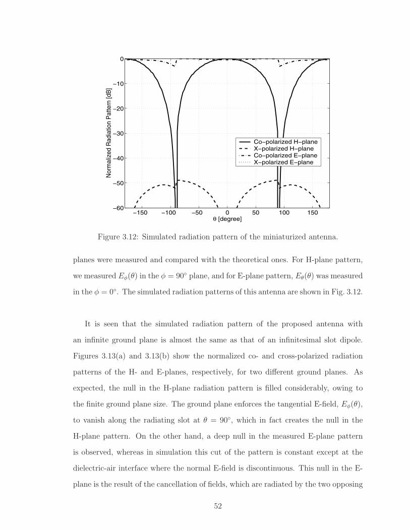
−150 −100 −50 0 50 100 150−60
−50
−40
−30
−20
−10
0
θ [degree]
Nor
mal
ized
Rad
iatio
n P
atte
rn [d
B]
Co−polarized H−planeX−polarized H−planeCo−polarized E−planeX−polarized E−plane
Figure 3.12: Simulated radiation pattern of the miniaturized antenna.
planes were measured and compared with the theoretical ones. For H-plane pattern,
we measured Eφ(θ) in the φ = 90 plane, and for E-plane pattern, Eθ(θ) was measured
in the φ = 0. The simulated radiation patterns of this antenna are shown in Fig. 3.12.
It is seen that the simulated radiation pattern of the proposed antenna with
an infinite ground plane is almost the same as that of an infinitesimal slot dipole.
Figures 3.13(a) and 3.13(b) show the normalized co- and cross-polarized radiation
patterns of the H- and E-planes, respectively, for two different ground planes. As
expected, the null in the H-plane radiation pattern is filled considerably, owing to
the finite ground plane size. The ground plane enforces the tangential E-field, Eφ(θ),
to vanish along the radiating slot at θ = 90, which in fact creates the null in the
H-plane pattern. On the other hand, a deep null in the measured E-plane pattern
is observed, whereas in simulation this cut of the pattern is constant except at the
dielectric-air interface where the normal E-field is discontinuous. This null in the E-
plane is the result of the cancellation of fields, which are radiated by the two opposing
52
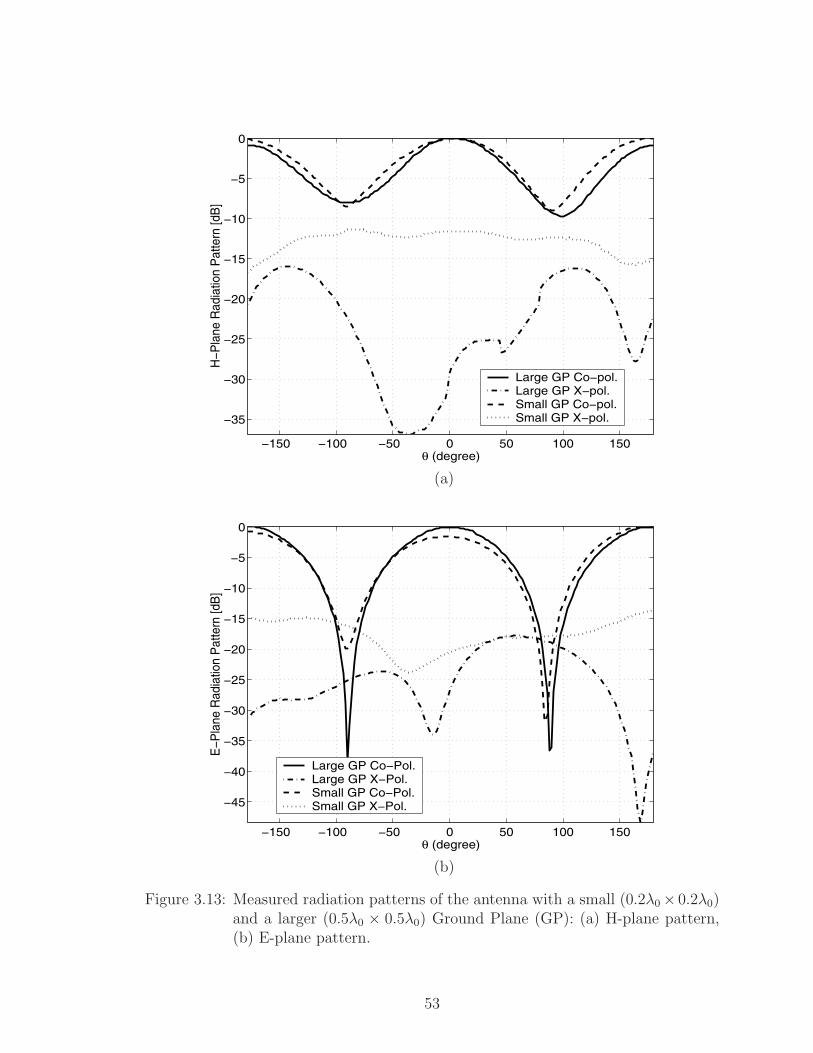
−150 −100 −50 0 50 100 150
−35
−30
−25
−20
−15
−10
−5
0
θ (degree)
H−P
lane
Rad
iatio
n P
atte
rn [d
B]
Large GP Co−pol.Large GP X−pol.Small GP Co−pol.Small GP X−pol.
(a)
−150 −100 −50 0 50 100 150
−45
−40
−35
−30
−25
−20
−15
−10
−5
0
θ (degree)
E−P
lane
Rad
iatio
n P
atte
rn [d
B]
Large GP Co−Pol.Large GP X−Pol.Small GP Co−Pol.Small GP X−Pol.
(b)
Figure 3.13: Measured radiation patterns of the antenna with a small (0.2λ0 × 0.2λ0)and a larger (0.5λ0 × 0.5λ0) Ground Plane (GP): (a) H-plane pattern,(b) E-plane pattern.
53
magnetic currents. The equivalent magnetic currents, flowing in the upper and lower
side of the ground plane, are in opposite directions and consequently, their radiations
in the point of symmetry at the E-plane cancel each other. However, in the case of
an infinite ground plane, the upper and lower half-spaces are isolated and therefore,
the E-plane radiation pattern remains constant. Appendix A will further delineate
the effect of the finite ground plane on the radiation pattern of slot antennas.
Moreover, an increase in the measured cross-polarized component is observed as
compared with the simulation results. Although it may seem that there is a consider-
able cross polarization radiation due to the presence of spiral slots at the terminations,
there is no such a component in the principal planes as well as the φ = ±45 planes
since the geometry is symmetric with respect to those planes. The cross polarization
appeared in these measurements is mainly caused by radiation from the edges as well
as the feed cable. The radiated field of the antenna is always capable of inducing
currents on the feeding cable, especially when the ground plane size is very small
compared to the wavelength. Then, the induced currents re-radiate and give rise to
the cross polarization. Moreover, the contribution of the anechoic chamber, giving
rise to the cross-polarized component at the low frequency of 300 MHz, is also another
factor. Nevertheless, both of the above-mentioned sources for the cross-polarization
can be eliminated by increasing the size of the ground plane.
3.6 Conformability to Curved Platforms
Interest in conformal and low profile antennas is in response to mobility, space
and airborne requirements. To meet these requirements all at once, the application of
slot antennas is a prudent choice. A slotted structure can be mounted on the body of
mobile platforms such as airplanes, cars, etc. A slot antenna topology is also desired
since it is invisible and does not change the profile of the mobile platform. Knowing
54
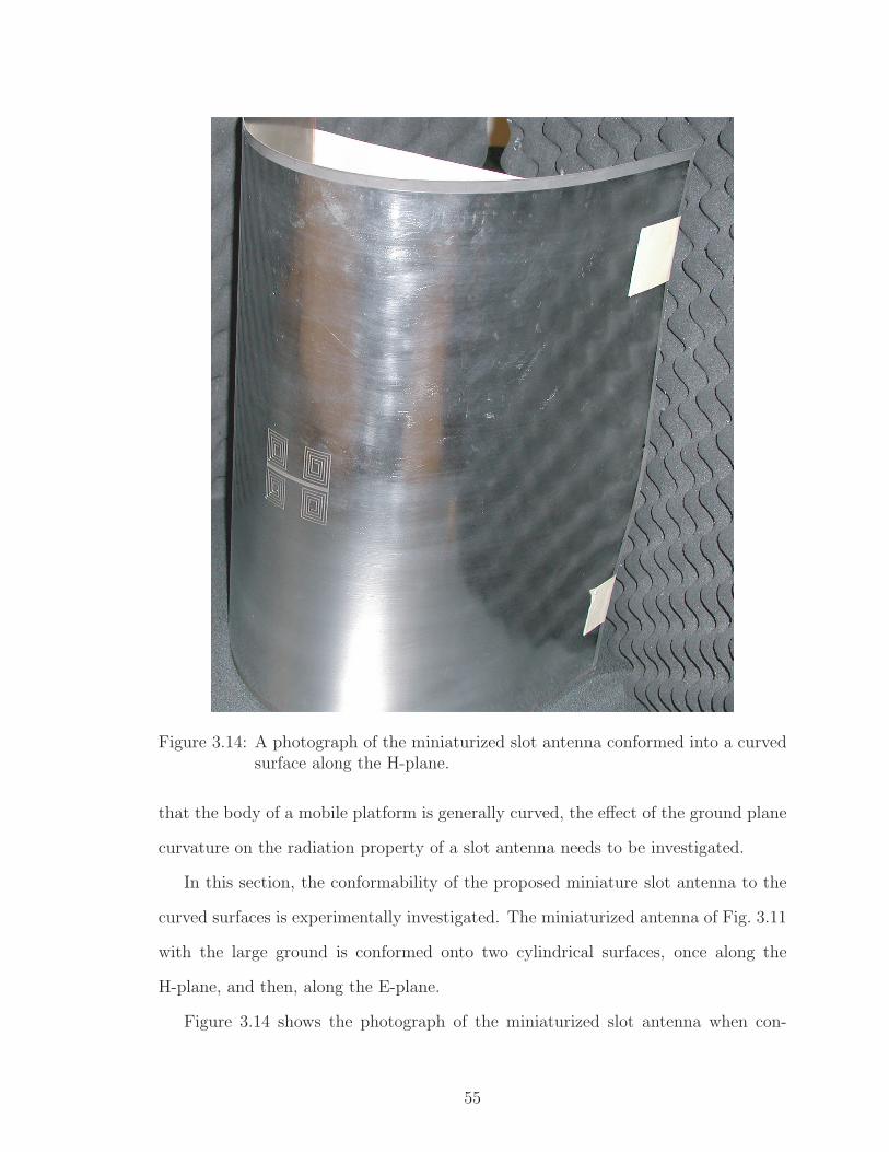
Figure 3.14: A photograph of the miniaturized slot antenna conformed into a curvedsurface along the H-plane.
that the body of a mobile platform is generally curved, the effect of the ground plane
curvature on the radiation property of a slot antenna needs to be investigated.
In this section, the conformability of the proposed miniature slot antenna to the
curved surfaces is experimentally investigated. The miniaturized antenna of Fig. 3.11
with the large ground is conformed onto two cylindrical surfaces, once along the
H-plane, and then, along the E-plane.
Figure 3.14 shows the photograph of the miniaturized slot antenna when con-
55
formed to a cylindrical surface along its H-plane. The variation of the input return
loss of the conformed antenna is negligible as compared to the planar ground. The ra-
diation pattern of the curved antenna of Fig. 3.14 is measured and plotted in Fig. 3.15.
Figure 3.15 also includes the measured radiation pattern of the original miniature an-
tenna without the curvature for comparison. As seen in this figure, the H-plane
radiation pattern slightly changes, and it exhibits some asymmetry. Changes in the
E-plane pattern are minimal since the curvature does not incur any asymmetry on
this plane.
The miniaturized slot antenna is then conformed to a cylindrical surface along the
E-plane as depicted in Fig. 3.16. The return loss of the antenna in this configuration
does not change either. The radiation pattern of the E-plane conformed antenna was
measured for both principle planes of E and H and shown in Figs 3.17(a) and (b),
respectively. These patterns are again compared with the radiation pattern on the
same antenna without the curvature. As seen in Fig. 3.17, the H-plane pattern of
the curved antenna is changed slightly, whereas the E-plane pattern experiences a
noteworthy change. As Fig. 3.17(b) shows, the E-plane nulls of the original pattern
are filled considerably. As alluded to in earlier discussions and will be elaborated
in Appendix A, a simulation with finite ground plane predicts a constant E-plane
pattern for the slot antenna. But due to the finite size ground plane, the equivalent
magnetic currents flowing in opposite directions, slightly above and below the ground
plane, tend to cancel each other’s radiated fields and create two nulls. Obviously,
the curvature in the E-plane partially blocks the radiation by one of these opposing
magnetic currents at θ = ±90. That is why the null in the E-plane pattern is filled
considerably.
The above study shows that conforming the miniaturized slot antenna to a curved
plane does not deteriorate the pattern of the antenna so far as the radius of the cur-
vature is much larger than the dimensions of the antenna. Based on this preliminary
56
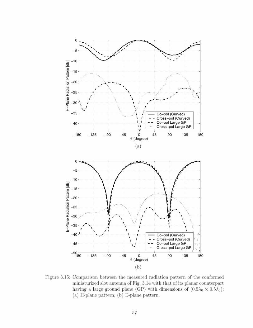
−180 −135 −90 −45 0 45 90 135 180
−40
−35
−30
−25
−20
−15
−10
−5
0
θ (degree)
H−P
lane
Rad
iatio
n P
atte
rn [d
B]
Co−pol (Curved)Cross−pol (Curved)Co−pol Large GPCross−pol Large GP
(a)
−180 −135 −90 −45 0 45 90 135 180−50
−45
−40
−35
−30
−25
−20
−15
−10
−5
0
θ (degree)
E−P
lane
Rad
iatio
n P
atte
rn [d
B]
Co−pol (Curved)Cross−pol (Curved)Co−pol Large GPCross−pol Large GP
(b)
Figure 3.15: Comparison between the measured radiation pattern of the conformedminiaturized slot antenna of Fig. 3.14 with that of its planar counterparthaving a large ground plane (GP) with dimensions of (0.5λ0 × 0.5λ0):(a) H-plane pattern, (b) E-plane pattern.
57
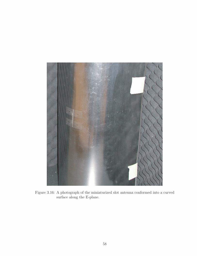
Figure 3.16: A photograph of the miniaturized slot antenna conformed into a curvedsurface along the E-plane.
58
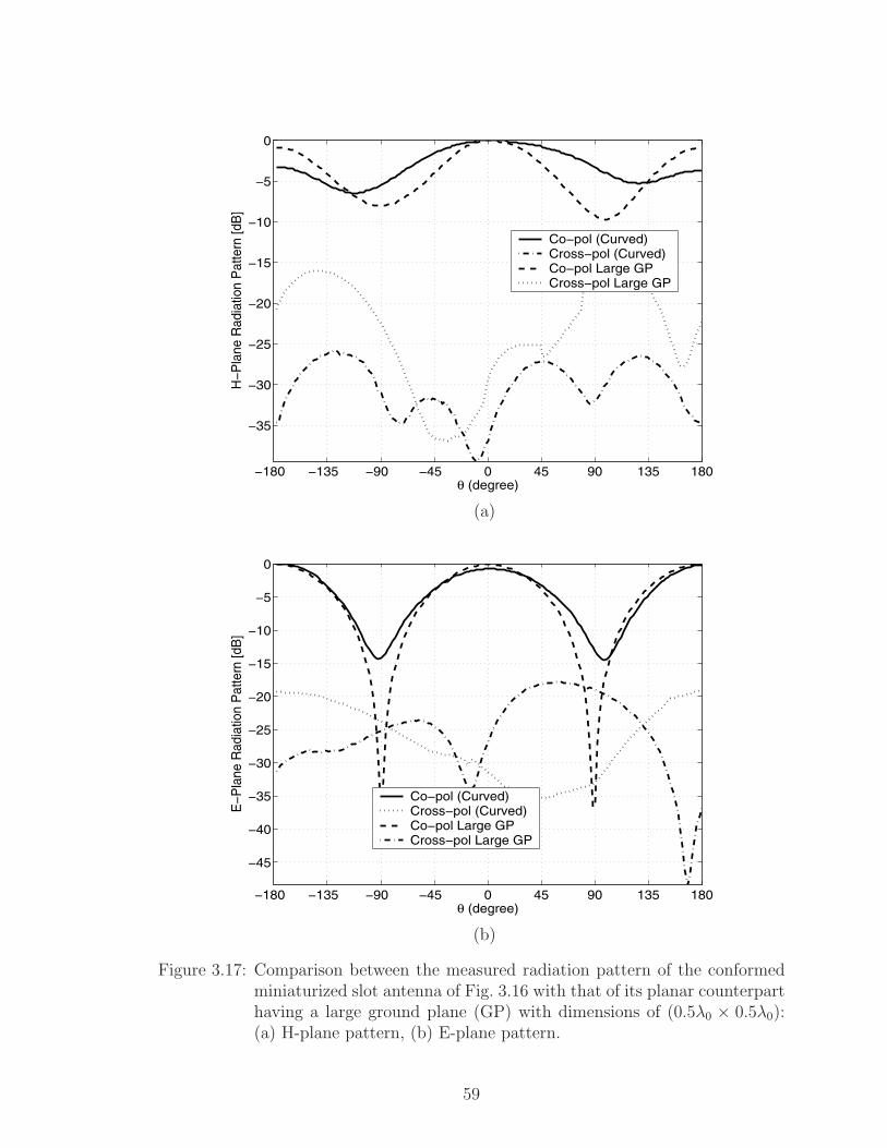
−180 −135 −90 −45 0 45 90 135 180
−35
−30
−25
−20
−15
−10
−5
0
θ (degree)
H−P
lane
Rad
iatio
n P
atte
rn [d
B]
Co−pol (Curved)Cross−pol (Curved)Co−pol Large GPCross−pol Large GP
(a)
−180 −135 −90 −45 0 45 90 135 180
−45
−40
−35
−30
−25
−20
−15
−10
−5
0
θ (degree)
E−P
lane
Rad
iatio
n P
atte
rn [d
B]
Co−pol (Curved)Cross−pol (Curved)Co−pol Large GPCross−pol Large GP
(b)
Figure 3.17: Comparison between the measured radiation pattern of the conformedminiaturized slot antenna of Fig. 3.16 with that of its planar counterparthaving a large ground plane (GP) with dimensions of (0.5λ0 × 0.5λ0):(a) H-plane pattern, (b) E-plane pattern.
59

study, we expect that the effect of the curvature on the cavity backed miniaturized
slot antenna to be tolerable.
3.7 Conclusion
In this chapter, a procedure for designing a new class of miniaturized slot antennas
was proposed. In this design the area occupied by the antenna can be chosen to be
arbitrarily small, depending on the applications at hand and the trade-off between
the antenna size and the required bandwidth. As an example, an antenna with the
dimensions 0.05λ0 × 0.05λ0 was designed at 300 MHz and perfectly matched to a
50 Ω transmission line. In this prototype, a substrate with a low dielectric constant
of εr = 2.2 was used to ensure that the dielectric material would not contribute to
the antenna miniaturization. An equivalent circuit for the antenna was developed,
which provided the guidelines necessary for designing a compact loss-less matching
network for the antenna. To validate the design procedure, a prototype antenna was
fabricated and measured at 300 MHz. A perfect match for this very small antenna
was demonstrated with a moderate gain of −3.0 dBi when the antenna is fabricated
on a very small ground plane with the approximate dimensions of 0.2λ0 × 0.2λ0. The
gain of this antenna can increase to that of a half-wave dipole when a slightly larger
ground plane of about 0.5λ0×0.5λ0 is used. The fractional bandwidth for this antenna
was measured to be 0.34%.
60

CHAPTER 4
Bandwidth Enhancement of Miniaturized Slot
Antennas Using Folded, Complementary and
Self-Complementary Realizations
4.1 Introduction
The notion of antenna miniaturization coincides with the narrow bandwidth and
low efficiency. These two adverse impacts of miniaturization make miniaturized an-
tennas very difficult to match. Among the above ramifications, narrow bandwidth
has particularly been the subject of additional interests, and been referred to as one
of the fundamental limitation of small antennas [1, 2, 3, 8, 9, 10]. Given that a small
antenna can be enclosed within a sphere with a certain radius, the above literature
introduces a limit on the bandwidth of these antennas. The limit can be approached
only if the antenna is occupying the whole spherical volume. If not, which is the case
for planar antennas, the fundamental limit gives a very loose upper bound for the
bandwidth. Thus, one may attempt to enhance the bandwidth of a planar miniature
antenna and still not to exceed the fundamental limit.
Nevertheless, practical aspects of antenna miniaturization have received significant
attention in recent years. In Chapter 3, we have proposed a new class of efficient
61
miniaturized slot antennas which can be easily matched without the need for external
matching networks. The topology of a typical miniaturized slot antenna of this class
is shown in Fig. 4.1. The miniature design is achieved by introducing symmetric
inductive loadings at both ends of a short radiating slot section to create a voltage
discontinuity along a resonant slot-line. An important advantage of this topology is
that the antenna size, depending on the application at hand, can be chosen almost
arbitrarily small at the cost of reduction in bandwidth and efficiency. As an example,
the design of a miniaturized antenna with dimensions as small as 0.05λ0 × 0.05λ0
showing a fairly high gain of −3 dBi was demonstrated in Chapter 3.
Resonant antennas in general, and resonant slot antennas in particular, are inher-
ently narrow band. Obviously, further bandwidth reduction is expected for miniature
slotted structures. In addition to a narrow bandwidth, another important issue re-
garding slot antennas is the ground plane size and its impact on antenna gain and
efficiency. The effects of a finite size ground plane on the radiation characteristics
of the miniaturized slot antennas have been experimentally studied in Chapter 2
and Chapter 3. Additional investigation of the effects of finite size ground plane is
presented in Appendix A.
This chapter focuses on two main objectives. First is to introduce methodologies
to enhance the bandwidth of the miniaturized slot antenna presented in Chapter 3,
and second is to mitigate the drawbacks related to the small size ground plane. The
finite size ground becomes a critical issue in cases where a large metallic body is not
available to be used for the slot ground plane.
In order to fulfill the first objective of this chapter, namely, the bandwidth en-
hancement of the miniature antenna, folded and self-complementary configurations
are examined. Folded and self-complementary structures are considered as two ef-
fective approaches to increase the bandwidth of miniaturized antennas. A folded
structure may be introduced to significantly increase the bandwidth of a miniatur-
62
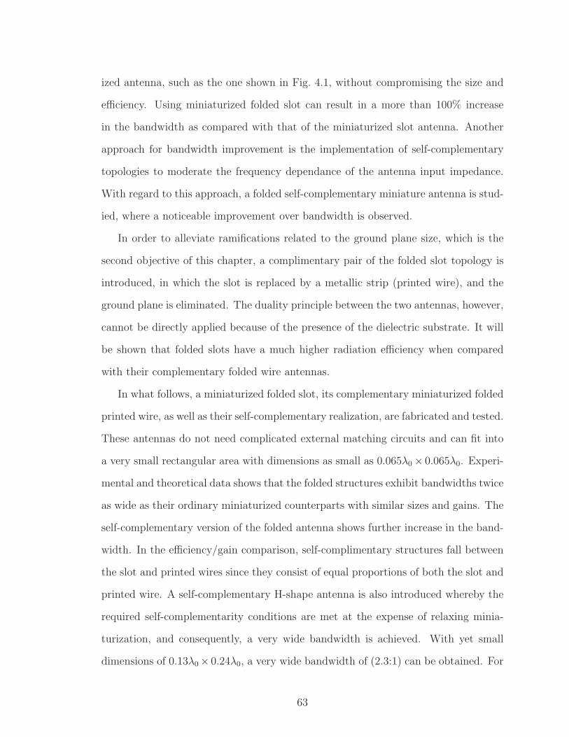
ized antenna, such as the one shown in Fig. 4.1, without compromising the size and
efficiency. Using miniaturized folded slot can result in a more than 100% increase
in the bandwidth as compared with that of the miniaturized slot antenna. Another
approach for bandwidth improvement is the implementation of self-complementary
topologies to moderate the frequency dependance of the antenna input impedance.
With regard to this approach, a folded self-complementary miniature antenna is stud-
ied, where a noticeable improvement over bandwidth is observed.
In order to alleviate ramifications related to the ground plane size, which is the
second objective of this chapter, a complimentary pair of the folded slot topology is
introduced, in which the slot is replaced by a metallic strip (printed wire), and the
ground plane is eliminated. The duality principle between the two antennas, however,
cannot be directly applied because of the presence of the dielectric substrate. It will
be shown that folded slots have a much higher radiation efficiency when compared
with their complementary folded wire antennas.
In what follows, a miniaturized folded slot, its complementary miniaturized folded
printed wire, as well as their self-complementary realization, are fabricated and tested.
These antennas do not need complicated external matching circuits and can fit into
a very small rectangular area with dimensions as small as 0.065λ0 × 0.065λ0. Experi-
mental and theoretical data shows that the folded structures exhibit bandwidths twice
as wide as their ordinary miniaturized counterparts with similar sizes and gains. The
self-complementary version of the folded antenna shows further increase in the band-
width. In the efficiency/gain comparison, self-complimentary structures fall between
the slot and printed wires since they consist of equal proportions of both the slot and
printed wire. A self-complementary H-shape antenna is also introduced whereby the
required self-complementarity conditions are met at the expense of relaxing minia-
turization, and consequently, a very wide bandwidth is achieved. With yet small
dimensions of 0.13λ0 × 0.24λ0, a very wide bandwidth of (2.3:1) can be obtained. For
63
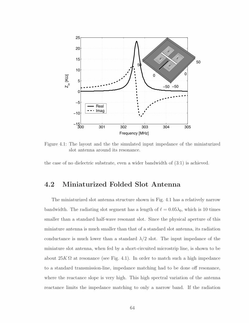
300 301 302 303 304 305−15
−10
−5
0
5
10
15
20
25
Frequency [MHz]
Zin
[KΩ
]
RealImag
−50
0
50
−50
0
50
Figure 4.1: The layout and the the simulated input impedance of the miniaturizedslot antenna around its resonance.
the case of no dielectric substrate, even a wider bandwidth of (3:1) is achieved.
4.2 Miniaturized Folded Slot Antenna
The miniaturized slot antenna structure shown in Fig. 4.1 has a relatively narrow
bandwidth. The radiating slot segment has a length of = 0.05λ0, which is 10 times
smaller than a standard half-wave resonant slot. Since the physical aperture of this
miniature antenna is much smaller than that of a standard slot antenna, its radiation
conductance is much lower than a standard λ/2 slot. The input impedance of the
miniature slot antenna, when fed by a short-circuited microstrip line, is shown to be
about 25K Ω at resonance (see Fig. 4.1). In order to match such a high impedance
to a standard transmission-line, impedance matching had to be done off resonance,
where the reactance slope is very high. This high spectral variation of the antenna
reactance limits the impedance matching to only a narrow band. If the radiation
64
conductance of the miniaturized slot antenna can be increased without significantly
increasing the antenna size, impedance matching over a wider bandwidth can be
achieved. Increasing the physical aperture by means of introducing a suitable folded
structure seems to be an appropriate approach since the antenna aperture readily
increases, while the antenna size can be kept almost the same.
The impedance of a resonant folded dipole antenna is related to that of a dipole
antenna by [34, 21]
Zfolded−dipolein = 4 Zdipole
in (4.1)
Using Bookers’ relation [35], the input impedance of a resonant slot (magnetic) dipole
can be obtained from its complementary pair and vice versa as
Zfolded−slotin =
η2
4
1
Zfolded−dipolein
=Zslot
in
4(4.2)
Equation (4.2) shows that the input impedance of a folded slot is four times smaller
than that of the standard slot dipole. Thus, the impedance of a miniaturized folded
slot is expected to be much closer to the impedance of standard transmission-lines,
and thus easier to match.
Figure 4.2 shows the proposed miniaturized folded slot topology fed by a CPW
line. The same figure shows the simulated input impedance as a function of frequency.
Dimensions of the folded prototype are chosen to be the same as those of the miniatur-
ized antenna in Fig. 4.1. This antenna occupies an area of 6cm× 6cm. The resonant
frequency of this folded antenna, however, is slightly higher than that of the origi-
nal miniaturized slot. As illustrated, the miniature folded-slot impedance is reduced
from about 25 KΩ for the original design to 6 KΩ, which is easier to match to a 50 Ω
line. Moreover, for the folded antenna, the reactance slope of the input impedance is
much lower at the frequency where the real part of the antenna impedance is 50 Ω,
indicating the possibility of impedance matching over a wider frequency band.
65
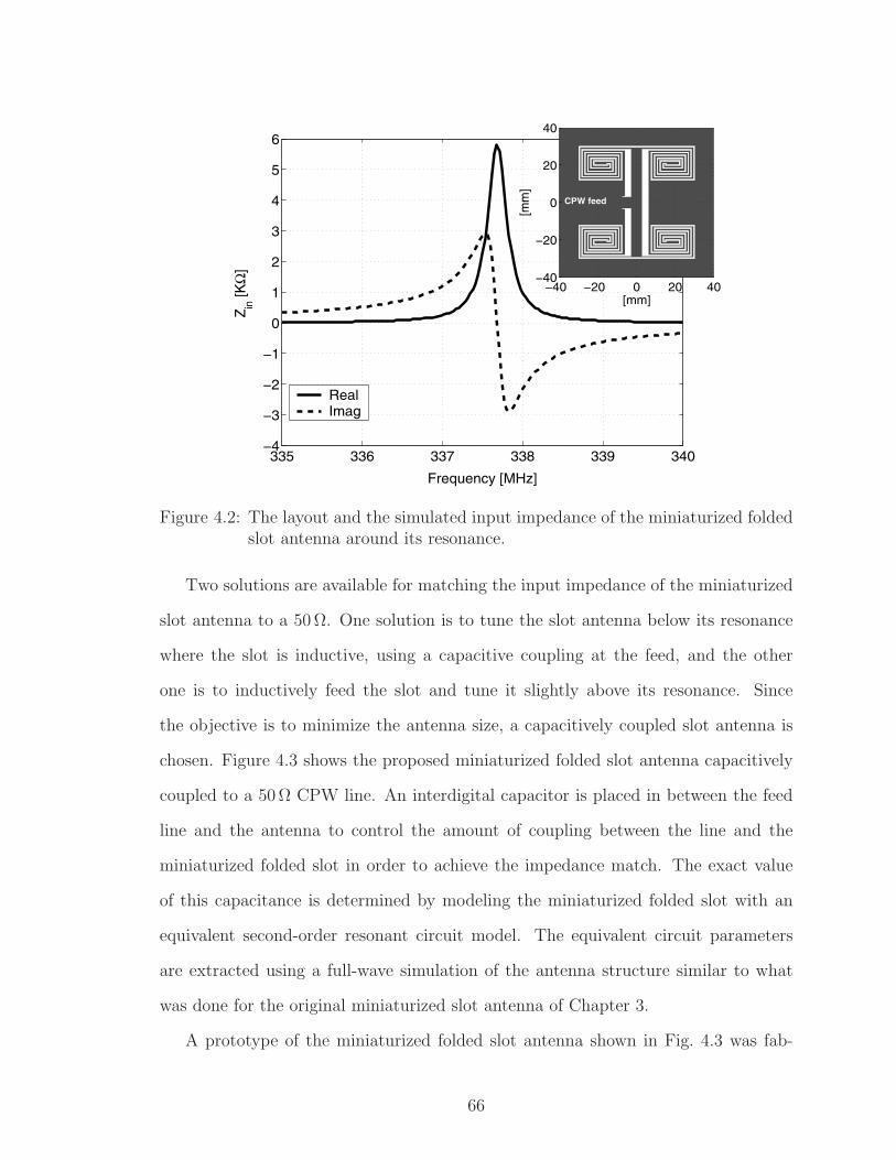
335 336 337 338 339 340−4
−3
−2
−1
0
1
2
3
4
5
6
Frequency [MHz]
Zin
[KΩ
]
RealImag
−40 −20 0 20 40−40
−20
0
20
40
[mm]
[mm
]CPW Feed CPW feed
Figure 4.2: The layout and the simulated input impedance of the miniaturized foldedslot antenna around its resonance.
Two solutions are available for matching the input impedance of the miniaturized
slot antenna to a 50 Ω. One solution is to tune the slot antenna below its resonance
where the slot is inductive, using a capacitive coupling at the feed, and the other
one is to inductively feed the slot and tune it slightly above its resonance. Since
the objective is to minimize the antenna size, a capacitively coupled slot antenna is
chosen. Figure 4.3 shows the proposed miniaturized folded slot antenna capacitively
coupled to a 50 Ω CPW line. An interdigital capacitor is placed in between the feed
line and the antenna to control the amount of coupling between the line and the
miniaturized folded slot in order to achieve the impedance match. The exact value
of this capacitance is determined by modeling the miniaturized folded slot with an
equivalent second-order resonant circuit model. The equivalent circuit parameters
are extracted using a full-wave simulation of the antenna structure similar to what
was done for the original miniaturized slot antenna of Chapter 3.
A prototype of the miniaturized folded slot antenna shown in Fig. 4.3 was fab-
66
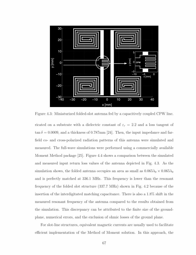
−40 −30 −20 −10 0 10 20 30 40−30
−20
−10
0
10
20
30
y [m
m]
x [mm]
−10 −5 0−5
0
5
x [mm]
y [m
m]
CPW
Figure 4.3: Miniaturized folded-slot antenna fed by a capacitively coupled CPW line.
ricated on a substrate with a dielectric constant of εr = 2.2 and a loss tangent of
tan δ = 0.0009, and a thickness of 0.787mm [24]. Then, the input impedance and far-
field co- and cross-polarized radiation patterns of this antenna were simulated and
measured. The full-wave simulations were performed using a commercially available
Moment Method package [25]. Figure 4.4 shows a comparison between the simulated
and measured input return loss values of the antenna depicted in Fig. 4.3. As the
simulation shows, the folded antenna occupies an area as small as 0.065λ0 × 0.065λ0
and is perfectly matched at 336.1 MHz. This frequency is lower than the resonant
frequency of the folded slot structure (337.7 MHz) shown in Fig. 4.2 because of the
insertion of the interdigitated matching capacitance. There is also a 1.8% shift in the
measured resonant frequency of the antenna compared to the results obtained from
the simulation. This discrepancy can be attributed to the finite size of the ground-
plane, numerical errors, and the exclusion of ohmic losses of the ground plane.
For slot-line structures, equivalent magnetic currents are usually used to facilitate
efficient implementation of the Method of Moment solution. In this approach, the
67
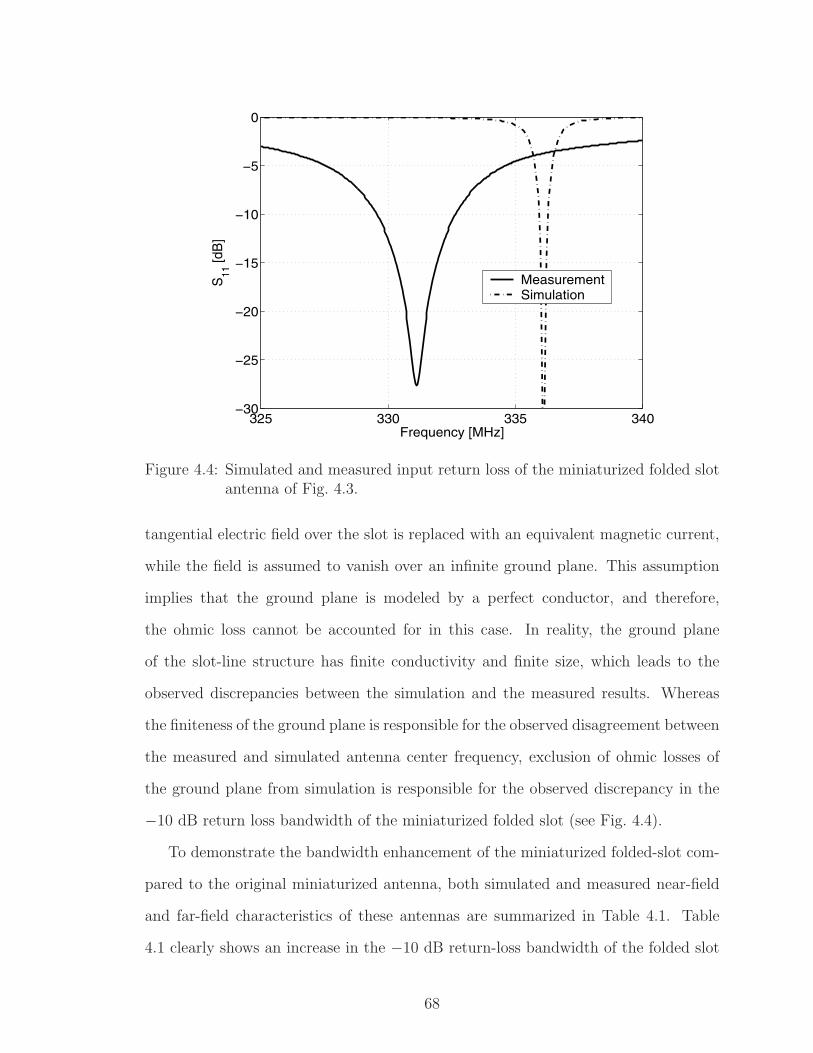
325 330 335 340−30
−25
−20
−15
−10
−5
0
Frequency [MHz]
S11
[dB
]
MeasurementSimulation
Figure 4.4: Simulated and measured input return loss of the miniaturized folded slotantenna of Fig. 4.3.
tangential electric field over the slot is replaced with an equivalent magnetic current,
while the field is assumed to vanish over an infinite ground plane. This assumption
implies that the ground plane is modeled by a perfect conductor, and therefore,
the ohmic loss cannot be accounted for in this case. In reality, the ground plane
of the slot-line structure has finite conductivity and finite size, which leads to the
observed discrepancies between the simulation and the measured results. Whereas
the finiteness of the ground plane is responsible for the observed disagreement between
the measured and simulated antenna center frequency, exclusion of ohmic losses of
the ground plane from simulation is responsible for the observed discrepancy in the
−10 dB return loss bandwidth of the miniaturized folded slot (see Fig. 4.4).
To demonstrate the bandwidth enhancement of the miniaturized folded-slot com-
pared to the original miniaturized antenna, both simulated and measured near-field
and far-field characteristics of these antennas are summarized in Table 4.1. Table
4.1 clearly shows an increase in the −10 dB return-loss bandwidth of the folded slot
68
antenna over the original antenna from 0.34% to 0.93%. The gains of these anten-
nas were measured against a standard half wavelength dipole antenna. The gain of
the folded and original miniaturized slot antennas were, respectively, measured to
be −2.7 dBi and −3.0 dBi. The measured values of the gains are lower than the
simulated results. This again difference can be attributed to the the ohmic loss and
finite size of the ground plane which have not been accounted for in the simulation.
Finally, the H-plane and E-plane radiation patterns of the miniaturized folded-
slot antenna were measured in the anechoic chamber of the University of Michigan
and are shown in Fig. 4.5. For the E-plane pattern, Eθ(θ) was measured in the
φ = 0 plane. The measurement of Eφ(θ) in the φ = 90 plane provides the H-plane
pattern of the antenna. In theory, a null should exist in the H-plane pattern of an
infinitesimal folded-slot, since the ground plane forces the tangential electric field
of Eφ(θ = 90) = 0 at φ = 90 to vanish. This deep null, however, is not observed
because of the finite dimensions of the ground plane. When the ground is not extended
to infinity, the radiation by edges would fill the null. On the other hand, a null is
created in the E-plane pattern, whereas the theory predicts a uniform pattern. This
phenomenon is also caused by the finite dimensions of the ground plane. Based on
the equivalence principle, the magnetic currents on the upper and lower half space
flow in two opposite directions and create out of phase normal electric fields on the
antenna plane (θ = 0). When the ground plane is infinite, the lower and upper half
spaces are decoupled, and no cancellation occurs. The cross-polarization component
of the radiation pattern is small because of the symmetry of the structure in the
principal E- and H-planes. The observed minor cross-polarized radiation is caused by
the edges of the finite size ground plane and the re-radiation of the near-field of the
antenna by the feeding cable.
69
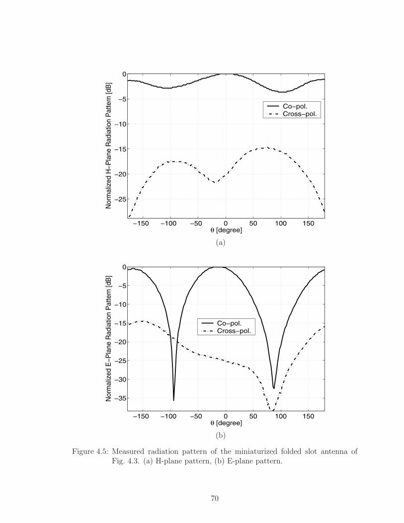
−150 −100 −50 0 50 100 150
−25
−20
−15
−10
−5
0
θ [degree]
Nor
mal
ized
H−P
lane
Rad
iatio
n P
atte
rn [d
B]
Co−pol.Cross−pol.
(a)
−150 −100 −50 0 50 100 150
−35
−30
−25
−20
−15
−10
−5
0
θ [degree]
Nor
mal
ized
E−P
lane
Rad
iatio
n P
atte
rn [d
B]
Co−pol.Cross−pol.
(b)
Figure 4.5: Measured radiation pattern of the miniaturized folded slot antenna ofFig. 4.3. (a) H-plane pattern, (b) E-plane pattern.
70
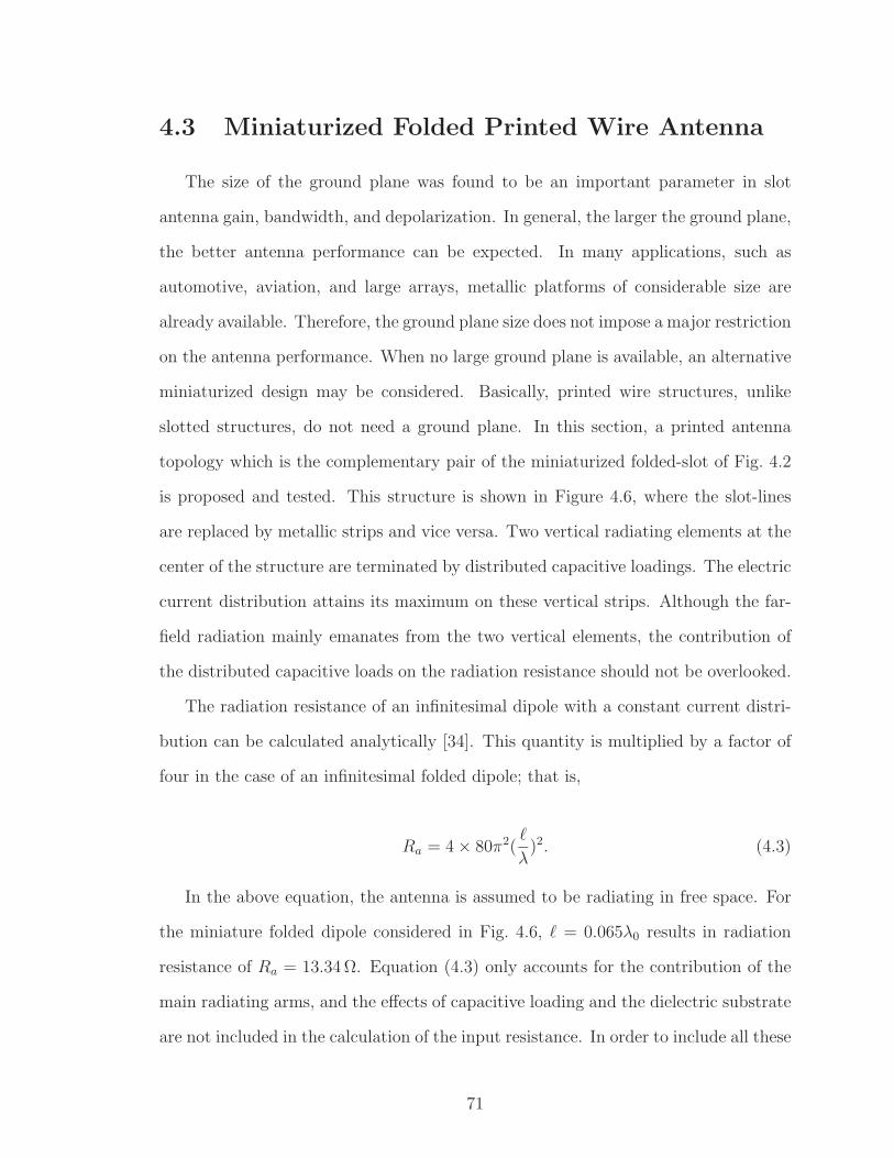
4.3 Miniaturized Folded Printed Wire Antenna
The size of the ground plane was found to be an important parameter in slot
antenna gain, bandwidth, and depolarization. In general, the larger the ground plane,
the better antenna performance can be expected. In many applications, such as
automotive, aviation, and large arrays, metallic platforms of considerable size are
already available. Therefore, the ground plane size does not impose a major restriction
on the antenna performance. When no large ground plane is available, an alternative
miniaturized design may be considered. Basically, printed wire structures, unlike
slotted structures, do not need a ground plane. In this section, a printed antenna
topology which is the complementary pair of the miniaturized folded-slot of Fig. 4.2
is proposed and tested. This structure is shown in Figure 4.6, where the slot-lines
are replaced by metallic strips and vice versa. Two vertical radiating elements at the
center of the structure are terminated by distributed capacitive loadings. The electric
current distribution attains its maximum on these vertical strips. Although the far-
field radiation mainly emanates from the two vertical elements, the contribution of
the distributed capacitive loads on the radiation resistance should not be overlooked.
The radiation resistance of an infinitesimal dipole with a constant current distri-
bution can be calculated analytically [34]. This quantity is multiplied by a factor of
four in the case of an infinitesimal folded dipole; that is,
Ra = 4 × 80π2(
λ)2. (4.3)
In the above equation, the antenna is assumed to be radiating in free space. For
the miniature folded dipole considered in Fig. 4.6, = 0.065λ0 results in radiation
resistance of Ra = 13.34 Ω. Equation (4.3) only accounts for the contribution of the
main radiating arms, and the effects of capacitive loading and the dielectric substrate
are not included in the calculation of the input resistance. In order to include all these
71
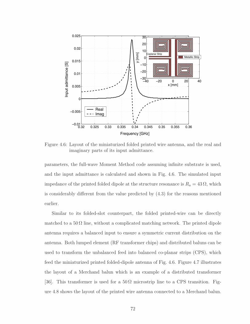
0.32 0.325 0.33 0.335 0.34 0.345 0.35 0.355 0.36−0.01
−0.005
0
0.005
0.01
0.015
0.02
0.025
Frequency [GHz]
Inp
ut
ad
mitt
an
ce [
S]
−40 −20 0 20 40−30
−20
−10
0
10
20
30
x [mm]
y [m
m]
RealImag
Metallic StripCoplanar Strip
Figure 4.6: Layout of the miniaturized folded printed wire antenna, and the real andimaginary parts of its input admittance.
parameters, the full-wave Moment Method code assuming infinite substrate is used,
and the input admittance is calculated and shown in Fig. 4.6. The simulated input
impedance of the printed folded dipole at the structure resonance is Ra = 43 Ω, which
is considerably different from the value predicted by (4.3) for the reasons mentioned
earlier.
Similar to its folded-slot counterpart, the folded printed-wire can be directly
matched to a 50 Ω line, without a complicated matching network. The printed dipole
antenna requires a balanced input to ensure a symmetric current distribution on the
antenna. Both lumped element (RF transformer chips) and distributed baluns can be
used to transform the unbalanced feed into balanced co-planar strips (CPS), which
feed the miniaturized printed folded-dipole antenna of Fig. 4.6. Figure 4.7 illustrates
the layout of a Merchand balun which is an example of a distributed transformer
[36]. This transformer is used for a 50 Ω microstrip line to a CPS transition. Fig-
ure 4.8 shows the layout of the printed wire antenna connected to a Merchand balun.
72
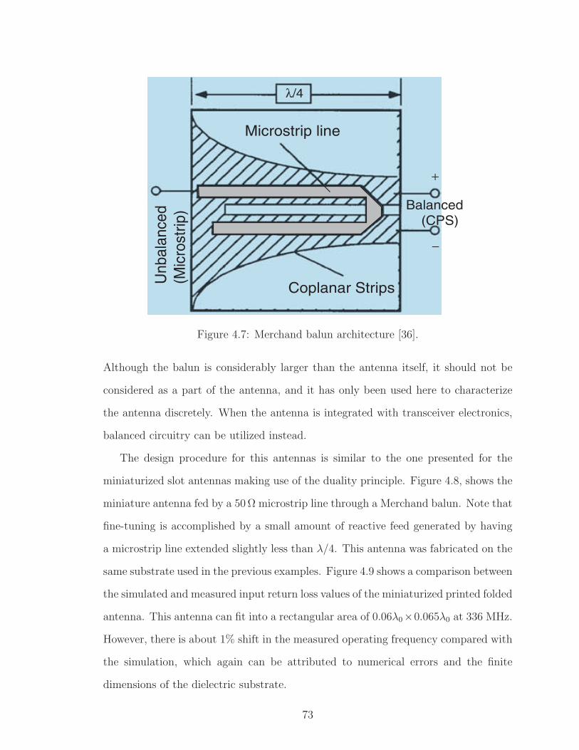
Microstrip line
Coplanar Strips
Balanced (CPS)
Unb
alan
ced
(Mic
rost
rip)
Figure 4.7: Merchand balun architecture [36].
Although the balun is considerably larger than the antenna itself, it should not be
considered as a part of the antenna, and it has only been used here to characterize
the antenna discretely. When the antenna is integrated with transceiver electronics,
balanced circuitry can be utilized instead.
The design procedure for this antennas is similar to the one presented for the
miniaturized slot antennas making use of the duality principle. Figure 4.8, shows the
miniature antenna fed by a 50 Ω microstrip line through a Merchand balun. Note that
fine-tuning is accomplished by a small amount of reactive feed generated by having
a microstrip line extended slightly less than λ/4. This antenna was fabricated on the
same substrate used in the previous examples. Figure 4.9 shows a comparison between
the simulated and measured input return loss values of the miniaturized printed folded
antenna. This antenna can fit into a rectangular area of 0.06λ0×0.065λ0 at 336 MHz.
However, there is about 1% shift in the measured operating frequency compared with
the simulation, which again can be attributed to numerical errors and the finite
dimensions of the dielectric substrate.
73
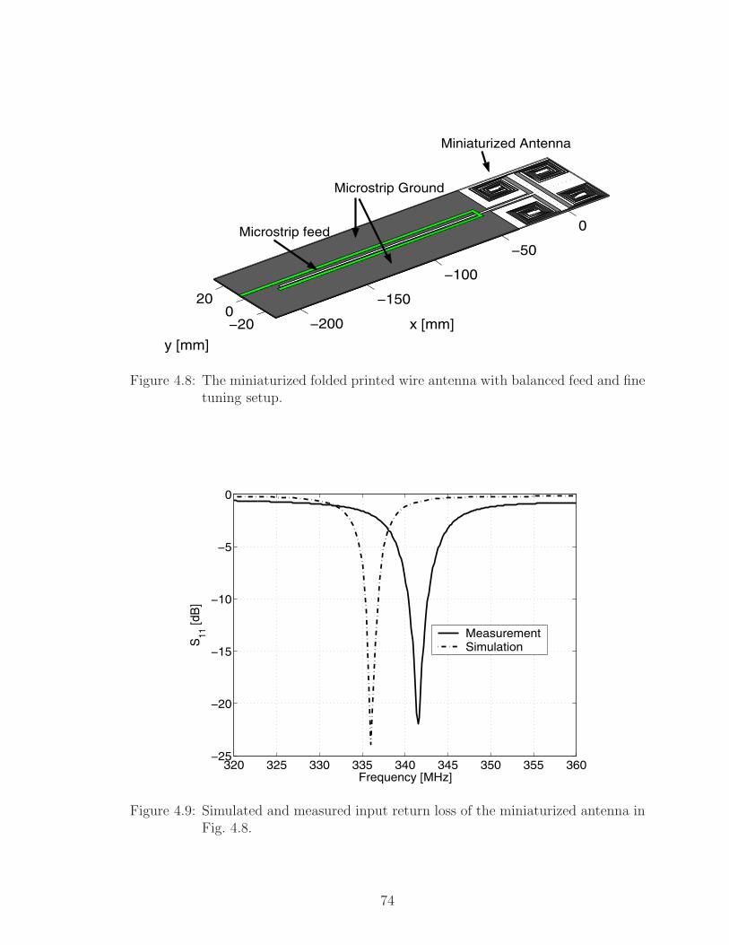
−200
−150
−100
−50
0
−200
20
x [mm]
y [mm]
Microstrip feed
Microstrip Ground
Miniaturized Antenna
Figure 4.8: The miniaturized folded printed wire antenna with balanced feed and finetuning setup.
320 325 330 335 340 345 350 355 360−25
−20
−15
−10
−5
0
Frequency [MHz]
S11
[dB
]
MeasurementSimulation
Figure 4.9: Simulated and measured input return loss of the miniaturized antenna inFig. 4.8.
74
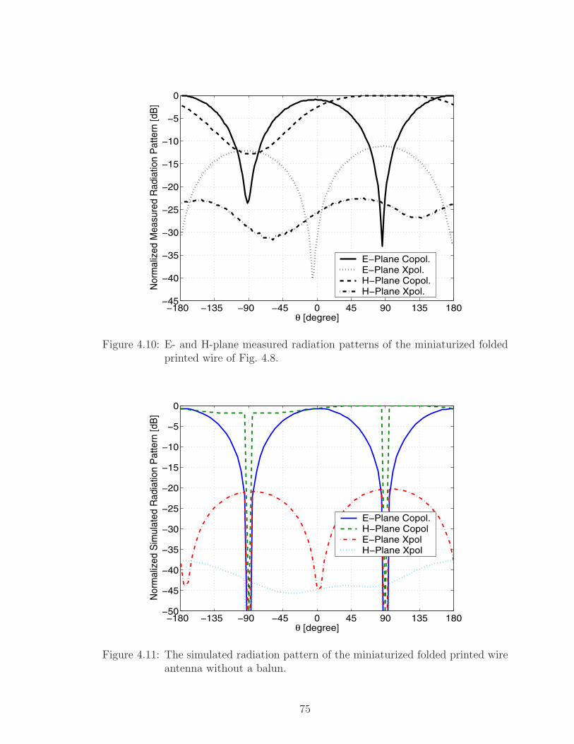
−180 −135 −90 −45 0 45 90 135 180−45
−40
−35
−30
−25
−20
−15
−10
−5
0
θ [degree]
Nor
mal
ized
Mea
sure
d R
adia
tion
Pat
tern
[dB
]
E−Plane Copol.E−Plane Xpol.H−Plane Copol.H−Plane Xpol.
Figure 4.10: E- and H-plane measured radiation patterns of the miniaturized foldedprinted wire of Fig. 4.8.
−180 −135 −90 −45 0 45 90 135 180−50
−45
−40
−35
−30
−25
−20
−15
−10
−5
0
θ [degree]
Nor
mal
ized
Sim
ulat
ed R
adia
tion
Pat
tern
[dB
]
E−Plane Copol.H−Plane CopolE−Plane XpolH−Plane Xpol
Figure 4.11: The simulated radiation pattern of the miniaturized folded printed wireantenna without a balun.
75
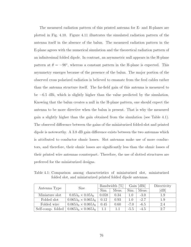
The measured radiation pattern of this printed antenna for E- and H-planes are
plotted in Fig. 4.10. Figure 4.11 illustrates the simulated radiation pattern of the
antenna itself in the absence of the balun. The measured radiation pattern in the
E-plane agrees with the numerical simulation and the theoretical radiation pattern of
an infinitesimal folded dipole. In contrast, an asymmetric null appears in the H-plane
pattern at θ = −90, whereas a constant pattern in the H-plane is expected. This
asymmetry emerges because of the presence of the balun. The major portion of the
observed cross polarized radiation is believed to emanate from the feed cables rather
than the antenna structure itself. The far-field gain of this antenna is measured to
be −6.5 dBi, which is slightly higher than the value predicted by the simulation.
Knowing that the balun creates a null in the H-plane pattern, one should expect the
antenna to be more directive when the balun is present. That is why the measured
gain a slightly higher than the gain obtained from the simulation (see Table 4.1).
The observed difference between the gains of the miniaturized folded-slot and printed
dipole is noteworthy. A 3.8 dB gain difference exists between the two antennas which
is attributed to conductor ohmic losses. Slot antennas make use of more conduc-
tors, and therefore, their ohmic losses are significantly less than the ohmic losses of
their printed wire antennas counterpart. Therefore, the use of slotted structures are
preferred for the miniaturized designs.
Table 4.1: Comparison among characteristics of miniaturized slot, miniaturizedfolded slot, and miniaturized printed folded dipole antennas.
Antenna Type SizeBandwidth [%] Gain [dBi] Directivity
[dB]Sim. Meas. Sim. Meas.Miniature slot 0.05λ0 × 0.05λ0 0.058 0.34 1.0 -3.0 1.9
Folded slot 0.065λ0 × 0.065λ0 0.12 0.93 1.0 -2.7 1.9Folded wire 0.065λ0 × 0.065λ0 0.45 0.60 -7.0 -6.5 2.4
Self-comp. folded 0.065λ0 × 0.065λ0 1.1 1.1 -5.5 -4.5 2.7
76

4.4 Miniaturized Self-Complementary Folded An-
tenna
The use of self-complimentary antennas has been suggested to obtain antennas
with frequency-independent input impedances [37]. The basic idea stems from the
fact that these structures consist of two sections that are dual of each other. There-
fore, the reactive parts of these two subsections tend to cancel each other, which
leads to a purely real input impedance over the frequency band. In reality, however,
a self-complementary radiating structure needs to be truncated, and this truncation
by itself deteriorates the performance of a self-complementary design. The extent of
this deterioration depends on the geometry as well as the truncation extent. Trun-
cation becomes even more important when miniaturized antennas are considered.
Apparently, miniaturized self-complementary antennas are subject to a very tight
truncation whose effect should be closely examined.
Another important assumption in self-complimentary structures is that the an-
tenna should radiate in the free space or homogeneous media. Consequently, the
introduction of a dielectric medium would violate the required condition for self-
complementarity, and thus, the prescribed theoretical results may not be achieved.
Figure 4.12 shows a self-complementary pair of the two previously introduced
folded antennas where the top half of the structure is similar to that of the folded
printed wire in Fig. 4.6, and the lower half resembles the folded slot of Fig. 4.2. This
structure is excited through self-complementary transmission-line which resembles an
asymmetric CPW waveguide. The characteristic impedance of this transmission-line
is Zc ≈ 60π/√
εr, given that a dielectric substrate is present. This antenna has the
same dimensions as the two previously introduced structures and is fabricated on
the same Duroid dielectric substrate. In order to analyze the structure, the two-
port antenna structure shown in Fig. 4.12 is simulated using the Method of Moment
77
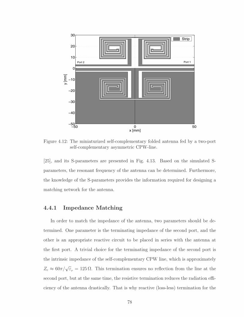
−50 0 50−50
−40
−30
−20
−10
0
10
20
30
x [mm]
y [m
m]
Strip
Port 1 Port 2
Figure 4.12: The miniaturized self-complementary folded antenna fed by a two-portself-complementary asymmetric CPW-line.
[25], and its S-parameters are presented in Fig. 4.13. Based on the simulated S-
parameters, the resonant frequency of the antenna can be determined. Furthermore,
the knowledge of the S-parameters provides the information required for designing a
matching network for the antenna.
4.4.1 Impedance Matching
In order to match the impedance of the antenna, two parameters should be de-
termined. One parameter is the terminating impedance of the second port, and the
other is an appropriate reactive circuit to be placed in series with the antenna at
the first port. A trivial choice for the terminating impedance of the second port is
the intrinsic impedance of the self-complementary CPW line, which is approximately
Zc ≈ 60π/√
εr = 125 Ω. This termination ensures no reflection from the line at the
second port, but at the same time, the resistive termination reduces the radiation effi-
ciency of the antenna drastically. That is why reactive (loss-less) termination for the
78
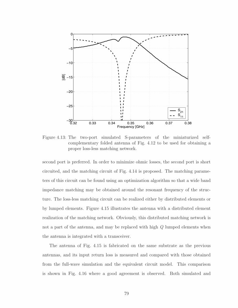
0.32 0.33 0.34 0.35 0.36 0.37 0.38−30
−25
−20
−15
−10
−5
0
Frequency [GHz]
[dB
]
S21
S11
Figure 4.13: The two-port simulated S-parameters of the miniaturized self-complementary folded antenna of Fig. 4.12 to be used for obtaining aproper loss-less matching network.
second port is preferred. In order to minimize ohmic losses, the second port is short
circuited, and the matching circuit of Fig. 4.14 is proposed. The matching parame-
ters of this circuit can be found using an optimization algorithm so that a wide band
impedance matching may be obtained around the resonant frequency of the struc-
ture. The loss-less matching circuit can be realized either by distributed elements or
by lumped elements. Figure 4.15 illustrates the antenna with a distributed element
realization of the matching network. Obviously, this distributed matching network is
not a part of the antenna, and may be replaced with high Q lumped elements when
the antenna is integrated with a transceiver.
The antenna of Fig. 4.15 is fabricated on the same substrate as the previous
antennas, and its input return loss is measured and compared with those obtained
from the full-wave simulation and the equivalent circuit model. This comparison
is shown in Fig. 4.16 where a good agreement is observed. Both simulated and
79
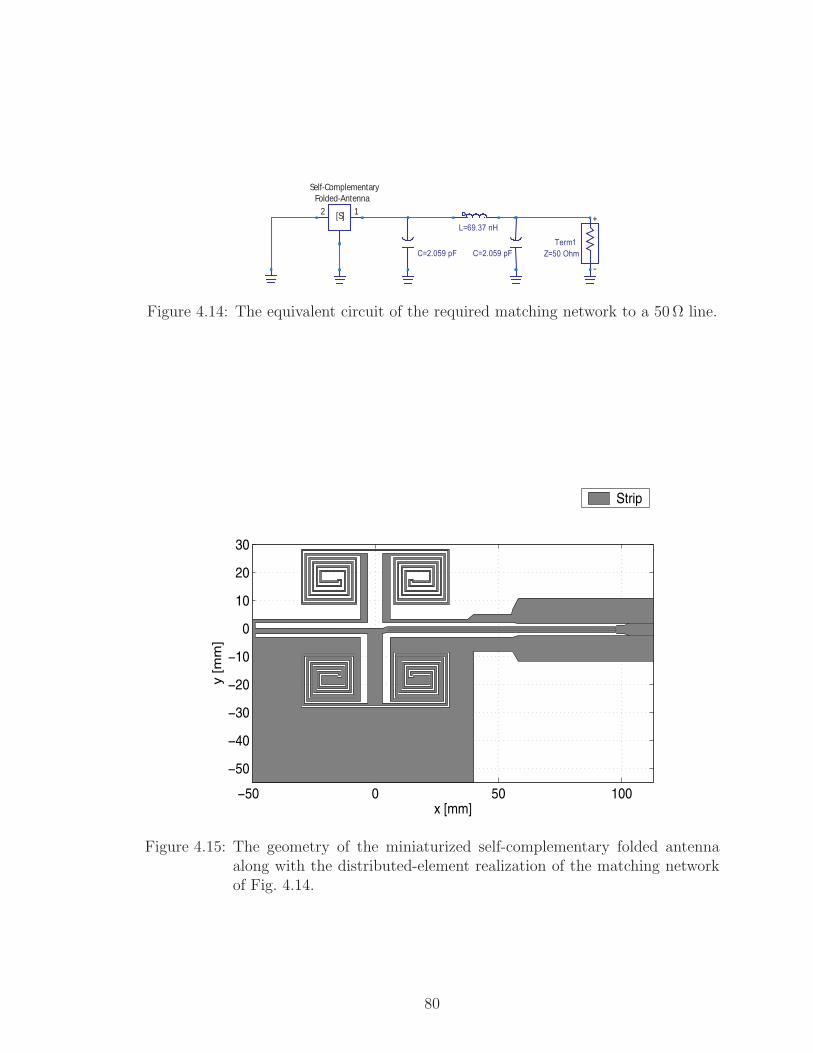
Term1Z=50 Ohm
L=69.37 nH
C=2.059 pFC=2.059 pF
+
-
[S]
Self-Complementary Folded-Antenna
2 1
Figure 4.14: The equivalent circuit of the required matching network to a 50 Ω line.
−50 0 50 100
−50
−40
−30
−20
−10
0
10
20
30
x [mm]
y [m
m]
Strip
Figure 4.15: The geometry of the miniaturized self-complementary folded antennaalong with the distributed-element realization of the matching networkof Fig. 4.14.
80
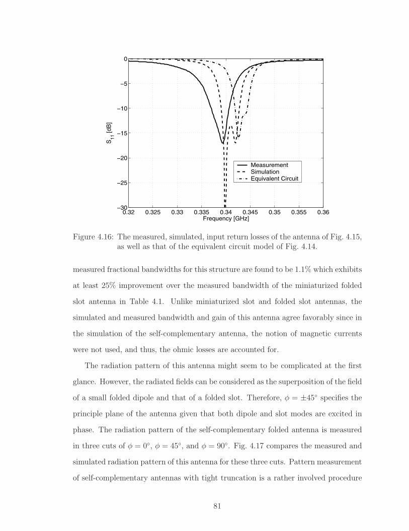
0.32 0.325 0.33 0.335 0.34 0.345 0.35 0.355 0.36−30
−25
−20
−15
−10
−5
0
Frequency [GHz]
S11
[dB
]
MeasurementSimulationEquivalent Circuit
Figure 4.16: The measured, simulated, input return losses of the antenna of Fig. 4.15,as well as that of the equivalent circuit model of Fig. 4.14.
measured fractional bandwidths for this structure are found to be 1.1% which exhibits
at least 25% improvement over the measured bandwidth of the miniaturized folded
slot antenna in Table 4.1. Unlike miniaturized slot and folded slot antennas, the
simulated and measured bandwidth and gain of this antenna agree favorably since in
the simulation of the self-complementary antenna, the notion of magnetic currents
were not used, and thus, the ohmic losses are accounted for.
The radiation pattern of this antenna might seem to be complicated at the first
glance. However, the radiated fields can be considered as the superposition of the field
of a small folded dipole and that of a folded slot. Therefore, φ = ±45 specifies the
principle plane of the antenna given that both dipole and slot modes are excited in
phase. The radiation pattern of the self-complementary folded antenna is measured
in three cuts of φ = 0, φ = 45, and φ = 90. Fig. 4.17 compares the measured and
simulated radiation pattern of this antenna for these three cuts. Pattern measurement
of self-complementary antennas with tight truncation is a rather involved procedure
81
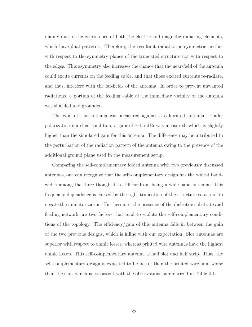
mainly due to the coexistence of both the electric and magnetic radiating elements,
which have dual patterns. Therefore, the resultant radiation is symmetric neither
with respect to the symmetry planes of the truncated structure nor with respect to
the edges. This asymmetry also increases the chance that the near-field of the antenna
could excite currents on the feeding cable, and that those excited currents re-radiate,
and thus, interfere with the far-fields of the antenna. In order to prevent unwanted
radiations, a portion of the feeding cable at the immediate vicinity of the antenna
was shielded and grounded.
The gain of this antenna was measured against a calibrated antenna. Under
polarization matched condition, a gain of −4.5 dBi was measured, which is slightly
higher than the simulated gain for this antenna. The difference may be attributed to
the perturbation of the radiation pattern of the antenna owing to the presence of the
additional ground plane used in the measurement setup.
Comparing the self-complementary folded antenna with two previously discussed
antennas, one can recognize that the self-complementary design has the widest band-
width among the three though it is still far from being a wide-band antenna. This
frequency dependence is caused by the tight truncation of the structure so as not to
negate the miniaturization. Furthermore, the presence of the dielectric substrate and
feeding network are two factors that tend to violate the self-complementary condi-
tions of the topology. The efficiency/gain of this antenna falls in between the gain
of the two previous designs, which is inline with our expectation. Slot antennas are
superior with respect to ohmic losses, whereas printed wire antennas have the highest
ohmic losses. This self-complementary antenna is half slot and half strip. Thus, the
self-complementary design is expected to be better than the printed wire, and worse
than the slot, which is consistent with the observations summarized in Table 4.1.
82
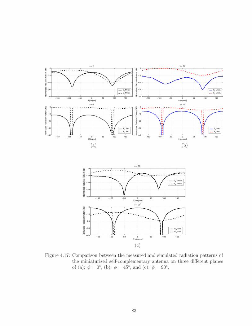
−150 −100 −50 0 50 100 150−40
−30
−20
−10
0
θ [degree]
Norm
aliz
ed R
adia
tion P
attern
[dB
]
φ = 0°
Eθ Meas.
Eφ Meas.
−150 −100 −50 0 50 100 150−40
−30
−20
−10
0
θ [degree]
Norm
aliz
ed R
adia
tion P
attern
[dB
]
φ = 0°
Eθ Sim.
Eφ Sim.
−150 −100 −50 0 50 100 150−40
−30
−20
−10
0
θ [degree]
Norm
aliz
ed R
adia
tion P
attern
[dB
]
φ = 45°
Eθ Meas.
Eφ Meas.
−150 −100 −50 0 50 100 150−40
−30
−20
−10
0
θ [degree]
Norm
aliz
ed R
adia
tion P
attern
[dB
]
φ = 45°
Eθ Sim.
Eφ Sim.
(a) (b)
−150 −100 −50 0 50 100 150−40
−30
−20
−10
0
θ [degree]
Nor
mal
ized
Rad
iatio
n P
atte
rn [d
B]
φ = 90°
Eθ Meas.
Eφ Meas.
−150 −100 −50 0 50 100 150−40
−30
−20
−10
0
θ [degree]
Nor
mal
ized
Rad
iatio
n P
atte
rn [d
B]
φ = 90°
Eθ Sim.
Eφ Sim.
(c)
Figure 4.17: Comparison between the measured and simulated radiation patterns ofthe miniaturized self-complementary antenna on three different planesof (a): φ = 0, (b): φ = 45, and (c): φ = 90.
83

4.5 Self-Complimentary H-Shaped Antenna
In the self-complementary antenna design of the previous section, the main ob-
jective was to maintain a very small size, regardless of how adversely the required
conditions for self-complementary structures were affected. In this section, a more
compatible design with the self-complementary conditions is introduced. In this de-
sign, the miniaturization criterion is relaxed by reducing the end-loading. By remov-
ing all of the loading spiral arms except for one, an H-antenna is obtained. Figure 4.18
shows the geometry of this structure fed by a short-circuited microstrip line. Note
that a via-hole connects the end of the microstrip line of Fig. 4.18 to the right hand
side of the ground plane. Again a substrate with εr = 2.2 and a thickness of 0.787 mm
was used to fabricate this antenna. An impedance step in the microstrip line, as well
as two short stubs, was introduced to enhance the impedance matching to a 50 Ω
line. The simulated and measured input return losses of this antenna are illustrated
in Fig. 4.19. As shown in this figure, a very wide −10 dB bandwidth from 1.35 GHz
to 3.2 GHz (2.3:1) is achieved. To demonstrate the effect of the substrate in per-
turbing the self-complementarity, the same structure is simulated with no dielectric
substrate (εr = 1.0) as well. The simulated return loss of this antenna is also il-
lustrated in Fig. 4.19, where it demonstrates a considerably wider bandwidth from
1.3 GHz to 3.9 GHz (3:1).
Another source of frequency dependance in the response of the antenna structure
in Fig. 4.18 is the asymmetry created by the microstrip feed and the corresponding
matching network. Comparing this feeding configuration with those of the perfectly
self-complementary structures [38, 39], one can recognize that the symmetry can only
be preserved when the antenna structure has two ports, and the second port is ter-
minated by a resistance of RL = Z0/2 = 60π Ω. Using this terminated configuration,
the input impedance of the antenna becomes 60π = 188 Ω over a wide frequency
band requiring an additional wide-band matching network, should the antenna be
84
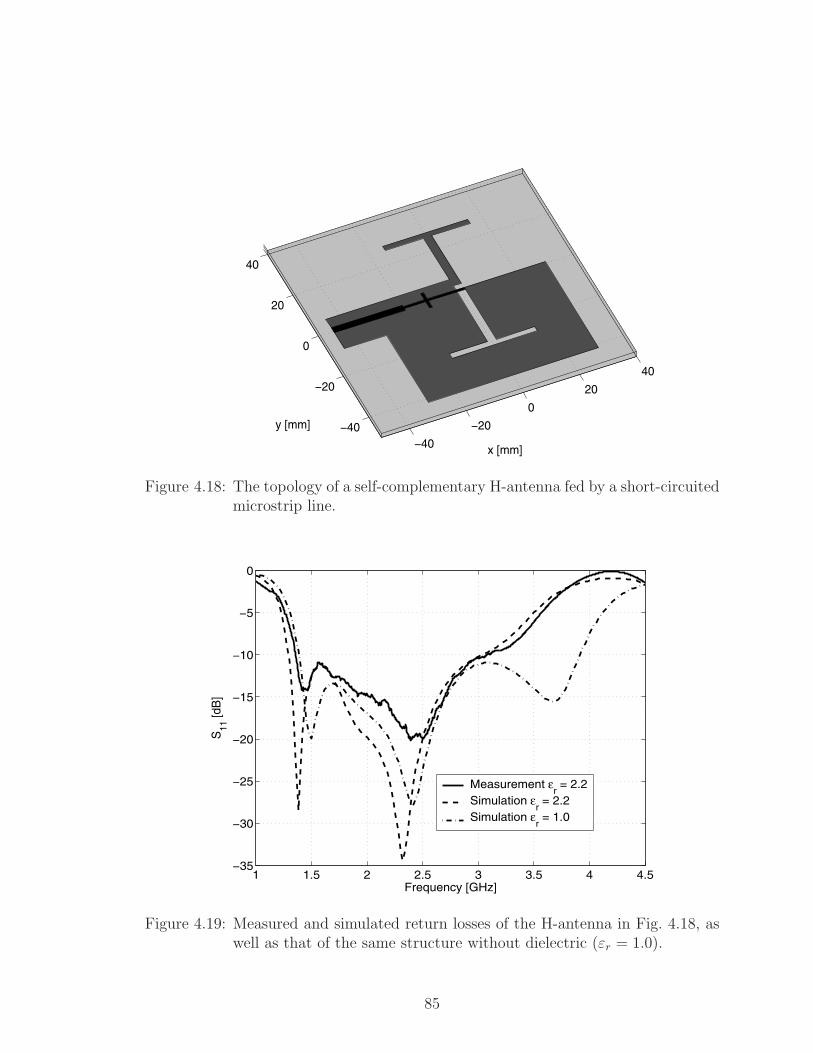
−40
−20
0
20
40
−40
−20
0
20
40
x [mm]
y [mm]
Figure 4.18: The topology of a self-complementary H-antenna fed by a short-circuitedmicrostrip line.
1 1.5 2 2.5 3 3.5 4 4.5−35
−30
−25
−20
−15
−10
−5
0
Frequency [GHz]
S11
[dB
]
Measurement εr = 2.2
Simulation εr = 2.2
Simulation εr = 1.0
Figure 4.19: Measured and simulated return losses of the H-antenna in Fig. 4.18, aswell as that of the same structure without dielectric (εr = 1.0).
85
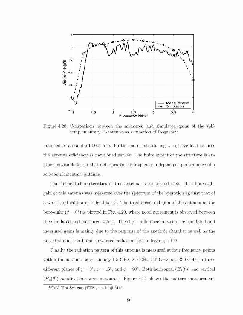
1 1.5 2 2.5 3 3.5 4−8
−6
−4
−2
0
2
4
Frequency [GHz]
Ante
nna
Gai
n [d
Bi]
MeasurementSimulation
Figure 4.20: Comparison between the measured and simulated gains of the self-complementary H-antenna as a function of frequency.
matched to a standard 50 Ω line. Furthermore, introducing a resistive load reduces
the antenna efficiency as mentioned earlier. The finite extent of the structure is an-
other inevitable factor that deteriorates the frequency-independent performance of a
self-complementary antenna.
The far-field characteristics of this antenna is considered next. The bore-sight
gain of this antenna was measured over the spectrum of the operation against that of
a wide band calibrated ridged horn1. The total measured gain of the antenna at the
bore-sight (θ = 0) is plotted in Fig. 4.20, where good agreement is observed between
the simulated and measured values. The slight difference between the simulated and
measured gains is mainly due to the response of the anechoic chamber as well as the
potential multi-path and unwanted radiation by the feeding cable.
Finally, the radiation pattern of this antenna is measured at four frequency points
within the antenna band, namely 1.5 GHz, 2.0 GHz, 2.5 GHz, and 3.0 GHz, in three
different planes of φ = 0, φ = 45, and φ = 90. Both horizontal (Eθ(θ)) and vertical
(Eφ(θ)) polarizations were measured. Figure 4.21 shows the pattern measurement
1EMC Test Systems (ETS), model # 3115
86
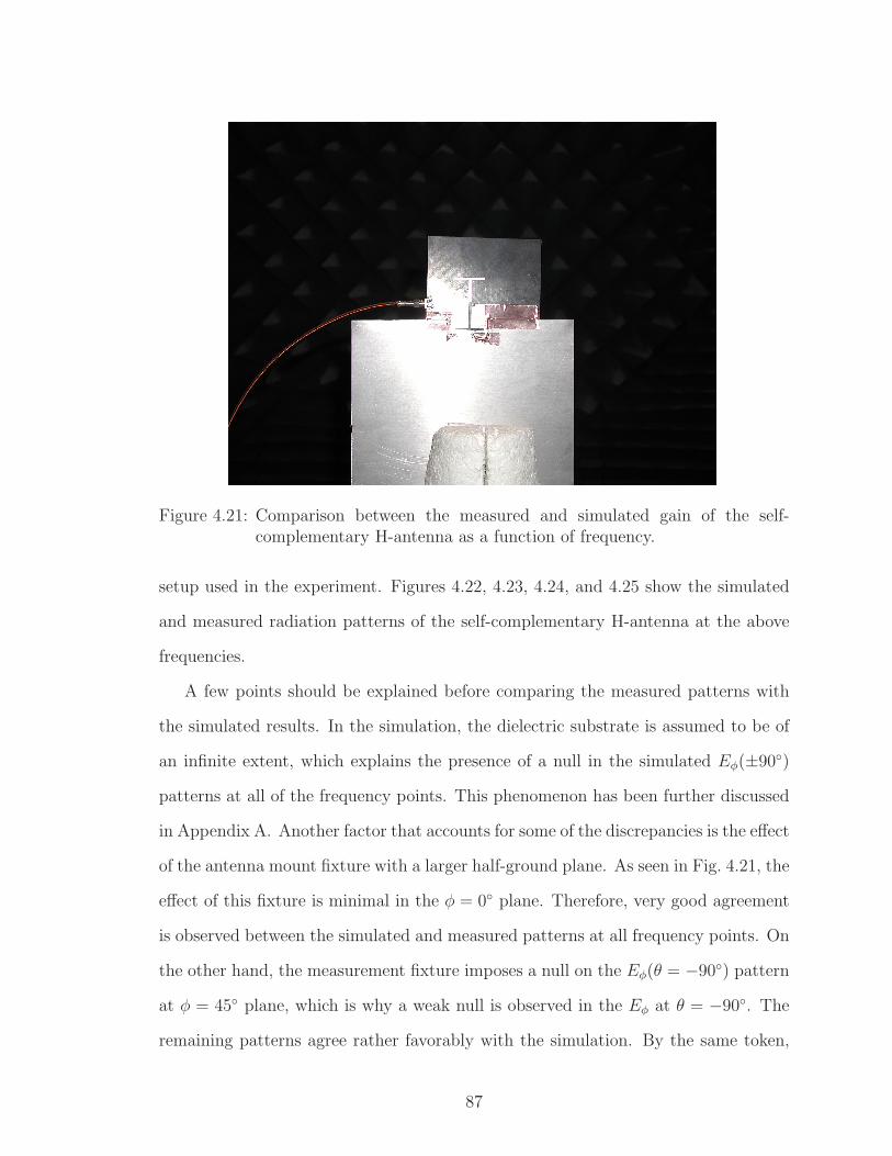
Figure 4.21: Comparison between the measured and simulated gain of the self-complementary H-antenna as a function of frequency.
setup used in the experiment. Figures 4.22, 4.23, 4.24, and 4.25 show the simulated
and measured radiation patterns of the self-complementary H-antenna at the above
frequencies.
A few points should be explained before comparing the measured patterns with
the simulated results. In the simulation, the dielectric substrate is assumed to be of
an infinite extent, which explains the presence of a null in the simulated Eφ(±90)
patterns at all of the frequency points. This phenomenon has been further discussed
in Appendix A. Another factor that accounts for some of the discrepancies is the effect
of the antenna mount fixture with a larger half-ground plane. As seen in Fig. 4.21, the
effect of this fixture is minimal in the φ = 0 plane. Therefore, very good agreement
is observed between the simulated and measured patterns at all frequency points. On
the other hand, the measurement fixture imposes a null on the Eφ(θ = −90) pattern
at φ = 45 plane, which is why a weak null is observed in the Eφ at θ = −90. The
remaining patterns agree rather favorably with the simulation. By the same token,
87
−20dB
−10dB
0dB
30
210
60
240
90
270
120
300
150
330
180 0
φ = 0°
θ [d
egre
e]
EφEθ
−20dB
−10dB
0dB
30
210
60
240
90
270
120
300
150
330
180 0
φ = 45°
θ [d
egre
e]
EφEθ
−20dB
−10dB
0dB
30
210
60
240
90
270
120
300
150
330
180 0
φ = 90°
θ [d
egre
e]
EφEθ
(a)
−20dB
−10dB
0dB
30
210
60
240
90
270
120
300
150
330
180 0
φ = 0°
θ [d
egre
e]
EφEθ
−20dB
−10dB
0dB
30
210
60
240
90
270
120
300
150
330
180 0
φ = 45°
θ [d
egre
e]
EφEθ
−20dB
−10dB
0dB
30
210
60
240
90
270
120
300
150
330
180 0
φ = 90°
θ [d
egre
e]
EφEθ
(b)
Figure 4.22: Comparison between the measured and simulated radiation patterns ofthe self-complementary H antenna at 1.5 GHz for three cuts of φ = 0,φ = 45, φ = 90; (a): measurements, (b): simulations.
88
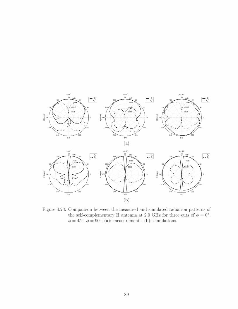
−30dB
−20dB
−10dB
0dB
30
210
60
240
90
270
120
300
150
330
180 0
φ = 0°
θ [d
egre
e]
EφEθ
−30dB
−20dB
−10dB
0dB
30
210
60
240
90
270
120
300
150
330
180 0
φ = 45°
θ [d
egre
e]
EφEθ
−30dB
−20dB
−10dB
0dB
30
210
60
240
90
270
120
300
150
330
180 0
φ = 90°
θ [d
egre
e]
EφEθ
(a)
−20dB
−10dB
0dB
30
210
60
240
90
270
120
300
150
330
180 0
φ = 0°
θ [d
egre
e]
EφEθ
−20dB
−10dB
0dB
30
210
60
240
90
270
120
300
150
330
180 0
φ = 45°
θ [d
egre
e]
EφEθ
−20dB
−10dB
0dB
30
210
60
240
90
270
120
300
150
330
180 0
φ = 90°
θ [d
egre
e]
EφEθ
(b)
Figure 4.23: Comparison between the measured and simulated radiation patterns ofthe self-complementary H antenna at 2.0 GHz for three cuts of φ = 0,φ = 45, φ = 90; (a): measurements, (b): simulations.
89
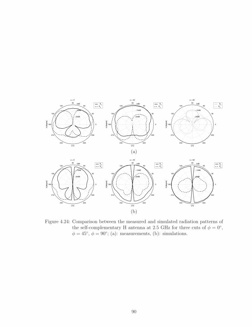
−20dB
−10dB
0dB
30
210
60
240
90
270
120
300
150
330
180 0
φ = 0°
θ [d
egre
e]
EφEθ
−20dB
−10dB
0dB
30
210
60
240
90
270
120
300
150
330
180 0
φ = 45°
θ [d
egre
e]
EφEθ
−20dB
−10dB
0dB
30
210
60
240
90
270
120
300
150
330
180 0
φ = 90°
θ [d
egre
e]
EφEθ
(a)
−20dB
−10dB
0dB
30
210
60
240
90
270
120
300
150
330
180 0
φ = 0°
θ [d
egre
e]
EφEθ
−20dB
−10dB
0dB
30
210
60
240
90
270
120
300
150
330
180 0
φ = 45°
θ [d
egre
e]
EφEθ
−20dB
−10dB
0dB
30
210
60
240
90
270
120
300
150
330
180 0
φ = 90°
θ [d
egre
e]
EφEθ
(b)
Figure 4.24: Comparison between the measured and simulated radiation patterns ofthe self-complementary H antenna at 2.5 GHz for three cuts of φ = 0,φ = 45, φ = 90; (a): measurements, (b): simulations.
90
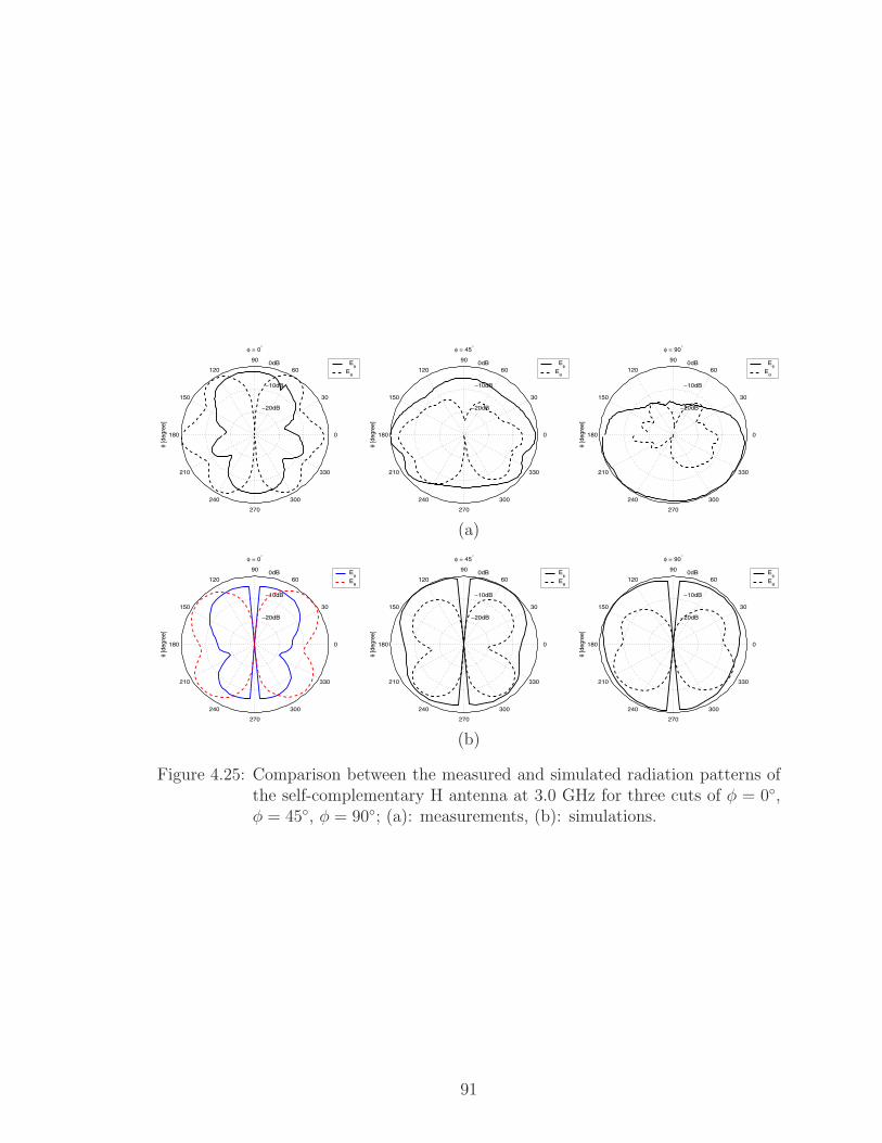
−20dB
−10dB
0dB
30
210
60
240
90
270
120
300
150
330
180 0
φ = 0°
θ [d
egre
e]
EφEθ
−20dB
−10dB
0dB
30
210
60
240
90
270
120
300
150
330
180 0
φ = 45°
θ [d
egre
e]
EφEθ
−20dB
−10dB
0dB
30
210
60
240
90
270
120
300
150
330
180 0
φ = 90°
θ [d
egre
e]
EφEθ
(a)
−20dB
−10dB
0dB
30
210
60
240
90
270
120
300
150
330
180 0
φ = 0°
θ [d
egre
e]
EφEθ
−20dB
−10dB
0dB
30
210
60
240
90
270
120
300
150
330
180 0
φ = 45°
θ [d
egre
e]
EφEθ
−20dB
−10dB
0dB
30
210
60
240
90
270
120
300
150
330
180 0
φ = 90°
θ [d
egre
e]
EφEθ
(b)
Figure 4.25: Comparison between the measured and simulated radiation patterns ofthe self-complementary H antenna at 3.0 GHz for three cuts of φ = 0,φ = 45, φ = 90; (a): measurements, (b): simulations.
91
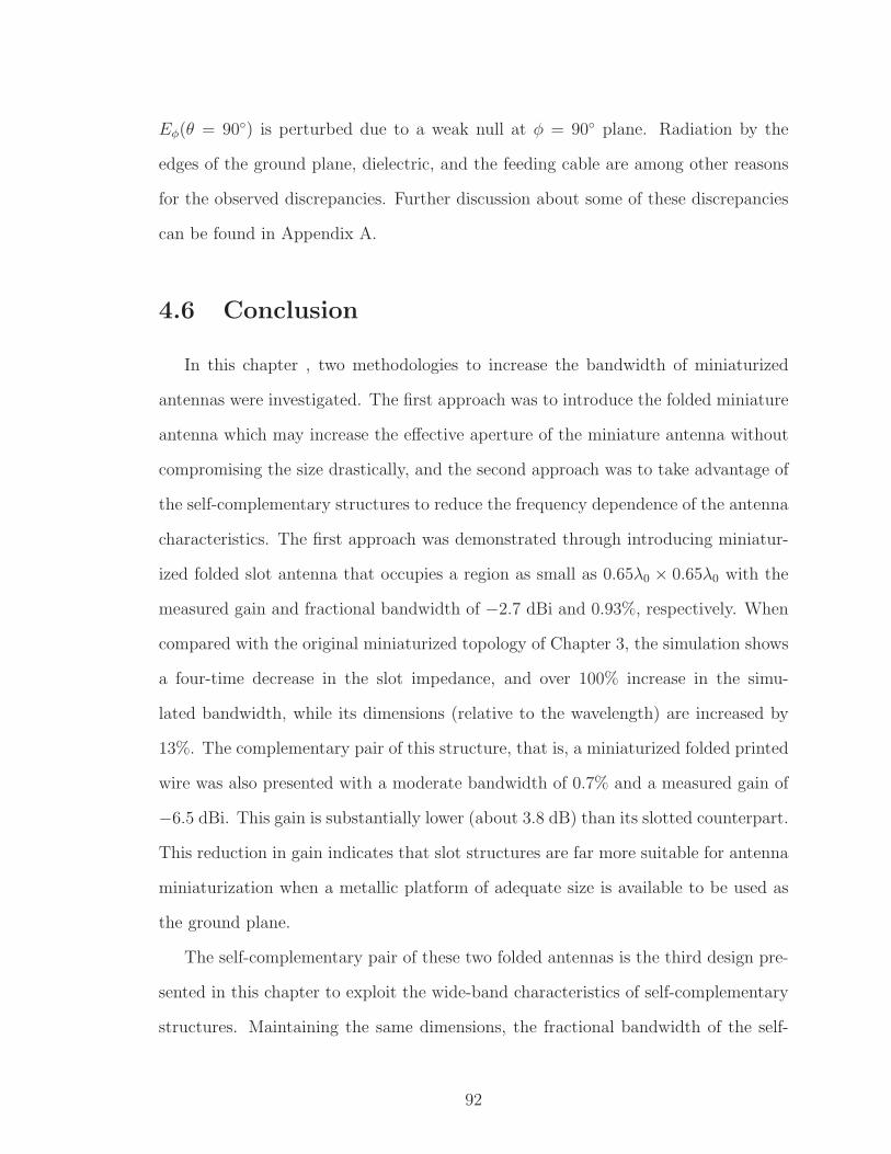
Eφ(θ = 90) is perturbed due to a weak null at φ = 90 plane. Radiation by the
edges of the ground plane, dielectric, and the feeding cable are among other reasons
for the observed discrepancies. Further discussion about some of these discrepancies
can be found in Appendix A.
4.6 Conclusion
In this chapter , two methodologies to increase the bandwidth of miniaturized
antennas were investigated. The first approach was to introduce the folded miniature
antenna which may increase the effective aperture of the miniature antenna without
compromising the size drastically, and the second approach was to take advantage of
the self-complementary structures to reduce the frequency dependence of the antenna
characteristics. The first approach was demonstrated through introducing miniatur-
ized folded slot antenna that occupies a region as small as 0.65λ0 × 0.65λ0 with the
measured gain and fractional bandwidth of −2.7 dBi and 0.93%, respectively. When
compared with the original miniaturized topology of Chapter 3, the simulation shows
a four-time decrease in the slot impedance, and over 100% increase in the simu-
lated bandwidth, while its dimensions (relative to the wavelength) are increased by
13%. The complementary pair of this structure, that is, a miniaturized folded printed
wire was also presented with a moderate bandwidth of 0.7% and a measured gain of
−6.5 dBi. This gain is substantially lower (about 3.8 dB) than its slotted counterpart.
This reduction in gain indicates that slot structures are far more suitable for antenna
miniaturization when a metallic platform of adequate size is available to be used as
the ground plane.
The self-complementary pair of these two folded antennas is the third design pre-
sented in this chapter to exploit the wide-band characteristics of self-complementary
structures. Maintaining the same dimensions, the fractional bandwidth of the self-
92
complementary antenna reaches to 1.1%, which exhibits at least 25% increase over
its slotted and printed strip counterparts. The gain/efficiency of this antenna, as ex-
pected, falls between those of the folded slot and printed wire antennas. When minia-
turization criterion is relaxed in exchange for satisfying more of the self-complementarity
conditions, a much wider bandwidth can be obtained, an example of which is an H-
antenna. This antenna demonstrates a very wide −10 dB return loss bandwidth of
2.3:1 and a fairly constant gain of slightly above 1 dBi over the entire frequency
band of operation. The dimensions of this antenna are 0.13λ0 × 0.24λ0 at the lowest
frequency of operation (1.3 GHz).
93
CHAPTER 5
RF Filter Miniaturization Using a High-Q
Slot-line Resonator
5.1 Introduction
Mobile wireless systems of various kinds, e.g., cellular phones, hand-held GPS
units, and palm pilots have become an integral part of everyday life. Future expan-
sion of the wireless market depends on the cost, size, and power efficiency of the
wireless systems. These characteristics are the driving force behind substantial re-
search efforts towards miniaturizing the RF frontend of wireless devices. High-Q low
insertion loss miniaturized filters, with applications in multiplexer and co-site inter-
ference suppression, are important components of the RF frontend. A few approaches
in the literature address filter miniaturization, among which are the use of lumped-
element filters, high-temperature super-conducting (HTS) filters, bulk acoustic-wave
(BAW) filters, and slow-wave distributed resonator filters [5, 6, 7, 40].
Lumped-element filters can be made very small at lower frequencies. At higher
frequencies, however, their extremely small size may result in high insertion loss and
possibly low power handling capacity. To cope with the insertion loss problem, high-
temperature super-conducting filters (HTS) have been proposed. BAW filters also
94

have exceptionally small size and fairly good performance but may be extremely ex-
pensive to develop for any new application. These two classes of filters are not further
considered in this chapter, the subject of which is to introduce a new type of high-Q
coiled slot-line resonator with comparison to the microstrip. On the other hand, con-
ventional distributed element filters using coupled transmission line resonators exhibit
superior performance but are frequently too large.
In order to reach a compromise between size and performance, some compact
architectures have been proposed. The size reduction of ordinary microstrip line
resonators, for example, was made possible first by employing microstrip stepped
impedance resonators (SIR) [41, 42], and then, by using hairpin-line resonators [43].
A more compact hairpin filter using split ring resonators with parallel coupled lines
was later proposed [44]. This resonator is a capacitively end-loaded hairpin resonator
where the loading is implemented by distributed coupled lines. The loaded hairpin
resonator, together with the SIR, resulted in an improved hairpin resonator [45].
Incorporating dissimilar resonators in filter design has also been reported [45].
Another form of resonator which is similar to the above hairpin resonators uti-
lizes square open loops [46]. To further reduce size, the open loop structure can be
modified by introducing a narrow capacitive gap at the open end of the loop [47].
The same authors suggested an aperture coupled two-layer filter design using the
same type of resonator [48]. Using the two sides of the substrate provides additional
miniaturization. In both loaded open loop and loaded hairpin resonators, electric and
magnetic coupling can be implemented, which allows for the flexible design of many
structures, such as quasi-elliptic filters.
Slot-lines and coplanar waveguides (CPW) are other important configurations for
the realization of resonators and filters. In the early 1970s, slot transmission lines
were shown to be a practical configuration for the realization of microwave filters
and couplers [49], but more attention has been devoted to CPW filters [26, 50, 51].
95
Also known as uniplanar configurations, slot and CPW lines are fundamental to
many microwave and millimeter-wave integrated circuits [52, 53]. With regard to
CPW filter miniaturization, the use of quarter-wave transmission line resonators, for
example a λ/4 CPW hairpin resonator [54], meandered super-conducting CPW filters
[55], double surface CPW filters [56], and air bridge capacitive loadings have been
proposed. Additionally, the periodic loading of CPW lines has been suggested to
construct a slow wave transmission line and used in the fabrication of a miniature
low pass filter [57].
In contrast, the literature concerning the use of slot-lines for filter design and filter
miniaturization is rather scarce. The Q of slot-line resonators is higher than that of
microstrip resonators of similar dimensions due to the fact that the stored energy
in the resonator is confined within a larger volume, and that the electric current
flows over a wider area, which translates into lower ohmic losses. Actually, slot-lines
are comparable to suspended substrate strip-lines, which also have higher Q than
microstrips due to the larger volume occupied by the stored energy.
In this chapter, a new class of low insertion loss miniaturized filters using slot-line
resonators is proposed. Miniaturization is achieved by terminating the slot-line with a
double-spiral inductive termination at both ends. Using this miniaturized resonator,
both positive and negative couplings may be realized by appropriate geometric lay-
out of the miniaturized resonators, and therefore, both standard coupled-line and
cross-coupled quasi-elliptic filters are realizable. The unloaded Q of these slot-line
filters is considerably higher than that of miniaturized microstrip filters of compara-
ble dimensions due to the inherent higher Q of slot-line. To demonstrate the validity
of the design procedures and the performance characteristics, two different types of
filters were fabricated and tested. One is a four-pole Chebyshev filter, and the other
is a quasi-elliptic filter, where in each case the full-wave simulations show very good
agreement with measurements.
96
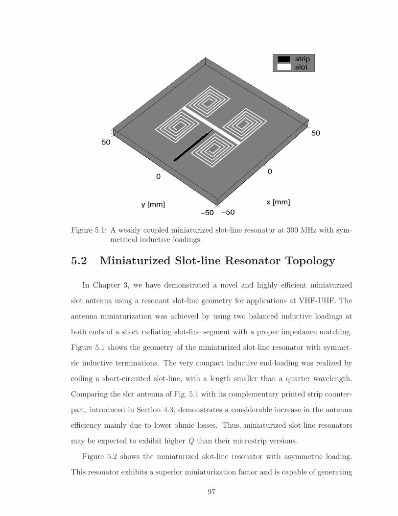
−50
0
50
−50
0
50
y [mm] x [mm]
stripslot
Figure 5.1: A weakly coupled miniaturized slot-line resonator at 300 MHz with sym-metrical inductive loadings.
5.2 Miniaturized Slot-line Resonator Topology
In Chapter 3, we have demonstrated a novel and highly efficient miniaturized
slot antenna using a resonant slot-line geometry for applications at VHF-UHF. The
antenna miniaturization was achieved by using two balanced inductive loadings at
both ends of a short radiating slot-line segment with a proper impedance matching.
Figure 5.1 shows the geometry of the miniaturized slot-line resonator with symmet-
ric inductive terminations. The very compact inductive end-loading was realized by
coiling a short-circuited slot-line, with a length smaller than a quarter wavelength.
Comparing the slot antenna of Fig. 5.1 with its complementary printed strip counter-
part, introduced in Section 4.3, demonstrates a considerable increase in the antenna
efficiency mainly due to lower ohmic losses. Thus, miniaturized slot-line resonators
may be expected to exhibit higher Q than their microstrip versions.
Figure 5.2 shows the miniaturized slot-line resonator with asymmetric loading.
This resonator exhibits a superior miniaturization factor and is capable of generating
97
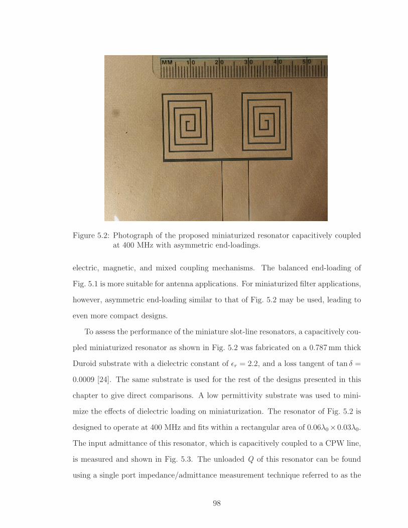
Figure 5.2: Photograph of the proposed miniaturized resonator capacitively coupledat 400 MHz with asymmetric end-loadings.
electric, magnetic, and mixed coupling mechanisms. The balanced end-loading of
Fig. 5.1 is more suitable for antenna applications. For miniaturized filter applications,
however, asymmetric end-loading similar to that of Fig. 5.2 may be used, leading to
even more compact designs.
To assess the performance of the miniature slot-line resonators, a capacitively cou-
pled miniaturized resonator as shown in Fig. 5.2 was fabricated on a 0.787 mm thick
Duroid substrate with a dielectric constant of εr = 2.2, and a loss tangent of tan δ =
0.0009 [24]. The same substrate is used for the rest of the designs presented in this
chapter to give direct comparisons. A low permittivity substrate was used to mini-
mize the effects of dielectric loading on miniaturization. The resonator of Fig. 5.2 is
designed to operate at 400 MHz and fits within a rectangular area of 0.06λ0 ×0.03λ0.
The input admittance of this resonator, which is capacitively coupled to a CPW line,
is measured and shown in Fig. 5.3. The unloaded Q of this resonator can be found
using a single port impedance/admittance measurement technique referred to as the
98
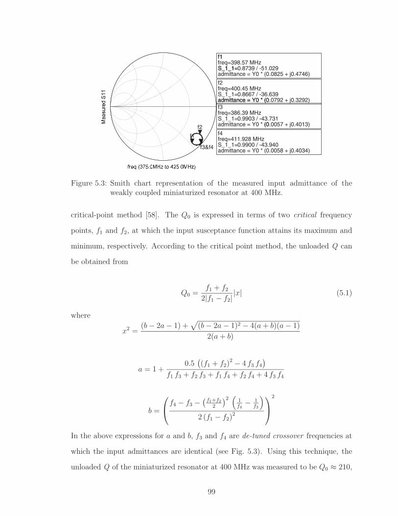
f1freq=398.57 MHzS_1_1=0.8739 / -51.029admittance = Y0 * (0.0825 + j0.4746)
f2freq=400.45 MHzS_1_1=0.8667 / -36.639admittance = Y0 * (0.0792 + j0.3292)f3freq=386.39 MHzS_1_1=0.9903 / -43.731admittance = Y0 * (0.0057 + j0.4013)
f4freq=411.928 MHzS_1_1=0.9900 / -43.940admittance = Y0 * (0.0058 + j0.4034)
f1
S_1_1=
admittance = Y0 * (0
(0
f1
f2
f3&f4
Figure 5.3: Smith chart representation of the measured input admittance of theweakly coupled miniaturized resonator at 400 MHz.
critical-point method [58]. The Q0 is expressed in terms of two critical frequency
points, f1 and f2, at which the input susceptance function attains its maximum and
minimum, respectively. According to the critical point method, the unloaded Q can
be obtained from
Q0 =f1 + f2
2|f1 − f2| |x| (5.1)
where
x2 =(b − 2a − 1) +
√(b − 2a − 1)2 − 4(a + b)(a − 1)
2(a + b)
a = 1 +0.5
((f1 + f2)
2 − 4 f3 f4
)f1 f3 + f2 f3 + f1 f4 + f2 f4 + 4 f3 f4
b =
f4 − f3 −
(f1+f2
2
)2(
1f4
− 1f3
)
2 (f1 − f2)2
2
In the above expressions for a and b, f3 and f4 are de-tuned crossover frequencies at
which the input admittances are identical (see Fig. 5.3). Using this technique, the
unloaded Q of the miniaturized resonator at 400 MHz was measured to be Q0 ≈ 210,
99
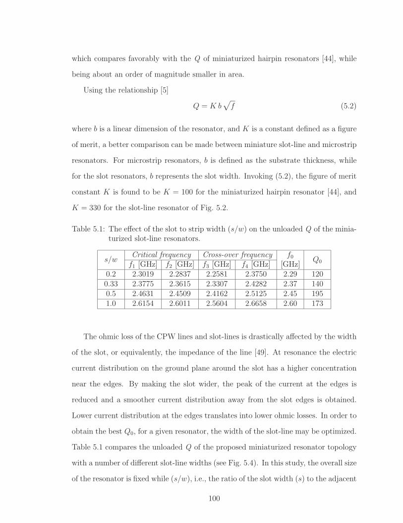
which compares favorably with the Q of miniaturized hairpin resonators [44], while
being about an order of magnitude smaller in area.
Using the relationship [5]
Q = K b√
f (5.2)
where b is a linear dimension of the resonator, and K is a constant defined as a figure
of merit, a better comparison can be made between miniature slot-line and microstrip
resonators. For microstrip resonators, b is defined as the substrate thickness, while
for the slot resonators, b represents the slot width. Invoking (5.2), the figure of merit
constant K is found to be K = 100 for the miniaturized hairpin resonator [44], and
K = 330 for the slot-line resonator of Fig. 5.2.
Table 5.1: The effect of the slot to strip width (s/w) on the unloaded Q of the minia-turized slot-line resonators.
s/wCritical frequency Cross-over frequency f0
[GHz]Q0f1 [GHz] f2 [GHz] f3 [GHz] f4 [GHz]
0.2 2.3019 2.2837 2.2581 2.3750 2.29 1200.33 2.3775 2.3615 2.3307 2.4282 2.37 1400.5 2.4631 2.4509 2.4162 2.5125 2.45 1951.0 2.6154 2.6011 2.5604 2.6658 2.60 173
The ohmic loss of the CPW lines and slot-lines is drastically affected by the width
of the slot, or equivalently, the impedance of the line [49]. At resonance the electric
current distribution on the ground plane around the slot has a higher concentration
near the edges. By making the slot wider, the peak of the current at the edges is
reduced and a smoother current distribution away from the slot edges is obtained.
Lower current distribution at the edges translates into lower ohmic losses. In order to
obtain the best Q0, for a given resonator, the width of the slot-line may be optimized.
Table 5.1 compares the unloaded Q of the proposed miniaturized resonator topology
with a number of different slot-line widths (see Fig. 5.4). In this study, the overall size
of the resonator is fixed while (s/w), i.e., the ratio of the slot width (s) to the adjacent
100
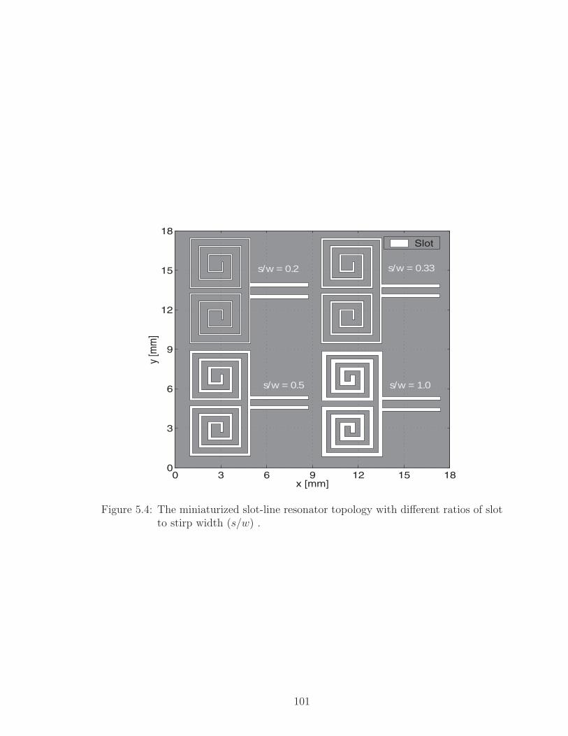
0 3 6 9 12 15 180
3
6
9
12
15
18
x [mm]
y [m
m]
Slot
s/w = 0.2 s/w = 0.33
s/w = 0.5 s/w = 1.0
Figure 5.4: The miniaturized slot-line resonator topology with different ratios of slotto stirp width (s/w) .
101
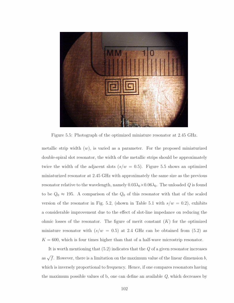
Figure 5.5: Photograph of the optimized miniature resonator at 2.45 GHz.
metallic strip width (w), is varied as a parameter. For the proposed miniaturized
double-spiral slot resonator, the width of the metallic strips should be approximately
twice the width of the adjacent slots (s/w = 0.5). Figure 5.5 shows an optimized
miniaturized resonator at 2.45 GHz with approximately the same size as the previous
resonator relative to the wavelength, namely 0.03λ0×0.06λ0. The unloaded Q is found
to be Q0 ≈ 195. A comparison of the Q0 of this resonator with that of the scaled
version of the resonator in Fig. 5.2, (shown in Table 5.1 with s/w = 0.2), exhibits
a considerable improvement due to the effect of slot-line impedance on reducing the
ohmic losses of the resonator. The figure of merit constant (K) for the optimized
miniature resonator with (s/w = 0.5) at 2.4 GHz can be obtained from (5.2) as
K = 600, which is four times higher than that of a half-wave microstrip resonator.
It is worth mentioning that (5.2) indicates that the Q of a given resonator increases
as√
f . However, there is a limitation on the maximum value of the linear dimension b,
which is inversely proportional to frequency. Hence, if one compares resonators having
the maximum possible values of b, one can define an available Q, which decreases by
102
the square root of frequency.
To measure the radiation loss of the resonator, it was enclosed in a larger metallic
cavity and its Q was measured to be Q′0 = 265. Therefore, the Q due to the radiation
loss can be obtained from
1
Qrad
=1
Q0
− 1
Q′0
(5.3)
giving Qrad ≈ 808. This result indicates that the Q of the resonator is dominated by
the ohmic and dielectric losses.
In this section, only measurement has been used to identify the quality factor of the
proposed resonators since a numerical estimate of Q for the miniaturized resonators
does not provide very accurate results. For example, the finite element method (FEM)
requires enormous amounts of memory and extremely small cell sizes due to the very
large ratio of fine and coarse features of the structure. On the other hand, full-
wave methods based on integral equations (Method of Moments) make use of the
Green’s Function for multi-layer structures of infinite extent. Hence, ground planes
and substrates of finite size cannot be modelled efficiently. The equivalent magnetic
current method, however, provides a numerically efficient approach for the simulation
of slotted structures. In this approach, the tangential electric field over the slot is
replaced with an equivalent magnetic current, while the field is assumed to vanish
over the ground plane. This assumption implies that the ground plane is a perfect
conductor, and therefore, the ohmic loss cannot be modelled in this case. Obviously,
the ground plane of the slot-line resonators under study is neither a perfect conductor
nor is it extended to infinity. Despite the aforementioned drawbacks of the integral
equation method, such as [25], it can predict the frequency response of the filters very
accurately with the exception of the insertion-loss.
103

5.3 Direct-Coupled 4-Pole Filter
To demonstrate the versatility of the proposed miniaturized resonators to design
different types of filters, we begin with the design of direct-coupled bandpass filters.
A bandpass filter may be characterized by a set of internally coupled resonators (not
necessarily identical) all resonating at the same frequency, and an external quality
factor denoting the input and output couplings. The couplings between resonator
pairs and the input/output coupling are represented by kij and Qext, respectively. In
what follows, the coupling architectures as well as external coupling mechanisms are
investigated.
5.3.1 Coupling Structures
For the case of capacitively coupled miniaturized slot resonators, the resonators
have a series equivalent circuit model. Figure 5.6 illustrates the equivalent circuit
of two coupled miniaturized resonators exhibiting electric, magnetic, and mixed cou-
plings all realized by impedance (K) inverter.
In order to realize the desired values for the coupling coefficients, there are different
coupling configurations. In each of these configurations, the coupling coefficients
may be extracted using the pole splitting method [46] in conjunction with full-wave
simulations [25]. In the pole splitting method, a relationship is established between
the frequency separation of the poles and the coupling coefficients, as well as the
corresponding coupling capacitance or inductance in the impedance inverter. Given
that fu and fl are the frequencies at which the S21 reaches its peak values, the coupling
coefficients can be obtained from
k =f 2
u − f 2l
f 2u + f 2
l
. (5.4)
In the case of the pure electric or magnetic coupling whose appropriate circuit models
104
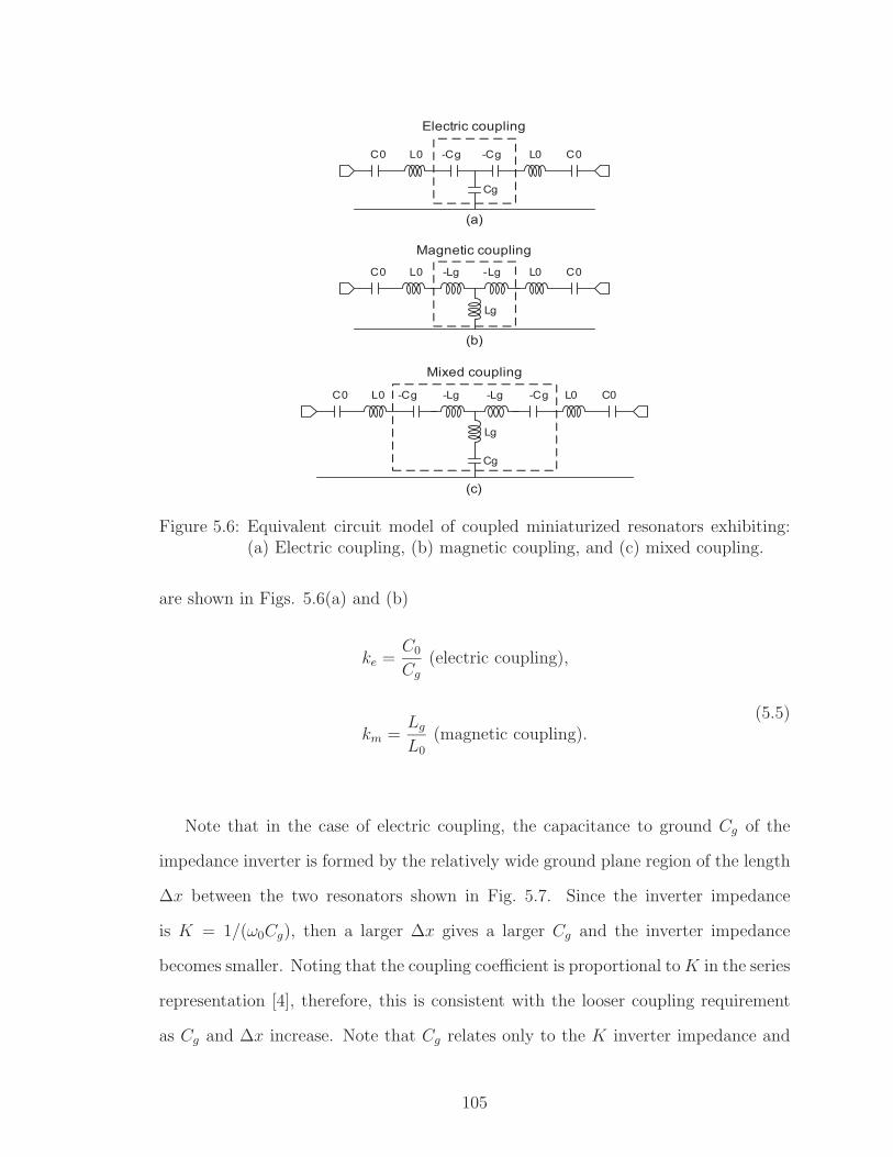
Electric coupling
(a)
L0 C0L0C0 -Cg
Cg
-Cg
Magnetic coupling
(b)
Lg
L0 C0L0C0 -Lg -Lg
Mixed coupling
(c)
Lg
L0C0 -Lg-Cg
Cg
L0 C0-Lg -Cg
Figure 5.6: Equivalent circuit model of coupled miniaturized resonators exhibiting:(a) Electric coupling, (b) magnetic coupling, and (c) mixed coupling.
are shown in Figs. 5.6(a) and (b)
ke =C0
Cg
(electric coupling),
km =Lg
L0
(magnetic coupling).(5.5)
Note that in the case of electric coupling, the capacitance to ground Cg of the
impedance inverter is formed by the relatively wide ground plane region of the length
∆x between the two resonators shown in Fig. 5.7. Since the inverter impedance
is K = 1/(ω0Cg), then a larger ∆x gives a larger Cg and the inverter impedance
becomes smaller. Noting that the coupling coefficient is proportional to K in the series
representation [4], therefore, this is consistent with the looser coupling requirement
as Cg and ∆x increase. Note that Cg relates only to the K inverter impedance and
105
is unrelated to the mutual capacitance between the resonators.
Mixed coupling may also be represented by an impedance invertor as shown in
Fig. 5.6(c). Since usually C0 Cg and Lg L0, the coupling coefficient for the
mixed coupling can be simplified as
kem =L0C0 − LgCg
LgC0 − L0Cg
≈ Lg
L0
− C0
Cg
= km − ke (5.6)
Equation (5.6) indicates that, for mixed coupling, the electric and magnetic coupling
are out of phase and tend to counteract each other. Examining the mixed coupling
more closely, it becomes clear that at the frequency of ωn = 1/√
Lg Cg, the two
resonators in Fig. 5.6(c) become decoupled, and a zero in the pass-band is introduced.
For dominant electric coupling where ke > km,
1
Cgω0
> ω0Lg =⇒ ωn > ω0 =1√
L0C0
(5.7)
Likewise, when the magnetic coupling is dominant, the zero appears below the pass-
band, that is ωn < ω0 .
In order to design the first Chebyshev prototype, two different coupling configu-
rations are investigated. These configurations are identified according to the mutual
orientation of the two resonators with respect to each other. In the first coupling con-
figuration, henceforth referred to as configuration (A), the resonators are positioned
back-to-back as shown in Fig. 5.7. The coupling coefficient (k) is calculated from
(5.4) and is plotted as a function of the horizontal distance between the resonators
(∆x) for two different values of vertical offsets (∆y). Figure 5.8 shows a face-to-face
coupling arrangement and its calculated coupling coefficients, henceforth referred to
as configuration (B).
106
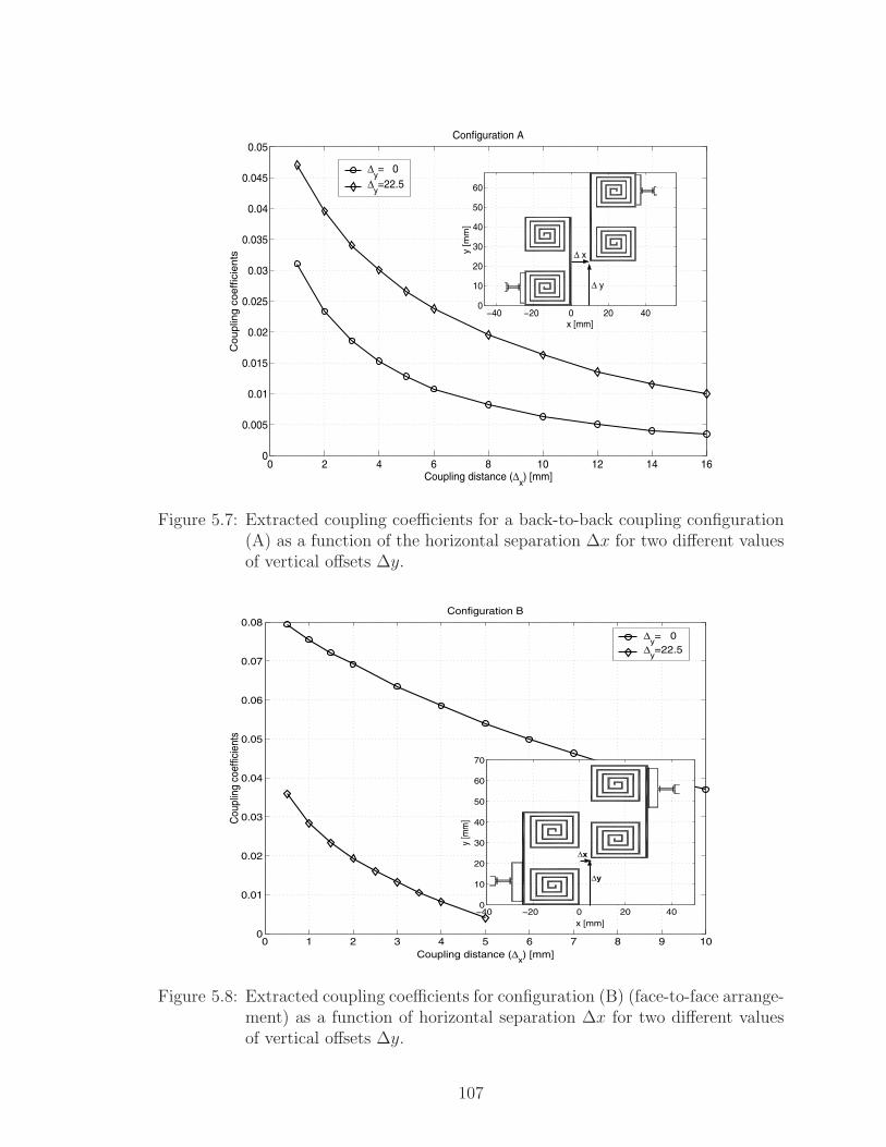
0 2 4 6 8 10 12 14 160
0.005
0.01
0.015
0.02
0.025
0.03
0.035
0.04
0.045
0.05
Coupling distance (∆x) [mm]
Co
up
ling
co
eff
icie
nts
Configuration A
−40 −20 0 20 400
10
20
30
40
50
60
x [mm]
y [m
m]
∆y= 0
∆y=22.5
∆ y
∆ x
Figure 5.7: Extracted coupling coefficients for a back-to-back coupling configuration(A) as a function of the horizontal separation ∆x for two different valuesof vertical offsets ∆y.
0 1 2 3 4 5 6 7 8 9 100
0.01
0.02
0.03
0.04
0.05
0.06
0.07
0.08
Coupling distance (∆x) [mm]
Cou
plin
g co
effic
ient
s
Configuration B
−40 −20 0 20 400
10
20
30
40
50
60
70
x [mm]
y [m
m]
∆y= 0
∆y=22.5
∆y
∆x
Figure 5.8: Extracted coupling coefficients for configuration (B) (face-to-face arrange-ment) as a function of horizontal separation ∆x for two different valuesof vertical offsets ∆y.
107
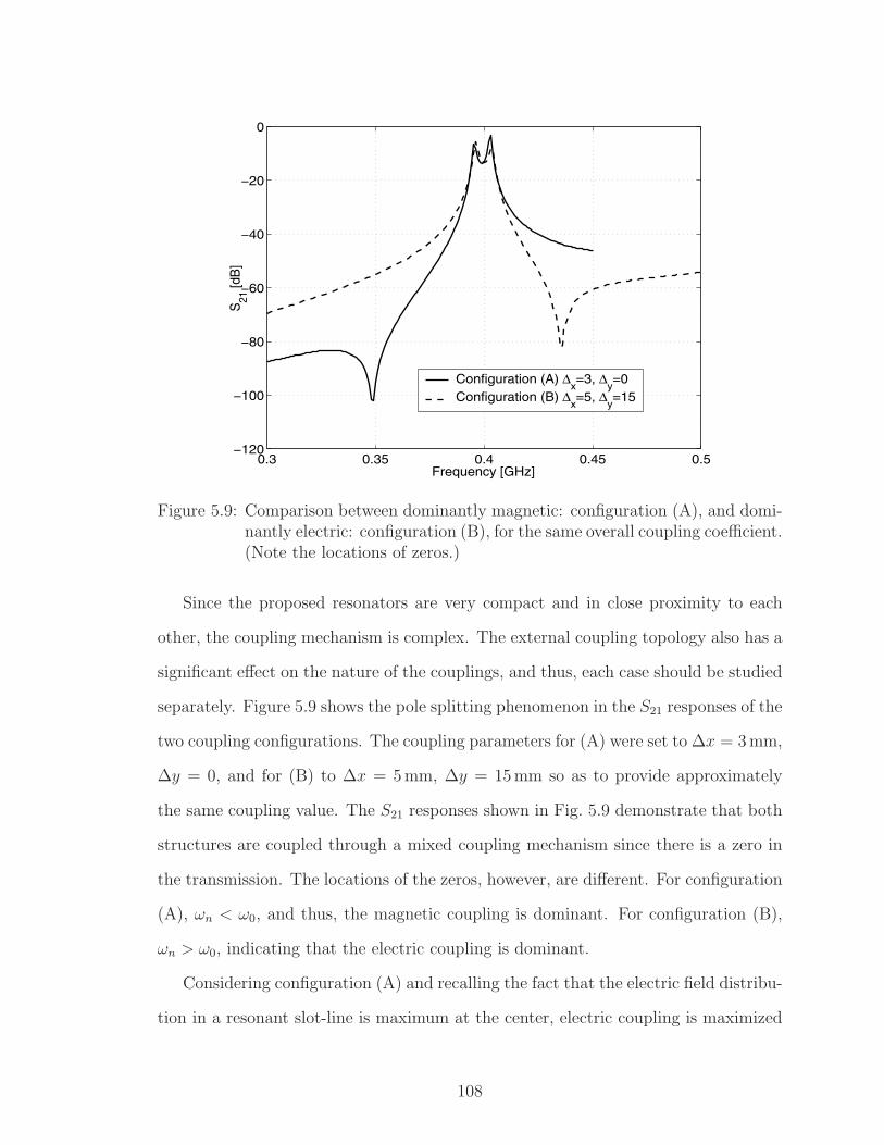
0.3 0.35 0.4 0.45 0.5−120
−100
−80
−60
−40
−20
0
Frequency [GHz]
S21
[dB
]
Configuration (A) ∆x=3, ∆
y=0
Configuration (B) ∆x=5, ∆
y=15
Figure 5.9: Comparison between dominantly magnetic: configuration (A), and domi-nantly electric: configuration (B), for the same overall coupling coefficient.(Note the locations of zeros.)
Since the proposed resonators are very compact and in close proximity to each
other, the coupling mechanism is complex. The external coupling topology also has a
significant effect on the nature of the couplings, and thus, each case should be studied
separately. Figure 5.9 shows the pole splitting phenomenon in the S21 responses of the
two coupling configurations. The coupling parameters for (A) were set to ∆x = 3 mm,
∆y = 0, and for (B) to ∆x = 5 mm, ∆y = 15 mm so as to provide approximately
the same coupling value. The S21 responses shown in Fig. 5.9 demonstrate that both
structures are coupled through a mixed coupling mechanism since there is a zero in
the transmission. The locations of the zeros, however, are different. For configuration
(A), ωn < ω0, and thus, the magnetic coupling is dominant. For configuration (B),
ωn > ω0, indicating that the electric coupling is dominant.
Considering configuration (A) and recalling the fact that the electric field distribu-
tion in a resonant slot-line is maximum at the center, electric coupling is maximized
108

when there is no vertical offset between the two resonators, namely ∆y = 0. How-
ever, it is interesting to note that although the electric coupling decreases as ∆y
increases, the overall coupling increases (See Fig. 5.7.) This behavior indicates that
magnetic coupling is dominant and electric coupling counteracts the effect of magnetic
coupling in this configuration. This behavior is also consistent with the increasing
trend of magnetic coupling as ∆y is increased, noting that the electric current linkage
(magnetic coupling) from the first resonator to the second one is increased by a factor
proportional to ∆y.
As for configuration (B), shown in Fig. 5.8, two mechanisms give rise to electric
coupling. One is the direct capacitance between the input and output, and the other
is obtained from the electric coupling between the adjacent coiled slot arms. Both
of these electric coupling components are inversely proportional to distance (∆x).
Similarly, when ∆y increases, these coupling components are reduced. Conversely, the
electric current linkage (magnetic coupling) between the two resonators is increased.
This argument confirms the fact that both types of couplings are present, and since
the overall coupling decreases with an increase in ∆y, the magnetic coupling is the
one subtracted from the dominant electric coupling.
5.3.2 External Coupling
For the miniaturized slot-line resonator, both electric and magnetic external cou-
plings can be realized. Figures 5.10 (a) and (b) illustrate input and output electric
and magnetic couplings, respectively.
Electric coupling can be controlled by the value of the interdigital capacitor in-
serted between an input or output CPW line and the slot resonator. By changing
the gap size and/or finger length of the interdigital capacitor shown in Fig. 5.10(a),
a wide range of electric external coupling values can be realized. However, note that
when the finger length of the capacitor is increased, the resonant slot length is in-
109
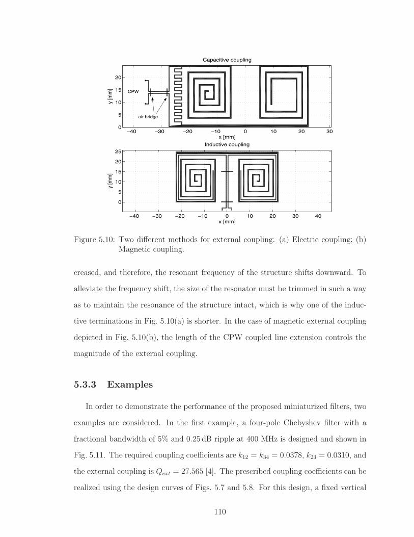
−40 −30 −20 −10 0 10 20 300
5
10
15
20
x [mm]
y [m
m]
Capacitive coupling
−40 −30 −20 −10 0 10 20 30 40
0
5
10
15
20
25
x [mm]
y [m
m]
Inductive coupling
CPW
air bridge
Figure 5.10: Two different methods for external coupling: (a) Electric coupling; (b)Magnetic coupling.
creased, and therefore, the resonant frequency of the structure shifts downward. To
alleviate the frequency shift, the size of the resonator must be trimmed in such a way
as to maintain the resonance of the structure intact, which is why one of the induc-
tive terminations in Fig. 5.10(a) is shorter. In the case of magnetic external coupling
depicted in Fig. 5.10(b), the length of the CPW coupled line extension controls the
magnitude of the external coupling.
5.3.3 Examples
In order to demonstrate the performance of the proposed miniaturized filters, two
examples are considered. In the first example, a four-pole Chebyshev filter with a
fractional bandwidth of 5% and 0.25 dB ripple at 400 MHz is designed and shown in
Fig. 5.11. The required coupling coefficients are k12 = k34 = 0.0378, k23 = 0.0310, and
the external coupling is Qext = 27.565 [4]. The prescribed coupling coefficients can be
realized using the design curves of Figs. 5.7 and 5.8. For this design, a fixed vertical
110
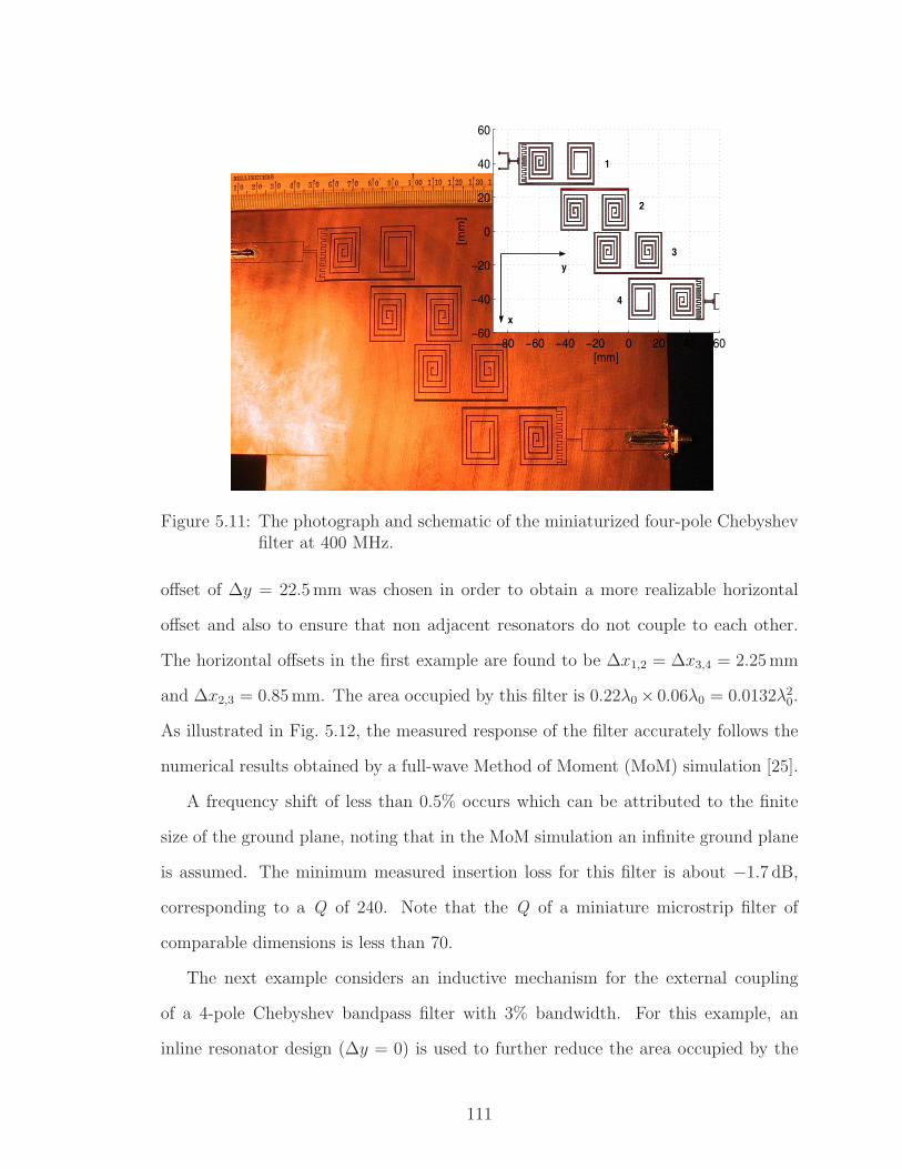
−80 −60 −40 −20 0 20 40 60−60
−40
−20
0
20
40
60
[mm]
[mm
]
x
y
1
2
3
4
Figure 5.11: The photograph and schematic of the miniaturized four-pole Chebyshevfilter at 400 MHz.
offset of ∆y = 22.5 mm was chosen in order to obtain a more realizable horizontal
offset and also to ensure that non adjacent resonators do not couple to each other.
The horizontal offsets in the first example are found to be ∆x1,2 = ∆x3,4 = 2.25 mm
and ∆x2,3 = 0.85 mm. The area occupied by this filter is 0.22λ0 × 0.06λ0 = 0.0132λ20.
As illustrated in Fig. 5.12, the measured response of the filter accurately follows the
numerical results obtained by a full-wave Method of Moment (MoM) simulation [25].
A frequency shift of less than 0.5% occurs which can be attributed to the finite
size of the ground plane, noting that in the MoM simulation an infinite ground plane
is assumed. The minimum measured insertion loss for this filter is about −1.7 dB,
corresponding to a Q of 240. Note that the Q of a miniature microstrip filter of
comparable dimensions is less than 70.
The next example considers an inductive mechanism for the external coupling
of a 4-pole Chebyshev bandpass filter with 3% bandwidth. For this example, an
inline resonator design (∆y = 0) is used to further reduce the area occupied by the
111
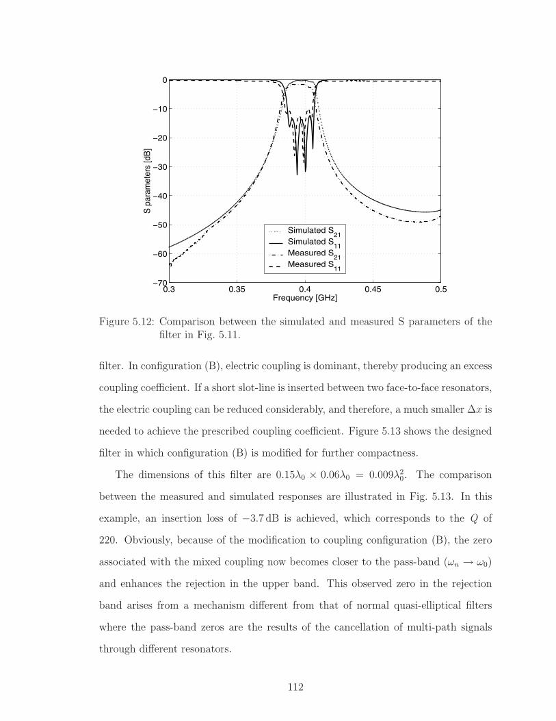
0.3 0.35 0.4 0.45 0.5−70
−60
−50
−40
−30
−20
−10
0
Frequency [GHz]
S p
aram
eter
s [d
B]
Simulated S21
Simulated S11
Measured S21
Measured S11
Figure 5.12: Comparison between the simulated and measured S parameters of thefilter in Fig. 5.11.
filter. In configuration (B), electric coupling is dominant, thereby producing an excess
coupling coefficient. If a short slot-line is inserted between two face-to-face resonators,
the electric coupling can be reduced considerably, and therefore, a much smaller ∆x is
needed to achieve the prescribed coupling coefficient. Figure 5.13 shows the designed
filter in which configuration (B) is modified for further compactness.
The dimensions of this filter are 0.15λ0 × 0.06λ0 = 0.009λ20. The comparison
between the measured and simulated responses are illustrated in Fig. 5.13. In this
example, an insertion loss of −3.7 dB is achieved, which corresponds to the Q of
220. Obviously, because of the modification to coupling configuration (B), the zero
associated with the mixed coupling now becomes closer to the pass-band (ωn → ω0)
and enhances the rejection in the upper band. This observed zero in the rejection
band arises from a mechanism different from that of normal quasi-elliptical filters
where the pass-band zeros are the results of the cancellation of multi-path signals
through different resonators.
112
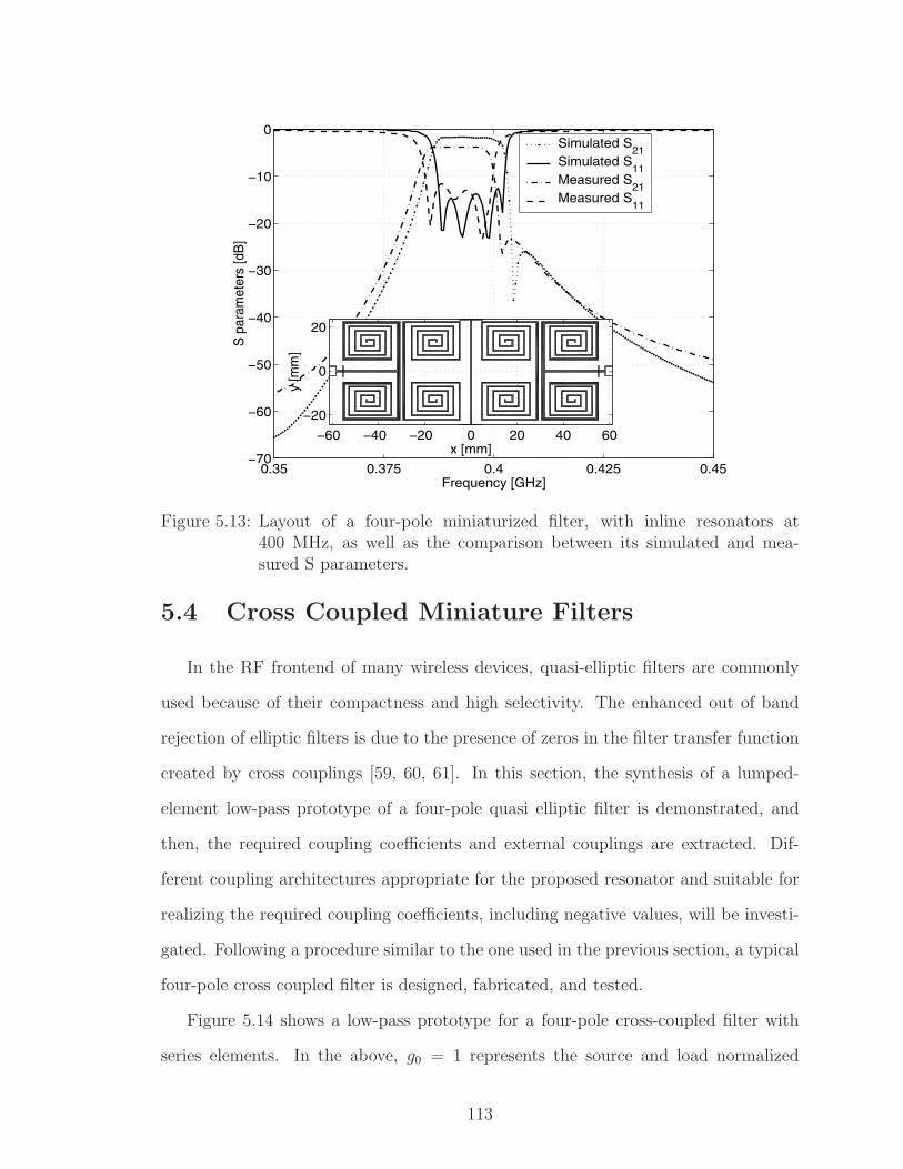
0.35 0.375 0.4 0.425 0.45−70
−60
−50
−40
−30
−20
−10
0
Frequency [GHz]
S p
aram
eter
s [d
B]
Simulated S21
Simulated S11
Measured S21
Measured S11
−60 −40 −20 0 20 40 60
−20
0
20
x [mm]
y [m
m]
Figure 5.13: Layout of a four-pole miniaturized filter, with inline resonators at400 MHz, as well as the comparison between its simulated and mea-sured S parameters.
5.4 Cross Coupled Miniature Filters
In the RF frontend of many wireless devices, quasi-elliptic filters are commonly
used because of their compactness and high selectivity. The enhanced out of band
rejection of elliptic filters is due to the presence of zeros in the filter transfer function
created by cross couplings [59, 60, 61]. In this section, the synthesis of a lumped-
element low-pass prototype of a four-pole quasi elliptic filter is demonstrated, and
then, the required coupling coefficients and external couplings are extracted. Dif-
ferent coupling architectures appropriate for the proposed resonator and suitable for
realizing the required coupling coefficients, including negative values, will be investi-
gated. Following a procedure similar to the one used in the previous section, a typical
four-pole cross coupled filter is designed, fabricated, and tested.
Figure 5.14 shows a low-pass prototype for a four-pole cross-coupled filter with
series elements. In the above, g0 = 1 represents the source and load normalized
113
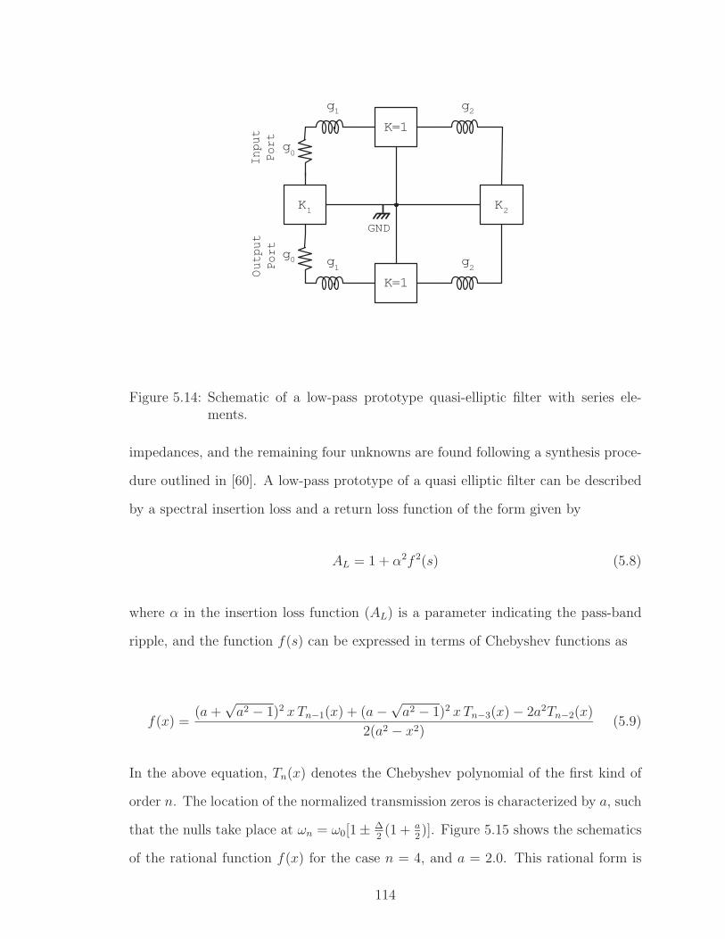
g1 g2
g1
g2
K2K1
K=1
K=1
g0
g0
GND
Input
Port
Output
Port
Figure 5.14: Schematic of a low-pass prototype quasi-elliptic filter with series ele-ments.
impedances, and the remaining four unknowns are found following a synthesis proce-
dure outlined in [60]. A low-pass prototype of a quasi elliptic filter can be described
by a spectral insertion loss and a return loss function of the form given by
AL = 1 + α2f 2(s) (5.8)
where α in the insertion loss function (AL) is a parameter indicating the pass-band
ripple, and the function f(s) can be expressed in terms of Chebyshev functions as
f(x) =(a +
√a2 − 1)2 xTn−1(x) + (a −√
a2 − 1)2 xTn−3(x) − 2a2Tn−2(x)
2(a2 − x2)(5.9)
In the above equation, Tn(x) denotes the Chebyshev polynomial of the first kind of
order n. The location of the normalized transmission zeros is characterized by a, such
that the nulls take place at ωn = ω0[1± ∆2(1 + a
2)]. Figure 5.15 shows the schematics
of the rational function f(x) for the case n = 4, and a = 2.0. This rational form is
114
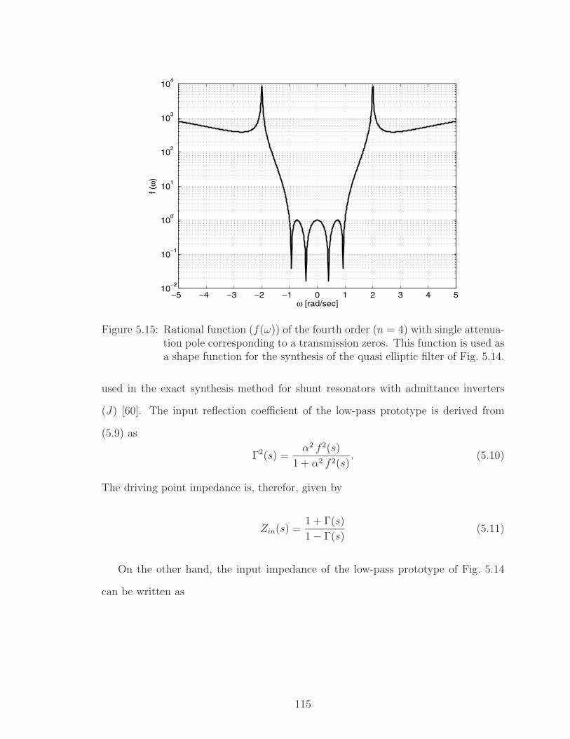
−5 −4 −3 −2 −1 0 1 2 3 4 510
−2
10−1
100
101
102
103
104
ω [rad/sec]
f (ω)
Figure 5.15: Rational function (f(ω)) of the fourth order (n = 4) with single attenua-tion pole corresponding to a transmission zeros. This function is used asa shape function for the synthesis of the quasi elliptic filter of Fig. 5.14.
used in the exact synthesis method for shunt resonators with admittance inverters
(J) [60]. The input reflection coefficient of the low-pass prototype is derived from
(5.9) as
Γ2(s) =α2 f 2(s)
1 + α2 f 2(s). (5.10)
The driving point impedance is, therefor, given by
Zin(s) =1 + Γ(s)
1 − Γ(s)(5.11)
On the other hand, the input impedance of the low-pass prototype of Fig. 5.14
can be written as
115
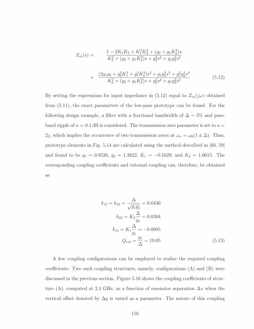
Zin(s) =1 − 2K1K2 + K2
1K22 + (g2 + g1K
22)s
K22 + (g2 + g1K2
2)s + g22s
2 + g1g22s
3
+(2g1g2 + g2
2K21 + g2
1K22)s2 + g1g
22s
3 + g21g
22s
4
K22 + (g2 + g1K2
2)s + g22s
2 + g1g22s
3(5.12)
By setting the expressions for input impedance in (5.12) equal to Zin(jω) obtained
from (5.11), the exact parameters of the low-pass prototype can be found. For the
following design example, a filter with a fractional bandwidth of ∆ = 5% and pass-
band ripple of α = 0.1 dB is considered. The transmission zero parameter is set to a =
2j, which implies the occurrence of two transmission zeros at ωn = ω0(1±∆). Thus,
prototype elements in Fig. 5.14 are calculated using the method described in [60, 59]
and found to be g1 = 0.9526, g2 = 1.3822, K1 = −0.1629, and K2 = 1.0615. The
corresponding coupling coefficients and external coupling can, therefore, be obtained
as
k12 = k34 =∆√g1g2
= 0.0436
k23 = K2∆
g2
= 0.0384
k14 = K1∆
g1
= −0.0085
Qext =g1
∆= 19.05 (5.13)
A few coupling configurations can be employed to realize the required coupling
coefficients. Two such coupling structures, namely, configurations (A) and (B) were
discussed in the previous section. Figure 5.16 shows the coupling coefficients of struc-
ture (A), computed at 2.4 GHz, as a function of resonator separation ∆x when the
vertical offset denoted by ∆y is varied as a parameter. The nature of this coupling
116
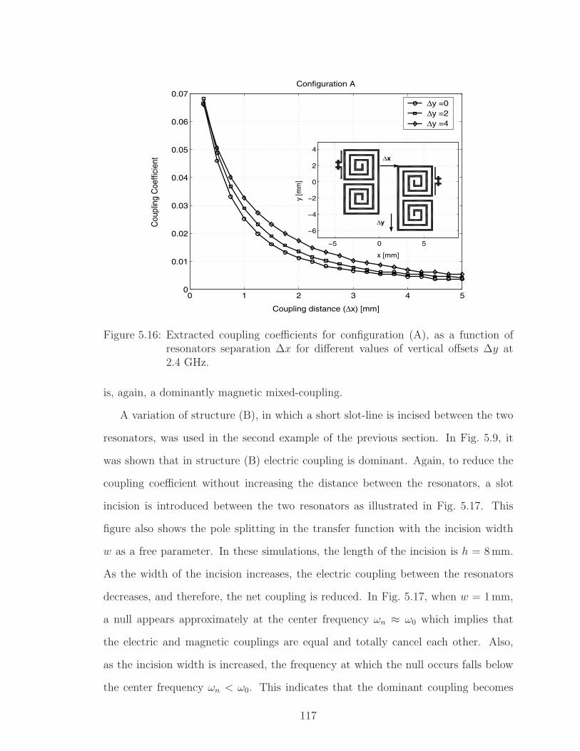
0 1 2 3 4 50
0.01
0.02
0.03
0.04
0.05
0.06
0.07
Coupling distance (∆x) [mm]
Cou
plin
g C
oeffi
cien
t
Configuration A
−5 0 5
−6
−4
−2
0
2
4
x [mm]
y [m
m]
∆y =0∆y =2∆y =4
∆x
∆y
Figure 5.16: Extracted coupling coefficients for configuration (A), as a function ofresonators separation ∆x for different values of vertical offsets ∆y at2.4 GHz.
is, again, a dominantly magnetic mixed-coupling.
A variation of structure (B), in which a short slot-line is incised between the two
resonators, was used in the second example of the previous section. In Fig. 5.9, it
was shown that in structure (B) electric coupling is dominant. Again, to reduce the
coupling coefficient without increasing the distance between the resonators, a slot
incision is introduced between the two resonators as illustrated in Fig. 5.17. This
figure also shows the pole splitting in the transfer function with the incision width
w as a free parameter. In these simulations, the length of the incision is h = 8 mm.
As the width of the incision increases, the electric coupling between the resonators
decreases, and therefore, the net coupling is reduced. In Fig. 5.17, when w = 1 mm,
a null appears approximately at the center frequency ωn ≈ ω0 which implies that
the electric and magnetic couplings are equal and totally cancel each other. Also,
as the incision width is increased, the frequency at which the null occurs falls below
the center frequency ωn < ω0. This indicates that the dominant coupling becomes
117
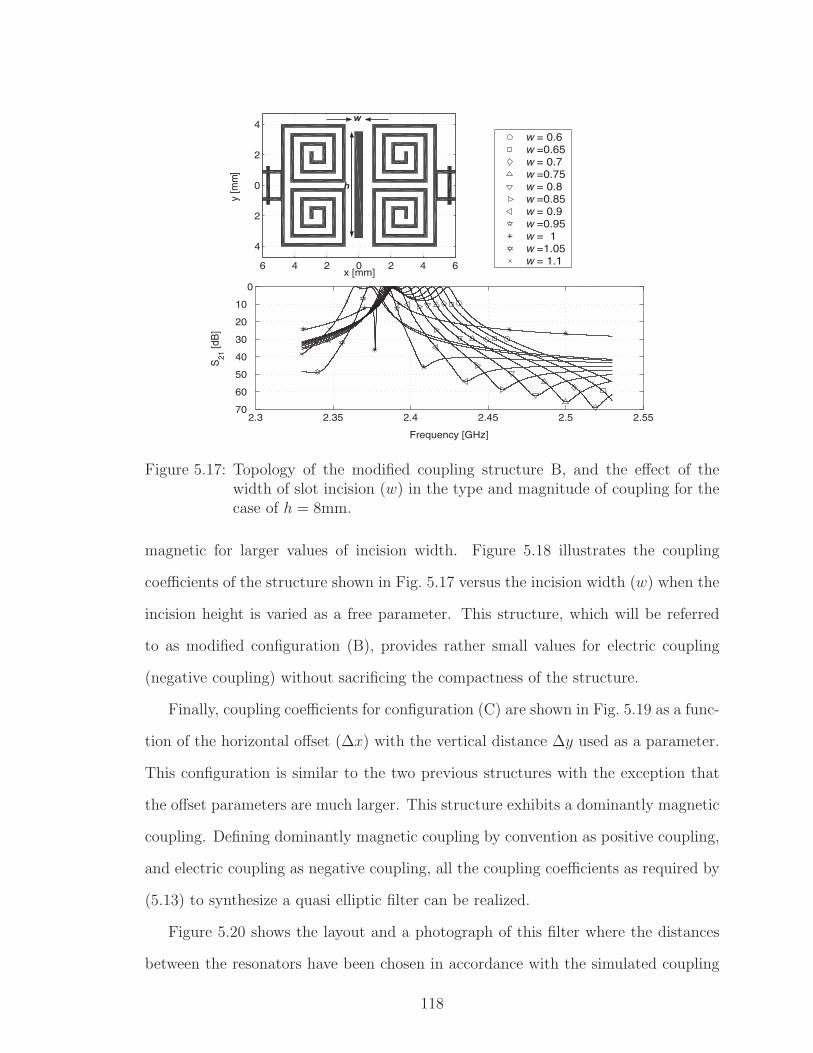
2.3 2.35 2.4 2.45 2.5 2.5570
60
50
40
30
20
10
0
Frequency [GHz]
S21
[dB
]
6 4 2 0 2 4 6
4
2
0
2
4
x [mm]
y [m
m]
w = 0.6w =0.65w = 0.7w =0.75w = 0.8w =0.85w = 0.9w =0.95w = 1w =1.05w = 1.1
w
h
Figure 5.17: Topology of the modified coupling structure B, and the effect of thewidth of slot incision (w) in the type and magnitude of coupling for thecase of h = 8mm.
magnetic for larger values of incision width. Figure 5.18 illustrates the coupling
coefficients of the structure shown in Fig. 5.17 versus the incision width (w) when the
incision height is varied as a free parameter. This structure, which will be referred
to as modified configuration (B), provides rather small values for electric coupling
(negative coupling) without sacrificing the compactness of the structure.
Finally, coupling coefficients for configuration (C) are shown in Fig. 5.19 as a func-
tion of the horizontal offset (∆x) with the vertical distance ∆y used as a parameter.
This configuration is similar to the two previous structures with the exception that
the offset parameters are much larger. This structure exhibits a dominantly magnetic
coupling. Defining dominantly magnetic coupling by convention as positive coupling,
and electric coupling as negative coupling, all the coupling coefficients as required by
(5.13) to synthesize a quasi elliptic filter can be realized.
Figure 5.20 shows the layout and a photograph of this filter where the distances
between the resonators have been chosen in accordance with the simulated coupling
118
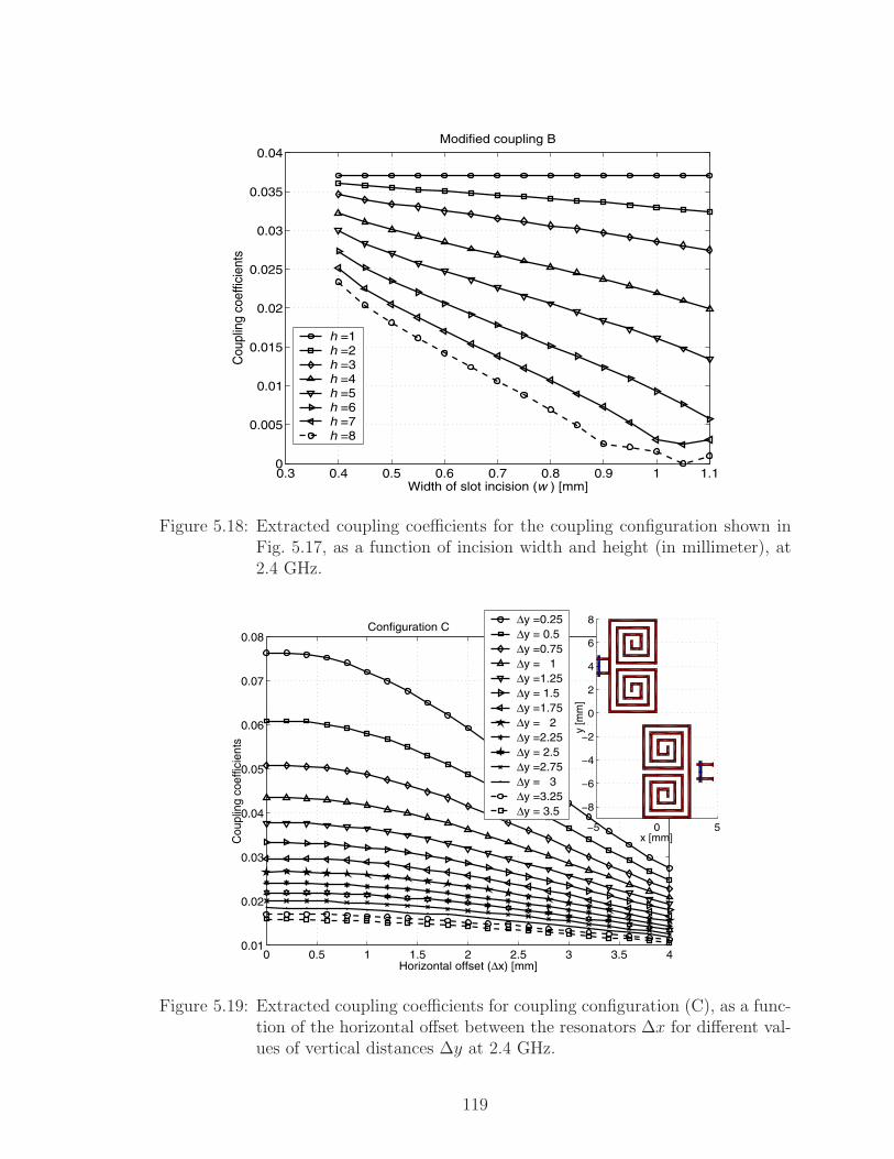
0.3 0.4 0.5 0.6 0.7 0.8 0.9 1 1.10
0.005
0.01
0.015
0.02
0.025
0.03
0.035
0.04
Width of slot incision (w ) [mm]
Cou
plin
g co
effic
ient
s
Modified coupling B
h =1h =2h =3h =4h =5h =6h =7h =8
Figure 5.18: Extracted coupling coefficients for the coupling configuration shown inFig. 5.17, as a function of incision width and height (in millimeter), at2.4 GHz.
0 0.5 1 1.5 2 2.5 3 3.5 40.01
0.02
0.03
0.04
0.05
0.06
0.07
0.08
Horizontal offset (∆x) [mm]
Cou
plin
g co
effic
ient
s
Configuration C
−5 0 5
−8
−6
−4
−2
0
2
4
6
8
y [m
m]
x [mm]
∆y =0.25∆y = 0.5∆y =0.75∆y = 1∆y =1.25∆y = 1.5∆y =1.75∆y = 2∆y =2.25∆y = 2.5∆y =2.75∆y = 3∆y =3.25∆y = 3.5
Figure 5.19: Extracted coupling coefficients for coupling configuration (C), as a func-tion of the horizontal offset between the resonators ∆x for different val-ues of vertical distances ∆y at 2.4 GHz.
119
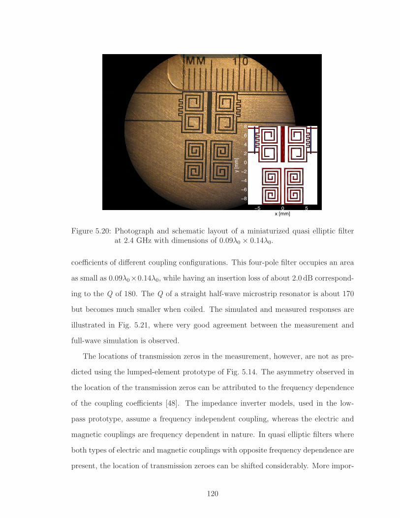
−5 0 5
−8
−6
−4
−2
0
2
4
6
8
x [mm]
y [m
m]
Figure 5.20: Photograph and schematic layout of a miniaturized quasi elliptic filterat 2.4 GHz with dimensions of 0.09λ0 × 0.14λ0.
coefficients of different coupling configurations. This four-pole filter occupies an area
as small as 0.09λ0×0.14λ0, while having an insertion loss of about 2.0 dB correspond-
ing to the Q of 180. The Q of a straight half-wave microstrip resonator is about 170
but becomes much smaller when coiled. The simulated and measured responses are
illustrated in Fig. 5.21, where very good agreement between the measurement and
full-wave simulation is observed.
The locations of transmission zeros in the measurement, however, are not as pre-
dicted using the lumped-element prototype of Fig. 5.14. The asymmetry observed in
the location of the transmission zeros can be attributed to the frequency dependence
of the coupling coefficients [48]. The impedance inverter models, used in the low-
pass prototype, assume a frequency independent coupling, whereas the electric and
magnetic couplings are frequency dependent in nature. In quasi elliptic filters where
both types of electric and magnetic couplings with opposite frequency dependence are
present, the location of transmission zeroes can be shifted considerably. More impor-
120
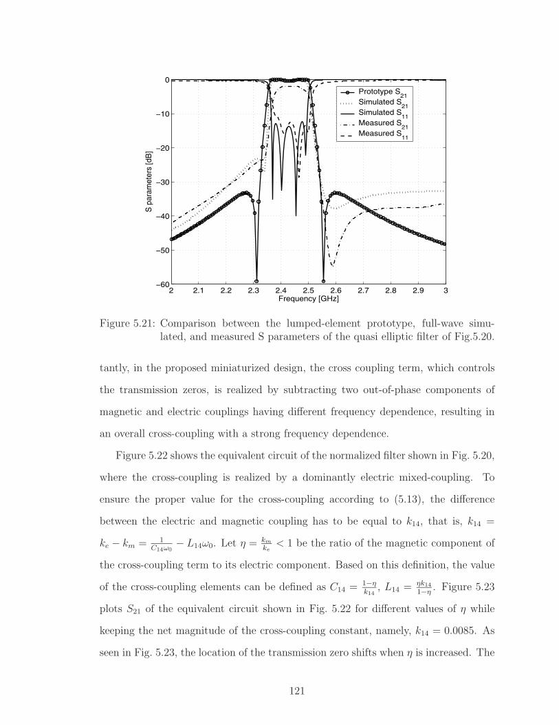
2 2.1 2.2 2.3 2.4 2.5 2.6 2.7 2.8 2.9 3−60
−50
−40
−30
−20
−10
0
Frequency [GHz]
S p
aram
eter
s [d
B]
Prototype S21
Simulated S21
Simulated S11
Measured S21
Measured S11
Figure 5.21: Comparison between the lumped-element prototype, full-wave simu-lated, and measured S parameters of the quasi elliptic filter of Fig.5.20.
tantly, in the proposed miniaturized design, the cross coupling term, which controls
the transmission zeros, is realized by subtracting two out-of-phase components of
magnetic and electric couplings having different frequency dependence, resulting in
an overall cross-coupling with a strong frequency dependence.
Figure 5.22 shows the equivalent circuit of the normalized filter shown in Fig. 5.20,
where the cross-coupling is realized by a dominantly electric mixed-coupling. To
ensure the proper value for the cross-coupling according to (5.13), the difference
between the electric and magnetic coupling has to be equal to k14, that is, k14 =
ke − km = 1C14ω0
− L14ω0. Let η = km
ke< 1 be the ratio of the magnetic component of
the cross-coupling term to its electric component. Based on this definition, the value
of the cross-coupling elements can be defined as C14 = 1−ηk14
, L14 = ηk14
1−η. Figure 5.23
plots S21 of the equivalent circuit shown in Fig. 5.22 for different values of η while
keeping the net magnitude of the cross-coupling constant, namely, k14 = 0.0085. As
seen in Fig. 5.23, the location of the transmission zero shifts when η is increased. The
121
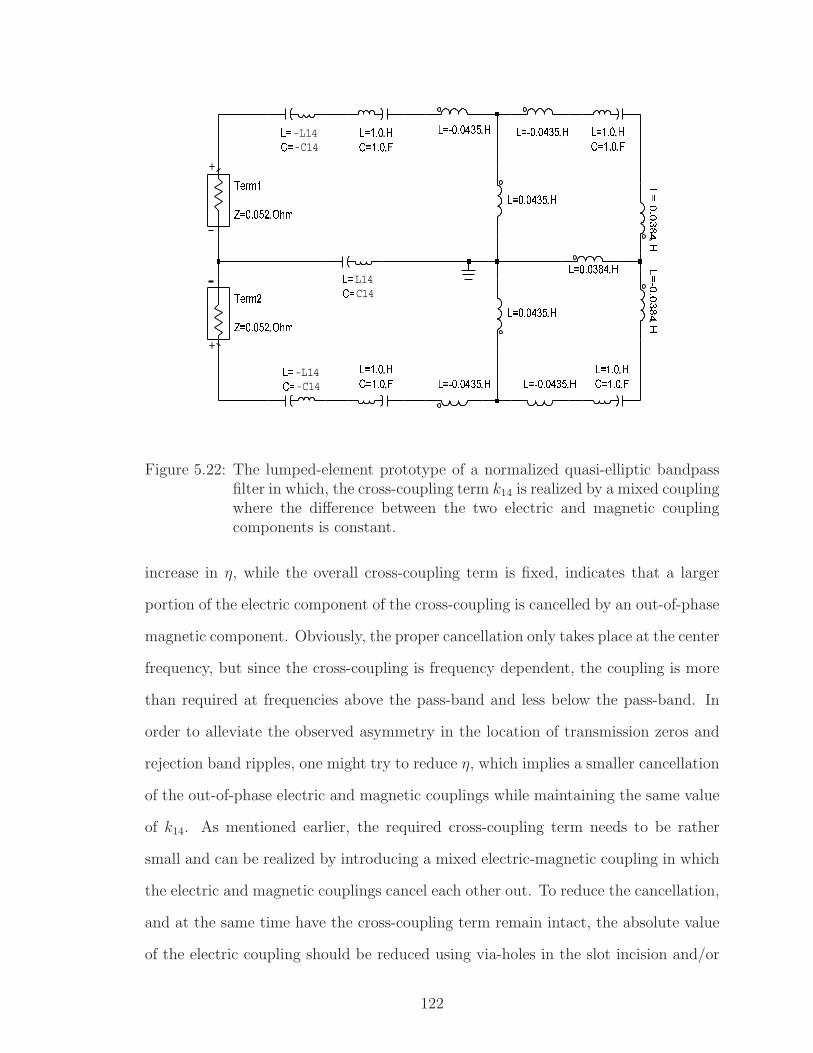
+
+
-L14-C14
L14C14
-L14-C14
Figure 5.22: The lumped-element prototype of a normalized quasi-elliptic bandpassfilter in which, the cross-coupling term k14 is realized by a mixed couplingwhere the difference between the two electric and magnetic couplingcomponents is constant.
increase in η, while the overall cross-coupling term is fixed, indicates that a larger
portion of the electric component of the cross-coupling is cancelled by an out-of-phase
magnetic component. Obviously, the proper cancellation only takes place at the center
frequency, but since the cross-coupling is frequency dependent, the coupling is more
than required at frequencies above the pass-band and less below the pass-band. In
order to alleviate the observed asymmetry in the location of transmission zeros and
rejection band ripples, one might try to reduce η, which implies a smaller cancellation
of the out-of-phase electric and magnetic couplings while maintaining the same value
of k14. As mentioned earlier, the required cross-coupling term needs to be rather
small and can be realized by introducing a mixed electric-magnetic coupling in which
the electric and magnetic couplings cancel each other out. To reduce the cancellation,
and at the same time have the cross-coupling term remain intact, the absolute value
of the electric coupling should be reduced using via-holes in the slot incision and/or
122
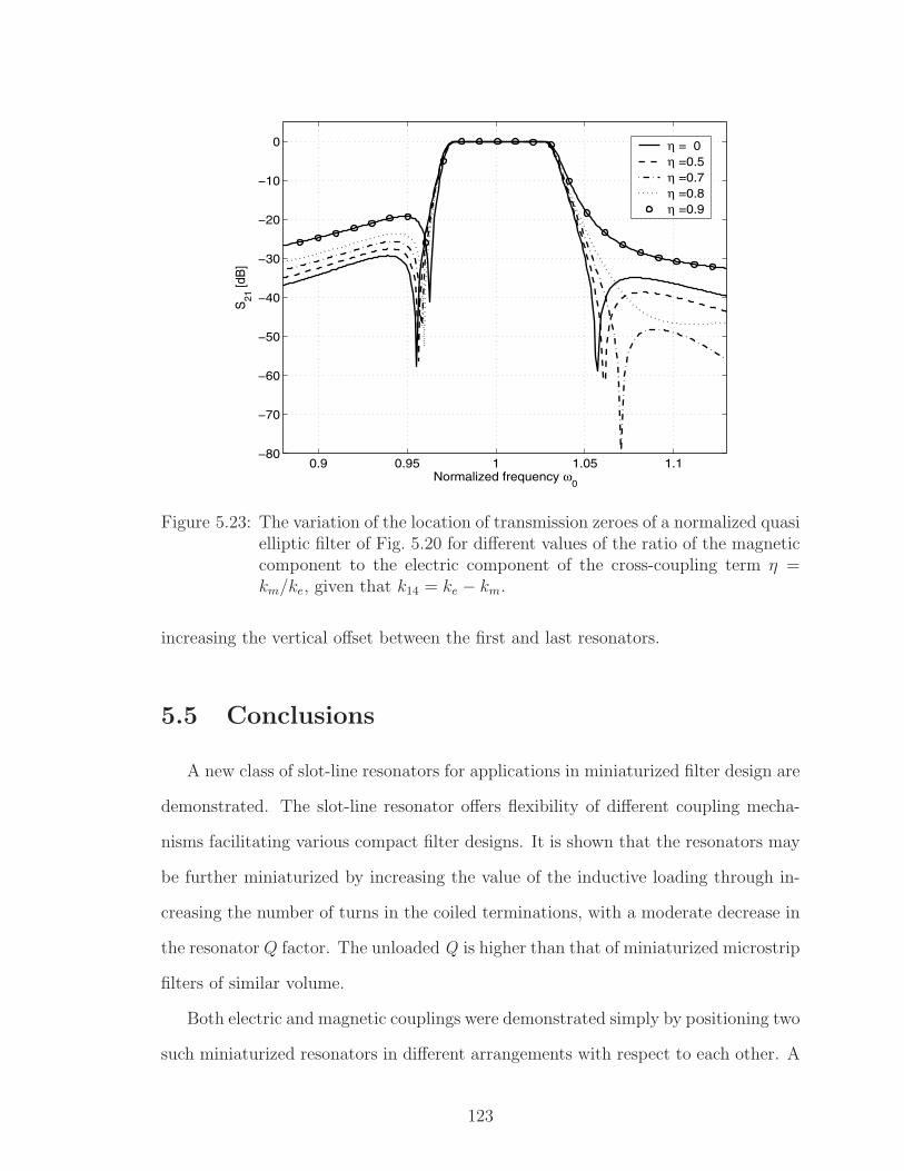
0.9 0.95 1 1.05 1.1−80
−70
−60
−50
−40
−30
−20
−10
0
Normalized frequency ω0
S21
[dB
]
η = 0η =0.5η =0.7η =0.8η =0.9
Figure 5.23: The variation of the location of transmission zeroes of a normalized quasielliptic filter of Fig. 5.20 for different values of the ratio of the magneticcomponent to the electric component of the cross-coupling term η =km/ke, given that k14 = ke − km.
increasing the vertical offset between the first and last resonators.
5.5 Conclusions
A new class of slot-line resonators for applications in miniaturized filter design are
demonstrated. The slot-line resonator offers flexibility of different coupling mecha-
nisms facilitating various compact filter designs. It is shown that the resonators may
be further miniaturized by increasing the value of the inductive loading through in-
creasing the number of turns in the coiled terminations, with a moderate decrease in
the resonator Q factor. The unloaded Q is higher than that of miniaturized microstrip
filters of similar volume.
Both electric and magnetic couplings were demonstrated simply by positioning two
such miniaturized resonators in different arrangements with respect to each other. A
123
straightforward method was given to determine whether the coupling mechanism is
magnetic or electric. A full-wave analysis was used to extract the coupling coefficients
used in the filter design.
To demonstrate the validity of the approach, three examples were studied includ-
ing two four-pole Chebyshev filters, one of which used a mixed coupling structure, and
a four-pole quasi elliptic filter. The agreement between the simulated and measured
responses of these filters was shown to be excellent.
The prototype Chebyshev filters at 400 MHz with fractional bandwidths of 5%
and 3% show insertion loss values of about 1.7 dB, and 3.7 dB, while occupying a
very small rectangular area of 0.22λ0×0.06λ0, and 0.15λ0×0.06λ0, respectively. The
unloaded Q of these filters is about three times greater than those of their microstrip
counterparts.
A four-pole quasi-elliptic filter with ∆ = 5% at 2.4 GHz was also fabricated, and
its measured response was compared with numerical simulation. This filter with an
improved out of band rejection gives 2 dB insertion loss while occupying a very small
area of about 0.09λ0 × 0.14λ0. The effect of the frequency dependent cross-coupling
on the quasi-elliptic filter was also investigated and shown to delineate the asymmetry
in the rejection band and transmission zeroes.
124
CHAPTER 6
RCS Measurement Technique to Extract the Input
Impedance of High-Impedance Miniaturized Slot
Antennas
6.1 Introduction
In the wake of recent interests in micro- and nano-technologies, there is an ongoing
effort towards the application of these emerging technologies in the fabrication of
different devices, components, and circuits. One severe concern in dealing with such
devices is their high impedance –due to their extremely small size– rendering them
very difficult to test and characterize. The difference between the impedance level of
nano-devices and that of standard RF and microwave components is so immense that
makes any kind of matching network prohibitively lossy, and thus, impractical.
MEMS resonators/filters are an example of very high-impedance microsystems
(10 K Ω− 20 K Ω). Therefore, they require high-impedance antennas and RF circuits
to be integrated with in order for them to be utilized for wireless and sensor network
applications.
The interest in high-impedance components is not restricted to micro and nano
applications. High-impedance components may find some applications in other areas,
125

such as electronics. Although electronic devices are traditionally sought for operation
with 50 Ω systems, they can be made high-impedance to reduce the transceiver power.
For example, in the MOSFET design, the size of the gate is increased to accommodate
for matchable impedances to a 50 Ω line. By reducing the gate size, the impedance
increases, which in turn reduces the power consumption drastically. Given that a
high-impedance antenna is available, the impedance of the electronic devices can
be reduced to obtain a minimum power, without any need for additional matching
networks.
In response to aforementioned needs, significant effort has been devoted to de-
sign a high-impedance miniature antenna by modifying the miniaturized slot antenna
presented in Chapter 3. Remembering from Chapters 3, and 4, miniaturization re-
duces the physical aperture and the radiation conductance of the antenna. This
effect can be exploited to yield a high-impedance antenna. One of the main chal-
lenges of high-impedance antennas, as well as any other high-impedance RF circuit,
is the measurement of very high impedances. High-impedance measurement becomes
intractable at higher frequencies using currently available microwave measurement
instruments since they are designed for standard 50 Ω line. The standard impedance
is adopted because it is an optimal point where a low conduction loss with reasonable
transmission line dimensions can be achieved. In practice, the impedance of a mi-
crowave transmission line cannot go beyond 80 Ω − 90 Ω; even so, they become very
lossy and start to radiate as the frequency increases.
The main objective of this chapter is to demonstrate that the miniaturized slot
antennas, which were presented in this thesis, can exhibit a very high radiation resis-
tance on the order of a few kilo-ohms. At lower region of microwave frequency up to
about 3 GHz, high impedances can be measured using the RF Impedance/Material
Analyzer.1 The impedance analyzer is used to measure the input impedance of a
1Agilent E4991A RF Impedance/Material Analyzer.
126

prototype miniature slot antenna at UHF. This instrument, however, cannot be used
for frequencies higher than 3 GHz, and thus, an alternative technique is required.
For higher frequencies, a novel technique to measure the input impedance of gen-
erally high-impedance miniaturized slot/aperture antennas are introduced whereby a
relationship is established between the RCS of a slot/apreture antenna to its termi-
nating impedance/conductance. Then, the necessary condition of the RCS that must
be satisfied when the receiving antenna is terminated by a matched load is derived
and used to identify the corresponding RCS. Examining the RCS of the loaded an-
tenna against the criteria provided by the proposed method can determine whether
the receiving antenna is matched or not. If not, one can change the termination resis-
tance till the required conditions on the RCS are met, and then, identify the matched
load, which is equal to the impedance of the antenna at resonance.
6.2 Methodology
In order to establish a relationship between the RCS of a slot/aperture antenna
and its load impedance, first a resonant half-wave slot antenna is considered. Al-
though the center-fed slot antenna is not so high-impedance as of MEMS or nano-
devices, its impedance is on around 500 Ω, which is still an order of magnitude larger
than that of a standard transmission line. Furthermore, its radiated and scattered
fields can be analytically calculated using Babinet’s principle and Bookers’ relation
[62, 37].
Consider an infinite perfectly electric conducting (PEC) screen with a narrow half-
wavelength aperture, and its complimentary structure consisting of a thin strip of PEC
as displayed in Fig. 6.1(a) and (b), respectively. Figure 6.1(c) shows a thin perfectly
magnetic conducting (PMC) strip of the same size as the PEC strip of Fig. 6.1(b).
The objective of the proposed measurement technique is to infer the impedance of the
127
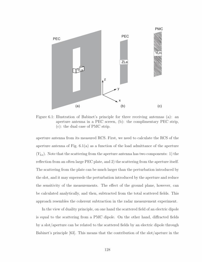
YLa
(a) (b) (c)
PECPEC
PMC
ZLe
YLm
y
x
z
Figure 6.1: Illustration of Babinet’s principle for three receiving antennas (a): anaperture antenna in a PEC screen, (b): the complimentary PEC strip,(c): the dual case of PMC strip.
aperture antenna from its measured RCS. First, we need to calculate the RCS of the
aperture antenna of Fig. 6.1(a) as a function of the load admittance of the aperture
(YLa). Note that the scattering from the aperture antenna has two components: 1) the
reflection from an often large PEC plate, and 2) the scattering from the aperture itself.
The scattering from the plate can be much larger than the perturbation introduced by
the slot, and it may supersede the perturbation introduced by the aperture and reduce
the sensitivity of the measurements. The effect of the ground plane, however, can
be calculated analytically, and then, subtracted from the total scattered fields. This
approach resembles the coherent subtraction in the radar measurement experiment.
In the view of duality principle, on one hand the scattered field of an electric dipole
is equal to the scattering from a PMC dipole. On the other hand, diffracted fields
by a slot/aperture can be related to the scattered fields by an electric dipole through
Babinet’s principle [63]. This means that the contribution of the slot/apeture in the
128

total scattered field from a slot antenna can be calculated analytically.
6.3 Formulation
In this section, we seek an analytical formulation of electromagnetic scattering
from three different receiving antenna structures depicted in Fig. 6.1.
6.3.1 Scattering from an Electric-Dipole Antenna
Figure 6.1(b) shows the electric dipole antenna illuminated by a plane wave prop-
agating along the −x direction of the form:
E i = zE0ejkx (6.1)
Using the reciprocity theorem, the scattered fields of the received antenna is reciprocal
to the radiated fields of the same antenna in the transmit mode. Therefore, the
formulation for the radiation pattern of a half-wavelength dipole antenna can be used
to obtain the scattered field of a resonant electric dipole [34]; that is,
Eθ jηIine
−jkr
2πr
cos(π2
cos θ)
sin θ(6.2)
An antenna in the receive mode is used to intercept electromagnetic waves and to
extract power form them. For any antenna, the effective length can be defined [34].
The effective length is a vector quantity to determine the induced open-circuit voltage
of the antenna when antenna is illuminated by electromagnetic waves. This param-
eter is basically defined in accordance with Faraday’s Law, wherein the open-circuit
voltage is defined as voc =∮
E.d. Note that the effective length is related to the
far-field of the antenna, and given by [34, 64]
129

Ea = aθEθ + aφEφ = −jηkIin
4πreff e−jkr (6.3)
Based on the definition of the effective length, the open-circuit voltage of an antenna
in the receive mode is related to the incident wave and the effective length of the
antenna using
Voc = Ei · eff . (6.4)
In a case where the incident wave is assumed to impinge on the antenna from the
direction of the maximum gain, namely, θ = 90, invoking (6.4) gives the open-circuit
voltage of the resonant electric dipole as
Voc = 2E0
k(6.5)
Thus, the current at the input terminal of the antenna as a function of the load is
found to be
Iin(ZL) =2E0/k
Zant + ZL
(6.6)
In the above, Zant and ZL stand for the input impedance of the antenna and the load
impedance, respectively. Substituting the input current from (6.6) in (6.2) gives an
expression for the scattered field of a resonant electric dipole at the broad side as
Es
e = jη2E0/k
Ze + ZLe
e−jkr
2πr(6.7)
The radar cross-section of the electric dipole in the peak direction (θ = 90) is,
therefore, calculated to be
σe = 4πR2 |Es
Ei|2 =
4η2
πk2|Ze + ZLe|2 (6.8)
130
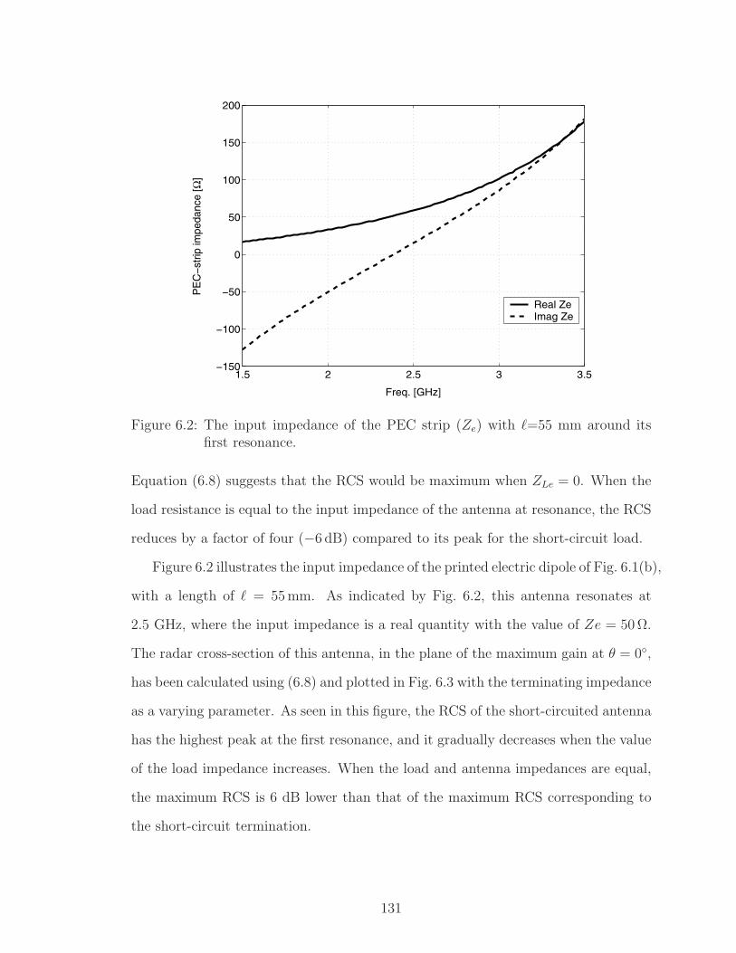
1.5 2 2.5 3 3.5−150
−100
−50
0
50
100
150
200
Freq. [GHz]
PE
C−s
trip
impe
danc
e [Ω
]
Real ZeImag Ze
Figure 6.2: The input impedance of the PEC strip (Ze) with =55 mm around itsfirst resonance.
Equation (6.8) suggests that the RCS would be maximum when ZLe = 0. When the
load resistance is equal to the input impedance of the antenna at resonance, the RCS
reduces by a factor of four (−6 dB) compared to its peak for the short-circuit load.
Figure 6.2 illustrates the input impedance of the printed electric dipole of Fig. 6.1(b),
with a length of = 55 mm. As indicated by Fig. 6.2, this antenna resonates at
2.5 GHz, where the input impedance is a real quantity with the value of Ze = 50 Ω.
The radar cross-section of this antenna, in the plane of the maximum gain at θ = 0,
has been calculated using (6.8) and plotted in Fig. 6.3 with the terminating impedance
as a varying parameter. As seen in this figure, the RCS of the short-circuited antenna
has the highest peak at the first resonance, and it gradually decreases when the value
of the load impedance increases. When the load and antenna impedances are equal,
the maximum RCS is 6 dB lower than that of the maximum RCS corresponding to
the short-circuit termination.
131
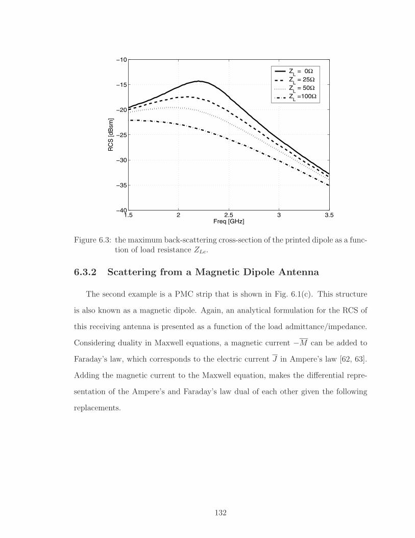
1.5 2 2.5 3 3.5−40
−35
−30
−25
−20
−15
−10
Freq [GHz]
RC
S [d
Bsm
]
ZL = 0Ω
ZL = 25Ω
ZL = 50Ω
ZL =100Ω
Figure 6.3: the maximum back-scattering cross-section of the printed dipole as a func-tion of load resistance ZLe.
6.3.2 Scattering from a Magnetic Dipole Antenna
The second example is a PMC strip that is shown in Fig. 6.1(c). This structure
is also known as a magnetic dipole. Again, an analytical formulation for the RCS of
this receiving antenna is presented as a function of the load admittance/impedance.
Considering duality in Maxwell equations, a magnetic current −M can be added to
Faraday’s law, which corresponds to the electric current J in Ampere’s law [62, 63].
Adding the magnetic current to the Maxwell equation, makes the differential repre-
sentation of the Ampere’s and Faraday’s law dual of each other given the following
replacements.
132
E → H
H → −E
J → M
M → −J
µ → ε
ε → µ
η → 1
η(6.9)
The PMC strip of Fig. 6.1(c) is a dual of the PEC antenna of Fig. 6.1(b) provided
that the former is radiating in a medium with an intrinsic impedance of 1/η, and is
terminated with a load admittance of YLm = 1/ZLe. If so, the RCS of the receiving
PMC strip (magnetic dipole), as a function of the load admittance, can be obtained
using the following equation.
σm = 4πR2 |Hs
H i|2 =
4
πk2η2|Ym + YLm|2 (6.10)
where Ym is the input admittance of a strip of PMC and is related to that of a PEC
strip through duality.
6.3.3 Radar Cross-Section of an Aperture Antenna
The third structure to be discussed here is an aperture/slot antenna shown in
Fig. 6.1(a). This antenna is the complementary pair of the PEC dipole of Fig. 6.1(b).
In dealing with complementary structures, another form of duality can be established,
wherein the medium does not need to be replaced. This representation of duality is
more suitable for antenna and radiation problems. The following replacements again
133
make the Ampere’s and Faraday’s laws in the Maxwell equations interchangeable.
E → η H
H → −E
η
J → M
η
M → −η J (6.11)
In the above set of transformations, η =√
µ/ε remains intact, and therefore, the
medium does not need to be replaced by a dual medium. In fact, the field quantities
in the above duality are normalized to the impedance of the medium, an example
of which is the S-parameters in the microwave network theory [65]. With that in
mind, the impedance of the antennas in Figs. 6.1(a) and 6.1(b) are related through
the Bookers’ relationship; that is
Ze Za =η2
4(6.12)
Moreover, Babinet’s principle asserts that the diffractions by a planar aperture is
mathematically dual with the scattered fields by its complementary structure, subject
to the substitutions prescribed in (6.11) [62, 63].
As mentioned earlier, two components contribute to the total scattered field from
a receiving slot/aperture antenna. First is the diffraction caused by the slot, and
second is the reflection by the ground plane. Using duality equations as stated by
(6.11) and (6.12), the contribution of the aperture diffraction can be obtained using
the same set of equations for the scattered field of an antenna. Invoking duality in
equation (6.7) by the following replacements
134

Es
e → ηHs
a, and Ze → η2
4Ya (6.13)
in equations (6.7), gives the contribution of the slot diffraction to the total scattered
field as
Hs
a = j8H0/k
η(Ya + YLa)
e−jkr
2πr(6.14)
The RCS due to diffraction by the aperture is, then, found to be
σa =64
πk2η2|Ya + YLa|2 (6.15)
Comparing the RCS of an aperture with its complementary PEC strip, as well as the
PMC strip in (6.8) and (6.10), might seem to indicate an increase in the RCS of the
aperture antenna by a factor of 16 (12 dB). However, the impedance of an aperture
antenna is four times smaller that that of a PMC strip with the same size, which
leads to the same RCS for both cases.
The next component in the total scattered field by a slot antenna is the reflection
from the ground plane. This component can be calculated using the physical optics
(PO) approximation [64]. Assuming that the structure of Fig. 6.1(a) is illuminated
by a normal incident plane-wave of H i = zH0ejkx, the back-scattered field at θ = 90
is given by
Es
plate = −jηkLxLyH0e−jkr
2πraz (6.16)
Thus, for the total scattered field, we have
Es
total = Es
plate + Es
slot = −j η H0e−jkr
2πr(kLxLy − 8
k η (Ya + YLa))az (6.17)
135

which gives the total RCS of
σt =1
π|kLxLy − 8
k η (Ya + YLa)|2. (6.18)
6.4 Analytical Results
In reality, the RCS measurement of the slot antennas gives the total RCS, namely,
σt. As can be seen in equation (6.18), this quantity contains a large background com-
ponent due to the scattering by a metallic plate. Moreover, this portion of the RCS
does not contain any information of the load impedance of the antenna, and conse-
quently, cannot be used to extract the high input impedance of the antenna. Another
drawback of having a large background clutter is the reduction of the dynamic range
of the radar measurement. To alleviate problems associated with the scattering by
the ground of the slot antenna, one may analytically subtract the contribution of
the ground to the total scattered power. The same idea can be implemented in the
measurement experiment by a method referred to as background subtraction. In
background subtraction, another plate with the same size as the slot ground plane is
made, and its scattered field is coherently subtracted from that of the slot antenna.
As a result, the contribution of the slot diffraction can be obtained with a much higher
dynamic range.
Figure 6.4(a) illustrates the total scattered field of the slot antenna evaluated by
(6.18) when the load impedance is varied as a parameter. The slot is assumed to have
a length of = 55 mm, in a rectangular ground plane with dimensions of 2λ × 2λ.
Included in this figure is also the RCS of a rectangular plate without an aperture. As
seen in Fig. 6.4, the contribution of the ground plane in the RCS is dominant, and the
diffraction by the aperture can be viewed as a perturbation. Coherently subtracting
the ground reflection term – based on the analytical formulation already presented –
136
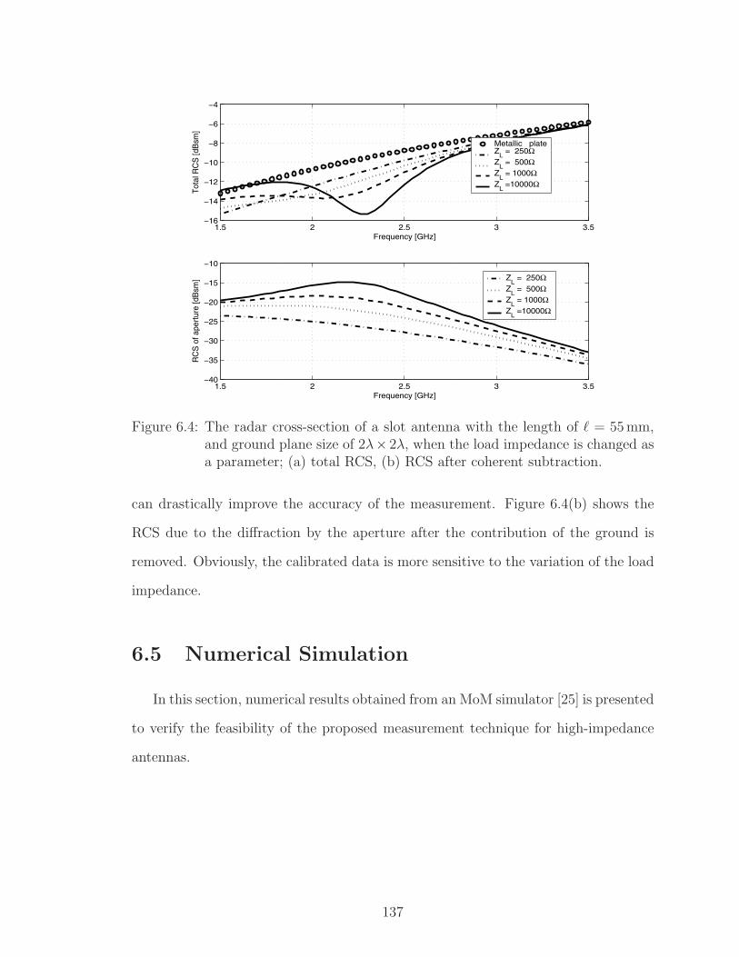
1.5 2 2.5 3 3.5−16
−14
−12
−10
−8
−6
−4
Frequency [GHz]
Tot
al R
CS
[dB
sm]
Metallic plateZ
L = 250Ω
ZL = 500Ω
ZL = 1000Ω
ZL =10000Ω
1.5 2 2.5 3 3.5−40
−35
−30
−25
−20
−15
−10
Frequency [GHz]
RC
S o
f ape
rtur
e [d
Bsm
] ZL = 250Ω
ZL = 500Ω
ZL = 1000Ω
ZL =10000Ω
Figure 6.4: The radar cross-section of a slot antenna with the length of = 55 mm,and ground plane size of 2λ× 2λ, when the load impedance is changed asa parameter; (a) total RCS, (b) RCS after coherent subtraction.
can drastically improve the accuracy of the measurement. Figure 6.4(b) shows the
RCS due to the diffraction by the aperture after the contribution of the ground is
removed. Obviously, the calibrated data is more sensitive to the variation of the load
impedance.
6.5 Numerical Simulation
In this section, numerical results obtained from an MoM simulator [25] is presented
to verify the feasibility of the proposed measurement technique for high-impedance
antennas.
137
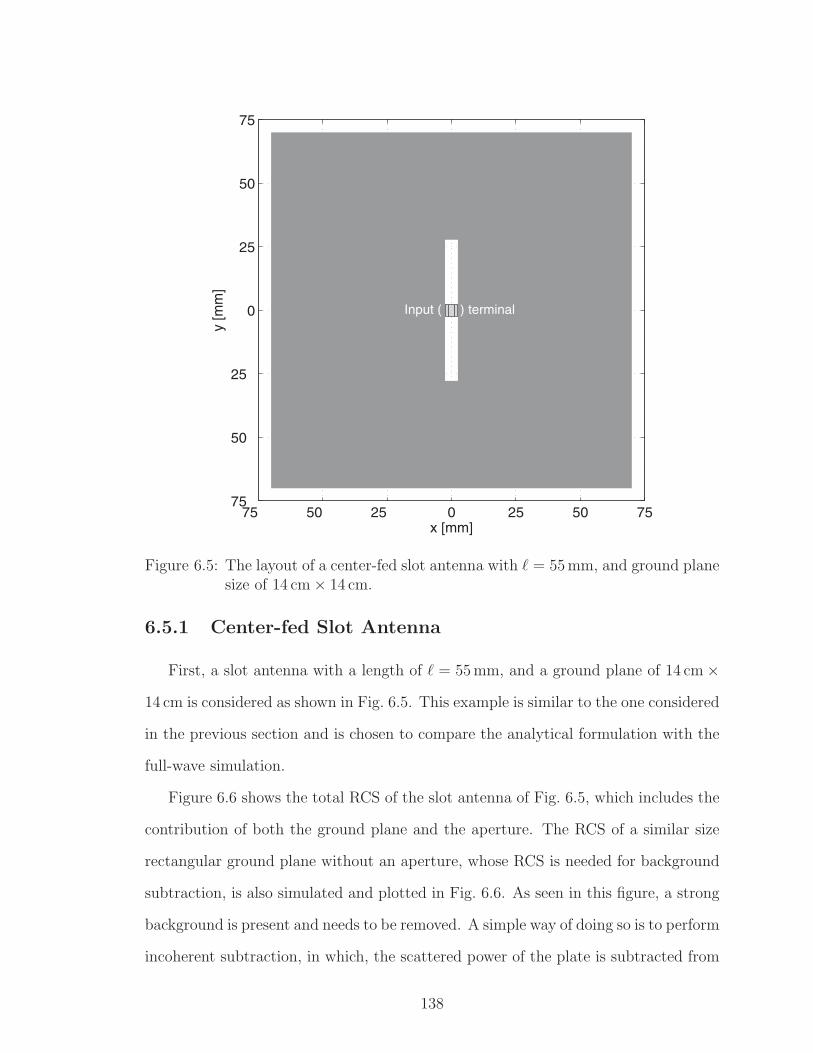
75 50 25 0 25 50 7575
50
25
0
25
50
75
x [mm]
y [m
m]
Input ( ) terminal
Figure 6.5: The layout of a center-fed slot antenna with = 55 mm, and ground planesize of 14 cm × 14 cm.
6.5.1 Center-fed Slot Antenna
First, a slot antenna with a length of = 55 mm, and a ground plane of 14 cm ×14 cm is considered as shown in Fig. 6.5. This example is similar to the one considered
in the previous section and is chosen to compare the analytical formulation with the
full-wave simulation.
Figure 6.6 shows the total RCS of the slot antenna of Fig. 6.5, which includes the
contribution of both the ground plane and the aperture. The RCS of a similar size
rectangular ground plane without an aperture, whose RCS is needed for background
subtraction, is also simulated and plotted in Fig. 6.6. As seen in this figure, a strong
background is present and needs to be removed. A simple way of doing so is to perform
incoherent subtraction, in which, the scattered power of the plate is subtracted from
138
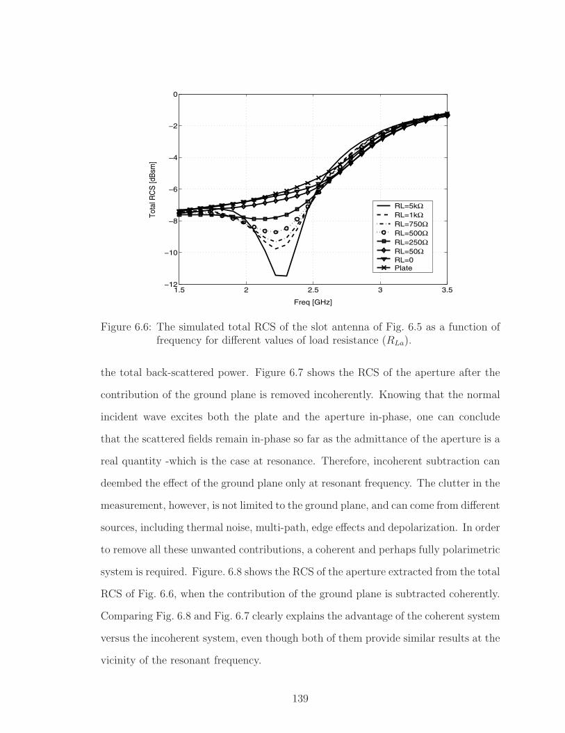
1.5 2 2.5 3 3.5−12
−10
−8
−6
−4
−2
0
Freq [GHz]
Tota
l RC
S [d
Bsm
]
RL=5kΩRL=1kΩRL=750ΩRL=500ΩRL=250ΩRL=50ΩRL=0Plate
Figure 6.6: The simulated total RCS of the slot antenna of Fig. 6.5 as a function offrequency for different values of load resistance (RLa).
the total back-scattered power. Figure 6.7 shows the RCS of the aperture after the
contribution of the ground plane is removed incoherently. Knowing that the normal
incident wave excites both the plate and the aperture in-phase, one can conclude
that the scattered fields remain in-phase so far as the admittance of the aperture is a
real quantity -which is the case at resonance. Therefore, incoherent subtraction can
deembed the effect of the ground plane only at resonant frequency. The clutter in the
measurement, however, is not limited to the ground plane, and can come from different
sources, including thermal noise, multi-path, edge effects and depolarization. In order
to remove all these unwanted contributions, a coherent and perhaps fully polarimetric
system is required. Figure. 6.8 shows the RCS of the aperture extracted from the total
RCS of Fig. 6.6, when the contribution of the ground plane is subtracted coherently.
Comparing Fig. 6.8 and Fig. 6.7 clearly explains the advantage of the coherent system
versus the incoherent system, even though both of them provide similar results at the
vicinity of the resonant frequency.
139
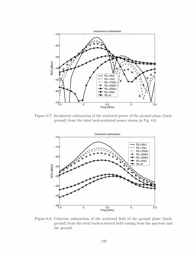
1.5 2 2.5 3 3.5−70
−60
−50
−40
−30
−20
−10
Freq [GHz]
RC
S [d
Bsm
]
Incoherent subtraction
RL=5kΩRL=1kΩRL=750ΩRL=500ΩRL=250ΩRL=50ΩRL=0
Figure 6.7: Incoherent subtraction of the scattered power of the ground plane (back-ground) from the total back-scattered power shown in Fig. 6.6.
1.5 2 2.5 3 3.5−45
−40
−35
−30
−25
−20
−15
−10
Freq [GHz]
RC
S [d
Bsm
]
Coherent subtraction
RL=5kΩRL=1kΩRL=750ΩRL=500ΩRL=250ΩRL=50ΩRL=0
Figure 6.8: Coherent subtraction of the scattered field of the ground plane (back-ground) from the total back-scattered field coming from the aperture andthe ground.
140
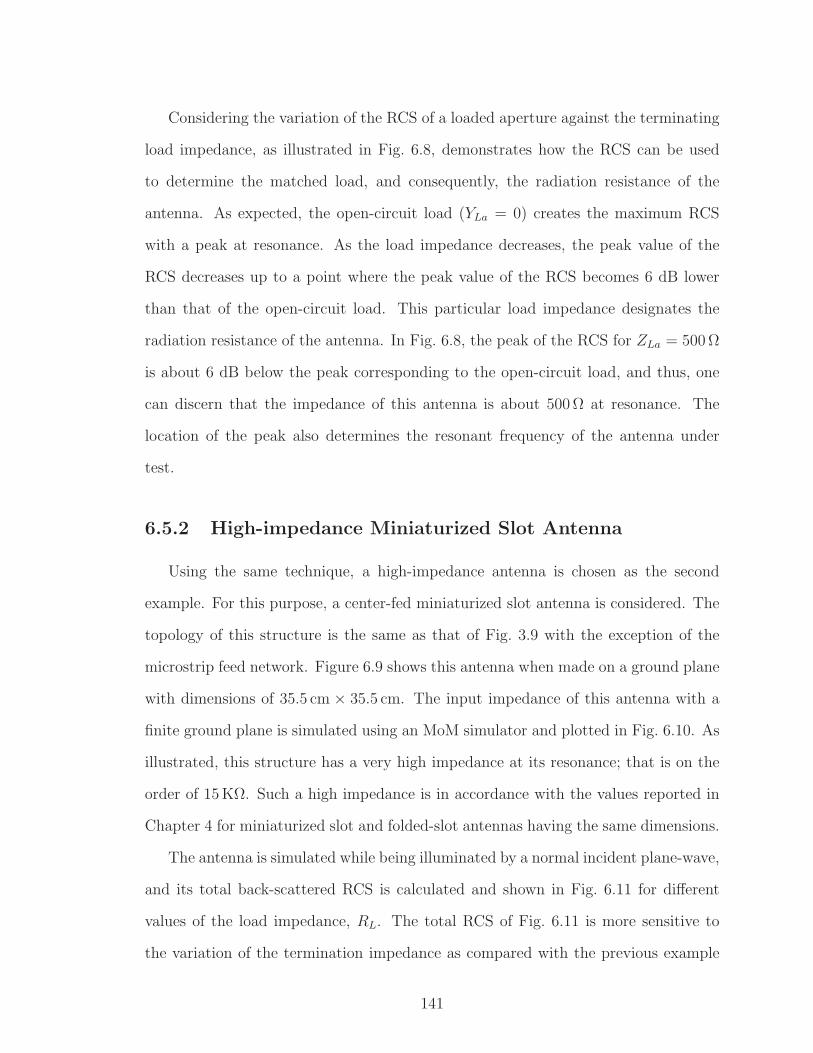
Considering the variation of the RCS of a loaded aperture against the terminating
load impedance, as illustrated in Fig. 6.8, demonstrates how the RCS can be used
to determine the matched load, and consequently, the radiation resistance of the
antenna. As expected, the open-circuit load (YLa = 0) creates the maximum RCS
with a peak at resonance. As the load impedance decreases, the peak value of the
RCS decreases up to a point where the peak value of the RCS becomes 6 dB lower
than that of the open-circuit load. This particular load impedance designates the
radiation resistance of the antenna. In Fig. 6.8, the peak of the RCS for ZLa = 500 Ω
is about 6 dB below the peak corresponding to the open-circuit load, and thus, one
can discern that the impedance of this antenna is about 500 Ω at resonance. The
location of the peak also determines the resonant frequency of the antenna under
test.
6.5.2 High-impedance Miniaturized Slot Antenna
Using the same technique, a high-impedance antenna is chosen as the second
example. For this purpose, a center-fed miniaturized slot antenna is considered. The
topology of this structure is the same as that of Fig. 3.9 with the exception of the
microstrip feed network. Figure 6.9 shows this antenna when made on a ground plane
with dimensions of 35.5 cm × 35.5 cm. The input impedance of this antenna with a
finite ground plane is simulated using an MoM simulator and plotted in Fig. 6.10. As
illustrated, this structure has a very high impedance at its resonance; that is on the
order of 15 KΩ. Such a high impedance is in accordance with the values reported in
Chapter 4 for miniaturized slot and folded-slot antennas having the same dimensions.
The antenna is simulated while being illuminated by a normal incident plane-wave,
and its total back-scattered RCS is calculated and shown in Fig. 6.11 for different
values of the load impedance, RL. The total RCS of Fig. 6.11 is more sensitive to
the variation of the termination impedance as compared with the previous example
141
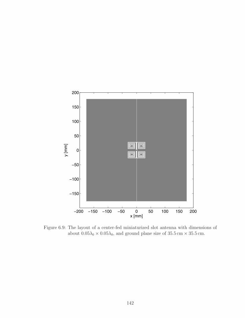
−200 −150 −100 −50 0 50 100 150 200
−150
−100
−50
0
50
100
150
200
x [mm]
y [m
m]
Figure 6.9: The layout of a center-fed miniaturized slot antenna with dimensions ofabout 0.05λ0 × 0.05λ0, and ground plane size of 35.5 cm × 35.5 cm.
142
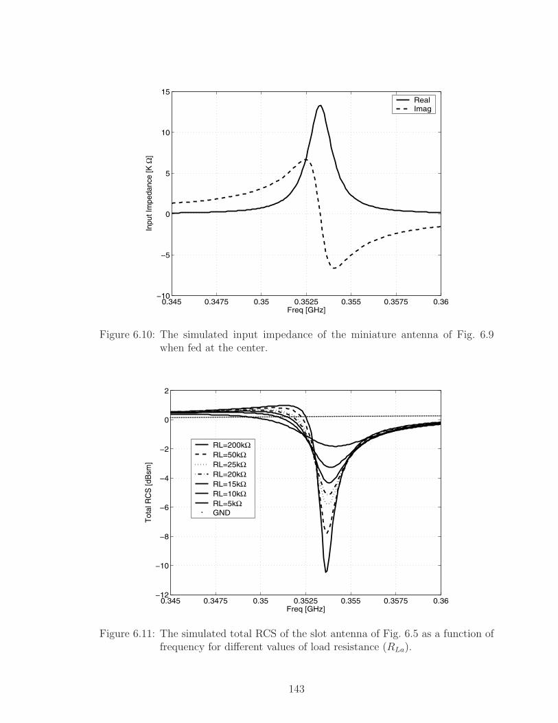
0.345 0.3475 0.35 0.3525 0.355 0.3575 0.36−10
−5
0
5
10
15
Freq [GHz]
Inpu
t Im
peda
nce
[K Ω
]
RealImag
Figure 6.10: The simulated input impedance of the miniature antenna of Fig. 6.9when fed at the center.
0.345 0.3475 0.35 0.3525 0.355 0.3575 0.36−12
−10
−8
−6
−4
−2
0
2
Freq [GHz]
Tot
al R
CS
[dB
sm]
RL=200kΩRL=50kΩRL=25kΩRL=20kΩRL=15kΩRL=10kΩRL=5kΩGND
Figure 6.11: The simulated total RCS of the slot antenna of Fig. 6.5 as a function offrequency for different values of load resistance (RLa).
143
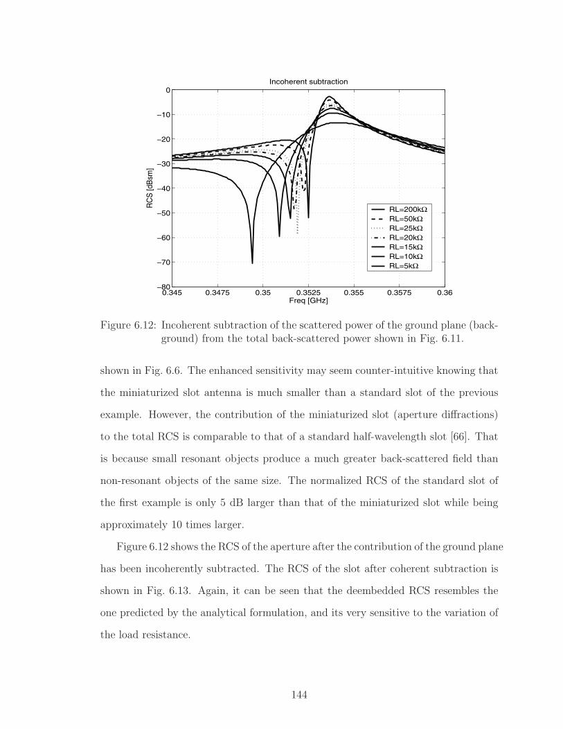
0.345 0.3475 0.35 0.3525 0.355 0.3575 0.36−80
−70
−60
−50
−40
−30
−20
−10
0
Freq [GHz]
RC
S [d
Bsm
]
Incoherent subtraction
RL=200kΩRL=50kΩRL=25kΩRL=20kΩRL=15kΩRL=10kΩRL=5kΩ
Figure 6.12: Incoherent subtraction of the scattered power of the ground plane (back-ground) from the total back-scattered power shown in Fig. 6.11.
shown in Fig. 6.6. The enhanced sensitivity may seem counter-intuitive knowing that
the miniaturized slot antenna is much smaller than a standard slot of the previous
example. However, the contribution of the miniaturized slot (aperture diffractions)
to the total RCS is comparable to that of a standard half-wavelength slot [66]. That
is because small resonant objects produce a much greater back-scattered field than
non-resonant objects of the same size. The normalized RCS of the standard slot of
the first example is only 5 dB larger than that of the miniaturized slot while being
approximately 10 times larger.
Figure 6.12 shows the RCS of the aperture after the contribution of the ground plane
has been incoherently subtracted. The RCS of the slot after coherent subtraction is
shown in Fig. 6.13. Again, it can be seen that the deembedded RCS resembles the
one predicted by the analytical formulation, and its very sensitive to the variation of
the load resistance.
144
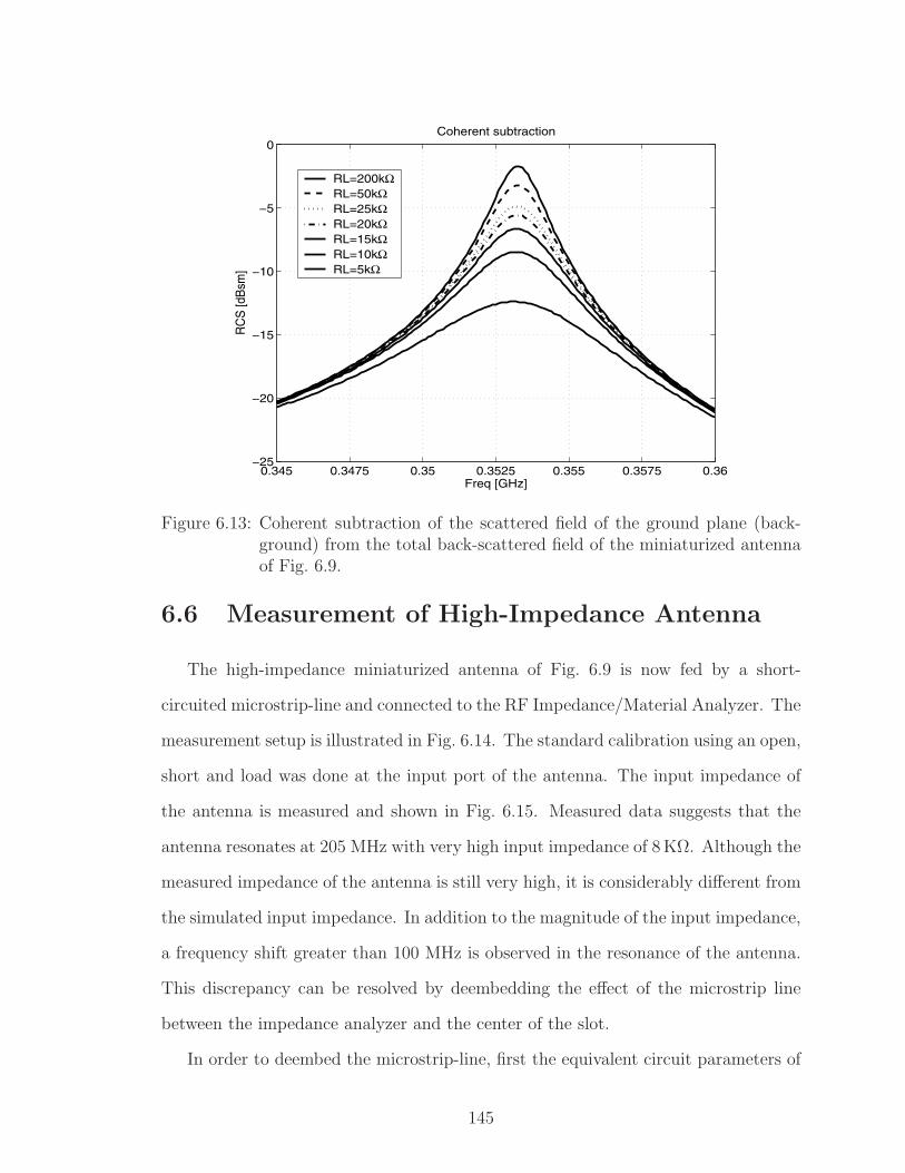
0.345 0.3475 0.35 0.3525 0.355 0.3575 0.36−25
−20
−15
−10
−5
0
Freq [GHz]
RC
S [d
Bsm
]
Coherent subtraction
RL=200kΩRL=50kΩRL=25kΩRL=20kΩRL=15kΩRL=10kΩRL=5kΩ
Figure 6.13: Coherent subtraction of the scattered field of the ground plane (back-ground) from the total back-scattered field of the miniaturized antennaof Fig. 6.9.
6.6 Measurement of High-Impedance Antenna
The high-impedance miniaturized antenna of Fig. 6.9 is now fed by a short-
circuited microstrip-line and connected to the RF Impedance/Material Analyzer. The
measurement setup is illustrated in Fig. 6.14. The standard calibration using an open,
short and load was done at the input port of the antenna. The input impedance of
the antenna is measured and shown in Fig. 6.15. Measured data suggests that the
antenna resonates at 205 MHz with very high input impedance of 8 KΩ. Although the
measured impedance of the antenna is still very high, it is considerably different from
the simulated input impedance. In addition to the magnitude of the input impedance,
a frequency shift greater than 100 MHz is observed in the resonance of the antenna.
This discrepancy can be resolved by deembedding the effect of the microstrip line
between the impedance analyzer and the center of the slot.
In order to deembed the microstrip-line, first the equivalent circuit parameters of
145
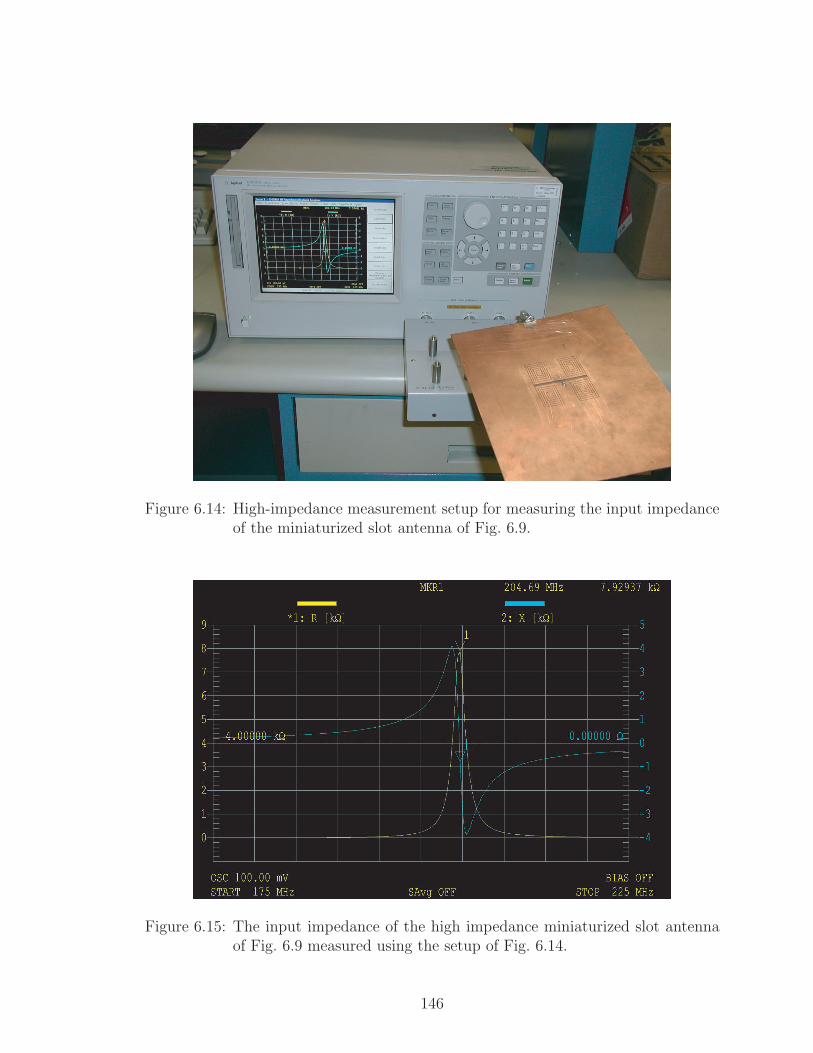
Figure 6.14: High-impedance measurement setup for measuring the input impedanceof the miniaturized slot antenna of Fig. 6.9.
Figure 6.15: The input impedance of the high impedance miniaturized slot antennaof Fig. 6.9 measured using the setup of Fig. 6.14.
146
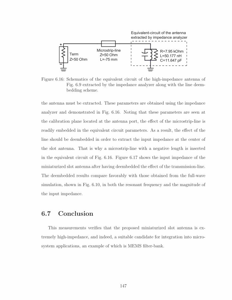
Microstrip-line
L=-75 mmZ=50 Ohm
C=11.647 pFL=50.177 nHR=7.95 kOhm
TermZ=50 Ohm
+
Equivalent-circuit of the antennaextracted by impedance analyzer
Figure 6.16: Schematics of the equivalent circuit of the high-impedance antenna ofFig. 6.9 extracted by the impedance analyzer along with the line deem-bedding scheme.
the antenna must be extracted. These parameters are obtained using the impedance
analyzer and demonstrated in Fig. 6.16. Noting that these parameters are seen at
the calibration plane located at the antenna port, the effect of the microstrip-line is
readily embedded in the equivalent circuit parameters. As a result, the effect of the
line should be deembedded in order to extract the input impedance at the center of
the slot antenna. That is why a microstrip-line with a negative length is inserted
in the equivalent circuit of Fig. 6.16. Figure 6.17 shows the input impedance of the
miniaturized slot antenna after having deembedded the effect of the transmission-line.
The deembedded results compare favorably with those obtained from the full-wave
simulation, shown in Fig. 6.10, in both the resonant frequency and the magnitude of
the input impedance.
6.7 Conclusion
This measurements verifies that the proposed miniaturized slot antenna is ex-
tremely high-impedance, and indeed, a suitable candidate for integration into micro-
system applications, an example of which is MEMS filter-bank.
147
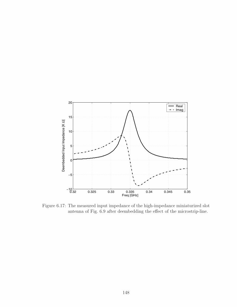
0.32 0.325 0.33 0.335 0.34 0.345 0.35−10
−5
0
5
10
15
20
Freq [GHz]
Dee
mbe
dded
Inpu
t Im
peda
nce
[K Ω
]
RealImag
Figure 6.17: The measured input impedance of the high-impedance miniaturized slotantenna of Fig. 6.9 after deembedding the effect of the microstrip-line.
148

CHAPTER 7
Conclusions and Recommendations for Future
Work
7.1 Summary
The main objective of this thesis was to address the challenging issue of antenna
and microwave filter miniaturization in the context of wireless systems. The size
of antennas and filters, as well as any other resonant components, is tightly depen-
dant upon the physical dimensions of the structure. In order to establish standing
electromagnetic waves, the dimension of the resonant structure needs to be at least
half a wavelength, which imposes a size limitation. Furthermore, the size of these
components critically affects the power efficiency and ohmic losses. The aforemen-
tioned issues have so far precluded antennas and perhaps microwave filters from being
integrated monolithically into the rest of the transceiver circuitry.
In response to the above need, a novel approach for miniaturization of anten-
nas and filters have been proposed. In addition to miniaturization, high-impedance
matching of the miniaturized antennas was investigated. In fact, high-impedance is
another important requirement that must be fulfilled before integrating antennas into
high-impedance electronics and microsystems becomes a reality.
149

7.2 Contributions
The major contributions of this thesis fall into three different categories:
7.2.1 Antenna Miniaturization
The concept of a new class of efficient miniaturized planar slot antennas with a
potential for reconfigurability was demonstrated. This approach takes advantage of
the antenna topology to achieve miniaturization. Using this concept, the design of a
miniaturized antenna as small as 0.05λ0×0.05λ0 with a fairly high gain of −3 dBi was
demonstrated. This antenna is an order of magnitude smaller than the standard half-
wavelength antennas. Since there are neither polarization nor mismatch losses, the
antenna efficiency is limited only by the dielectric and ohmic losses of the substrate
on which the antenna is made. The proposed topology can also be made on a high
dielectric constant substrate/superstrate providing further size reduction.
7.2.2 Bandwidth Enhancement of Miniaturized Antennas
The bandwidth of this new generation of antennas is rather small as is the case
for all small antennas. Resonant antennas in general, and slot-dipoles in particular,
are inherently narrow-band. By reducing the size of the slot, the physical aperture
of the antenna is reduced, and therefore, the radiation conductance of a miniatur-
ized slot antenna becomes very small. One way to match the high impedance of the
miniaturized slot antenna to a 50 Ω line is to tune it slightly off resonance, whether
capacitively or inductively. A smaller capacitance or larger inductance is needed de-
pending on whether the antenna is tuned below or above the resonance. However,
a smaller capacitance, or conversely a larger inductance, results in a narrower band-
width. To partially improve the bandwidth of miniaturized slot antennas, one can
increase the physical aperture without increasing the overall size of the antenna by
150

introducing folded topology. Some other miniature antenna topologies, such as com-
plementary and self-complementary realizations of the miniature folded slot structure,
were explored as suitable candidates for further bandwidth improvement.
7.2.3 Microwave Filter Miniaturization
A similar approach to the one used for designing miniaturized antennas can be
applied to other passive microwave components, such as resonators, band-pass filters,
couplers, and so on. As part of the filter miniaturization efforts, a new class of low in-
sertion loss miniaturized filters using slot-line resonators is proposed. Miniaturization
is achieved by terminating the slot-line with a double-spiral inductive termination at
both ends. Using these miniaturized resonators, both positive and negative couplings
may be realized, and therefore, both standard coupled-line and cross-coupled quasi-
elliptic filters are realizable. The unloaded Q of these slot-line filters is considerably
higher than that of miniaturized microstrip filters of comparable dimensions due to
the inherent higher Q of slot-line. The resonators/filters that have been introduced
are, again, about an order of magnitude smaller than their standard distributed coun-
terparts, while still having comparable or even higher quality factors.
7.2.4 High-Impedance Antenna Measurement
Another aspect of this research is its potential for integration with emerging
transceiver designs based on micro-electromechanical systems (MEMS). In order to in-
tegrate these miniature antennas with the rest of the transceiver circuitry, impedance
matching and interfacing issues must be resolved. Usually, MEMS filters have very
high terminating impedance (15 KΩ) and cannot be connected directly to 50 Ω anten-
nas. It is importnat to note that traditional impedance-matching techniques are not
able to overcome this difficulty. Thus, new methodologies should be investigated to
make high-impedance miniaturized antennas. One method investigated in this work
151

is to reduce the physical aperture of the antenna to make its impedance closer to
those impedances appropriate for MEMS filters. This step is considered a significant
milestone towards the fabrication of the whole transceiver on a single chip knowing
that the antenna imposes a stringent bottleneck on the overall size of the wireless
subsystems.
7.3 Future Work
In addition to wireless microsystems, which have enormous overlap with the main
course of this research, there are some other multidisciplinary areas, such as biotech-
nology, and nanotechnology that this work can significantly contribute. There are
three distinct features in this research that can be applied to the aforementioned
areas. First, the need for miniature RF and electromagnetic passive components
is inevitable (miniaturization). Second, low-power requirements of these structures
demand a great deal of effort to maintain the losses of miniature structures as low
as possible, especially at higher frequencies (high Q, and low loss). Third, the high
impedance nature of micro- and nano-scale devices calls for high-impedance minia-
ture antenna/microwave circuit structures for integration. The high-impedance char-
acteristic ensures that the power consumption of the system will be at minimum
(high-impedance). The following discussion, more specifically, outlines some of the
interesting venues in which this research can be pursued in future.
Fabrication of Miniaturized Antennas on Meta-Materials
Engineering high-performance magneto-dielectric materials (Meta-Materials) has
created a new avenue for RF engineering research. This new generation of materials
has great potential to be used as substrates for novel antennas and microwave circuits.
Suppressing the surface waves, controlling the near field couplings, manipulating the
152
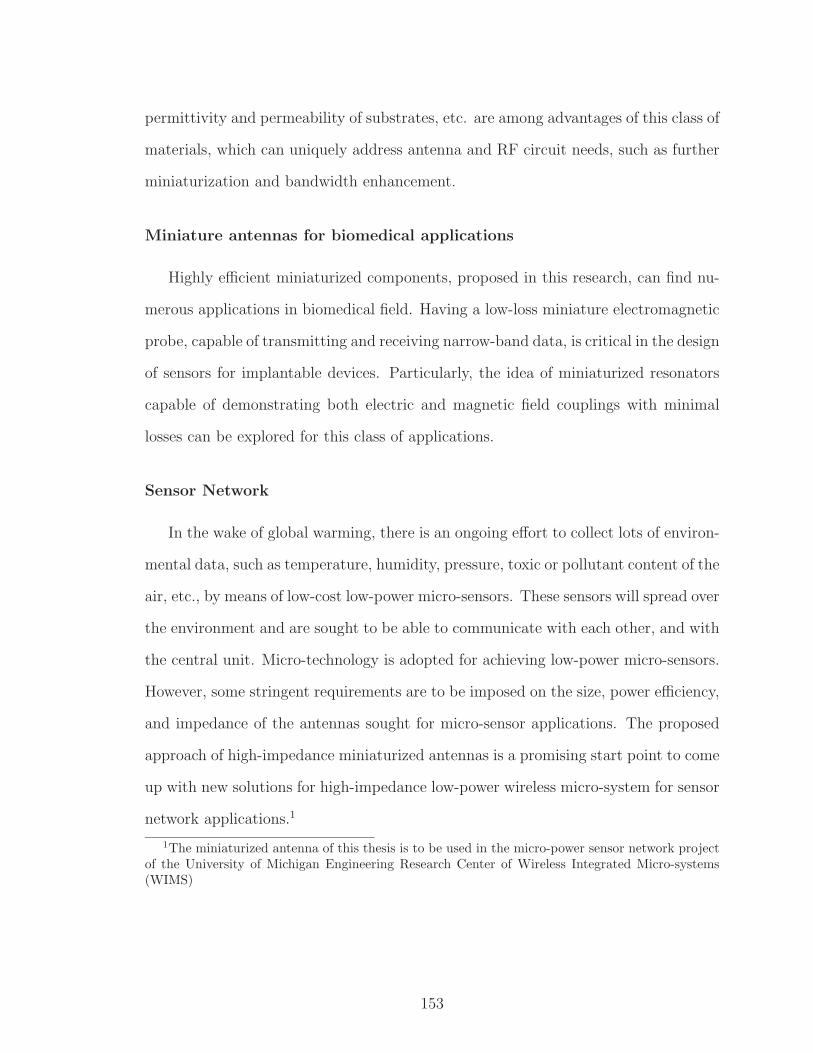
permittivity and permeability of substrates, etc. are among advantages of this class of
materials, which can uniquely address antenna and RF circuit needs, such as further
miniaturization and bandwidth enhancement.
Miniature antennas for biomedical applications
Highly efficient miniaturized components, proposed in this research, can find nu-
merous applications in biomedical field. Having a low-loss miniature electromagnetic
probe, capable of transmitting and receiving narrow-band data, is critical in the design
of sensors for implantable devices. Particularly, the idea of miniaturized resonators
capable of demonstrating both electric and magnetic field couplings with minimal
losses can be explored for this class of applications.
Sensor Network
In the wake of global warming, there is an ongoing effort to collect lots of environ-
mental data, such as temperature, humidity, pressure, toxic or pollutant content of the
air, etc., by means of low-cost low-power micro-sensors. These sensors will spread over
the environment and are sought to be able to communicate with each other, and with
the central unit. Micro-technology is adopted for achieving low-power micro-sensors.
However, some stringent requirements are to be imposed on the size, power efficiency,
and impedance of the antennas sought for micro-sensor applications. The proposed
approach of high-impedance miniaturized antennas is a promising start point to come
up with new solutions for high-impedance low-power wireless micro-system for sensor
network applications.1
1The miniaturized antenna of this thesis is to be used in the micro-power sensor network projectof the University of Michigan Engineering Research Center of Wireless Integrated Micro-systems(WIMS)
153
High-Impedance Miniature Antennas and Micro/Nano-scale Devices
Micro- and nano-scale devices are generally very high-impedance mainly due to
their small sizes. A few examples of such devices, including MEMS filter banks
and CNT transistors, have already been mentioned in this thesis. In order for mi-
cro/nanodevices to be utilized in future wireless systems, it is necessary to resolve the
impedance mismatch between them and the antenna system. Introducing the idea
of high-impedance miniaturized antennas can be found amenable to the impedance
mismatch of these devices.
154

APPENDIX
155

APPENDIX A
Effects of the Finite Ground Plane on the Slot
Antenna Radiation Pattern
A.1 Introduction
A slot antenna element is constructed by cutting slots into a perfectly conduct-
ing ground plane of an infinite extent. Figure A.1 illustrates a slot antenna at the
resonance fed at the center by a two-wire transmission line. For a narrow slot, the
slot itself can be considered as a section of a two-wire transmission line terminated
at both ends by short-circuits. A standing wave of voltage can be established across
the slot-line such that the electric field in the slot is approximately given by
Ey(z) =Vab
wcos
2π
λs
z (A.1)
where Vab is the peak voltage at the center. The equivalence principle can be applied
to replace the electric field across the slot-line with an equivalent magnetic current.
This magnetic current radiates at the presence of the ground. Provided that the
ground plane is of an infinite extent, image theory reduces all the sources to a linear
156
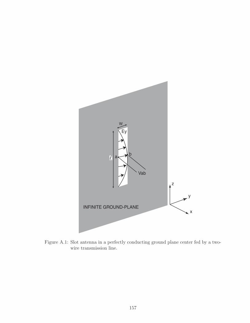
y
x
z
a b
Vab
Ey
INFINITE GROUND-PLANE
W
Figure A.1: Slot antenna in a perfectly conducting ground plane center fed by a two-wire transmission line.
157
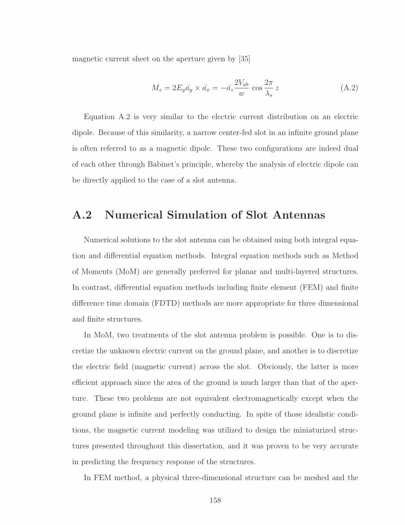
magnetic current sheet on the aperture given by [35]
Mz = 2Eyay × ax = −az2Vab
wcos
2π
λs
z (A.2)
Equation A.2 is very similar to the electric current distribution on an electric
dipole. Because of this similarity, a narrow center-fed slot in an infinite ground plane
is often referred to as a magnetic dipole. These two configurations are indeed dual
of each other through Babinet’s principle, whereby the analysis of electric dipole can
be directly applied to the case of a slot antenna.
A.2 Numerical Simulation of Slot Antennas
Numerical solutions to the slot antenna can be obtained using both integral equa-
tion and differential equation methods. Integral equation methods such as Method
of Moments (MoM) are generally preferred for planar and multi-layered structures.
In contrast, differential equation methods including finite element (FEM) and finite
difference time domain (FDTD) methods are more appropriate for three dimensional
and finite structures.
In MoM, two treatments of the slot antenna problem is possible. One is to dis-
cretize the unknown electric current on the ground plane, and another is to discretize
the electric field (magnetic current) across the slot. Obviously, the latter is more
efficient approach since the area of the ground is much larger than that of the aper-
ture. These two problems are not equivalent electromagnetically except when the
ground plane is infinite and perfectly conducting. In spite of those idealistic condi-
tions, the magnetic current modeling was utilized to design the miniaturized struc-
tures presented throughout this dissertation, and it was proven to be very accurate
in predicting the frequency response of the structures.
In FEM method, a physical three-dimensional structure can be meshed and the
158
fields are solved for. In this approach, there is no restriction on the modeling of a
finite ground plane and other physical parameters of the problem. But this approach
was shown to be numerically cumbersome for simulating the miniaturized structures
having a very large aspect ratio. When the aspect ratio is large, very fine griding
is required which necessitates exorbitant amount of memory. That is why the MoM
with magnetic current discretization was adopted in this thesis.
The magnetic current discretization has been implemented in some commercially
available MoM softwares such as IE3D [25], in which the magnetic current is treated
as an unknown parameter, and it is solved for using the integral equation method.
The replacement of the slot with an unknown magnetic current element is based on
the presumption that the ground plane should be a perfect conductor and infinite. In
addition to the infinite ground, the dielectric substrate of the antenna is assumed to
be of an infinite extent. Obviously, the simulated results based on these presumptions
do not include ohmic losses of the ground, which is the major source of losses in the
slot antenna. As a result, the radiation efficiency obtained by the magnetic current
simulation is not accurate, and it includes only the dielectric loss of the antenna. Fur-
thermore, ignoring the ohmic loss of the ground leads to some discrepancies between
the simulated and measured bandwidths. In different chapters of this thesis, the issue
of ground plane loss and its effect on the discrepancies between the simulated and
measured results was discussed in details and is not revisited in this appendix.
The application of magnetic current discretization, however, has another impli-
cation, that is the unrealistic presumption of infinite ground plane and substrate.
Therefore, some discrepancies might be expected when measured radiation patterns
(finite ground) are compared with those obtained by the magnetic current simulation
(infinite ground).
The effect of ground plane and dielectric truncations on the radiation pattern of
a printed antenna is basically attributed to the near-field and surface-wave diffrac-
159
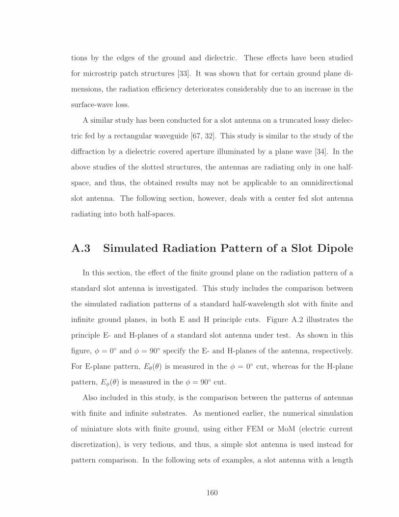
tions by the edges of the ground and dielectric. These effects have been studied
for microstrip patch structures [33]. It was shown that for certain ground plane di-
mensions, the radiation efficiency deteriorates considerably due to an increase in the
surface-wave loss.
A similar study has been conducted for a slot antenna on a truncated lossy dielec-
tric fed by a rectangular waveguide [67, 32]. This study is similar to the study of the
diffraction by a dielectric covered aperture illuminated by a plane wave [34]. In the
above studies of the slotted structures, the antennas are radiating only in one half-
space, and thus, the obtained results may not be applicable to an omnidirectional
slot antenna. The following section, however, deals with a center fed slot antenna
radiating into both half-spaces.
A.3 Simulated Radiation Pattern of a Slot Dipole
In this section, the effect of the finite ground plane on the radiation pattern of a
standard slot antenna is investigated. This study includes the comparison between
the simulated radiation patterns of a standard half-wavelength slot with finite and
infinite ground planes, in both E and H principle cuts. Figure A.2 illustrates the
principle E- and H-planes of a standard slot antenna under test. As shown in this
figure, φ = 0 and φ = 90 specify the E- and H-planes of the antenna, respectively.
For E-plane pattern, Eθ(θ) is measured in the φ = 0 cut, whereas for the H-plane
pattern, Eφ(θ) is measured in the φ = 90 cut.
Also included in this study, is the comparison between the patterns of antennas
with finite and infinite substrates. As mentioned earlier, the numerical simulation
of miniature slots with finite ground, using either FEM or MoM (electric current
discretization), is very tedious, and thus, a simple slot antenna is used instead for
pattern comparison. In the following sets of examples, a slot antenna with a length
160
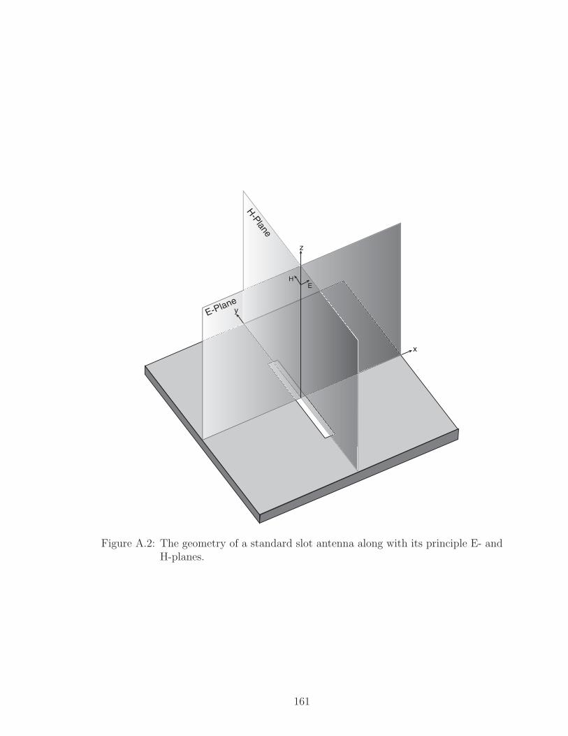
x
y
z
E-Plane
H-Plane
EH
Figure A.2: The geometry of a standard slot antenna along with its principle E- andH-planes.
161
of = 50 mm is simulated. In the case of finite ground plane, the dimensions of the
slot ground plane is set to 100 mm × 100 mm. In cases where the antenna is backed
by a substrate, the dielectric constant of the substrate is selected to be εr = 2.2, with
a thickness of 0.7874 mm.
The first set of examples includes two slot antennas with infinite ground planes,
one with a dielectric substrate and the other without a substrate. To simulate these
problems, IE3D simulator with the magnetic current discretization is utilized. IE3D
can also be used when simulating a finite ground slot but since the moment method
makes use of spectral domain Green’s function, the substrate still has to be infinite.
Therefore, for the case of a slot antenna, with finite ground plane and infinite extent
substrate, IE3D with electric current discretization is used. The finite ground slot
without dielectric can be perfectly simulated using IE3D with electric current. The
same problem can also be solved using a commercially available FEM code, such as
HFSS. Finally, the practical case of a slot with a finite ground and a finite substrate
is simulated using HFSS [68].
Infinite Ground-Plane without Dielectric Substrate
The first example is a slot antenna with an infinite ground plane. In this configu-
ration, no dielectric substrate is used. An infinite ground plane is impossible to mesh,
and therefore, the use of equivalent magnetic currents on the aperture is inevitable.
Figure A.3 shows the radiation pattern of this antenna for both principle E- and H-
planes. This radiation pattern is similar to that of the electric dipole, with E and H
interchanged. That is why the slot on an infinite ground plane is also referred to as
a magnetic dipole, which is indeed, the dual of an electric dipole.
162
−180 −135 −90 −45 0 45 90 135 180−30
−25
−20
−15
−10
−5
0
θ [degree]
Sim
ulat
ed R
adia
tion
Pat
tern
[dB
]
H planeE plane
Figure A.3: The simulated radiation pattern of a slot antenna on air with an infiniteground plane using IE3D with magnetic current discretization.
Infinite Ground-Plane with Infinite Dielectric Substrate
The same structure as previous example, now with a 0.7874 mm thick substrate
with εr = 2.2 is simulated using IE3D, again with magnetic current discretization.
Note that using a Moment Method software (IE3D) implies that the dielectric sub-
strate is also extended to infinity in the x-y plane. The radiation pattern of this
antenna is shown in Fig. A.4. This pattern is similar to the one illustrated in Fig. A.3
with an exception of a slight perturbation of the normal E-field at the dielectric-air
interface –Eθ(θ = 90)– in the E-plane. This perturbation is due to the fact that the
normal electric field is discontinuous at the dielectric interface.
Finite Ground-Plane without Dielectric Substrate
In the next example, a finite ground slot antenna without a dielectric substrate
is considered. This example can be simulated using either MoM with electric cur-
rent discretization or FEM. Figure A.5 demonstrates the radiation patterns of this
163
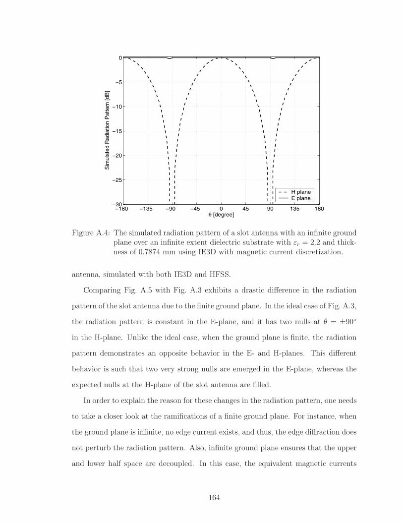
−180 −135 −90 −45 0 45 90 135 180−30
−25
−20
−15
−10
−5
0
θ [degree]
Sim
ulat
ed R
adia
tion
Pat
tern
[dB
]
H planeE plane
Figure A.4: The simulated radiation pattern of a slot antenna with an infinite groundplane over an infinite extent dielectric substrate with εr = 2.2 and thick-ness of 0.7874 mm using IE3D with magnetic current discretization.
antenna, simulated with both IE3D and HFSS.
Comparing Fig. A.5 with Fig. A.3 exhibits a drastic difference in the radiation
pattern of the slot antenna due to the finite ground plane. In the ideal case of Fig. A.3,
the radiation pattern is constant in the E-plane, and it has two nulls at θ = ±90
in the H-plane. Unlike the ideal case, when the ground plane is finite, the radiation
pattern demonstrates an opposite behavior in the E- and H-planes. This different
behavior is such that two very strong nulls are emerged in the E-plane, whereas the
expected nulls at the H-plane of the slot antenna are filled.
In order to explain the reason for these changes in the radiation pattern, one needs
to take a closer look at the ramifications of a finite ground plane. For instance, when
the ground plane is infinite, no edge current exists, and thus, the edge diffraction does
not perturb the radiation pattern. Also, infinite ground plane ensures that the upper
and lower half space are decoupled. In this case, the equivalent magnetic currents
164
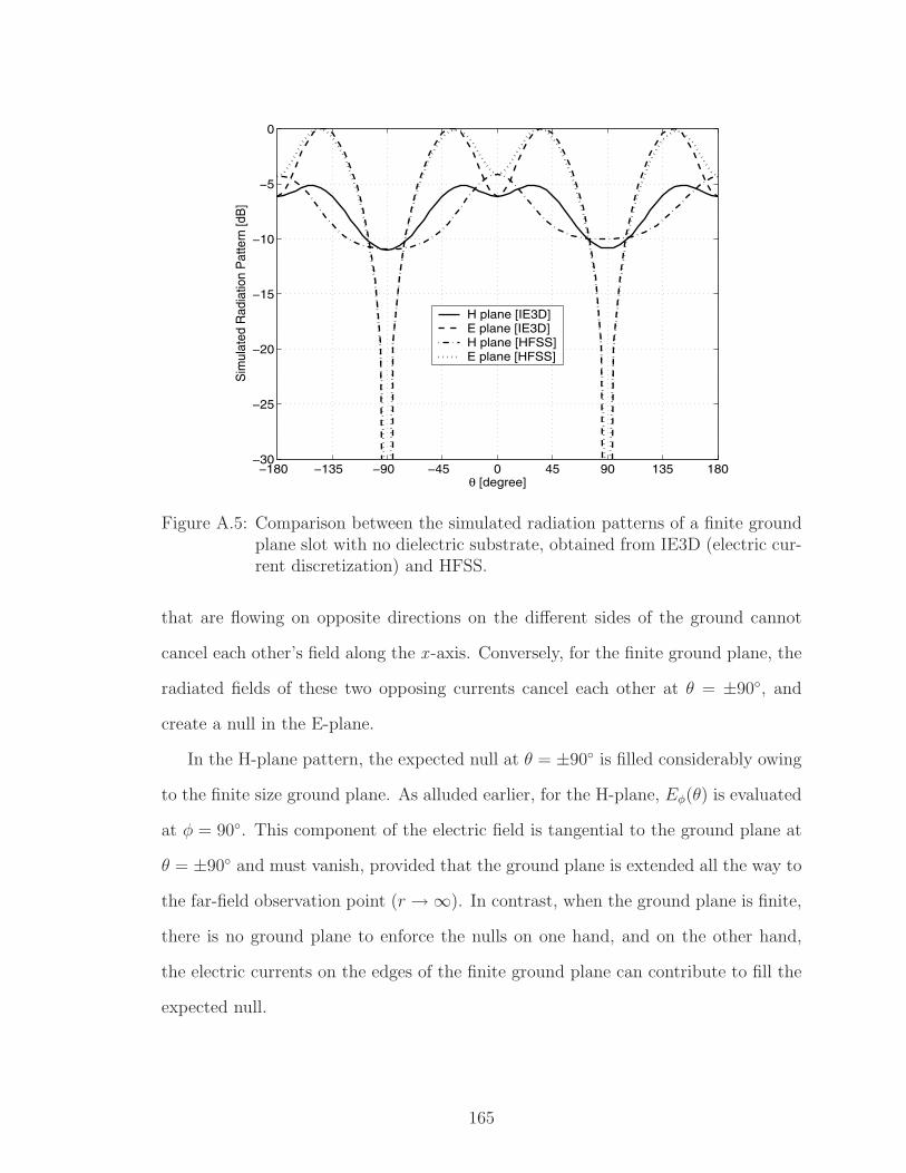
−180 −135 −90 −45 0 45 90 135 180−30
−25
−20
−15
−10
−5
0
θ [degree]
Sim
ulat
ed R
adia
tion
Pat
tern
[dB
]
H plane [IE3D]E plane [IE3D]H plane [HFSS]E plane [HFSS]
Figure A.5: Comparison between the simulated radiation patterns of a finite groundplane slot with no dielectric substrate, obtained from IE3D (electric cur-rent discretization) and HFSS.
that are flowing on opposite directions on the different sides of the ground cannot
cancel each other’s field along the x -axis. Conversely, for the finite ground plane, the
radiated fields of these two opposing currents cancel each other at θ = ±90, and
create a null in the E-plane.
In the H-plane pattern, the expected null at θ = ±90 is filled considerably owing
to the finite size ground plane. As alluded earlier, for the H-plane, Eφ(θ) is evaluated
at φ = 90. This component of the electric field is tangential to the ground plane at
θ = ±90 and must vanish, provided that the ground plane is extended all the way to
the far-field observation point (r → ∞). In contrast, when the ground plane is finite,
there is no ground plane to enforce the nulls on one hand, and on the other hand,
the electric currents on the edges of the finite ground plane can contribute to fill the
expected null.
165
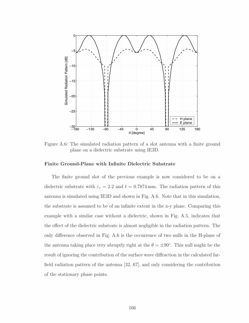
−180 −135 −90 −45 0 45 90 135 180−30
−25
−20
−15
−10
−5
0
θ [degree]
Sim
ulat
ed R
adia
tion
Pat
tern
[dB
]
H planeE plane
Figure A.6: The simulated radiation pattern of a slot antenna with a finite groundplane on a dielectric substrate using IE3D.
Finite Ground-Plane with Infinite Dielectric Substrate
The finite ground slot of the previous example is now considered to be on a
dielectric substrate with εr = 2.2 and t = 0.7874 mm. The radiation pattern of this
antenna is simulated using IE3D and shown in Fig. A.6. Note that in this simulation,
the substrate is assumed to be of an infinite extent in the x-y plane. Comparing this
example with a similar case without a dielectric, shown in Fig. A.5, indicates that
the effect of the dielectric substrate is almost negligible in the radiation pattern. The
only difference observed in Fig. A.6 is the occurrence of two nulls in the H-plane of
the antenna taking place very abruptly right at the θ = ±90. This null might be the
result of ignoring the contribution of the surface wave diffraction in the calculated far-
field radiation pattern of the antenna [32, 67], and only considering the contribution
of the stationary phase points.
166
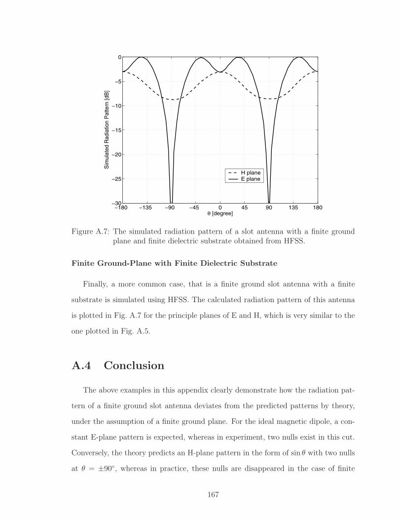
−180 −135 −90 −45 0 45 90 135 180−30
−25
−20
−15
−10
−5
0
θ [degree]
Sim
ulat
ed R
adia
tion
Pat
tern
[dB
]
H planeE plane
Figure A.7: The simulated radiation pattern of a slot antenna with a finite groundplane and finite dielectric substrate obtained from HFSS.
Finite Ground-Plane with Finite Dielectric Substrate
Finally, a more common case, that is a finite ground slot antenna with a finite
substrate is simulated using HFSS. The calculated radiation pattern of this antenna
is plotted in Fig. A.7 for the principle planes of E and H, which is very similar to the
one plotted in Fig. A.5.
A.4 Conclusion
The above examples in this appendix clearly demonstrate how the radiation pat-
tern of a finite ground slot antenna deviates from the predicted patterns by theory,
under the assumption of a finite ground plane. For the ideal magnetic dipole, a con-
stant E-plane pattern is expected, whereas in experiment, two nulls exist in this cut.
Conversely, the theory predicts an H-plane pattern in the form of sin θ with two nulls
at θ = ±90, whereas in practice, these nulls are disappeared in the case of finite
167

ground plane.
Another minor effect in the simulated radiation pattern of a finite ground slot is
the presence of two humps around the boresight. This can also be attributed to the
the radiation by the edges whose radiation is slightly out of phase with that of the
main slot, and consequently, the overall radiation pattern resembles beam steering
property of a phased array. The features of these humps, as well as their locations
change with respect to the ground plane size.
Knowing that the radiation pattern of an infinitesimal dipole is very similar to that
of a half-wave dipole, the results of this study hold for the miniaturized antennas, and
therefore, explain the discrepancies between the simulated and measured radiation
patterns of the antennas of Chapter 2, and Chapter 3.
168

BIBLIOGRAPHY
169

BIBLIOGRAPHY
[1] L. J. Chu, “Physical limitations of omni-directional antennas,” J. Appl. Phys.,vol. 19, pp. 1163–1175, Dec. 1948.
[2] R. C. Hansen, “Fundamental limitations in antennas,” Proceedings of the IEEE,vol. 69, pp. 170–182, Feb. 1981.
[3] R. F. Harrington, “Effect of antenna size on gain, bandwidth, and efficiency,”J. Res. Natl. Bur. Std., vol. 64D, pp. 1–12, 1960.
[4] G. L. Matthaei, L. Young, and E. M. T. Jones, Microwave Filters, Impedance-Matching Networks and Coupling Structures, McGraw-Hill, New York, 1964.
[5] R. Levy, R. V. Snyder, and G. L. Matthaei, “Design of microwave filters,” IEEETrans. Microwave Theory Tech., vol. 50, pp. 783–793, Mar. 2002.
[6] R. R. Mansour, “Microwave superconductivity,” IEEE Trans. Microwave TheoryTech., vol. 50, pp. 750–759, Mar. 2002.
[7] H. T. Su, F. Huang, and M. J. Lancaster, “Highly miniature HTS microwavefilters,” IEEE Trans. Applied Superconductivity., vol. 11, pp. 349–352, Mar. 2001.
[8] H. A. Wheeler, “Fundamental limitations of small antennas,” Proceedings of theI.R.E., vol. 35, pp. 1479–1484, Dec. 1947.
[9] H. A. Wheeler, “Small antennas,” IEEE Trans. Antennas Propagat., vol. 23, pp.462–469, Jul. 1975.
[10] R. E. Collin, “Small antennas,” IEEE Trans. Antennas Propagat., vol. 12, pp.23–27, Jan. 1966.
[11] J. A. Kaiser, “The Archimedean two-wire spiral antenna,” I.R.E. Trans. Anten-nas Propagat., vol. 8, pp. 312–323, May. 1960.
[12] Em-Picasso, Electromagnetic Simulation, EMAG Technologies, Inc., Ann Arbor,MI.
[13] J. Rashed, and C. T. Tai, “A new class of Resonant antennas,” IEEE Trans.Antennas Propagat., vol. 39, pp. 1428–1430, Sep. 1991.
170

[14] J. M. Kim, J. G. Yook, W. Y. Song, Y. J. Yoon, J. Y. Park, and H. K. Park,“Compact meander-type slot antennas,” Proceedings of the IEEE AP-S Sympo-sium, vol. 2, pp. 724–727, 2001.
[15] L. P. Ivrissimtzis, M. J. Lancaster, and M. Esa, “Miniature super conductingcoplanar strip antennas for microwave and mm-wave applications,” Proceedingsof the IEEE AP-S Symposium, vol. 1, pp. 391–395, Apr. 1995.
[16] L. P. Ivrissimtzis, M. J. Lancaster, T. S. M. Maclean, and N. Alford, “High-gainseries fed printed dipole arrays made of high-T superconductors,” IEEE Trans.Antennas Propagat., vol. 42, pp. 1419–1429, Oct. 1994.
[17] K. Noguchi, N. Yasui, M. Mizusawa, S. Betsudan, and T. Katagi, “Increasingthe bandwidth of a two-strip meander-line antenna mounted on a conductingbox,” Proceedings of the IEEE AP-S Symposium, vol. 4, pp. 112–115, 2001.
[18] H. Chaloupka, N. Klein, M. Peiniger, H. Piel, A. Pischke, and G. Splitt, “Minia-turized high-temperature superconductor microstrip patch antenna,” IEEETrans. Microwave Theory Tech., vol. 39, pp. 1513–1521, Sep. 1991.
[19] Y.-P. Zhang, T.K.-C. Lo, and Y.-M. Hwang, “A dielectric-loaded miniatureantenna for micro-cellular and personal communications,” Proceedings of theIEEE AP-S Symposium, vol. 2, pp. 1152–1155, 1995.
[20] Y. Hwang Y.P. Zhang, K.M. Luk, and, E.K.N. Yung, “Gain-enhanced minia-turised rectangular dielectric resonator antenna,” Electronics Letters, vol. 33,pp. 350–352, Feb. 1997.
[21] R.E. Collin, Antennas and Radiowave Propagation, McGraw-Hill, New York,1985.
[22] B. K. Kormanyos, W. Harokopus, L. Katehi, and G. Rebeiz, “CPW-fed activeslot antennas,” IEEE Trans. Microwave Theory Tech., vol. 42, pp. 541–545, Apr.1994.
[23] S. Sierra-Garcia and J. Laurin, “Study of a CPW Inductively Coupled SlotAntenna,” IEEE Trans. Antennas Propagat., vol. 47, pp. 58–64, Jan. 1999.
[24] RT/duroid 5880, High Frequency Laminate, Rogers Corporation, AdvancedCircuit Materials Division, Chandler, AZ.
[25] IE3D, Electromagnetic Simulation and Optimization Package, ver. 10.0, ZelandSoftware, Inc., Fremont, CA.
[26] K.C. Gupta, P. Garg, I. Bahl, and P. Bhartia, Microstrip Lines and Slotlines,Artec House, 2nd edition, 1996.
[27] H.G. Akhavan, and D. Mirshekar-Syahkal, “Approximate model for microstripfed slot antennas,” Electronics Letters, vol. 30, pp. 1902–1903, Nov. 1994.
171

[28] M. Fariana, and T. Rozzi, “A short-open deembedding technique for method-of-moments-based electromagnetic analyses,” IEEE Trans. Microwave TheoryTech., vol. 49, pp. 624–628, Apr. 2001.
[29] L. Zhu, and K. Wu, “Unified equivalent-circuit model of planar discontinuitiessuitable for field theory-based CAD and optimization of M(H)MIC’s,” IEEETrans. Microwave Theory Tech., vol. 47, pp. 1589–1602, Sep. 1999.
[30] L. Zhu, and K. Wu, “Complete circuit model of microstrip-fed Slot radiator:Theory and experiments,” IEEE Microwave and Guided Wave Letters, vol. 9,pp. 305–307, Aug. 1999.
[31] J. M. Johnson, and Y. Rahmat-Samii, “Genetic algorithms in engineering elec-tromagnetics,” IEEE Antennas Propagat. Magazine, vol. 39, No. 4, pp. 7–21,Aug. 1997.
[32] B. Stockbroeckx, I. Huynen, and A. Vander Vorst, “Effect of surface wave diffrac-tion on radiation pattern of slot antenna etched in finite ground plane,” Elec-tronics Letters, vol. 36, pp. 1444–1446, Aug. 2000.
[33] A. K. Bhattacharyya, “Effects of ground plane and dielectric truncation on theefficiency of a printed structure,” IEEE Trans. Antennas Propagat., vol. 39, pp.303–308, Mar. 1991.
[34] C. A. Balanis, Antenna Theory: Analysis and Design, John Wiley & Sons, NewYork, 1997.
[35] R. S. Elliott, Antenna Thory and Design, John Wiley, New Jersey, 2003.
[36] K. V. Pugilia, “Application notes: Electromagnetic simulation of some commonbalun structures,” IEEE Microwave Mag., pp. 56–61, Sep. 2002.
[37] Y. Mushiake, Self-Complementary Antennas, Springer-Verlag, New York.
[38] T. Ishizone, Y. Mushiake, “A self-complementary antenna composed of unipoleand notch antennas,” Proceedings of the IEEE AP-S Symposium.
[39] P. Xu, k. Fujimoto, L. Shiming, “Performance of quasi-self-complementary an-tenna using a monopole and a slot,” Proceedings of the IEEE AP-S Symposium.
[40] P. Bradley, R. Ruby, J. D. Larson, Y. Oshmyansky, D. Figueredo, “A film bulkacoustic resonator (FBAR) duplexer for USPCS handset applications,” IEEEMTT-S Int. Microwave Symp. Dig., vol. 1, pp. 367–370, May 2001.
[41] A. Gopinath, A. F. Thomson, and I. M. Stephenson, “Equivalent circuit pa-rameters of microstrip step change in width and cross junction,” IEEE Trans.Microwave Theory Tech., vol. 24, pp. 142–144, Mar. 1976.
[42] M. Makimoto and S. Yamashita, “Compact bandpass filters using steppedimpedance resonators,” Proceedings of the IEEE, vol. 67, pp. 16–19, Jan. 1979.
172

[43] E. G. Cristal, S. Frankel, “Hairpin-line and hybrid hairpinline/half-wave parallelcoupled-line filters,” IEEE Trans. Microwave Theory Tech., vol. 20, pp. 719–728,Nov. 1972.
[44] M. Sagawa, K. Takahashi, and M. Makimoto, “Miniaturized hairpin resonatorfilters and their application to receiver front-end MIC’s,” IEEE Trans. MicrowaveTheory Tech., vol. 37, pp. 1991–1997, Dec. 1989.
[45] S. Y. Lee, and C. M. Tsai, “New cross-coupled filter design uning improvedhairpin resonators,” IEEE Trans. Microwave Theory Tech., vol. 48, pp. 2482–2490, Dec. 2000.
[46] J-S. Hong and M. J. Lancaster, “Couplings of microstrip square open-loop res-onators for cross-coupled planar microwave filters,” IEEE Trans. MicrowaveTheory Tech., vol. 44, pp. 2099–2109, Dec. 1996.
[47] J-S. Hong and M. J. Lancaster, “Theory and experiment of novel microstripslow-wave open-loop resonator filters,” IEEE Trans. Microwave Theory Tech.,vol. 45, pp. 2358–2365, Dec. 1997.
[48] J-S. Hong and M. J. Lancaster, “Aperture-coupled microstrip open-loop res-onators and theirapplications to the design of novel microstrip bandpass filters,”IEEE Trans. Microwave Theory Tech., vol. 47, pp. 1848–1855, Sep. 1999.
[49] E. L. Mariani and J. P. Agrios, “Slot-line filters and couplers,” IEEE Trans.Microwave Theory Tech., vol. 18, pp. 1089–1095, Dec. 1970.
[50] D. F.Williams and S. E. Schwarz, “Design and performance of coplanar waveg-uide bandpass filters,” IEEE Trans. Microwave Theory Tech., vol. 31, pp. 558–566, Jul. 1983.
[51] J. K. A. Everard and K. K. M. Cheng, “High-performance direct coupled band-pass filter on coplanar waveguide,” IEEE Trans. Microwave Theory Tech., vol.41, pp. 1568–1573, Sep. 1993.
[52] M. Muraguchi, T. Hirota, A. Minakawa, K. Ohwada, and T. Sugeta, “UniplanarMMIC’s and their applications,” IEEE Trans. Microwave Theory Tech., vol. 36,pp. 1896–1901, Dec. 1988.
[53] T. Hirota, Y. Tarusawa and H. Ogawa, “Uniplanar MMIC hybrids: a proposednew MMIC structure,” IEEE Trans. Microwave Theory Tech., vol. 35, pp. 576–581, June 1987.
[54] T. Tsujiguchi, H. Matsumoto, and T. Nishikawa, “A miniaturized end-coupledbandpass filter using λ/4 hair-pin coplanar resonators,” IEEE MTT-S Int. Mi-crowave Symp. Dig., pp. 829–832, Jun. 1998.
173

[55] K. Yoshida, K. Sashiyama, S. Nishioka, H. Shimakage, and Z. Wang, “Designand performance of miniaturized superconducting coplanar waveguide filters,”IEEE Trans. Applied Superconductivity., vol. 9, pp. 3905–3908, Jun. 1999.
[56] T. Tsujiguchi, H. Matsumoto, and T. Nishikawa, “A miniaturized double-surfaceCPW bandpass filter improved spurious response,” IEEE Trans. MicrowaveTheory Tech., vol. 49, pp. 879–885, May 2001.
[57] J. Sor, Y. Qian, and T. Itoh, “Miniature low-loss CPW periodic structures forfilter applications,” IEEE Trans. Microwave Theory Tech., vol. 49, pp. 2336–2341, Dec. 2001.
[58] E. Yuan, and S. H. Chao, “Unloaded Q measurement: the critical-pointmethod,” IEEE Trans. Microwave Theory Tech., vol. 43, pp. 1983–1986, Aug.1995.
[59] A. E. Atia, A. E. Williams, “Narrow-bandpass waveguide filters,” IEEE Trans.Microwave Theory Tech., vol. 20, pp. 258–265, Apr. 1972.
[60] R. L. Levy, “Filters with single transmission zeroes at real or imaginary fre-quencies,” IEEE Trans. Microwave Theory Tech., vol. 24, pp. 172–181, Apr.1976.
[61] K. T. Jokella, “Narrow-band stripline or microstrip filters with transmissionzeroes at real and imaginary frequencies,” IEEE Trans. Microwave Theory Tech.,vol. 28, pp. 542–547, Jun. 1980.
[62] R. F. Harrington, Time-Harmonic Electromagnetic Fields, John Wiley & Sons,New York, 2001.
[63] J. A. Kong, Electromagnetic Wave Theory, EMW Pub, Cambridge, MA, 2000.
[64] C. A. Balanis, Advanced Engineering Electromagnetics, J. W. Wiley & Sons,New York, 1989.
[65] D. M. Pozar, Microwave Engineering, J. W. Wiley & Sons, New York, 1998.
[66] R. F. Harrington, “Small resonant scatterers and their use for field measure-ments,” I.R.E. Trans. Microwave Theory Tech., vol. MTT-10, pp. 165–174, May1962.
[67] B. Stockbroeckx, and A. Vander Vorst, “Assympotic Green’s function of a surfacemagnetic current element on a perfect electric conductor plane covered by a lossydielectric substrate,” IEEE Trans. Antennas Propagat., vol. 47, pp. 309–316, Feb.1999.
[68] HFSS, High Frequency Structure Simulator, ver. 9.0, Ansoft Corporation, Pitts-burg, PA.
174