Embed Size (px)
Citation preview

High Voltage Wafer Testing in a Production Environment with the HV S540 Parametric Test System
––APPLICATION NOTE
2 | WWW.TEK.COM
High Voltage Wafer Testing in a Production Environment with the HV S540 Parametric Test System
APPLICATION NOTE
Due to the complexities typically associated with high voltage
(HV) wafer-level testing, such as instrumentation setup,
cabling, probing, automation, and safety, on-wafer HV testing
is usually limited to characterization labs or manual benchtop
setups that are separate from a fab’s standard production
workflow. This application note contains implementation
details on the integration of HV testing in a production
environment.
Keithley has developed several measurement techniques
and approaches that enable automated HV wafer level
characterization on multiple pins without sacrificing low
voltage performance or throughput. These techniques
include integration methods that allow sensitive transistor
characterization and low current leakage tests to run in the
same process flow as HV breakdown and HV capacitance
tests. For example, in one automated test sequence, the
transistor Ioff current is measured, followed by the threshold
voltage (Vth) measurement. Next, the drain current (Ion) is
measured when both the gate and drain are biased above
1 kV. Then, capacitance measurements are performed with a
2 kV bias level. Last, breakdown tests are run at 3 kV levels.
Keithley has also developed a run-time open/short/
load impedance compensation technique that supports
making accurate on-wafer HV capacitance measurements.
This application note will explore these and other HV
measurement issues, as well as share results and
experiences in the emerging field of HV wafer-level testing.
Why HV Testing Is NecessaryPower semiconductor transistors are commonly used in
a variety of industries, including home appliances and
automobiles, as well as in various power applications.
Demand for faster, more powerful devices and switches that
can handle more current and voltage will continue to grow.
Materials
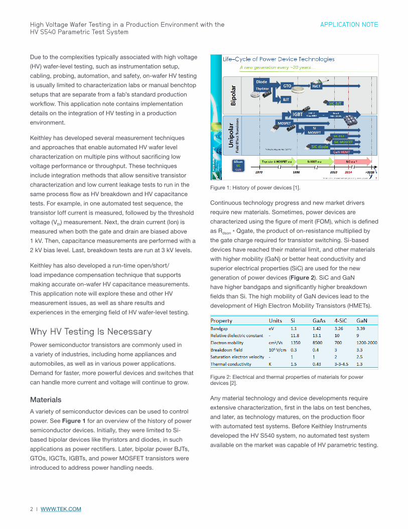
A variety of semiconductor devices can be used to control
power. See Figure 1 for an overview of the history of power
semiconductor devices. Initially, they were limited to Si-
based bipolar devices like thyristors and diodes, in such
applications as power rectifiers. Later, bipolar power BJTs,
GTOs, IGCTs, IGBTs, and power MOSFET transistors were
introduced to address power handling needs.
Figure 1: History of power devices [1].
Continuous technology progress and new market drivers
require new materials. Sometimes, power devices are
characterized using the figure of merit (FOM), which is defined
as Rdson * Qgate, the product of on-resistance multiplied by
the gate charge required for transistor switching. Si-based
devices have reached their material limit, and other materials
with higher mobility (GaN) or better heat conductivity and
superior electrical properties (SiC) are used for the new
generation of power devices (Figure 2). SiC and GaN
have higher bandgaps and significantly higher breakdown
fields than Si. The high mobility of GaN devices lead to the
development of High Electron Mobility Transistors (HMETs).
Figure 2: Electrical and thermal properties of materials for power devices [2].
Any material technology and device developments require
extensive characterization, first in the labs on test benches,
and later, as technology matures, on the production floor
with automated test systems. Before Keithley Instruments
developed the HV S540 system, no automated test system
available on the market was capable of HV parametric testing.
WWW.TEK.COM | 3
High Voltage Wafer Testing in a Production Environment with the HV S540 Parametric Test System
APPLICATION NOTE
HV Characterization Parameters
To offer a clear description of the HV S540 system, it’s
important to understand the parameters typically measured
to characterize power devices. For useful tutorials on power
device characterization parameters, refer to [3], [4] and [5].
Maximum Ratings: V(br)dss, Vgs and Id, Idm
Maximum voltage ratings are defined as the maximum
voltage that can be applied before avalanche breakdown
in the transistor or when the gate is damaged. Vdss is the
maximum voltage between drain (collector) and source, with
the transistor in the off-state. Vgs is the maximum voltage
between gate and the source (emitter) before the gate can be
damaged. The S540 system can perform breakdown tests at
up to 3 kV.
Id is the maximum continuous drain (collector) current that
a device can sustain with no damage. It is controlled by the
Rdson and the thermal power dissipation capability of the DUT.
Idm is the maximum pulse current rating that the device can
handle in the pulse mode. Usually, it is larger than Id and is
determined by the pulse duration and shape.
Idss
This is drain (collector) leakage current of the off-state at a
specified drain voltage. Current usually is small and can be
accurately characterized by the S540 system for Vds up to 3
kV and leakages down to tens of picoamps.
Vgs(th) Threshold Voltage
Threshold voltage measurement for power devices is
the characterization of the off/on transition. Standard Vth
techniques, such as extrapolated Vt (based on maximum
transconductance evaluation), cannot not be used easily here
because of the high current required. Instead, on the S540
system, threshold voltage can be obtained as the gate-to-
source (or gate-to-emitter) voltage, which yields the known
value of the drain (collector) current. The amount of the
critical current varies, and it is based on the characterized
device. Threshold current values as low as 250 µA or 1 mA
are common. For standard LV (low voltage) transistors, trigger
currents between 0.1 µA and 1 µA are commonly used.
Rdson
Probably one of the most important parameters of a power
transistor is Rdson, the drain-to-source resistance in the
on-state. This parameter controls maximum current in the
on-state. Values for Rdson usually are small, in the range of
tens of milliohms, and include not only the resistance of the
channel and drift region, but also, in the test environment,
parasitic resistance of the pads, contact resistance, and
external interconnect resistance. Resistance is measured
at relatively small drain voltages (< 20 V) as a function of
drain current. Drain current can be as high as several tens of
amps, depending on the application. With the S540 system,
Rdson is measured using a Model 2636B SMU SourceMeter®
Instrument, with drain current of up to 1.5 A.
Transfer characteristics
Transfer characteristic usually is defined as the electrical
characteristic relating drain current to gate voltage. For
non-power transistors, the ratio of change in the drain
current to the change in the gate voltage is defined as
transconductance (gm), and determines the amplification of
the device. Power devices are used primarily as switches,
and Id/Vg data determines their transfer characteristics.
Depending on the power device, this current can be in the
tens of amps.
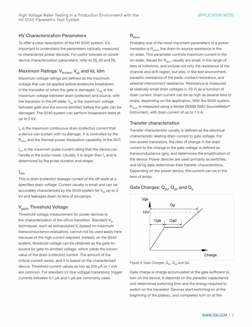
Gate Charges: Qgs, Qgd and Qg
Figure 3: Gate Charges, Qgs, Qgd and Qd.
Gate charge is charge accumulated at the gate sufficient to
turn on the device. It depends on the parasitic capacitance
and determines switching time and the energy required to
switch on the transistor. Devices start switching on at the
beginning of the plateau, and completely turn on at the

4 | WWW.TEK.COM
High Voltage Wafer Testing in a Production Environment with the HV S540 Parametric Test System
APPLICATION NOTE
right side of the plateau. To perform this measurement,
the instrumentation setup should be able to sustain high
current (Idon).
Device Capacitances: Cgd, Cgs, Cds and Ciss, Coss, Crss
Figure 4: Transistor capacitances: Cgd, Cgs and Cds.
Figure 5: Ciss, Coss and Crss.
Switching speed of the power devices is controlled by
the device capacitances. This includes capacitances
between gate and drain (Cgd), gate and source (Cgs),
and drain and source (Cds). The combination of these
capacitances (Ciss, Coss, Crss) characterizes input and output
transient performance. Ciss is equal to Cgs plus Cgd. It is the
capacitance that has to be charged for the transistor to be
switched on, and is the one that controls the speed of the
turn-on switching. Coss = Cds + Cdg is an output capacitance.
It affects circuit resonance and dynamic behavior. Crss (Cgd)
is the reverse transfer capacitance, sometimes called Miller
capacitance. This capacitance controls turn-off timing.
Figure 6: Ciss, Coss and Crss as a function of Vds, as measured by the S540 system.
Ciss, Coss and Crss are measured in the off-state, when Vgs = 0,
for different drain (Vds) biases (Figure 6).
Characterization and Production PCM Systems Requirements
The S540 system was designed for two scenarios: the first
is its use in process integration labs; the second is process
control monitoring (PCM) with automated testing. Each
scenario has slightly different requirements. In process
integration, all parameters usually need to be characterized,
and complexity in the setup and testing is acceptable. The
amount of data taken, throughput, and simplicity usually
are not significant factors. The flexibility of the test setup is
the primary factor. In PCM, only a subset of parameters is
collected. Throughput, simplicity and automation are the
primary factors.

WWW.TEK.COM | 5
High Voltage Wafer Testing in a Production Environment with the HV S540 Parametric Test System
APPLICATION NOTE
HV S540 Tests
Breakdown Test
HV breakdown tests usually are used to outline the usage
boundary of the device and to evaluate the stability of the
power devices in various scenarios. Breakdown happens in
various media, but most of the interest is in the breakdown of
material junctions, such as at the junction of the drain to gate
or substrate. Breakdown voltages depend on the materials
and the structure design. The S540 system is designed to
evaluate breakdown voltages of up to 3 kV.
Pad Pitch Distance Limitation
For packaged devices, isolation between HV voltage
terminals is relatively easy and usually is achieved through
the use of greater separation and insulating materials.
The situation is more complicated when the device is still on
the wafer as in PCM (Process Control Monitoring) testing.
Minimizing the amount of wafer real estate needed for test
structures is in conflict with the continuous drive for higher
breakdown voltages. Usually, the minimum pad pitch (the
distance between two adjacent pads) should be sufficient to
prevent arcing in the air. Maximum sustainable electrical field
in the dry air can be estimated be close to 40 kV/cm, or 4 V/
µm. To sustain 1.8 kV, for example, pad pitch size has to be
equal to or greater than 425 µm.
Electrical Field with Needles, Spherical, Cylindrical Field Concentration, Polymer Protection of the Needles
The maximum electrical field between flat metal pads can
be estimated to be close to V/d. The electrical field around
the metal needle is defined by the cylindrical geometry of the
needle. The electrical field will be at its maximum close to the
needle, and can be estimated to be close to V/R, where R is
the radius of the needle. Given that the radius of the needle
(25 µm, for example) is much smaller than the HV pad pitch
distance (300=600 µm) typically used, there is amplification
of the electrical field at the needles, by the ratio of d/R (see
Figure 7). For this particular case, the maximum electrical
field will be 12 to 24 times larger than the field estimated by
dividing the voltage by the pad distance. This illustrates the
potential challenges in the breakdown tests on the wafer,
when sufficient pad pitch size can still lead to air ionization
and air breakdown. Polymer or any other isolating coating on
the metal surface of the needles can suppress this effect, and
this technique is used by some probe cards makers (Celadon
Systems, for example).
d
V ( bias voltage )
E = V/d
RE = V/R
Figure 7: Pin to pad connection geometry
Wafer Surface Damage
Another complication of HV on-wafer testing is caused by the
presence of moisture on the surface of the wafer. Breakdown
test is supposed to test maximum voltage in the bulk of the
semiconductor material; however, surface breakdown often
prevents reaching these voltage levels.
Surface moisture significantly decreases the electrical
strength of the air, and moisture has to be suppressed by
the environmental control. The most common technique is
the use of jets of nitrogen or CDA (Clean Dry Air) into the
test area. This allows for somewhat increased electrical
strength of the air; however, all dry gases have comparable
electrical strength and at high enough voltages at given
device geometries, breakdown is unavoidable and happens
before breakdown in the bulk of the semiconductor
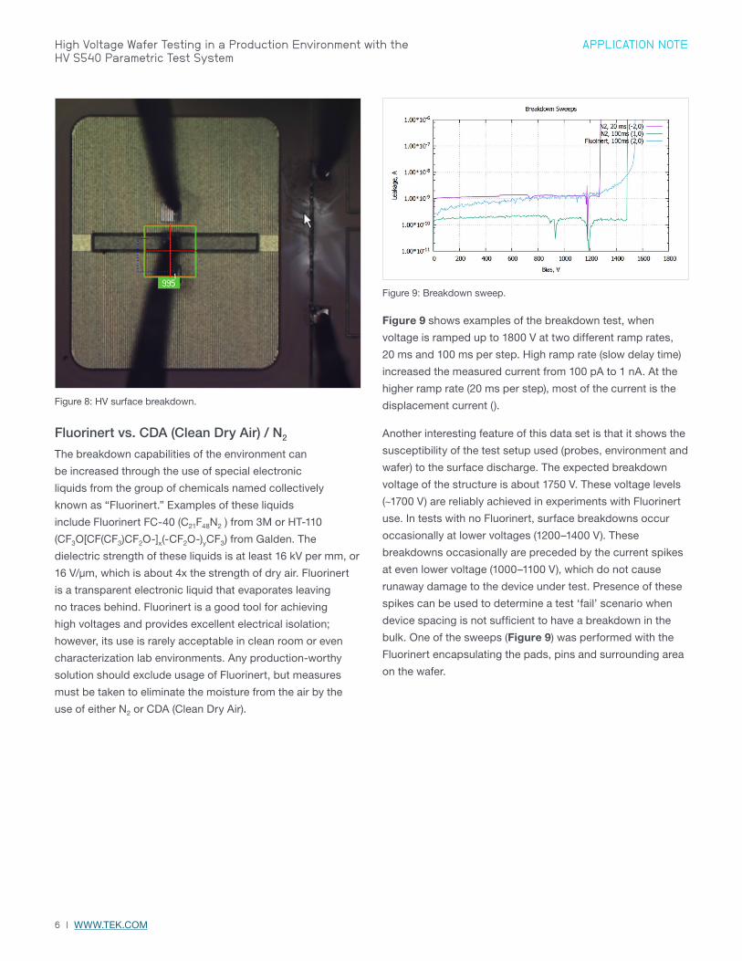
material (Figure 8). Pins to the left are for source and gate
connections; pads to the right are drain/bulk connections.
The distance between source and gate pads is about 600 µm.
Visual inspection of the damage indicates air breakdown
between source/gate needles to the drain connection on
the right.
6 | WWW.TEK.COM
High Voltage Wafer Testing in a Production Environment with the HV S540 Parametric Test System
APPLICATION NOTE
Figure 8: HV surface breakdown.
Fluorinert vs. CDA (Clean Dry Air) / N2
The breakdown capabilities of the environment can
be increased through the use of special electronic
liquids from the group of chemicals named collectively
known as “Fluorinert.” Examples of these liquids
include Fluorinert FC-40 (C21F48N2 ) from 3M or HT-110
(CF3O[CF(CF3)CF2O-]x(-CF2O-)yCF3) from Galden. The
dielectric strength of these liquids is at least 16 kV per mm, or
16 V/µm, which is about 4x the strength of dry air. Fluorinert
is a transparent electronic liquid that evaporates leaving
no traces behind. Fluorinert is a good tool for achieving
high voltages and provides excellent electrical isolation;
however, its use is rarely acceptable in clean room or even
characterization lab environments. Any production-worthy
solution should exclude usage of Fluorinert, but measures
must be taken to eliminate the moisture from the air by the
use of either N2 or CDA (Clean Dry Air).
Figure 9: Breakdown sweep.
Figure 9 shows examples of the breakdown test, when
voltage is ramped up to 1800 V at two different ramp rates,
20 ms and 100 ms per step. High ramp rate (slow delay time)
increased the measured current from 100 pA to 1 nA. At the
higher ramp rate (20 ms per step), most of the current is the
displacement current ().
Another interesting feature of this data set is that it shows the
susceptibility of the test setup used (probes, environment and
wafer) to the surface discharge. The expected breakdown
voltage of the structure is about 1750 V. These voltage levels
(~1700 V) are reliably achieved in experiments with Fluorinert
use. In tests with no Fluorinert, surface breakdowns occur
occasionally at lower voltages (1200–1400 V). These
breakdowns occasionally are preceded by the current spikes
at even lower voltage (1000–1100 V), which do not cause
runaway damage to the device under test. Presence of these
spikes can be used to determine a test ‘fail’ scenario when
device spacing is not sufficient to have a breakdown in the
bulk. One of the sweeps (Figure 9) was performed with the
Fluorinert encapsulating the pads, pins and surrounding area
on the wafer.

WWW.TEK.COM | 7
High Voltage Wafer Testing in a Production Environment with the HV S540 Parametric Test System
APPLICATION NOTE
Figure 10: Test area on the wafer encapsulated in the protective Fluorinert liquid.
Breakdown Measurement with Pressurized Cavities
Fluorinert works well in that it suppresses all discharges in
the air and allows measuring the intrinsic breakdown of the
devices; however, it is not a production solution. There is
an alternative to the use of the electronic insulating liquids:
pressurized cavities above the probe needle area (Figure 11).
An encapsulating cover on top of the probe card adaptor
creates a pressurized cavity filled with N2 or CDA, and forces
a stream of the gas along the probe needles.
It turns out that the pressurized cavity approach works just
as well as the Fluorinert approach, producing the same
breakdown voltages and IV data (Figure 12). The pressurized
cavity yields the same MEAN and STDEV for the breakdown
voltage as the Fluorinert does.
The use of pressurized cavities to suppress discharges is
relatively common in the industry, and the usual explanation
is that this suppression is the result of excessive pressure,
which increases the breakdown voltage. However, it appears
that the actual mechanism is not the pressure of the N2 but
rather the strong flow of the N2/CDA. This flow flushes ions
from the test area, suppressing ionization and the surface
discharge.
d
V ( bias voltage )
E = V/d
RE = V/R
Figure 11: Pressurized cavity on top of probe card insert (Celadon Systems).

8 | WWW.TEK.COM
High Voltage Wafer Testing in a Production Environment with the HV S540 Parametric Test System
APPLICATION NOTE
Energy Dissipation and the Needle Tip
Another aspect of the breakdown test with high voltages
(>1000 V) relative to LV (<200 V) is higher energy dissipation,
which has an impact on the durability and stability of the
pins and pin contacts. First, let’s estimate the total electrical
energy, which is dissipated during the breakdown. It
is given by:
E = ½CV2
Equation 1: Energy of the capacitance)
Here, C is the cable capacitance and V is the maximum
breakdown voltage. For 3-m-long Kelvin triaxial cables,
capacitance can be estimated to be close to 1 nF. With
breakdown voltage of 1700 V, the total energy stored in
the cable parasitic capacitance is about 1.4 mJ, which is
400 times larger than the energy dissipated during 85 V
breakdown. This is an energy difference of several orders of
magnitude and presents a very different usage scenario for
the probe tips. During breakdown, this energy will dissipate
in different parts of the test setup, for example, at the tested
drain/substrate junction or at the pin-to-pad contact. Any
bad contact, small prober overdrive, or the gap between
probe tip and the pad would lead to the concentration of the
energy dissipation to the probe tip, which may lead to pin
degradation or even melting. Assuming tungsten needles are
used, and with the specific heat of tungsten (0.134 J/gm K),
density of tungsten of 19.2 gm/cm3, and volume of the
impacted tip defined by the radius of 50 µm (or 5e-3 cm), a
simple estimate yields 10,000 K. For 85 V breakdown, for
example, heating would be limited only to 25 K, or 400 times
smaller. Of course, this calculation overestimates the heating
of the needle because it assumes that all energy released
would go to the tip; nevertheless, this estimate does illustrate
the potential issue, and the fact that, at high voltages, pins
can be easily melted, oxidized, or degraded.
The design of the Prober Card Adapter (PCA) with built-
in elements may help to limit the breakdown current and
damage to the needle tips.
High Voltage C-VIn power device characterization, 3-terminal capacitance
measurements (Ciss, Coss and Crss) are some of the most
requested and challenging measurements. These values
allow estimating the switch characteristics of the transistors
in terms of speed, energy, and charge required for switching.
The measurements are usually performed on the bench
setups in the labs, with interconnects that minimalize
parasitic capacitance. For the S540, we developed an
automated procedure that takes advantage of the HV matrix
and allows performing these measurements in the automated
environment.
Bias Tee 2-Terminal AC Model
To bias transistors to high voltage and measure capacitance,
any HV C-V technique has to use bias tees, which mix high
voltage DC bias voltage with an AC sense signal. Bias tee
usage leads to the degradation of the AC pathway and to
increased measurement errors. Before considering 3-terminal
capacitance measurements, let’s consider a 2-terminal setup
(Figure 13).
Figure 12: I-V data collected with Fluorinert and pressurized cavity.
WWW.TEK.COM | 9
High Voltage Wafer Testing in a Production Environment with the HV S540 Parametric Test System
APPLICATION NOTE
CMTRAC Impedance Meter
Bias-Tee
Cbt L
Bias-Tee
CL
CMTRAC Impedance Meter
Cp
Gp
DUT:Bias-Tee
Cbt L
Bias-Tee
L CbtCcable Ccable
CopenOPEN:
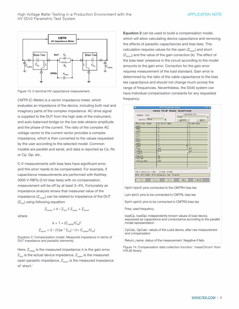
Figure 13: 2-terminal HV capacitance measurement.
CMTR (C-Meter) is a vector impedance meter, which
evaluates an impedance of the device, including both real and
imaginary parts of the complex impedance. AC drive signal
is supplied to the DUT from the high side of the instrument,
and auto-balanced bridge on the low side obtains amplitude
and the phase of the current. The ratio of the complex AC
voltage vector to the current vector provides a complex
impedance, which is then converted to the values requested
by the user according to the selected model. Common
models are parallel and serial, and data is reported as Cs, Rs
or Cp, Gp, etc.
C-V measurements with bias tees have significant error,
and this error needs to be compensated. For example, if
capacitance measurements are performed with Keithley
3000 V-RBTs (3 kV bias tees) with no compensation,
measurement will be off by at least 3–4%. Fortunately an
impedance analysis shows that measured value of the
impedance (Zmeas) can be related to impedance of the DUT
(Zdut) using following equation:
Zmeas = k * Zdut || Zopen + Zshort
where
k = 1 + (Ccable/Cbt)2
Zshort = 2 * (1/jw * Cbt) * (1+ Ccable/Cbt)
Equation 2: Compensation model. Measured impedance in terms of DUT impedance and parasitic elements)
Here, Zmeas is the measured impedance; k is the gain error,
Zdut is the actual device impedance, Zopen is the measured
open parasitic impedance, Zshort is the measured impedance
of ‘short.’
Equation 2 can be used to build a compensation model,
which will allow calculating device capacitance and removing
the effects of parasitic capacitances and bias tees. This
calculation requires values for the open (Zopen) and short
(Zshort) and the value of the gain correction (k). The effect of
the bias tees’ presence in the circuit according to the model
amounts to the gain error. Correction for the gain error
requires measurement of the load standard. Gain error is
determined by the ratio of the cable capacitance to the bias
tee capacitance and should not change much across the
range of frequencies. Nevertheless, the S540 system can
have individual compensation constants for any requested
frequency.
Hpin1-hpin3: pins connected to the CMTRH bias tee
Lpin-lpin3: pins to be connected to CMTRL bias tee
Epin1-epin3: pins to be connected to CMTRG bias tee
Freq: used frequency
loadCp, loadGp: independently known values of load device, expressed as capacitance and conductance according to the parallel model representation
CpCalc, GpCalc: values of the Load device, after raw measurement and compensation
Return_name: status of the measurement. Negative if fails.
Figure 14: Compensation data collection function: ‘measCVcom’ from HVLIB library.

10 | WWW.TEK.COM
High Voltage Wafer Testing in a Production Environment with the HV S540 Parametric Test System
APPLICATION NOTE
Figure 15: Open/Short/Load Correction factors in kth.ini
In the S540 system, we include system-level compensation,
which has two components. The first one is a characterization
procedure, shown in Figure 14, which measures known
Open/Short/Load standards in the factory and stores
constants to the system file, $KIHOME/kth.ini (Figure 15).
If the user employs a customized PCA adaptor or wants
to add an additional frequency, running a characterization
routine (measCVcomp from the HVLIB library), and manually
copying constants to the kth.ini file is recommended. This
characterization routine (measCVcomp routine from HVLIB)
prompts the user to connect to Open/Short and Load device.
Load device values have to be known and set in the input
arguments (see Figure 14 for values loadCp and loadGp. The
routine calculates a set of values for Short/Open/Load, which
then have to be copied manually to the kth.ini file.
A function “intgCG(inst, freq, Cp, Gp)” from HVLIB performs
raw measurements, and runs on-line data compensation
using data from kth.ini.
In addition to this system-level compensation, it’s possible to
do a user-level compensation for each individual pin-pair at
a run-time on the wafer during automated testing. Available
compensation methods are Open, Short, Load, OpenLoad,
ShortOpen and ShortOpenLoad. Short and Open devices
usually are easily available on the wafer. Open measurement
can be performed when the chuck is down. Short is available
on any metal surface/connected pads on the wafer. Selection
of the known Load device on the wafer can be a challenge
because it requires C-V characterization of the capacitor on
the wafer with no bias tee. Fortunately, load compensation
can be done using resistive load, which can be easily
characterized with DC (SMU) instruments. Resistive devices
are relatively easy to find and characterize on the wafer. For
example, polysilicon lines can be used for such standards
and characterized for DC resistance with standard DC
technology (SMUs).
Load
Device Cp Error
CAPACITANCE 1.03E-10
S540 1.07E-10 3.40%
Open 9.97E-11 –3.30%
Short 1.07E-10 3.80%
OpenShort 1.00E-10 –2.90%
OpenLoad 1nF 1 nF 1.06E-10 2.90%
ShortOpenLoad 1nF 1 nF 1.03E-10 0.20%
Load 11 kΩ 11 kΩ 1.09E-10 5.70%
OpenLoad 11 kΩ 11 kΩ 1.03E-10 0.20%
ShortOpenLoad 11 kΩ 11 kΩ 1.03E-10 0.00% Table 1: Correction effectiveness for different compensation models (Load, OpenLoad, and ShortOpenLoad)
Table 1 shows the effectiveness of compensation models.
The 103 pF capacitor was measured in different scenarios.
This included measurements performed with the S540
system and no correction, with Open correction only, Short,
OpenShort, OpenShortLoad corrections, etc. With no
compensation, the S540 system measures 106.6 pF (3.4%
error). Just ‘Open’, ‘Short’ or ‘OpenShort’ compensation
does not decrease the error. Two load devices were used in
the table, 1 nF and resistive load 11 kΩ. For all these loads,
‘ShortOpenLoad’ compensation works well, with total error
reduced to less than 0.2%.
A short description of the test code, which enables run-time
compensation per any pin, together with an example test
routine (CVtest), is provided in the Appendix 1. The appendix
provides details for the HV application test library, HVLIB.
3-Terminal Capacitance Measurements
As was mentioned previously, switching properties of the
power transistors can be derived from Ciss, Coss and Crss
(see Figure 4 and Figure 5). These measurements usually
are performed in the off-state, with gate voltage commonly
at 0 V DC and at high drain voltage. The need to apply high
WWW.TEK.COM | 11
High Voltage Wafer Testing in a Production Environment with the HV S540 Parametric Test System
APPLICATION NOTE
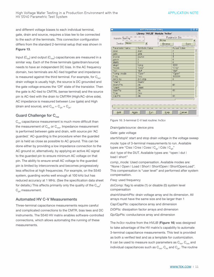
and different voltage biases to each individual terminal,
gate, drain and source, requires a bias tee to be connected
to the each of the terminals. This connection configuration
differs from the standard 2-terminal setup that was shown in
Figure 13.
Input (Ciss) and output (Coss) capacitances are measured in a
similar way. Each of the three terminals (gate/drain/source)
needs to have an independent DC bias. In the AC frequency
domain, two terminals are AC-tied together and impedance
is measured against the third terminal. For example, for Ciss,
drain voltage is usually high, the source is DC grounded and
the gate voltage ensures the ‘Off’ state of the transistor. Then
the gate is AC-tied to CMTRL (sense terminal) and the source
pin is AC-tied with the drain to CMTRH (High/AC-drive side).
AC impedance is measured between Low (gate) and High
(drain and source), and Ciss = Cgd + Cgs.
Guard Challenge for Crss
Crss capacitance measurement is much more difficult than
the measurement of Ciss or Coss. Impedance measurement
is performed between gate and drain, with source pin ‘AC
guarded.’ AC-guarding is the procedure when the guarded
pin is held as close as possible to AC ground. This can be
done either by providing a low impedance connection to the
AC ground or, alternatively, by applying an active AC signal
to the guarded pin to ensure minimum AC voltage on that
pin. The ability to ensure small AC voltage to the guarded
pin is limited by interconnects and becomes progressively
less effective at high frequencies. For example, on the S540
system, guarding works well enough at 100 kHz but has
reduced accuracy at 1 MHz. (See the specification data sheet
for details.) This affects primarily only the quality of the Crss/
Cgd measurement.
Automated HV C-V Measurements
Three-terminal capacitance measurements require careful
and complicated connections to the CMTR, bias tees and DC
instruments. The S540 HV matrix enables software-controlled
connections, which allows automating the running of these
measurements.
Figure 16: 3-terminal C-V test routine: hv3cv
Drain/gate/source: device pins
Gate: gate voltage
startV/stopV: start and stop drain voltage in the voltage sweep
mode: type of 3-terminal measurements to run. Available types are “Ciss | Crss | Coss | Cgs | Cds | Cgd”
dut: type of the DUT. Available types are: “open | dut | load | short”
comp_mode: Used compensation. Available modes are: “None | Open | Load | Short | ShortOpen | ShortOpenLoad”. This compensation is “user level” and performed after system compensation.
Freq: used frequency
doComp: flag to enable (1) or disable (0) system level compensation
drainV/drainVPts: drain voltage array and its dimension. All arrays must have the same size and be larger than 1
Cap/CapPts: capacitance array and dimension
D/DPts: dissipation factor arrays and dimension
Gp/GpPts: conductance array and dimension
The hv3cv routine from the HVLIB (Figure 16) was designed
to take advantage of the HV matrix’s capability to automate
3-terminal capacitance measurements. This test is provided
as both a verified test and as a template for customization.
It can be used to measure such parameters as Ciss, Coss and
individual capacitances such as Crss, Cds and Cgs. The routine

12 | WWW.TEK.COM
High Voltage Wafer Testing in a Production Environment with the HV S540 Parametric Test System
APPLICATION NOTE
will use system-level compensation when the “doComp”
flag is enabled. In addition to that, the routine will perform
additional device-level compensations, including most
of the known compensation models. To run, for example,
“ShortOpenLoad” device-level compensation, data needs to
be collected from the Open, Short and Load devices.
Figure 17: Storing of Open data for capacitance compensation.
Figure 17 shows an example of “open” only device-level
compensation. Here, data obtained elsewhere is stored to
the system using storeCVdata under a unique label, ‘D8_G7_
S6_Mode:Crss’. The following test, hv3cv, uses this data and
completes open correction.
Figure 18: Test parts for 3-terminal C-V evaluation.
The S540 system’s 3-terminal HV C-V procedure was
evaluated using discrete parts, similar to the ones shown in
Figure 18. Test capacitors were pre-evaluated and were built
into several transistor configurations, as shown in Figure 4.
Table 2: 3-terminal HV C-V evaluation data
Table 2 shows data for three capacitor configurations
(Cgs, Cgd, and Cds). Three configurations were selected
for various ratios of Cgs:Cds:Cgd capacitances. Ratios
tested here: 1:0.1:0.01, 1:1:0.1 and 1:0.02:0.02. The larger
the ratio, the less accuracy can be expected from smaller
capacitance measurements. Expected values of Ciss, Coss
and Crss are calculated and compared against measured
values. The measurement procedure included system-
level OpenShortLoad compensation, and DUT-level Open
compensation. The last column shows the deviation of the
measured values from those expected.
Figure 6 shows the HV C-V data for Crss, Ciss and Coss
measured at various drain biases, ranging from 0 V to
1000 V. Data were collected using the S540 system, with all
interconnect changes and AC guarding setup performed by
the HV matrix and under automated software control.
Automated test sequence
LV, HV and C-V measurements to any pin
The S540 system was designed to run standard parametric
measurements (LV characterization, C-V, etc.) in a single pass
together with HV measurements (HV breakdown test, HV C-V,
3-terminal HV C-V).

WWW.TEK.COM | 13
High Voltage Wafer Testing in a Production Environment with the HV S540 Parametric Test System
APPLICATION NOTE
Figure 19: Sample of S540 test sequence.
Figure 19 shows an example of a test sequence performed
on one of the subsites (scribe test module). This sequence
includes standard LV transistor characterization (threshold
voltage: hvlib_vtlin, drain current: hvlib_id) and HV tests
(breakdown tests: hvlib_bkdn, hvlib_bvswep; and leakage
test: hvlib_leak). The names of these tests and library
were taken from one of the demonstration tests. Due to
the destructive nature of the HV tests, these tests usually
are done at the end of the sequence. From the user’s
perspective, there is no differentiation between HV, LV and
C-V tests. The system handles all the switching, interconnect
issues, protection of the user and instrumentation, and
interfacing to the wafer with the probe card adaptor.
Figure 20: Throughput analysis.
The S540 system is designed as a production system.
In addition to the requirement to run all tests (LV, HV and
HV C-V) in a single pass, it’s also desirable to run the
tests as fast as possible to satisfy production throughput
requirements. HV tests often take longer to run due to the
capacitive nature of the DUT and higher required voltage
values. Nevertheless, because throughput is always
important, the S540 system includes a tool for throughput
analysis and optimization. Figure 20 shows a throughput
analysis performed on production log data using the
ptlog utility.
Low Voltage/Sensitive Measurement through HV Matrix and HV Interconnects
Figure 21: Id-Vg data. Vds = 0.1V.
The addition of the 3 kV HV capability to this production
system does not degrade the accuracy of its sensitive LV
parametric measurements. The S540 system includes
both HV instrumentation (Model 2657A High Power System
SourceMeter® SMU Instrument) and LV sensitive SMUs
(Model 2636B Dual-channel System SourceMeter SMU
Instrument with 0.1fA sensitivity). Figure 21 shows Id/Vg
data taken at small drain voltage (0.1 V) and demonstrates
low current capability. Idoff current for this device is about
100 pA. With the chuck down, the current would drop to the
noise floor of the system, which is in the range of less than
10 picoamps.

14 | WWW.TEK.COM
High Voltage Wafer Testing in a Production Environment with the HV S540 Parametric Test System
APPLICATION NOTE
S540 System Configurations
HV Matrix
12 Pin Max
HV SMUs(3000V)
LV SMUs(200V)
LV CAP(40V) DMM Scope,
PGU
HV CAP(3000V)
HV Chuck
12 PinPCA
Figure 22: 3 kV HV system.
The S540 system comes in two versions: “3 kV only system”
and “Hybrid” system. The 3 kV system (Figure 22) contains a
12×12 HV matrix, with 12 input rows and 12 output columns.
Each output is 3 kV-enabled, and can be connected either to
an HV Probe Card Adapter or an HV chuck connection. It can
also be used to provide HV bias to up to three HV bias tees.
3 kV HV System Only, HV matrix with 12 pins
The S540 system can be configured with up to three bias
tees for HV C-V measurements. As discussed previously,
C-measurements made with bias tees have to be corrected to
account for their presence. This can be done on the system
level and per specific device on the user level. In addition to
the CMTR (installed in the 4200-SCS Parametric Analyzer),
the S540 system contains two HV SMUs (Model 2657As),
and up to six Model 2636B SMUs. Protection modules
allow using low voltage SMUs (like the Model 2636B with
<200 V) together with HV for sensitive measurements. A low
patch panel provides a ground reference point for the all
instruments. HV, LV, and C-V signals can be provided to any
of the probe pins.
Hybrid 3 kV HV and Sensitive System
HV Matrix6 Pin
Pass-Thru
36 Pin Max
HV SMUs(3000V)
LV SMUs(200V)
LV CAP(40V) DMM Scope,
PGU
HV CAP(3000V)
HV Chuck
48 PinPCA
LC Matrix
12 Pin Max
Figure 23: Hybrid system: 3 kV + LV.
The 3 kV HV matrix has 12 HV pins. For example, for a
system with three bias tees, with an HV chuck and a total
12 HV matrix columns, there are eight HV pins available for
the Probe Card Adapter (PCA). For some customers in a
production environment, it is desirable to run a larger set of
output pins. The hybrid system, Figure 23, was designed for
this requirement. In addition to a few (8–12) HV pins, an S540
hybrid system allows using up to 36 standard LV pins for
automated testing.
WWW.TEK.COM | 15
High Voltage Wafer Testing in a Production Environment with the HV S540 Parametric Test System
APPLICATION NOTE
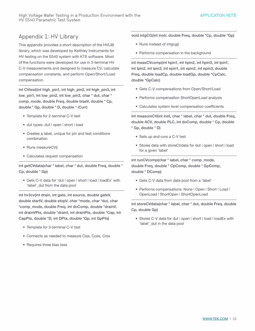
Appendix 1: HV LibraryThis appendix provides a short description of the HVLIB
library, which was developed by Keithley Instruments for
HV testing on the S540 system with KTE software. Most
of the functions were developed for use in 3-terminal HV
C-V measurements and designed to measure CV, calculate
compensation constants, and perform Open/Short/Load
compensation.
int CVtest(int high_pin1, int high_pin2, int high_pin3, int
low_pin1, int low_pin2, int low_pin3, char * dut, char *
comp_mode, double Freq, double biasV, double * Cp,
double * Gp, double * D, double * iCurr)
• Template for 2-terminal C-V test
• dut types: dut | open | short | load
• Creates a label, unique for pin and test conditions combination
• Runs measureCV()
• Calculates request compensation
int getCVdata(char * label, char * dut, double Freq, double *
Cp, double * Gp)
• Gets C-V data for ‘dut | open | short | load | loadEx’ with ‘label’_dut from the data pool
int hv3cv(int drain, int gate, int source, double gateV,
double startV, double stopV, char *mode, char *dut, char
*comp_mode, double Freq, int doComp, double *drainV,
int drainVPts, double *drainI, int drainPts, double *Cap, int
CapPts, double *D, int DPts, double *Gp, int GpPts)
• Template for 3-terminal C-V test
• Connects as needed to measure Ciss, Coss, Crss
• Requires three bias tees
void intgCG(int instr, double Freq, double *Cp, double *Gp)
• Runs instead of intgcg()
• Performs compensation in the background
int measCVcomp(int hpin1, int hpin2, int hpin3, int lpin1,
int lpin2, int lpin3, int epin1, int epin2, int epin3, double
Freq, double loadCp, double loadGp, double *CpCalc,
double *GpCalc)
• Gets C-V compensations from Open/Short/Load
• Performs compensation ShortOpenLoad analysis
• Calculates system level compensation coefficients
int measureCV(int inst, char * label, char * dut, double Freq,
double ACV, double PLC, int doComp, double * Cp, double
* Gp, double * D)
• Sets up and runs a C-V test
• Stores data with storeCVdata for dut | open | short | load for a given ‘label’
int runCVcomp(char * label, char * comp_mode,
double Freq, double * CpComp, double * GpComp,
double * DComp)
• Gets C-V data from data pool from a ‘label’
• Performs compensations: None | Open | Short | Load | OpenLoad | ShortOpen | ShortOpenLoad
int storeCVdata(char * label, char * dut, double Freq, double
Cp, double Gp)
• Stores C-V data for dut | open | short | load | loadEx with ‘label’_dut in the data pool

16 | WWW.TEK.COM
High Voltage Wafer Testing in a Production Environment with the HV S540 Parametric Test System
APPLICATION NOTE
References[1] D. K. Madjour, Silicon Carbide market update: From
discrete devices to modules. PCIM Europe 2014.
Nuremberg. [Online]. Available: http://apps.richardsonrfpd.com/Mktg/Tech-Hub/pdfs/YOLEPCIM_2014_SiC_Market_ARROW_KMA_Yole-final.pdf. Accessed on:
September 30, 2016.
[2] Customized probe card for on-wafer testing of AlGaN/
GaN power transistors. R. Venegas. COMPASS, 2015.
[Online]. Available: http://www.celadonsystems.com/wp-content/uploads/2016/06/Final_COMPASS2015_imecKA090715.pdf. Accessed on: September 30, 2016.
[3] Power MOSFET Tutorial. Jonathan Dodge, P.E.
Advanced Power Technology. 2006. [Online].
Available: http://www.microsemi.com/document-portal/doc_view/14692-mosfet-tutorial. Accessed on:
September 30, 2016.
[4] Power MOSFET Basics, Alpha and Omega
Semiconductor, 2008. [Online]. Available: http://www.aosmd.com/res/application_notes/mosfets/Power_MOSFET_Basics.pdf. Accessed on: September 30, 2016.
[5] Understanding power MOSFET data sheet parameters.
NXP. 2014 [Online]. Available: http://www.nxp.com/documents/application_note/AN11158.pdf. Accessed on:
September 30, 2016.

High Voltage Wafer Testing in a Production Environment with the HV S540 Parametric Test System
APPLICATION NOTE
Contact Information: Australia* 1 800 709 465
Austria 00800 2255 4835
Balkans, Israel, South Africa and other ISE Countries +41 52 675 3777
Belgium* 00800 2255 4835
Brazil +55 (11) 3759 7627
Canada 1 800 833 9200
Central East Europe / Baltics +41 52 675 3777
Central Europe / Greece +41 52 675 3777
Denmark +45 80 88 1401
Finland +41 52 675 3777
France* 00800 2255 4835
Germany* 00800 2255 4835
Hong Kong 400 820 5835
India 000 800 650 1835
Indonesia 007 803 601 5249
Italy 00800 2255 4835
Japan 81 (3) 6714 3010
Luxembourg +41 52 675 3777
Malaysia 1 800 22 55835
Mexico, Central/South America and Caribbean 52 (55) 56 04 50 90
Middle East, Asia, and North Africa +41 52 675 3777
The Netherlands* 00800 2255 4835
New Zealand 0800 800 238
Norway 800 16098
People’s Republic of China 400 820 5835
Philippines 1 800 1601 0077
Poland +41 52 675 3777
Portugal 80 08 12370
Republic of Korea +82 2 6917 5000
Russia / CIS +7 (495) 6647564
Singapore 800 6011 473
South Africa +41 52 675 3777
Spain* 00800 2255 4835
Sweden* 00800 2255 4835
Switzerland* 00800 2255 4835
Taiwan 886 (2) 2656 6688
Thailand 1 800 011 931
United Kingdom / Ireland* 00800 2255 4835
USA 1 800 833 9200
Vietnam 12060128
* European toll-free number. If not accessible, call: +41 52 675 3777
Find more valuable resources at tek.comCopyright © Tektronix. All rights reserved. Tektronix products are covered by U.S. and foreign patents, issued and pending. Information in this publication supersedes that in all previously published material. Specification and price change privileges reserved. TEKTRONIX and TEK are registered trademarks of Tektronix, Inc. All other trade names referenced are the service marks, trademarks or registered trademarks of their respective companies.
102116.sbg 1KW-60936-0